Fabrication Technology for a Type of FR4 Semi-Flexible PCB

In the ever-evolving world of electronics, the demand for flexible and adaptable circuit board solutions continues to grow. One innovative approach that has gained traction is the development of semi-flexible PCBs using FR4 material. This article delves into the fabrication technology behind a type of FR4 semi-flexible PCB, exploring the processes, challenges, and advantages of this unique approach to circuit board design.

YouTube video

Understanding FR4 Material

FR4 (Flame Retardant 4) is a composite material widely used in the production of rigid printed circuit boards. It consists of a woven fiberglass cloth impregnated with an epoxy resin binder. The material is known for its excellent electrical insulation properties, mechanical strength, and flame resistance.

Key Properties of FR4

PropertyTypical Value
Dielectric Constant4.2-4.8
Dissipation Factor0.017-0.019
Glass Transition Temperature (Tg)130-180ยฐC
Coefficient of Thermal Expansion (CTE)50-70 ppm/ยฐC
Flexural Strength450-560 MPa
Water Absorption0.1-0.3%

While FR4 is traditionally used for rigid PCBs, innovative fabrication techniques have made it possible to create semi-flexible variants, combining the benefits of FR4 with limited flexibility in specific areas of the board.

Semi-Flexible PCB Concept

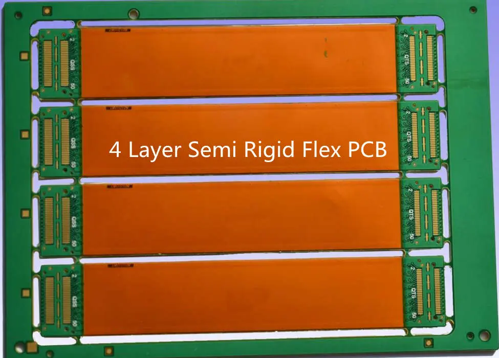
Semi-flexible PCBs, also known as rigid-flex PCBs, combine the characteristics of both rigid and flexible circuit boards. In the case of FR4 semi-flexible PCBs, the majority of the board maintains the rigidity of standard FR4, while specific areas are engineered to allow for controlled flexibility.

Key Features of FR4 Semi-Flexible PCBs

  1. Rigid FR4 sections for component mounting and structural integrity
  2. Flexible sections for interconnections or adaptable positioning
  3. Reduced overall thickness compared to traditional rigid PCBs
  4. Ability to bend or fold in predefined areas
  5. Improved resistance to vibration and mechanical stress

Design Considerations for FR4 Semi-Flexible PCBs

Designing FR4 semi-flexible PCBs requires careful consideration of several factors:

  1. Flex Zone Planning: Determine the areas that require flexibility and design the board layout accordingly.
  2. Layer Stack-up: Design an appropriate layer stack-up that accommodates both rigid and flexible sections.
  3. Copper Weight: Choose appropriate copper weights for both rigid and flexible areas.
  4. Bend Radius: Calculate and specify the minimum bend radius for flexible sections.
  5. Component Placement: Ensure components are placed away from flex zones to prevent stress on solder joints.
  6. Trace Routing: Design traces in flexible areas to withstand bending stress, using techniques like curved traces.

Material Selection and Preparation

The choice of materials for FR4 semi-flexible PCBs is crucial to achieving the desired balance between rigidity and flexibility.
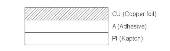
Material Components

  1. FR4 Core: Standard FR4 material for rigid sections
  2. Flexible Core: Thin FR4 or polyimide material for flexible areas
  3. Copper Foil: Rolled annealed copper for improved flex life
  4. Adhesives: Special adhesives to bond flexible and rigid sections
  5. Coverlay: Protective layer for flexible areas

Material Preparation Steps

  1. Cut FR4 cores to size
  2. Prepare flexible core materials
  3. Clean and treat copper foils
  4. Prepare adhesive sheets
  5. Cut coverlay materials to size

Fabrication Process Overview

The fabrication of FR4 semi-flexible PCBs involves a series of specialized processes:

  1. Material preparation
  2. Lamination
  3. Drilling and via formation
  4. Copper patterning and etching
  5. Flexible area creation
  6. Surface finish application
  7. Solder mask and legend application
  8. Electrical testing
  9. Mechanical processing
  10. Final inspection and quality control

Lamination Techniques

Lamination is a critical step in creating the foundation of the FR4 semi-flexible PCB.

Lamination Process Steps

  1. Layer Stack-up: Arrange FR4 cores, flexible materials, copper foils, and adhesive sheets according to the design.
  2. Press Preparation: Clean and prepare the lamination press plates.
  3. Material Loading: Carefully load the stack-up into the lamination press.
  4. Vacuum Application: Apply vacuum to remove air and prevent void formation.
  5. Heat and Pressure Cycle: Apply heat and pressure according to a predetermined profile.
  6. Cooling: Gradually cool the laminated stack under controlled conditions.

Typical Lamination Parameters

ParameterValue Range
Temperature175-200ยฐC
Pressure200-400 PSI
Time60-120 minutes
Vacuum28-30 inHg

Drilling and Via Formation

Drilling is performed to create holes for vias and component mounting.

Drilling Techniques

  1. Mechanical Drilling: Using high-speed CNC drilling machines for larger holes.
  2. Laser Drilling: Employing laser systems for small, high-precision holes, especially in flexible areas.

Via Formation Process

  1. Hole Cleaning: Remove debris and smooth hole walls.
  2. Desmear Process: Chemical treatment to remove resin smear.
  3. Electroless Copper Deposition: Deposit a thin layer of copper on hole walls.
  4. Copper Electroplating: Build up copper thickness in holes.

Copper Patterning and Etching

rigid-flex-pcb-design

Creating the circuit pattern involves a series of steps to accurately define the copper traces.

Copper Patterning Steps

  1. Photoresist Application: Apply dry film or liquid photoresist to the copper surface.
  2. Exposure: Use photolithography to transfer the circuit pattern to the photoresist.
  3. Development: Remove unexposed photoresist, revealing the desired copper pattern.
  4. Etching: Chemically remove exposed copper, leaving the protected circuit pattern.
  5. Resist Stripping: Remove remaining photoresist.

Etching Techniques

  1. Ammoniacal Etching: Using ammonia-based etchants for better undercut control.
  2. Cupric Chloride Etching: Offering faster etching rates but requiring careful process control.

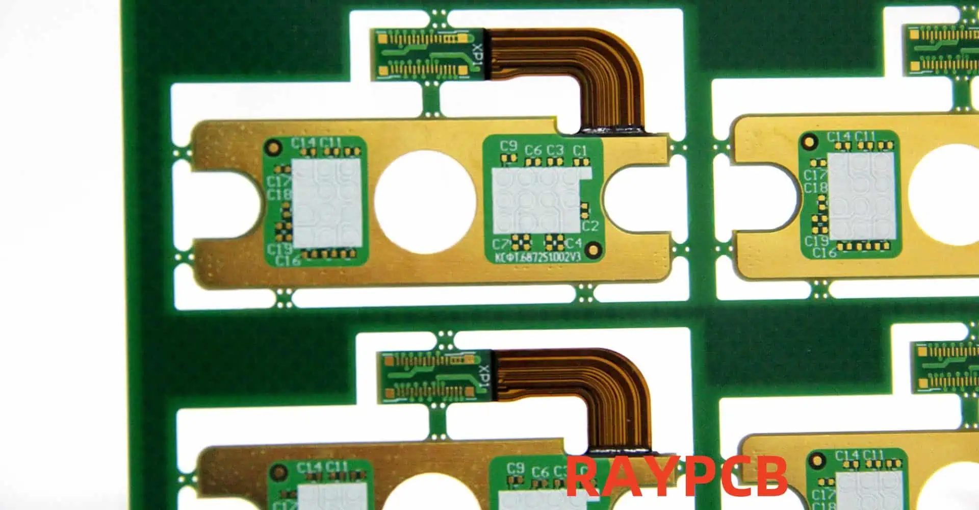
Flexible Area Creation

The key to FR4 semi-flexible PCBs lies in the creation of controlled flexible areas.

Flexible Area Formation Techniques

  1. Selective Core Removal: Mechanically or chemically remove FR4 core in designated flex areas.
  2. Thin Core Lamination: Use ultra-thin FR4 or polyimide cores in flexible sections during lamination.
  3. Laser Ablation: Precisely remove material using laser technology to create flex zones.

Considerations for Flexible Areas

  1. Thickness Control: Maintain consistent thickness in flexible sections.
  2. Adhesion: Ensure proper adhesion between flexible and rigid sections.
  3. Stress Relief: Design proper transitions between rigid and flexible areas to minimize stress.

Surface Finish Application

Applying appropriate surface finishes protects exposed copper and enhances solderability.

Common Surface Finishes for FR4 Semi-Flexible PCBs

Finish TypeCharacteristicsTypical Thickness
ENIG (Electroless Nickel Immersion Gold)Good solderability, flat surfaceNi: 3-6 ยตm, Au: 0.05-0.1 ยตm
HASL (Hot Air Solder Leveling)Cost-effective, good solderability1-40 ยตm
Immersion TinGood solderability, flat surface0.6-1.2 ยตm
OSP (Organic Solderability Preservative)Thin coating, environmentally friendly0.2-0.5 ยตm

Solder Mask and Legend

Applying solder mask and legend (silkscreen) is crucial for protection and identification.

Solder Mask Application Process

  1. Surface Preparation: Clean and micro-etch the copper surface.
  2. Solder Mask Application: Apply liquid photoimageable solder mask.
  3. Exposure and Development: Define solder mask openings using photolithography.
  4. Curing: Thermally cure the solder mask for durability.
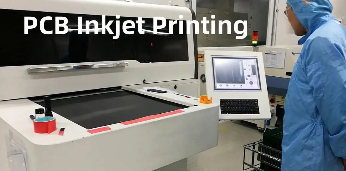
Legend Application

  1. Screen Printing: Apply legend ink using a screen printing process.
  2. Inkjet Printing: Use digital inkjet technology for high-resolution legends.
  3. Curing: Cure the legend ink according to manufacturer specifications.

Electrical Testing

Thorough electrical testing ensures the functionality and reliability of the FR4 semi-flexible PCB.

Testing Methods

  1. Continuity Testing: Verify electrical connections between points.
  2. Isolation Testing: Check for shorts between isolated circuits.
  3. Impedance Testing: Measure controlled impedance traces.
  4. Functional Testing: Perform specific functional tests as required by the design.

Mechanical Processing

Final mechanical processing prepares the board for use.

Processing Steps

  1. Routing: Cut the board to its final shape using CNC routing equipment.
  2. Scoring: Create V-grooves for board separation in panelized designs.
  3. Drilling: Perform any final drilling operations.
  4. Bending: Pre-form boards with required bends, if applicable.

Quality Control and Inspection

Rigorous quality control and inspection processes ensure the reliability of FR4 semi-flexible PCBs.

Inspection Techniques

  1. Visual Inspection: Check for physical defects and cosmetic issues.
  2. X-ray Inspection: Examine internal structures and hidden features.
  3. AOI (Automated Optical Inspection): Use machine vision systems for high-speed, accurate inspection.
  4. Cross-sectioning: Analyze internal structure and layer alignment.

Key Quality Parameters

ParameterTypical Tolerance
Line Width/Spacingยฑ10%
Hole Sizeยฑ0.075 mm
Layer-to-Layer Registrationยฑ0.075 mm
Bend RadiusAs per design specification
Solder Mask Thickness10-25 ยตm

Advantages and Limitations

FR4 semi-flexible PCBs offer unique advantages but also have certain limitations.

Advantages

  1. Combines benefits of rigid and flexible PCBs
  2. Reduced overall thickness compared to traditional rigid-flex designs
  3. Cost-effective for certain applications
  4. Familiar FR4 material properties in rigid sections
  5. Improved reliability in high-vibration environments

Limitations

  1. Limited flexibility compared to fully flexible PCBs
  2. Higher minimum bend radius than polyimide-based flexible circuits
  3. Potential for delamination in flex areas if not properly designed
  4. Limited to simpler flex designs compared to advanced rigid-flex technologies

Applications of FR4 Semi-Flexible PCBs

FR4 semi-flexible PCBs find applications in various industries:

  1. Automotive: Dashboard electronics, door panel controls
  2. Consumer Electronics: Foldable devices, wearable technology
  3. Industrial Equipment: Control panels with movable sections
  4. Medical Devices: Compact diagnostic equipment
  5. Aerospace: Non-critical flexible interconnects in space-constrained areas

Future Trends in Semi-Flexible PCB Technology

The field of semi-flexible PCB technology continues to evolve:

  1. Advanced Materials: Development of new FR4-like materials with enhanced flexibility
  2. Miniaturization: Pushing the limits of line width/spacing in flexible areas
  3. Additive Manufacturing: Exploring 3D printing techniques for semi-flexible PCBs
  4. Integrated Components: Embedding flexible components directly into semi-flexible structures
  5. Enhanced Automation: Improving manufacturing processes for higher volume production

Frequently Asked Questions

1. What is the maximum number of layers possible in an FR4 semi-flexible PCB?

The number of layers in an FR4 semi-flexible PCB typically ranges from 2 to 8 layers. However, it’s possible to create designs with more layers, up to 12 or even 14, depending on the specific requirements and manufacturing capabilities. As the number of layers increases, managing the overall thickness and flexibility becomes more challenging, especially in the flexible areas.

2. How does the bend radius of an FR4 semi-flexible PCB compare to a traditional flexible PCB?

FR4 semi-flexible PCBs generally have a larger minimum bend radius compared to traditional flexible PCBs made with polyimide materials. While a polyimide-based flexible PCB might achieve bend radii as small as 3-6 times the overall thickness, FR4 semi-flexible PCBs typically require bend radii of 10-20 times the thickness in the flexible areas. The exact bend radius depends on factors such as the specific materials used, the number of layers, and the copper thickness in the flexible section.

3. Can FR4 semi-flexible PCBs withstand repeated flexing?

FR4 semi-flexible PCBs are designed to withstand a limited number of flex cycles, typically in the range of hundreds to a few thousand cycles, depending on the design and materials used. They are not intended for applications requiring continuous or high-frequency flexing. For designs requiring frequent or continuous flexing, traditional flexible PCB materials like polyimide are more suitable. FR4 semi-flexible PCBs are best suited for applications where occasional flexing or a fixed bend is needed.

4. What are the key challenges in manufacturing FR4 semi-flexible PCBs?

Manufacturing FR4 semi-flexible PCBs presents several challenges:

  1. Material Transition: Ensuring a smooth transition between rigid and flexible areas without delamination or stress concentration.
  2. Thickness Control: Maintaining consistent thickness in flexible areas, especially when selectively removing FR4 material.
  3. Registration: Achieving accurate layer-to-layer registration between rigid and flexible sections.
  4. Copper Integrity: Preventing copper cracking in flexible areas during the manufacturing process and in use.
  5. Solder Mask Application: Applying solder mask that can withstand bending in flexible areas without cracking or peeling.

Addressing these challenges requires precise process control and potentially specialized equipment or techniques.

How to Analyze and Prohibit Impedance of High-Speed PCB Power

In the realm of high-speed printed circuit board (PCB) design, power integrity is a critical factor that can make or break the performance of electronic devices. As clock speeds increase and components become more power-hungry, the need for effective impedance control in PCB power distribution networks (PDNs) becomes paramount. This comprehensive guide delves into the intricacies of analyzing and prohibiting impedance in high-speed PCB power systems, providing engineers and designers with the knowledge and tools necessary to create robust and efficient power delivery solutions.

YouTube video

Understanding Impedance in High-Speed PCB Power

Impedance in PCB power systems refers to the opposition that a circuit presents to the flow of electrical current when a voltage is applied. In high-speed designs, impedance becomes a complex quantity that varies with frequency and consists of both resistive and reactive components.

Components of Impedance

  1. Resistance (R): The real part of impedance, representing the opposition to DC current flow.
  2. Inductance (L): The imaginary part of impedance that opposes changes in current flow.
  3. Capacitance (C): The imaginary part of impedance that opposes changes in voltage.

The total impedance (Z) is given by the formula:

Z = R + j(ฯ‰L – 1/ฯ‰C)

Where:

  • ฯ‰ is the angular frequency (2ฯ€f)
  • j is the imaginary unit

Importance of Impedance Control

Controlling impedance in high-speed PCB power systems is crucial for several reasons:

  1. Voltage Stability: Minimize voltage fluctuations at IC power pins.
  2. Signal Integrity: Reduce noise and maintain clean signal transitions.
  3. EMI Reduction: Minimize electromagnetic interference and improve EMC compliance.
  4. Power Efficiency: Optimize power delivery and reduce losses.
  5. Thermal Management: Reduce hotspots and improve overall thermal performance.

Factors Affecting PCB Power Impedance

Several factors contribute to the impedance characteristics of a PCB power system:

  1. PCB Stack-up: Layer count, thickness, and material properties.
  2. Power Plane Design: Size, shape, and spacing of power and ground planes.
  3. Via Design: Size, placement, and density of power and ground vias.
  4. Decoupling Strategy: Selection and placement of decoupling capacitors.
  5. Trace Geometry: Width, length, and spacing of power traces.
  6. Component Placement: Proximity of ICs to power sources and decoupling components.
  7. Frequency: Operating frequencies of the circuits and their harmonics.

Analyzing PCB Power Impedance

Effective impedance analysis involves a combination of theoretical calculations, simulations, and measurements. The goal is to create a comprehensive model of the power distribution network that accurately predicts its behavior across a wide range of frequencies.

Steps in Impedance Analysis

  1. Define Requirements: Establish target impedance based on IC specifications and system requirements.
  2. Create PDN Model: Develop an equivalent circuit model of the power distribution network.
  3. Perform Simulations: Use specialized software to simulate PDN behavior.
  4. Analyze Results: Examine impedance profiles, voltage ripple, and current distribution.
  5. Optimize Design: Iteratively refine the design to meet target impedance goals.
  6. Validate: Perform measurements on prototype boards to verify simulation results.

Tools and Techniques for Impedance Analysis

Several tools and techniques are available for analyzing PCB power impedance:

Tool/TechniqueDescriptionAdvantagesLimitations
SPICE SimulationCircuit-level simulation of PDNDetailed component-level analysisCan be computationally intensive for large designs
2D/3D EM SimulationElectromagnetic field simulationAccurate modeling of complex geometriesRequires significant computational resources
VNA MeasurementsVector Network Analyzer for S-parameter measurementsProvides real-world dataRequires specialized equipment and careful setup
TDR MeasurementsTime Domain Reflectometry for impedance profilingCan identify specific locations of impedance discontinuitiesLimited frequency range compared to VNA
Impedance AnalyzerDedicated instrument for impedance measurementsHigh accurac

Impedance Calculation Methods

Several methods can be used to calculate PCB power impedance:

1. Transmission Line Theory

For simple geometries, transmission line theory can provide quick estimates of characteristic impedance:

Zโ‚€ = โˆš(L/C)

Where:

  • Zโ‚€ is the characteristic impedance
  • L is the inductance per unit length
  • C is the capacitance per unit length

2. Cavity Model

The cavity model is useful for analyzing parallel plate structures:

Z = j2ฯ€fL(1 – (f/fโ‚€)ยฒ)

Where:

  • f is the frequency of interest
  • fโ‚€ is the resonant frequency of the cavity
  • L is the inductance of the cavity

3. Numerical Methods

For complex geometries, numerical methods such as the Finite Element Method (FEM) or Method of Moments (MoM) are employed in electromagnetic simulation software.

Strategies to Prohibit Unwanted Impedance

Controlling and minimizing unwanted impedance in high-speed PCB power systems involves several strategies:

  1. Proper PCB Stack-up Design: Optimize layer arrangement and thicknesses.
  2. Effective Power Plane Design: Implement low-impedance power planes.
  3. Decoupling Capacitor Optimization: Select and place decoupling capacitors strategically.
  4. Via Stitching: Use multiple vias to reduce inductance.
  5. Transmission Line Techniques: Implement controlled impedance power traces where necessary.
  6. Ground Plane Optimization: Ensure solid, low-impedance return paths.
  7. EMI Mitigation Techniques: Implement guard traces and shielding where appropriate.

Power Plane Design Considerations

Effective power plane design is crucial for minimizing impedance in high-speed PCB power systems:

  1. Plane Spacing: Minimize the distance between power and ground planes to increase interplane capacitance.
  2. Plane Shape: Avoid narrow sections or slots that can create high-impedance paths.
  3. Plane Pairing: Dedicate adjacent layers to power and ground planes for optimal performance.
  4. Edge Termination: Implement proper edge termination to minimize reflections.

Recommended Plane Spacing

Frequency RangeRecommended Plane Spacing
< 100 MHz10-20 mils
100 MHz – 1 GHz4-8 mils
> 1 GHz2-4 mils

Decoupling and Bypass Capacitors

Proper selection and placement of decoupling capacitors are essential for controlling impedance:

  1. Capacitor Selection: Choose capacitors with appropriate values and self-resonant frequencies.
  2. Placement Strategy: Place capacitors close to IC power pins to minimize loop inductance.
  3. Parallel Combination: Use multiple capacitors in parallel to cover a wide frequency range.
  4. Via Proximity: Minimize the distance between capacitor pads and connecting vias.

Typical Decoupling Capacitor Values

Frequency RangeRecommended Capacitor Values
< 1 MHz10 ยตF – 100 ยตF
1 MHz – 100 MHz100 nF – 1 ยตF
100 MHz – 1 GHz1 nF – 10 nF
> 1 GHz10 pF – 100 pF

Transmission Line Considerations

In high-speed designs, power traces may need to be treated as transmission lines:

  1. Impedance Matching: Match trace impedance to source and load impedances.
  2. Trace Geometry: Control trace width and spacing to achieve desired impedance.
  3. Return Path: Ensure a clear and low-impedance return path for current.
  4. Length Matching: Match lengths of differential power traces to minimize skew.

Via Design and Placement

Proper via design and placement are crucial for minimizing impedance in power delivery:

  1. Via Size: Use larger vias for power connections to reduce inductance.
  2. Via Placement: Place vias close to IC power pins and decoupling capacitors.
  3. Via Stitching: Use multiple vias in parallel to reduce overall inductance.
  4. Back-Drilling: Consider back-drilling vias to reduce stub effects at high frequencies.

Recommended Via Sizes for Power Connections

Current RatingRecommended Via Size (Drill Diameter)
< 1A10 mils
1A – 2A13 mils
2A – 3A16 mils
> 3A20 mils or larger

Ground Plane Optimization

Optimizing ground planes is essential for creating low-impedance return paths:

  1. Solid Ground Planes: Avoid splits or cuts in ground planes.
  2. Ground Plane Continuity: Ensure uninterrupted ground planes across the entire board.
  3. Ground Vias: Use abundant ground vias to minimize return path inductance.
  4. Ground Plane Spacing: Minimize distance between signal layers and their reference ground planes.

Signal Integrity Considerations

While focusing on power integrity, it’s crucial to consider signal integrity aspects:

  1. Crosstalk Mitigation: Proper spacing and shielding between power and signal traces.
  2. Impedance Matching: Ensure power trace impedance matches driver and receiver impedances.
  3. Reflection Control: Implement proper termination strategies to minimize reflections.
  4. Jitter Management: Minimize power supply induced jitter through effective decoupling.

EMI and EMC Considerations

Effective impedance control contributes to improved electromagnetic compatibility:

  1. Edge Rates: Control signal edge rates to minimize high-frequency emissions.
  2. Shielding: Implement proper shielding techniques for sensitive circuits.
  3. Filter Design: Incorporate EMI filters in power entry and exit points.
  4. Current Loop Area: Minimize current loop areas to reduce radiated emissions.

Thermal Management and Impedance

impedance control pcb

Thermal considerations are intertwined with impedance control:

  1. Copper Weight: Balance between increased copper for thermal management and impedance control.
  2. Thermal Vias: Design thermal vias to minimize impact on power plane impedance.
  3. Component Placement: Consider thermal impacts when placing power components.
  4. Material Selection: Choose PCB materials with appropriate thermal and electrical properties.

Case Studies: Successful Impedance Control

Case Study 1: High-Speed Memory Interface

Problem: Voltage fluctuations causing data errors in DDR4 memory interface. Solution: Implemented optimized PDN with carefully selected decoupling capacitors and via stitching. Result: 50% reduction in power supply noise, eliminating data errors.

Case Study 2: Mixed-Signal Board with Sensitive Analog Circuits

Problem: Digital switching noise coupling into analog sections. Solution: Implemented split power planes with optimized bridge capacitors and guard traces. Result: 30 dB improvement in noise isolation between digital and analog sections.

Future Trends in High-Speed PCB Power Design

As technology advances, several trends are shaping the future of high-speed PCB power design:

  1. 3D Power Delivery: Exploring vertical integration of power delivery networks.
  2. Advanced Materials: Development of new PCB materials with improved electrical and thermal properties.
  3. Artificial Intelligence in Design: AI-assisted optimization of PDN layouts and component selection.
  4. Integrated Voltage Regulators: Increased adoption of on-die and package-integrated voltage regulators.
  5. Higher Frequency Operation: Pushing designs into mmWave frequencies, requiring novel PDN approaches.

Frequently Asked Questions

1. What is the target impedance for a typical high-speed PCB power system?

The target impedance depends on the specific requirements of the ICs and the overall system. A common rule of thumb is to aim for a PDN impedance that is 1/10th of the lowest impedance of any IC on the board. For example, if the lowest IC impedance is 1 ohm, the target PDN impedance would be 0.1 ohm or less across the frequency range of interest.

2. How do I determine the optimal number and placement of decoupling capacitors?

Determining the optimal number and placement of decoupling capacitors involves several steps:

  1. Analyze the power requirements of each IC, including current draw and frequency content.
  2. Calculate the target impedance for each power rail.
  3. Use simulation tools to model the PDN and iteratively add capacitors until the target impedance is met across the frequency range of interest.
  4. Place capacitors as close as possible to IC power pins, using multiple smaller values in parallel to cover a wide frequency range.
  5. Validate the design through measurement on prototype boards.

3. What are the key differences in impedance control for digital vs. analog circuits?

Impedance control for digital and analog circuits has some key differences:

Digital Circuits:

  • Focus on maintaining low impedance across a wide frequency range
  • Emphasis on minimizing switching noise and maintaining voltage stability
  • Often use parallel combinations of capacitors to address various frequency components

Analog Circuits:

  • More sensitive to noise and require careful isolation from digital sections
  • May require separate power planes with optimized filtering
  • Often use series inductors in addition to capacitors for better noise rejection
  • May need special attention to ground loops and return current paths

4. How does PCB material selection impact power impedance?

PCB material selection can significantly impact power impedance:

  1. Dielectric Constant (Dk): Materials with lower Dk can reduce parasitic capacitance, potentially lowering impedance at high frequencies.
  2. Dissipation Factor (Df): Lower Df materials reduce signal loss, which can help maintain lower impedance over longer distances.
  3. Thermal Conductivity: Better thermal conductivity can help manage heat in power delivery components, indirectly affecting impedance stability.
  4. Copper Roughness: Smoother copper surfaces can reduce skin effect losses at high frequencies, helping to maintain lower impedance.

Effective Ways of Moisture Sensitive Device Storage and Handling

In the world of electronics manufacturing and component handling, moisture sensitivity is a critical concern that can significantly impact the reliability and performance of electronic devices. Moisture Sensitive Devices (MSDs) are components that can absorb moisture from their environment, potentially leading to various issues during the manufacturing process or in the final product. Proper storage and handling of these devices are essential to maintain their integrity and ensure the quality of electronic assemblies.

This comprehensive guide delves into the effective ways of storing and handling moisture sensitive devices, covering everything from understanding the basics of moisture sensitivity to implementing best practices in various industries. By following these guidelines, manufacturers, suppliers, and end-users can mitigate the risks associated with moisture exposure and optimize the performance of their electronic components.

YouTube video

Understanding Moisture Sensitivity

TEP & HUMIDITY Chamber

Moisture sensitivity in electronic components refers to their susceptibility to absorb moisture from the environment. This absorption can lead to various issues, particularly during the high-temperature processes involved in surface mount technology (SMT) assembly, such as reflow soldering.

Mechanism of Moisture Absorption

Electronic components, especially those made with organic substrates or encapsulants, can absorb moisture through a process called diffusion. The rate of moisture absorption depends on several factors:

  1. Relative humidity of the environment
  2. Exposure time
  3. Temperature
  4. Material properties of the component
  5. Surface area exposed to the environment

When these moisture-laden components are subjected to the high temperatures of reflow soldering, the absorbed moisture rapidly expands, potentially causing internal stresses, delamination, or even component failure.

Classification of Moisture Sensitive Devices

To standardize the handling and storage of moisture sensitive devices, the electronics industry has developed a classification system. This system, defined by the IPC/JEDEC J-STD-020 standard, categorizes components based on their moisture sensitivity level (MSL).

Moisture Sensitivity Levels

LayerMaterialFunction
OuterPolyethylene or NylonMechanical protection
MiddleAluminum foilMoisture and gas barrier
InnerPolyethyleneHeat sealable, static dissipative

The “Floor Life” indicates the cumulative time a component can be exposed to ambient conditions before requiring special handling or rebaking. “Conditions” specify the maximum temperature and relative humidity for storage and handling.

Effects of Moisture on Electronic Components

Understanding the potential consequences of moisture exposure is crucial for appreciating the importance of proper storage and handling. Moisture can affect electronic components in several ways:

1. Popcorn Effect

The most well-known issue is the “popcorn effect,” where rapid moisture expansion during reflow soldering causes internal stresses, leading to package cracking or delamination.

2. Interfacial Delamination

Moisture can weaken adhesion between different materials in a component, causing separation of layers or interfaces.

3. Corrosion

In the presence of ionic contaminants, moisture can facilitate electrochemical corrosion of metal parts, including lead frames and bond wires.

4. Electrical Parameter Shifts

Absorbed moisture can alter the electrical characteristics of components, potentially leading to performance issues in the final product.

5. Reliability Degradation

Even if immediate failure doesn’t occur, moisture-induced stress can reduce the long-term reliability of components.

Proper Storage Techniques

Effective storage is the first line of defense against moisture-related issues. Here are key techniques for properly storing moisture sensitive devices:

1. Dry Cabinets

Dry cabinets, also known as desiccator cabinets, provide a controlled environment for storing MSDs. These cabinets maintain a low relative humidity, typically below 5%, through the use of desiccants or dehumidification systems.

Key Features of Dry Cabinets:

  • Adjustable humidity control
  • Temperature monitoring
  • ESD protection
  • Multiple compartments for organizing different MSL components
  • Transparent doors for easy inventory management

2. Nitrogen-Purged Cabinets

For ultra-sensitive components or long-term storage, nitrogen-purged cabinets offer an inert, moisture-free environment.

3. Moisture Barrier Bags

When dry cabinets are not available or for transportation purposes, moisture barrier bags (MBBs) are essential. These specialized bags provide a barrier against moisture and should be used in conjunction with desiccants and humidity indicator cards.

4. Temperature and Humidity Controlled Rooms

For large-scale operations, entire rooms can be designed to maintain low humidity levels, providing a controlled environment for storing and handling MSDs.

Handling Procedures

Proper handling of MSDs is crucial to minimize exposure to ambient conditions. Here are key procedures to follow:

1. Minimize Exposure Time

  • Open moisture barrier bags only when ready to use the components
  • Reseal bags promptly after removing required quantities

2. Use of Gloves

  • Wear clean, lint-free gloves when handling MSDs to prevent contamination and moisture transfer from skin

3. ESD Protection

4. Floor Life Tracking

  • Implement a system to track the cumulative exposure time of MSDs
  • Use software or manual logs to ensure components don’t exceed their specified floor life

5. Just-in-Time (JIT) Manufacturing

  • Coordinate with production schedules to minimize the time between opening MBBs and component use

Dry Pack Materials

Dry pack materials are essential for maintaining a moisture-free environment during storage and transportation. The key components of a dry pack system include:

  1. Moisture Barrier Bag
  2. Desiccant
  3. Humidity Indicator Card

Moisture Barrier Bags

Moisture barrier bags (MBBs) are specialized packaging materials designed to protect MSDs from moisture ingress. They typically consist of multiple layers:

Relative HumidityColor
5%Blue
10%Lavender
60%Pink

MBBs are available in various sizes and thicknesses, with thicker bags offering better moisture protection but at a higher cost.

Desiccants

Desiccants are materials that absorb moisture from their surroundings. In the context of MSD storage, they help maintain a dry environment inside the moisture barrier bag.

Types of Desiccants:

  1. Silica Gel: Most common, available in various forms (packets, cards, canisters)
  2. Molecular Sieves: Higher moisture absorption capacity, especially at low humidity levels
  3. Clay: Natural mineral-based desiccant, often used in bulk applications
  4. Calcium Oxide: Highly effective but can generate heat when absorbing moisture

The amount of desiccant required depends on the bag size, expected storage duration, and the moisture sensitivity of the components.

Humidity Indicator Cards

Humidity Indicator Cards (HICs) are used to monitor the relative humidity inside a moisture barrier bag. They contain moisture-sensitive spots that change color based on the humidity level.

Standard HIC Color Indicators:

Relative HumidityColor5%Blue10%Lavender60%Pink

HICs provide a visual indication of the package’s integrity and the effectiveness of the desiccant.

Baking Procedures

When MSDs exceed their floor life or show signs of moisture absorption, baking is necessary to remove the absorbed moisture before assembly. Baking procedures vary depending on the component type and moisture sensitivity level.

Baking Methods:

  1. Conventional Oven Baking
  2. Vacuum Baking
  3. Nitrogen-Purged Oven Baking

General Baking Guidelines:

MSLBaking TemperatureBaking Time
2.-4125ยฐC ยฑ 5ยฐC24 hours
5.-6125ยฐC ยฑ 5ยฐC48 hours
2-6 (alternative)60ยฐC ยฑ 5ยฐC96 hours

Note: These are general guidelines. Always refer to the manufacturer’s specific recommendations for each component.

Post-Baking Handling:

  • Allow components to cool to room temperature before handling
  • Immediately place baked components in a dry pack or dry storage environment
  • Reset the floor life clock after baking

Floor Life Management

Effective floor life management is crucial for maintaining the integrity of MSDs throughout the manufacturing process. Here are key strategies:

1. Tracking Systems

Implement a robust tracking system to monitor the cumulative exposure time of MSDs. This can be achieved through:

  • Barcode or RFID tagging
  • Software-based tracking systems
  • Manual logging with strict procedures

2. Visual Indicators

Use visual cues to quickly identify the status of MSDs:

  • Color-coded labels for different MSLs
  • Exposure time indicators
  • Digital displays on storage units

3. Just-in-Time (JIT) Manufacturing

Coordinate closely with production schedules to minimize the time between opening MBBs and component use. This approach reduces the risk of exceeding floor life limits.

4. Partial Use Management

When only a portion of a reel or tray is used:

  • Reseal the original MBB with remaining components
  • Add fresh desiccant and HIC
  • Update tracking information for the partially used reel/tray

5. Environmental Monitoring

Continuously monitor and log temperature and humidity in storage and production areas. This data can be used to:

  • Adjust floor life calculations based on actual conditions
  • Identify potential problem areas in the facility
  • Demonstrate compliance with industry standards

Quality Control and Traceability

Maintaining high standards of quality control and traceability is essential for effective MSD management. Key aspects include:

1. Incoming Inspection

  • Verify the integrity of dry pack materials upon receipt
  • Check HICs for any signs of moisture exposure
  • Document the condition and remaining floor life of incoming MSDs

2. Process Audits

Regularly audit MSD handling processes to ensure compliance with established procedures. This includes:

  • Storage conditions verification
  • Handling procedure adherence
  • Baking process validation

3. Training Records

Maintain detailed records of employee training related to MSD handling. This ensures that all personnel involved in MSD management are properly qualified.

4. Lot Traceability

Implement a system to trace MSDs from receipt through assembly and final product. This is crucial for:

  • Identifying potentially affected products in case of issues
  • Demonstrating compliance with customer and regulatory requirements

5. Data Logging and Analysis

Use data logging systems to record:

  • Storage conditions (temperature, humidity)
  • Exposure times
  • Baking cycles

Regularly analyze this data to identify trends and potential areas for improvement.

Training and Education

Comprehensive training is essential for all personnel involved in handling MSDs. Key training topics should include:

  1. Basics of moisture sensitivity and its effects
  2. Proper handling and storage procedures
  3. Use of dry pack materials and equipment
  4. Floor life management and tracking
  5. Baking procedures and safety considerations
  6. Quality control and documentation requirements
  7. Troubleshooting and problem-solving

Regular refresher training and updates on new industry standards or best practices should be provided to ensure ongoing compliance and efficiency.

Industry Standards and Guidelines

Adherence to industry standards is crucial for ensuring consistency and quality in MSD management. Key standards include:

  1. IPC/JEDEC J-STD-033: Handling, Packing, Shipping and Use of Moisture/Reflow Sensitive Surface Mount Devices
  2. IPC/JEDEC J-STD-020: Moisture/Reflow Sensitivity Classification for Nonhermetic Solid State Surface Mount Devices
  3. JESD625: Requirements for Handling Electrostatic-Discharge-Sensitive (ESDS) Devices

These standards provide detailed guidelines on classification, handling, packaging, and assembly processes for MSDs.

Best Practices for Different Industries

While the general principles of MSD management apply across industries, specific sectors may have unique requirements or best practices:

Automotive Electronics

  • Stricter traceability requirements
  • Extended reliability testing
  • Specialized packaging for harsh environments

Aerospace and Defense

  • Longer component storage times
  • Stringent documentation and certification requirements
  • Specialized baking procedures for high-reliability components

Medical Devices

  • Cleanroom handling requirements
  • Specialized sterilization-compatible packaging
  • Extended shelf-life considerations

Consumer Electronics

  • High-volume, fast-paced production environments
  • Emphasis on cost-effective storage solutions
  • Rapid product turnover requiring efficient inventory management

Future Trends in Moisture Sensitive Device Management

As technology advances, new trends are emerging in the field of MSD management:

1. IoT-Enabled Monitoring

Internet of Things (IoT) devices are being integrated into storage systems to provide real-time monitoring and alerts for temperature, humidity, and exposure times.

2. Advanced Materials

Research into new packaging materials and desiccants aims to extend floor life and improve moisture resistance of components.

3. Artificial Intelligence in Inventory Management

AI algorithms are being developed to optimize inventory levels, predict usage patterns, and automate reordering of MSD-related supplies.

4. Sustainable Packaging Solutions

The industry is moving towards more environmentally friendly packaging materials and reusable desiccants to reduce waste.

5. Enhanced Traceability

Blockchain technology is being explored for creating tamper-proof, distributed ledgers of MSD handling and storage history.

Frequently Asked Questions

1. What happens if a moisture sensitive device exceeds its floor life?

If an MSD exceeds its specified floor life, it must be baked to remove absorbed moisture before use. Using a component that has exceeded its floor life without proper baking can lead to internal damage during reflow soldering, potentially causing immediate failure or reduced long-term reliability.

2. Can I reuse desiccants after opening a moisture barrier bag?

It’s generally not recommended to reuse desiccants from opened bags. Once exposed to ambient conditions, desiccants begin to absorb moisture and lose their effectiveness. For optimal protection, use fresh desiccants when resealing partially used reels or trays of MSDs.

3. How often should dry storage cabinets be maintained?

Dry storage cabinets should be inspected and maintained regularly, typically every 3-6 months. This includes checking seals, calibrating humidity sensors,

Antenna Design Considerations in IoT Design

The Internet of Things (IoT) has revolutionized the way we interact with the world around us, connecting billions of devices and enabling seamless communication between them. At the heart of this technological marvel lies a crucial component often overlooked: the antenna. Antennas play a pivotal role in ensuring efficient wireless communication for IoT devices, making their design a critical aspect of IoT product development.

This article delves into the intricate world of antenna design considerations for IoT devices, exploring the challenges, techniques, and best practices that engineers and designers must consider to create effective and efficient IoT solutions. From fundamental antenna parameters to advanced miniaturization techniques, we’ll cover a wide range of topics essential for successful IoT antenna design.

YouTube video

Fundamental Antenna Parameters

Before diving into the specifics of IoT antenna design, it’s crucial to understand the fundamental parameters that characterize antenna performance. These parameters form the foundation upon which all antenna designs are built and evaluated.

Gain and Directivity

Gain is a measure of an antenna’s ability to concentrate radiated power in a particular direction. It is closely related to directivity, which describes the antenna’s ability to focus energy in a specific direction compared to an isotropic radiator. In IoT applications, the choice between high-gain directional antennas and low-gain omnidirectional antennas depends on the specific use case and deployment scenario.

Radiation Pattern

The radiation pattern represents the spatial distribution of radiated energy from an antenna. It is typically represented in polar or rectangular plots and provides crucial information about the antenna’s coverage area and directionality. For IoT devices, understanding the radiation pattern is essential for ensuring proper signal coverage and minimizing interference.

Polarization

Antenna polarization refers to the orientation of the electric field of the radiated electromagnetic wave. Common polarizations include linear (vertical or horizontal) and circular. Matching the polarization of transmitting and receiving antennas is crucial for maximizing signal strength and minimizing losses in IoT communication links.

Bandwidth

Bandwidth defines the range of frequencies over which an antenna can operate effectively. In IoT applications, where devices may need to communicate across multiple frequency bands or standards, designing antennas with adequate bandwidth is essential for ensuring compatibility and performance.

Efficiency

Antenna efficiency is the ratio of radiated power to input power. It accounts for various losses within the antenna structure and is a critical parameter in IoT devices, where power consumption is often a primary concern. High-efficiency antennas help maximize battery life and improve overall system performance.

Input Impedance

Input impedance represents the load that the antenna presents to the transmitter or receiver circuit. Proper impedance matching between the antenna and the RF front-end is crucial for maximizing power transfer and minimizing reflections, which can degrade system performance.

Understanding these fundamental parameters is essential for making informed decisions during the antenna design process for IoT devices. The following table summarizes these parameters and their significance in IoT antenna design:

ParameterDescriptionSignificance in IoT
Gain and DirectivityMeasure of antenna’s ability to concentrate radiated powerAffects signal range and coverage area
Radiation PatternSpatial distribution of radiated energyDetermines coverage area and potential interference
PolarizationOrientation of the electric fieldImpacts signal strength and reception quality
BandwidthRange of operational frequenciesEnsures compatibility with multiple standards
EfficiencyRatio of radiated power to input powerAffects power consumption and battery life
Input ImpedanceLoad presented to the transmitter/receiverInfluences pow

Types of Antennas for IoT Devices

IoT devices encompass a wide range of applications, from small wearables to large industrial sensors. Consequently, the choice of antenna type depends on factors such as size constraints, frequency of operation, and environmental conditions. Here are some common antenna types used in IoT devices:

Chip Antennas

Chip antennas are small, surface-mount components that integrate the radiating element onto a ceramic substrate. They are popular in compact IoT devices due to their small form factor and ease of integration. Chip antennas offer good performance for short-range applications but may have limitations in terms of efficiency and bandwidth.

PCB Antennas

Printed Circuit Board (PCB) antennas are etched directly onto the device’s circuit board, making them a cost-effective and space-efficient solution for IoT devices. Common types of PCB antennas include:

  1. Inverted-F Antenna (IFA)
  2. Planar Inverted-F Antenna (PIFA)
  3. Meandered Monopole
  4. Loop Antenna

PCB antennas offer flexibility in design and can be easily customized to fit specific device requirements. However, their performance can be sensitive to nearby components and ground plane variations.

Wire Antennas

Wire antennas, such as monopoles and dipoles, are simple and cost-effective solutions for IoT devices that can accommodate external antennas. They offer good performance and flexibility but may not be suitable for compact or aesthetically sensitive applications.

Helical Antennas

Helical antennas consist of a conducting wire wound in the form of a helix. They are known for their compact size and ability to provide circular polarization, making them suitable for applications where antenna orientation may vary, such as in wearable devices or asset tracking.

Patch Antennas

Patch antennas, also known as microstrip antennas, consist of a flat rectangular sheet of metal mounted over a larger sheet of metal called a ground plane. They offer a low profile and are suitable for directional applications. Patch antennas can be easily integrated into the surface of IoT devices but may have bandwidth limitations.

Fractal Antennas

Fractal antennas utilize self-similar patterns to create compact, multi-band designs. They are particularly useful in IoT applications requiring operation across multiple frequency bands while maintaining a small form factor.

The following table summarizes the characteristics and typical applications of these antenna types in IoT devices:

Antenna TypeCharacteristicsTypical IoT Applications
Chip AntennasSmall size, easy integration, limited efficiencyWearables, compact sensors
PCB AntennasCost-effective, customizable, space-efficientGeneral-purpose IoT devices
Wire AntennasSimple, cost-effective, good performanceExternal antennas for larger IoT devices
Helical AntennasCompact, circular polarizationWearables, asset tracking
Patch AntennasLow profile, directionalSmart home devices, industrial sensors
Fractal AntennasMulti-band operation, compact sizeMulti-standard IoT devices

Antenna Design Challenges in IoT

PCB Antenna Design
PCB Antenna Design

Designing antennas for IoT devices presents unique challenges that stem from the diverse requirements and constraints of IoT applications. Understanding these challenges is crucial for developing effective antenna solutions. Here are some key challenges faced by antenna designers in the IoT space:

Miniaturization

One of the most significant challenges in IoT antenna design is the need for miniaturization. As IoT devices become smaller and more compact, the available space for antennas shrinks. This constraint often conflicts with the fundamental principle that antenna performance is generally proportional to its electrical size. Designers must find innovative ways to maintain acceptable performance while reducing antenna dimensions.

Multi-band Operation

Many IoT devices need to operate across multiple frequency bands to support various wireless standards (e.g., Wi-Fi, Bluetooth, cellular, LoRa). Designing antennas that can efficiently cover multiple bands while maintaining a small form factor is a significant challenge. This often requires the use of complex geometries or multiple antenna elements.

Energy Efficiency

IoT devices, especially those powered by batteries or energy harvesting systems, have strict power consumption requirements. Antenna design plays a crucial role in overall system efficiency. Designers must optimize antenna efficiency to minimize power loss and extend battery life, often while working within size and cost constraints.

Environmental Factors

IoT devices are deployed in a wide range of environments, from indoor spaces to harsh outdoor conditions. Antenna designs must account for factors such as temperature variations, humidity, and physical stress. Additionally, the presence of nearby objects or the human body can significantly affect antenna performance, requiring careful consideration of the device’s intended use case.

Integration and Packaging

Integrating antennas into IoT devices while maintaining performance and minimizing interference from other components is a complex task. Designers must consider the entire device layout, including the placement of batteries, sensors, and other electronic components. The challenge is to find optimal antenna placement and design that coexists harmoniously with other device elements.

Cost Constraints

Many IoT applications require low-cost solutions for mass deployment. Antenna designs must not only meet performance requirements but also be economically viable for large-scale production. This often necessitates the use of low-cost materials and manufacturing processes without compromising on essential performance metrics.

Regulatory Compliance

IoT devices must comply with various regional and international regulations governing wireless communications. Antenna designs need to ensure that the device meets specific absorption rate (SAR) limits, electromagnetic compatibility (EMC) standards, and frequency allocation rules. Achieving compliance while maintaining performance and cost-effectiveness adds another layer of complexity to the design process.

Performance in Complex Environments

IoT devices often operate in challenging RF environments characterized by multipath propagation, interference, and signal blockage. Antenna designs must be robust enough to maintain reliable communication under these conditions, which may require techniques such as diversity or beamforming in more advanced applications.

Bandwidth and Efficiency Trade-offs

Achieving wide bandwidth and high efficiency simultaneously is particularly challenging for electrically small antennas common in IoT devices. Designers often need to make trade-offs between these parameters based on the specific requirements of the application.

Simulation and Testing Complexity

The small size and complex environments of IoT devices make accurate simulation and testing of antenna performance challenging. Designers need to use advanced electromagnetic simulation tools and develop specialized testing methodologies to ensure that antenna designs perform as expected in real-world conditions.

The following table summarizes these challenges and their implications for IoT antenna design:

ChallengeImplication for IoT Antenna Design
MiniaturizationRequires innovative design techniques to maintain performance in limited space
Multi-band OperationNecessitates complex antenna geometries or multiple elements
Energy EfficiencyDemands optimization of antenna efficiency to extend battery life
Environmental FactorsRequires robust designs that perform well in various conditions
Integration and PackagingCalls for careful consideration of antenna placement and interaction with other components
Cost ConstraintsNecessitates use of low-cost materials and manufacturing processes
Regulatory ComplianceAdds complexity to ensure designs meet various standards and regulations
Performance in Complex EnvironmentsRequires robust designs or advanced techniques like diversity
Bandwidth and Efficiency Trade-offsDemands careful balancing of performance parameters
Simulation and Testing ComplexityNecessitates advanced tools and specialized methodologie

Antenna Miniaturization Techniques

As IoT devices continue to shrink in size, antenna miniaturization becomes increasingly important. However, reducing antenna size often comes at the cost of performance degradation. To address this challenge, antenna designers employ various techniques to achieve compact designs without significantly compromising performance. Here are some key antenna miniaturization techniques used in IoT applications:

Meander Line Antennas

Meander line antennas use a folded conductor path to increase the electrical length of the antenna while maintaining a small physical footprint. This technique is particularly useful for designing compact monopole and dipole antennas. The meandering pattern can be optimized to achieve the desired resonant frequency and bandwidth within a limited space.

Fractal Antennas

Fractal antennas utilize self-similar geometric patterns that repeat at different scales. This approach allows for the creation of antennas with long electrical lengths in compact physical dimensions. Fractal designs can also exhibit multi-band behavior, making them suitable for IoT devices that need to operate across multiple frequency bands.

Lumped Element Loading

This technique involves adding lumped elements such as capacitors or inductors to the antenna structure. These elements can be used to manipulate the antenna’s electrical characteristics, allowing for size reduction while maintaining the desired resonant frequency. Lumped element loading can be particularly effective for impedance matching and bandwidth enhancement in small antennas.

Material Loading

Using high-permittivity or high-permeability materials in antenna design can help reduce the physical size of the antenna. These materials effectively shrink the wavelength of the electromagnetic waves, allowing for smaller antenna dimensions. However, care must be taken to manage losses associated with some high-permittivity materials.

Ground Plane Manipulation

Techniques such as defected ground structures (DGS) or electromagnetic bandgap (EBG) structures can be used to modify the behavior of the ground plane. These approaches can help in size reduction, bandwidth enhancement, and mitigation of surface wave propagation, which is particularly useful in planar antenna designs.

Slot Loading

Introducing slots into the antenna structure can help in modifying its electrical characteristics. Slot loading can be used to create additional resonances, enhance bandwidth, or reduce the overall size of the antenna. This technique is often employed in patch antennas and planar inverted-F antennas (PIFA).

3D Antenna Structures

Utilizing the third dimension in antenna design can help achieve compact sizes while maintaining performance. Techniques such as folded structures, 3D printing of complex geometries, or vertically integrated antennas can significantly reduce the antenna’s footprint on the device.

Meta-material Inspired Designs

Meta-materials are engineered structures that exhibit electromagnetic properties not found in nature. Meta-material inspired antenna designs can achieve size reduction and performance enhancement through careful manipulation of the antenna’s electromagnetic environment.

Dielectric Resonator Antennas (DRA)

DRAs use high-permittivity dielectric materials as the primary radiating element. These antennas can be significantly smaller than their metallic counterparts operating at the same frequency, making them suitable for compact IoT devices.

Chip Antennas

While not a miniaturization technique per se, chip antennas represent a highly integrated solution for very small IoT devices. These antennas incorporate the radiating element and matching network into a single, compact package that can be easily surface-mounted on a PCB.

The following table summarizes these miniaturization techniques and their key characteristics:

TechniqueKey CharacteristicsAdvantagesChallenges
Meander Line AntennasFolded conductor pathEfficient use of space, simple designPotential for increased losses
Fractal AntennasSelf-similar geometric patternsMulti-band operation, compact sizeComplex geometry, manufacturing challenges
Lumped Element LoadingAddition of capacitors or inductorsFlexible tuning, impedance matchingAdditional components, potential for losses
Material LoadingUse of high-permittivity materialsSignificant size reductionMaterial losses, cost
Ground Plane ManipulationDGS or EBG structuresEnhanced bandwidth, surface wave suppressionComplex analysis and design
Slot LoadingIntroduction of slots in antenna structureMulti-band operation, size reductionCareful design required to maintain efficiency
3D Antenna StructuresUtilization of vertical spaceEfficient use of device volumeManufacturing and integration challenges
Meta-material Inspired DesignsEngineered electromagnetic structuresNovel properties, enhanced performanceComplex design and analysis
Dielectric Resonator AntennasHigh-permittivity dielectric radiatorsSignificant size reduction, high efficiencyMaterial selection, excitation mechanism
Chip AntennasHighly integrated packageVery small size, easy in

Your First Tutorial to Understand AR/VR Design Trend in Future

Augmented Reality (AR) and Virtual Reality (VR) are revolutionizing the way we interact with digital content and our physical environment. As these technologies continue to evolve, understanding the principles and trends in AR/VR design becomes crucial for designers, developers, and businesses alike.

Defining AR and VR

  • Augmented Reality (AR): Overlays digital content onto the real world, enhancing our perception of reality.
  • Virtual Reality (VR): Creates a fully immersive digital environment, separate from the physical world.
YouTube video

The Importance of Design in AR/VR

Effective design in AR/VR is essential for:

  1. Creating immersive and engaging user experiences
  2. Ensuring usability and accessibility
  3. Minimizing discomfort and motion sickness
  4. Maximizing the potential of the technology

The Evolution of AR/VR Technology

vr hardware

Historical Timeline

YearMilestone
1960sIvan Sutherland creates the first head-mounted display
1990sVirtual Reality Modeling Language (VRML) is developed
2012Oculus Rift Kickstarter campaign launches
2016Pokรฉmon GO popularizes mobile AR
2019Standalone VR headsets like Oculus Quest are introduced
2020sAR glasses and advanced haptics emerge

Current State of AR/VR

  • Improved hardware capabilities
  • Growing adoption in various industries
  • Increased focus on user-centric design
  • Integration with AI and IoT technologies

Key Principles of AR/VR Design

1. Immersion

Creating a sense of presence and engagement within the virtual or augmented environment.

2. Intuitive Interactions

Designing natural and easy-to-understand ways for users to interact with digital content.

3. Spatial Awareness

Considering the three-dimensional space and how users perceive and navigate within it.

4. Context-Awareness

Adapting the experience based on the user’s environment and situation.

5. Comfort and Safety

Minimizing physical and cognitive strain to ensure a comfortable and safe experience.

User Interface (UI) Design for AR/VR

Spatial UI Elements

  • Diegetic interfaces: UI elements that exist within the virtual world
  • Non-diegetic interfaces: Overlay UI elements that are separate from the virtual environment

Visual Design Considerations

  1. Color and Contrast: Ensuring visibility in various lighting conditions
  2. Typography: Using legible fonts and appropriate text sizes
  3. Depth and Layering: Creating a sense of hierarchy and space

AR-Specific UI Design

  • Contextual overlays
  • Anchoring digital elements to real-world objects
  • Responsive design for various environments

VR-Specific UI Design

  • 360-degree spatial layouts
  • Curved interfaces for improved readability
  • Gaze-based selection and interaction

User Experience (UX) Considerations in AR/VR

Onboarding and Tutorial Design

  • Introducing users to new interaction paradigms
  • Gradually increasing complexity
  • Providing contextual help and guidance

Navigation and Wayfinding

  • Clear spatial cues and landmarks
  • Intuitive movement controls
  • Teleportation vs. continuous movement

Accessibility in AR/VR

  • Designing for users with varying physical abilities
  • Providing alternative input methods
  • Considering visual, auditory, and haptic feedback

Performance Optimization

  • Maintaining high frame rates
  • Reducing latency
  • Optimizing content for smooth rendering

Immersive Storytelling and Content Creation

Narrative Techniques in AR/VR

  1. Environmental Storytelling: Using the virtual environment to convey narrative elements
  2. Interactive Narratives: Allowing users to influence the story through their actions
  3. Spatial Audio: Enhancing immersion through 3D sound design

Creating Compelling AR/VR Experiences

  • Balancing realism and stylization
  • Leveraging unique AR/VR capabilities
  • Encouraging exploration and discovery

Content Types for AR/VR

Content TypeDescriptionExamples
360ยฐ VideoImmersive video contentVirtual tours, documentaries
3D ModelsInteractive virtual objectsProduct visualizations, architectural models
Mixed RealityBlending digital and physical elementsAR furniture placement, interactive museum exhibits
Virtual EnvironmentsFully immersive 3D spacesVR games, training simulations

Hardware Considerations in AR/VR Design

Designing for Different Devices

  • Head-mounted displays (HMDs)
  • Smartphones and tablets
  • AR glasses and smart lenses
  • Haptic feedback devices

Field of View (FOV) Considerations

  • Adapting designs for varying FOV across devices
  • Ensuring important elements are within the user’s view

Input Methods

  1. Controllers: Designing for hand-held devices with buttons and triggers
  2. Hand Tracking: Creating natural gesture-based interactions
  3. Eye Tracking: Implementing gaze-based selection and focus
  4. Voice Commands: Integrating speech recognition for hands-free control

Interaction Design for AR/VR

Gesture-based Interactions

  • Defining a consistent gesture vocabulary
  • Considering ergonomics and user comfort
  • Providing visual feedback for gesture recognition

Gaze-based Interactions

  • Implementing dwell-time selections
  • Designing for precise and comfortable eye movements
  • Combining gaze with other input methods for confirmation

Spatial Interactions

  • Object manipulation (grabbing, scaling, rotating)
  • Spatial menus and controls
  • Physics-based interactions

Multimodal Interactions

Combining multiple input methods for more natural and efficient interactions:

  • Gaze + voice
  • Gesture + controller
  • Eye tracking + hand tracking

AR/VR Design Tools and Software

3D Modeling and Animation

  • Autodesk Maya
  • Blender
  • Cinema 4D

AR/VR Development Platforms

  • Unity
  • Unreal Engine
  • ARKit (iOS)
  • ARCore (Android)

Prototyping and Interaction Design

  • Sketch + VR plugins
  • Adobe XD
  • Figma + AR/VR kits

Specialized AR/VR Design Tools

  • Google Tilt Brush
  • Oculus Medium
  • Gravity Sketch

Future Trends in AR/VR Design

Application of VR
Application of VR

1. Artificial Intelligence Integration

  • AI-powered personalization of AR/VR experiences
  • Intelligent virtual assistants and NPCs
  • Procedural content generation

2. Haptic Feedback Advancements

  • Full-body haptic suits
  • Advanced force feedback devices
  • Thermal and texture simulation

3. Brain-Computer Interfaces (BCIs)

  • Direct neural control of AR/VR interfaces
  • Emotion and intention recognition
  • Enhanced immersion through neural feedback

4. Photorealistic Rendering

  • Real-time ray tracing in VR
  • Advanced materials and lighting simulation
  • Indistinguishable virtual humans

5. Social VR and Shared Experiences

  • Virtual collaboration spaces
  • Immersive social media platforms
  • Multiplayer AR games and experiences

Challenges and Ethical Considerations

Technical Challenges

  1. Performance Optimization: Balancing visual fidelity with frame rate requirements
  2. Cross-platform Compatibility: Designing for various devices and operating systems
  3. Battery Life: Optimizing experiences for mobile AR devices

User Adoption Barriers

  • High cost of premium AR/VR devices
  • Lack of compelling content for mainstream users
  • Physical discomfort and motion sickness

Privacy and Security Concerns

  • Data collection in AR environments
  • Protecting user information in shared virtual spaces
  • Preventing unauthorized access to AR/VR systems

Ethical Design Considerations

  • Avoiding addictive design patterns
  • Ensuring inclusivity and accessibility
  • Mitigating potential negative psychological effects

Frequently Asked Questions

  1. Q: What are the key differences between designing for AR and VR? A: While AR and VR share some design principles, they have distinct differences:
    • AR integrates digital content with the real world, requiring designs that complement and enhance the physical environment. VR creates fully immersive digital environments, allowing for more control over the user’s experience.
    • AR often uses mobile devices or smart glasses, necessitating designs that work in various lighting conditions and physical spaces. VR typically uses head-mounted displays, allowing for more immersive and controlled environments.
    • AR interactions often involve manipulating virtual objects in real space, while VR can utilize a wider range of spatial interactions within a fully virtual environment.
    • AR designs need to consider real-world context and safety, ensuring users remain aware of their surroundings. VR designs focus more on creating a sense of presence within the virtual world.
  2. Q: How can designers address motion sickness and discomfort in VR experiences? A: Designers can minimize motion sickness and discomfort in VR through several strategies:
    • Maintain high and consistent frame rates (ideally 90 fps or higher)
    • Implement comfortable locomotion methods, such as teleportation or snap turning
    • Avoid rapid acceleration and deceleration in virtual movement
    • Provide a static reference point or horizon line to help users maintain orientation
    • Use vignetting or field-of-view reduction during intense motion
    • Allow users to customize comfort settings, such as movement speed and turning sensitivity
    • Design experiences that encourage physical movement in sync with virtual movement
    • Conduct extensive user testing to identify and address potential sources of discomfort
  3. Q: What are some best practices for creating accessible AR/VR experiences? A: To create accessible AR/VR experiences, consider the following best practices:
    • Provide multiple input options (e.g., gaze, voice, controller) to accommodate different abilities
    • Implement customizable text size, contrast, and color options
    • Use spatial audio cues to help users with visual impairments navigate virtual environments
    • Design interfaces that can be used with one hand or limited mobility
    • Include subtitle and audio description options for all content
    • Allow users to adjust the speed of interactions and animations
    • Provide clear, high-contrast visual feedback for all interactions
    • Test with diverse user groups, including those with various disabilities
    • Follow established accessibility guidelines (e.g., WCAG) and adapt them for AR/VR contexts
  4. Q: How is storytelling different in AR/VR compared to traditional media? A: Storytelling in AR/VR differs from traditional media in several key ways:
    • Immersion: AR/VR allows for a more immersive experience, placing the user within the story rather than as an outside observer.
    • Interactivity: Users can actively participate in and influence the narrative, creating a more personalized experience.
    • Spatial narratives: Stories can unfold in three-dimensional space, allowing for non-linear exploration and discovery.
    • Multi-sensory engagement: AR/VR can engage multiple senses simultaneously, enhancing the emotional impact of the story.
    • User agency: Designers must balance giving users freedom to explore with guiding them through the intended narrative.
    • Environmental storytelling: The virtual environment itself can convey narrative elements, reducing the need for explicit exposition.
    • Time and pacing: Users have more control over the pacing of the story, requiring careful design of triggers and events.
  5. Q: What are some emerging trends in AR/VR interaction design? A: Several exciting trends are shaping the future of AR/VR interaction design:
    • Hand tracking and gesture control: More natural and intuitive interactions without the need for controllers.
    • Eye tracking: Enabling gaze-based selection and foveated rendering for improved performance.
    • Brain-computer interfaces (BCIs): Direct neural control of AR/VR interfaces, though still in early stages.
    • Haptic feedback: Advanced tactile sensations for more immersive and realistic interactions.
    • Voice and natural language processing: Improved voice commands and conversations with virtual entities.
    • Spatial computing: Seamlessly blending digital and physical interactions in AR environments.
    • AI-assisted interactions: Intelligent systems that adapt to user behavior and preferences.
    • Cross-device experiences: Designing interactions that span multiple AR/VR devices and traditional screens.
    • Social and collaborative interactions: New paradigms for shared virtual spaces and multi-user experiences.

These emerging trends offer exciting possibilities for creating more intuitive, immersive, and engaging AR/VR experiences in the future.

Assembly Development Trend of Consumer Electronic Products

The assembly of consumer electronic products is undergoing rapid transformation, driven by technological advancements, changing consumer preferences, and global economic and environmental factors. This article explores the key trends shaping the future of assembly processes in the consumer electronics industry, from miniaturization to smart manufacturing and beyond.

YouTube video

Miniaturization and Compact Design

Trend Overview

Miniaturization continues to be a dominant trend in consumer electronics assembly, driven by the demand for smaller, lighter, and more portable devices.

Key Developments

  1. Advanced Packaging Technologies: System-in-Package (SiP) and 3D packaging techniques are enabling more compact designs.
  2. Micro-components: Increasing use of micro and nano-scale components in assembly processes.
  3. High-Density Interconnect (HDI) PCBs: Allowing for more complex circuitry in smaller spaces.

Challenges and Solutions

ChallengeSolution
Heat dissipationAdvanced thermal management techniques (e.g., phase-change materials)
Component placement accuracyHigh-precision assembly equipment and vision systems
Signal integrity in compact designsImproved shielding and PCB layout techniques

Modular Assembly and Customization

Wireless PCB assembly

Concept and Benefits

Modular assembly involves creating standardized, interchangeable components that can be easily assembled and customized to meet specific product requirements.

Implementation Strategies

  1. Standardized Interfaces: Developing common connection standards across product lines.
  2. Plug-and-Play Modules: Creating self-contained functional units that can be easily integrated.
  3. Mass Customization: Enabling personalized products through modular assembly techniques.

Impact on Assembly Processes

  • Increased flexibility in production lines
  • Reduced inventory and faster time-to-market
  • Enhanced repairability and upgradability of products

Automation and Robotics in Assembly

Advancements in Assembly Automation

  1. Collaborative Robots (Cobots): Working alongside human operators for enhanced efficiency.
  2. AI-driven Assembly Systems: Utilizing machine learning for adaptive and intelligent assembly processes.
  3. Advanced Vision Systems: Improving accuracy and quality control in automated assembly.

Key Benefits

BenefitDescription
Increased PrecisionRobots can perform repetitive tasks with high accuracy
24/7 OperationAutomated systems can work continuously, increasing production capacity
ConsistencyReduced variability in assembly quality
SafetyRobots can handle hazardous materials and perform dangerous tasks

Challenges in Implementation

  • High initial investment costs
  • Need for specialized maintenance and programming skills
  • Potential workforce displacement and retraining requirements

Sustainable and Eco-friendly Assembly Processes

Driving Factors

  1. Consumer demand for environmentally responsible products
  2. Government regulations on electronic waste and emissions
  3. Corporate sustainability initiatives

Key Trends

  1. Recyclable and Biodegradable Materials: Incorporation of eco-friendly materials in product design and assembly.
  2. Energy-Efficient Assembly Lines: Implementation of energy-saving technologies in manufacturing processes.
  3. Waste Reduction Techniques: Lean manufacturing principles and circular economy approaches.

Examples of Sustainable Assembly Practices

PracticeDescription
Solderless AssemblyUsing snap-fit and press-fit techniques to reduce harmful materials
Water-based CleaningReplacing solvent-based cleaning processes with eco-friendly alternatives
Renewable Energy UsePowering assembly plants with solar, wind, or other renewable sources

Smart Manufacturing and Industry 4.0

Core Concepts

  1. Internet of Things (IoT) Integration: Connecting assembly equipment and processes to a central network.
  2. Data Analytics and AI: Using big data to optimize assembly processes and predict maintenance needs.
  3. Digital Twins: Creating virtual representations of assembly lines for simulation and optimization.

Benefits in Assembly Processes

  1. Real-time monitoring and quality control
  2. Predictive maintenance to reduce downtime
  3. Rapid prototyping and virtual testing of new assembly methods

Implementation Challenges

  • Cybersecurity concerns
  • Integration of legacy systems with new technologies
  • Skill gap in workforce for managing advanced digital systems

Advanced Materials in Assembly

Emerging Materials

  1. Nanomaterials: Enhancing product performance and enabling new functionalities.
  2. Conductive Polymers: Facilitating the integration of electronics into various form factors.
  3. Biomaterials: Exploring sustainable and biodegradable options for electronic components.

Impact on Assembly Processes

Material TypeAssembly Implications
NanomaterialsRequire specialized handling and precision assembly techniques
Conductive PolymersEnable new joining methods like printed electronics
BiomaterialsMay require new preservation techniques during assembly

Challenges and Opportunities

  • Need for new assembly equipment and processes
  • Potential for reduced environmental impact
  • Opportunities for creating unique product features

Flexible and Wearable Electronics Assembly

Market Drivers

  1. Growing demand for wearable devices
  2. Integration of electronics into clothing and accessories
  3. Development of flexible displays and batteries

Assembly Techniques

  1. Printed Electronics: Using conductive inks to create circuits on flexible substrates.
  2. Stretchable Interconnects: Developing assembly methods for electronics that can bend and stretch.
  3. Textile Integration: Incorporating electronic components directly into fabrics.

Challenges in Flexible Electronics Assembly

  • Ensuring durability and reliability of flexible components
  • Developing new testing and quality control methods
  • Balancing flexibility with performance and functionality

Quality Control and Testing Innovations

Advanced Inspection Technologies

  1. Automated Optical Inspection (AOI): High-speed, high-resolution imaging for defect detection.
  2. X-ray Inspection: Non-destructive testing for internal component analysis.
  3. Artificial Intelligence in Quality Control: Machine learning algorithms for defect prediction and classification.

In-line Testing Advancements

Testing MethodDescription
Functional TestingAutomated testing of product functionality during assembly
Environmental Stress ScreeningSubjecting products to simulated environmental conditions
Reliability TestingAccelerated life testing to predict long-term performance

Benefits and Implementation

  • Reduced defect rates and improved product reliability
  • Faster identification and resolution of assembly issues
  • Potential for 100% inspection in high-volume production

Supply Chain Integration and Just-in-Time Assembly

Key Concepts

  1. Vertical Integration: Bringing more of the supply chain under direct control.
  2. Blockchain in Supply Chain: Enhancing traceability and transparency of components.
  3. Just-in-Time (JIT) Manufacturing: Minimizing inventory through precise timing of component deliveries.

Benefits for Assembly Processes

  1. Reduced inventory costs and storage requirements
  2. Improved flexibility to respond to market changes
  3. Enhanced quality control through better component traceability

Implementation Challenges

  • Vulnerability to supply chain disruptions
  • Need for robust logistics and inventory management systems
  • Requires close coordination with suppliers and partners

Future Prospects and Emerging Technologies

Promising Technologies

  1. 3D Printed Electronics: On-demand creation of custom electronic components.
  2. Self-Assembling Nanostructures: Molecular-level assembly for advanced electronic devices.
  3. Quantum Computing Assembly: Specialized assembly processes for quantum computer components.

Potential Impact on Consumer Electronics

TechnologyPotential Impact
3D Printed ElectronicsCustomization at scale, reduced waste in prototyping
Self-Assembling NanostructuresUltra-compact devices, new form factors
Quantum ComputingRevolutionary computing power in consumer devices

Preparing for Future Assembly Challenges

  • Investing in research and development
  • Fostering partnerships with academia and tech startups
  • Developing a skilled workforce capable of adapting to new technologies

Frequently Asked Questions

  1. Q: How is miniaturization affecting the assembly of consumer electronic products? A: Miniaturization is driving the development of advanced packaging technologies, micro-components, and high-density interconnect PCBs. This trend allows for smaller, lighter, and more portable devices but also presents challenges in heat dissipation, component placement accuracy, and signal integrity. Manufacturers are addressing these challenges through innovative thermal management techniques, high-precision assembly equipment, and improved PCB design strategies.
  2. Q: What role does automation play in the future of consumer electronics assembly? A: Automation is becoming increasingly crucial in consumer electronics assembly, with advancements in collaborative robots (cobots), AI-driven assembly systems, and advanced vision systems. These technologies offer benefits such as increased precision, 24/7 operation capabilities, consistency in quality, and improved safety. However, implementation challenges include high initial investment costs, the need for specialized skills, and potential workforce displacement. The future of assembly will likely see a balance between automated systems and skilled human operators working in tandem.
  3. Q: How are sustainable practices being incorporated into consumer electronics assembly? A: Sustainability in consumer electronics assembly is being driven by consumer demand, government regulations, and corporate initiatives. Key trends include the use of recyclable and biodegradable materials, implementation of energy-efficient assembly lines, and adoption of waste reduction techniques. Specific practices include solderless assembly methods, water-based cleaning processes, and powering assembly plants with renewable energy sources. These sustainable practices not only reduce environmental impact but can also lead to cost savings and improved brand reputation.
  4. Q: What is the impact of Industry 4.0 on consumer electronics assembly? A: Industry 4.0 is transforming consumer electronics assembly through the integration of IoT, data analytics, AI, and digital twin technologies. These smart manufacturing concepts enable real-time monitoring, predictive maintenance, and rapid prototyping in assembly processes. Benefits include improved quality control, reduced downtime, and more efficient production. However, implementing Industry 4.0 technologies also presents challenges such as cybersecurity concerns, integration with legacy systems, and the need for a digitally skilled workforce.
  5. Q: How is the trend towards flexible and wearable electronics changing assembly processes? A: The growing demand for flexible and wearable electronics is driving innovation in assembly processes. New techniques such as printed electronics, stretchable interconnects, and textile integration are being developed to accommodate these form factors. This trend presents challenges in ensuring durability and reliability of flexible components, developing new testing methods, and balancing flexibility with performance. As the market for wearable devices continues to grow, we can expect further advancements in specialized assembly techniques for flexible electronics.

Optimal Design and Solder Paste Printing Compatible with QFN Component Mounting

Quad Flat No-Lead (QFN) packages have become increasingly popular in electronic design due to their compact size, improved thermal performance, and excellent electrical characteristics. However, the successful mounting of QFN components requires careful consideration of both PCB design and solder paste printing processes. This article delves into the optimal design strategies and solder paste printing techniques that ensure reliable and high-quality QFN component mounting.

YouTube video

Understanding QFN Packages

What are QFN Packages?

QFN (Quad Flat No-Lead) packages are a type of surface-mount technology (SMT) package used in electronic components. They are characterized by their flat profile and lack of protruding leads, with connections made through pads on the bottom of the package.

Advantages of QFN Packages

QFN packages offer several benefits:

  1. Compact size
  2. Improved thermal performance
  3. Better electrical performance
  4. Reduced parasitic effects
  5. Lower package height

Challenges in QFN Mounting

Despite their advantages, QFN packages present unique challenges in the mounting process:

  1. Precise alignment requirements
  2. Risk of solder bridging
  3. Difficulty in visual inspection
  4. Potential for voiding in thermal pads

PCB Design Considerations for QFN Mounting

Pad Design

Proper pad design is crucial for successful QFN mounting. Consider the following factors:

Pad Dimensions

Pad TypeRecommended Size
Perimeter pads1.1 to 1.3 times the package pad width
Thermal pad1.0 to 1.2 times the package thermal pad size

Pad Spacing

Maintain adequate spacing between pads to prevent solder bridging. A typical minimum spacing is 0.15mm to 0.20mm.

Thermal Management

QFN packages often incorporate a large central pad for heat dissipation. Effective thermal management involves:

  1. Proper thermal pad design
  2. Use of thermal vias
  3. Consideration of copper plane thickness

Thermal Via Design

PropertyRecommendation
AlloySAC305 or similar lead-free alloy
Particle sizeType 4 or Type 5
Flux typeNo-clean or water-soluble
Viscosity150,000 to 200,000 centipoise

Trace Routing

Optimize trace routing for QFN packages:

  1. Use shorter traces to reduce inductance
  2. Implement ground planes for better signal integrity
  3. Consider high-frequency effects for RF applications

Solder Paste Printing for QFN Components

Solder Paste Selection

Choosing the right solder paste is critical for QFN mounting:

Key Factors in Solder Paste Selection

  1. Alloy composition
  2. Particle size
  3. Flux type
  4. Viscosity
  5. Print life

Recommended Solder Paste Properties for QFN

Package PitchRecommended Stencil Thickness
> 0.65mm0.125mm to 0.150mm
0.5mm to 0.65mm0.100mm to 0.125mm
< 0.5mm0.080mm to 0.100mm

Stencil Design

Proper stencil design is crucial for achieving optimal solder paste deposition:

Stencil Thickness

Choose stencil thickness based on the QFN package size and pitch:

ParameterRecommendation
Print speed20-50 mm/s
Print pressure0.18-0.27 kg/cm of squeegee length
Snap-off distance0-2mm
Squeegee angle60ยฐ

Aperture Design

Optimize aperture design for consistent solder paste release:

  1. Use 1:1 ratio for perimeter pad apertures
  2. Implement area reduction for thermal pad apertures
  3. Consider custom aperture shapes for fine-pitch packages

Solder Paste Printing Process

Printing Parameters

Optimize the following parameters for consistent solder paste deposition:

Package PitchPlacement Accuracy
> 0.65mmยฑ0.10mm
0.5mm to 0.65mmยฑ0.05mm
< 0.5mmยฑ0.025mm

Printing Techniques

  1. Double print for improved solder paste volume consistency
  2. Print-deposit-print method for fine-pitch packages
  3. Step stencil design for simultaneous printing of different thicknesses

QFN Component Placement

Placement Considerations

  1. Use high-precision pick-and-place equipment
  2. Implement vision systems for accurate alignment
  3. Optimize placement force and speed

Placement Accuracy Requirements

Package PitchPlacement Accuracy> 0.65mmยฑ0.10mm0.5mm to 0.65mmยฑ0.05mm< 0.5mmยฑ0.025mm

Reflow Profiling for QFN Components

Reflow Profile Optimization

Develop a reflow profile that ensures proper solder joint formation:

  1. Preheat stage: Gradual temperature increase to activate flux
  2. Soak stage: Temperature stabilization for uniform heating
  3. Reflow stage: Peak temperature for solder melting and wetting
  4. Cooling stage: Controlled cooling for proper solder joint formation

Recommended Reflow Profile Parameters

Profile StageTemperature RangeDuration
Preheat150ยฐC to 200ยฐC60-120 seconds
Soak200ยฐC to 217ยฐC60-90 seconds
Reflow230ยฐC to 250ยฐC30-60 seconds
CoolingBelow 217ยฐC60-120 seconds

Inspection and Quality Control

Visual Inspection

Perform visual inspection to identify common defects:

  1. Solder bridging
  2. Insufficient solder
  3. Component misalignment
  4. Tombstoning

X-ray Inspection

Utilize X-ray inspection for:

  1. Detecting voids in thermal pad solder joints
  2. Verifying solder joint formation under the package
  3. Identifying hidden defects

Electrical Testing

Implement appropriate electrical testing methods:

  1. In-circuit testing (ICT)
  2. Functional testing
  3. Boundary scan testing (if applicable)

Troubleshooting Common QFN Mounting Issues

Solder Bridging

Causes and solutions:

  1. Excessive solder paste: Adjust stencil aperture design
  2. Insufficient pad spacing: Revise PCB layout
  3. Improper reflow profile: Optimize profile parameters

Voiding in Thermal Pad

Strategies to minimize voiding:

  1. Implement thermal pad segmentation
  2. Optimize aperture design for thermal pad
  3. Adjust reflow profile to promote outgassing

Component Misalignment

Addressing misalignment issues:

  1. Improve placement equipment accuracy
  2. Optimize component pad design
  3. Ensure proper solder paste volume and distribution

Future Trends in QFN Mounting

QFN
QFN

Miniaturization

As electronic devices continue to shrink, QFN packages are following suit:

  1. Decreasing pitch sizes
  2. Smaller overall package dimensions
  3. Increased pad density

Advanced Materials

Development of new materials to address mounting challenges:

  1. Low-temperature solder alloys
  2. Novel flux formulations
  3. Improved thermal interface materials

Automation and Industry 4.0

Integration of smart manufacturing concepts:

  1. AI-driven process optimization
  2. Real-time monitoring and adjustment
  3. Predictive maintenance for assembly equipment

Conclusion

Optimal design and solder paste printing for QFN component mounting require a comprehensive approach that addresses PCB layout, stencil design, solder paste selection, and process parameters. By carefully considering each aspect of the mounting process and implementing best practices, manufacturers can achieve reliable and high-quality QFN assemblies. As technology continues to evolve, staying informed about the latest trends and innovations in QFN mounting will be crucial for maintaining a competitive edge in electronics manufacturing.

Frequently Asked Questions (FAQ)

  1. Q: What is the main advantage of using QFN packages in electronic design? A: The main advantages of QFN packages include their compact size, improved thermal performance, and excellent electrical characteristics. These features allow for more efficient use of PCB space and better overall device performance.
  2. Q: How can I minimize voiding in the thermal pad of a QFN package? A: To minimize voiding in the thermal pad, consider implementing thermal pad segmentation, optimizing the stencil aperture design for the thermal pad, and adjusting the reflow profile to promote outgassing. These strategies help reduce trapped gases and improve solder joint quality.
  3. Q: What is the recommended solder paste particle size for QFN mounting? A: For QFN mounting, it is generally recommended to use Type 4 or Type 5 solder paste. These finer particle sizes allow for better printing resolution and more consistent solder paste deposition, especially for fine-pitch QFN packages.
  4. Q: How important is the reflow profile in QFN mounting? A: The reflow profile is crucial in QFN mounting. A properly optimized reflow profile ensures adequate flux activation, uniform heating of the component and PCB, proper solder melting and wetting, and controlled cooling for optimal solder joint formation. An incorrect profile can lead to various defects such as insufficient reflow, excessive voiding, or component damage.
  5. Q: What are the key considerations for PCB pad design when mounting QFN components? A: Key considerations for PCB pad design include:
    • Proper pad dimensions (typically 1.1 to 1.3 times the package pad width for perimeter pads)
    • Adequate pad spacing to prevent solder bridging
    • Appropriate thermal pad design, including the use of thermal vias
    • Optimized trace routing for improved electrical performance Careful attention to these factors helps ensure reliable mounting and optimal performance of QFN components.

The Game Changer: 3D Inkjet Printing

In the ever-evolving landscape of additive manufacturing, 3D inkjet printing has emerged as a groundbreaking technology, poised to revolutionize various industries. This innovative approach combines the precision of traditional inkjet printing with the three-dimensional capabilities of additive manufacturing, opening up new possibilities for product design, prototyping, and manufacturing.

Understanding 3D Inkjet Printing

What is 3D Inkjet Printing?

3D inkjet printing, also known as material jetting or PolyJet technology, is an additive manufacturing process that uses inkjet print heads to deposit droplets of photopolymer materials layer by layer, creating three-dimensional objects. This technology offers high precision, multi-material capabilities, and the ability to produce complex geometries with smooth surface finishes.

How 3D Inkjet Printing Works

The process of 3D inkjet printing involves several key steps:

  1. Design creation: A 3D model is created using CAD software.
  2. File preparation: The 3D model is sliced into thin layers and converted into a printable format.
  3. Material deposition: Tiny droplets of photopolymer materials are jetted onto the build platform.
  4. UV curing: Each layer is immediately cured by ultraviolet light.
  5. Layer building: The process is repeated layer by layer until the object is complete.
  6. Support removal: Any support structures are removed, and the object is cleaned.

Advantages of 3D Inkjet Printing

3D inkjet printing offers several advantages over other additive manufacturing technologies:

  1. High precision and accuracy
  2. Smooth surface finish
  3. Multi-material and multi-color capabilities
  4. Wide range of material properties
  5. Faster production for small, detailed parts
  6. Minimal post-processing required

Limitations of 3D Inkjet Printing

Despite its advantages, 3D inkjet printing also has some limitations:

  1. Higher material costs compared to some other 3D printing technologies
  2. Limited build size
  3. Photopolymers may have limited long-term stability
  4. Not suitable for high-volume production

Materials Used in 3D Inkjet Printing

Photopolymer Resins

The primary materials used in 3D inkjet printing are photopolymer resins. These liquid materials are cured by UV light, forming solid layers. Different types of photopolymers can be used to achieve various material properties:

Material Type Properties Applications
Standard Resins Rigid, opaque Prototypes, display models
Transparent Resins Clear, translucent Optical components, fluid flow visualization
Flexible Resins Rubber-like elasticity Gaskets, seals, wearables
High-Temperature Resins Heat-resistant Molds, tooling
Biocompatible Resins Medical-grade Dental applications, medical devices

Multi-Material Printing

One of the unique features of 3D inkjet printing is its ability to combine multiple materials in a single print job. This allows for:

  1. Creating objects with varying material properties
  2. Producing full-color models
  3. Incorporating support structures that are easily removable

Applications of 3D Inkjet Printing

Product Design and Prototyping

3D inkjet printing has found widespread use in product design and prototyping across various industries:

  1. Consumer goods: Creating realistic prototypes for market testing
  2. Automotive: Producing detailed components for design validation
  3. Aerospace: Fabricating complex parts for testing and evaluation
  4. Electronics: Prototyping casings and components

Medical and Dental Applications

The high precision and biocompatible materials available for 3D inkjet printing make it ideal for medical and dental applications:

  1. Surgical planning models
  2. Custom dental aligners and crowns
  3. Hearing aid shells
  4. Anatomical models for medical training

Jewelry and Fashion

3D inkjet printing has revolutionized the jewelry and fashion industries:

  1. Creating intricate jewelry designs
  2. Producing custom-fit wearables
  3. Fabricating molds for lost-wax casting
  4. Designing and prototyping fashion accessories

Education and Research

In academic and research settings, 3D inkjet printing offers numerous benefits:

  1. Teaching complex concepts through tangible models
  2. Rapid prototyping for research projects
  3. Creating custom lab equipment and tools
  4. Producing anatomical models for medical education

Advancements in 3D Inkjet Printing Technology

Increased Resolution and Accuracy

Recent advancements have significantly improved the resolution and accuracy of 3D inkjet printing:

Year Typical Layer Thickness XY Resolution
2010 28-16 microns 600 dpi
2015 14-16 microns 750 dpi
2020 14-27 microns 1200 dpi
2023 As low as 8 microns Up to 1600 dpi

Expanded Material Options

The range of available materials for 3D inkjet printing has expanded dramatically:

  1. Advanced composite materials
  2. Ceramics and metal-infused resins
  3. Gradient materials with varying properties
  4. Biomaterials for tissue engineering

Larger Build Volumes

While traditionally limited in build size, newer 3D inkjet printers are offering larger build volumes:

Printer Category Typical Build Volume
Desktop Up to 300 x 200 x 200 mm
Mid-range Up to 500 x 400 x 200 mm
Industrial Up to 1000 x 800 x 500 mm

Integration with Other Technologies

3D inkjet printing is being integrated with other technologies to enhance its capabilities:

  1. Combining with traditional manufacturing processes
  2. Integration with robotics for automated production
  3. Incorporation of sensors for in-situ monitoring
  4. AI-driven optimization of print parameters

Industry Impact and Future Prospects

Transformation of Manufacturing Processes

3D inkjet printing is transforming manufacturing processes in several ways:

  1. Enabling mass customization
  2. Reducing lead times for prototyping and small-batch production
  3. Decreasing material waste
  4. Simplifying supply chains through on-demand production

Economic Implications

The adoption of 3D inkjet printing has significant economic implications:

  1. Reduced tooling costs for small to medium production runs
  2. Potential for reshoring manufacturing operations
  3. Creation of new business models based on customization
  4. Disruption of traditional manufacturing supply chains

Environmental Considerations

3D inkjet printing offers both benefits and challenges from an environmental perspective:

Benefits Challenges
Reduced material waste Limited recyclability of some photopolymers
Lower energy consumption for small batches UV light energy requirements
On-demand production reducing overstock Potential toxicity of some materials
Lighter parts leading to fuel savings in transportation End-of-life disposal considerations

Future Trends and Possibilities

Looking ahead, several trends and possibilities are emerging in the field of 3D inkjet printing:

  1. Continuous liquid interface production (CLIP) for faster printing
  2. 4D printing with shape-changing materials
  3. Bioprinting of functional tissues and organs
  4. Nano-scale 3D inkjet printing for advanced electronics
  5. Space-based manufacturing using 3D inkjet technology

Challenges and Considerations

18 best 3d printer projects of 2022

Material Costs and Availability

One of the primary challenges facing 3D inkjet printing is the cost and availability of materials:

  1. Proprietary materials can be expensive
  2. Limited shelf life of some photopolymers
  3. Need for specialized storage and handling

Regulatory and Safety Concerns

As 3D inkjet printing expands into new applications, regulatory and safety concerns arise:

  1. Ensuring biocompatibility for medical applications
  2. Addressing potential health risks from fine particle emissions
  3. Developing standards for material testing and certification
  4. Intellectual property considerations for 3D-printed objects

Skills and Training

The adoption of 3D inkjet printing requires new skills and training:

  1. 3D modeling and design for additive manufacturing
  2. Understanding material properties and selection
  3. Machine operation and maintenance
  4. Post-processing techniques

Integration with Existing Workflows

Integrating 3D inkjet printing into existing manufacturing workflows presents challenges:

  1. Adapting design processes for additive manufacturing
  2. Ensuring quality control and consistency
  3. Balancing 3D printing with traditional manufacturing methods
  4. Managing digital inventories and on-demand production

Case Studies: Success Stories in 3D Inkjet Printing

Automotive Industry: Rapid Prototyping at Ford

Ford Motor Company has embraced 3D inkjet printing for rapid prototyping, resulting in:

  1. 25-30% reduction in development time for new parts
  2. Significant cost savings in the prototyping phase
  3. Improved ability to test multiple design iterations quickly

Medical Field: Custom Prosthetics

3D inkjet printing has revolutionized the production of custom prosthetics:

  1. Faster production of patient-specific devices
  2. Improved comfort and functionality through precise customization
  3. Reduced costs for complex designs

Jewelry Industry: Customization and Complex Designs

The jewelry industry has leveraged 3D inkjet printing for:

  1. Creating intricate designs impossible with traditional methods
  2. Offering mass customization to customers
  3. Reducing time-to-market for new collections

Aerospace: Lightweight Component Manufacturing

In the aerospace industry, 3D inkjet printing has enabled:

  1. Production of complex, lightweight components
  2. Rapid prototyping and testing of new designs
  3. On-demand manufacturing of replacement parts

Conclusion

3D inkjet printing stands as a true game-changer in the world of additive manufacturing. Its ability to produce high-precision, multi-material objects with smooth surface finishes has opened up new possibilities across various industries. From rapid prototyping to custom medical devices, from intricate jewelry to aerospace components, 3D inkjet printing is transforming how we design, prototype, and manufacture products.

As the technology continues to advance, we can expect to see even greater resolution, larger build volumes, and an expanded range of materials. The integration of 3D inkjet printing with other cutting-edge technologies like AI, robotics, and bioengineering promises to push the boundaries of what’s possible in manufacturing and beyond.

However, challenges remain, particularly in terms of material costs, regulatory considerations, and the need for specialized skills. Addressing these challenges will be crucial for the continued growth and adoption of 3D inkjet printing technology.

In the coming years, 3D inkjet printing is likely to play an increasingly important role in shaping our manufacturing landscape, enabling greater customization, reducing waste, and allowing for more agile and responsive production processes. As this technology continues to evolve, it will undoubtedly open up new opportunities for innovation and creativity across a wide range of industries.

Frequently Asked Questions (FAQ)

  1. Q: How does 3D inkjet printing differ from other 3D printing technologies? A: 3D inkjet printing uses inkjet print heads to deposit tiny droplets of photopolymer materials, which are immediately cured by UV light. This allows for high precision, multi-material capabilities, and smooth surface finishes. Other 3D printing technologies, like fused deposition modeling (FDM) or selective laser sintering (SLS), use different methods to build objects layer by layer.
  2. Q: What are the main advantages of 3D inkjet printing? A: The main advantages of 3D inkjet printing include high precision and accuracy, smooth surface finish, multi-material and multi-color capabilities, a wide range of material properties, faster production for small detailed parts, and minimal post-processing requirements.
  3. Q: What industries benefit most from 3D inkjet printing? A: While 3D inkjet printing has applications across many industries, it has been particularly beneficial in product design and prototyping, medical and dental fields, jewelry and fashion, automotive and aerospace industries, and education and research settings.
  4. Q: What are the limitations of 3D inkjet printing? A: The main limitations of 3D inkjet printing include higher material costs compared to some other 3D printing technologies, limited build size, potential limited long-term stability of some photopolymers, and it’s not typically suitable for high-volume production.
  5. Q: How is 3D inkjet printing likely to evolve in the future? A: Future trends in 3D inkjet printing may include continuous liquid interface production (CLIP) for faster printing, 4D printing with shape-changing materials, bioprinting of functional tissues and organs, nano-scale 3D inkjet printing for advanced electronics, and potentially even space-based manufacturing using 3D inkjet technology. We can also expect improvements in resolution, material options, and build volumes.

Applications and Types of PCBs for Military and Defense Industry

The military and defense industry relies heavily on advanced electronic systems to maintain technological superiority in various applications, from communication networks to weapons systems. At the heart of these sophisticated electronic devices lie Printed Circuit Boards (PCBs), which serve as the foundation for integrating complex electronic components and enabling critical functionalities. This article explores the diverse applications and types of PCBs used in the military and defense sector, highlighting their unique characteristics, stringent requirements, and the crucial role they play in ensuring national security and military effectiveness.

Overview of PCBs in Military and Defense

The Critical Role of PCBs in Military Electronics

PCBs are essential components in military and defense electronics, providing the following key functions:

  1. Signal processing and data handling
  2. Power distribution and management
  3. Sensor integration and control
  4. Communication and networking
  5. Weapons guidance and control systems
  6. Electronic warfare and countermeasures

Unique Requirements for Military-Grade PCBs

The military and defense industry imposes strict requirements on PCBs due to the critical nature of their applications:

  1. Extreme environmental durability
  2. High reliability and long operational life
  3. Enhanced security features
  4. Compliance with military standards (e.g., MIL-STD-810)
  5. Radiation hardening for space and nuclear applications
  6. Electromagnetic interference (EMI) and electromagnetic compatibility (EMC) compliance
  7. Miniaturization and high-density interconnect (HDI) capabilities

Types of PCBs Used in Military and Defense

military-grade-pcb-manufacturing

The military and defense sector employs a wide variety of PCB types, each designed to meet specific requirements of different applications. Here are the main types of PCBs used in this industry:

1. Rigid PCBs

Rigid PCBs are the most common type used in military applications, offering stability and durability.

Characteristics:

  • Made from solid, inflexible materials like FR-4 or ceramic
  • Can be single-layer, double-layer, or multilayer
  • Offer excellent structural integrity and component support

Applications:

  • Radar systems
  • Communication equipment
  • Control panels in military vehicles

2. Flexible PCBs

Flexible PCBs provide unique advantages in terms of space-saving and durability in dynamic environments.

Characteristics:

  • Can bend, fold, or flex without damage
  • Typically made from polyimide or polyester materials
  • Allow for three-dimensional design solutions

Applications:

  • Wearable military electronics
  • Missile guidance systems
  • Compact communication devices

3. Rigid-Flex PCBs

Rigid-flex PCBs combine the benefits of both rigid and flexible boards, offering versatility for complex military equipment.

Characteristics:

  • Consist of rigid PCB areas connected by flexible circuits
  • Reduce the need for connectors and cables
  • Improve reliability by reducing points of failure

Applications:

  • Avionics systems
  • Portable military computers
  • Satellite communication equipment

4. High-Density Interconnect (HDI) PCBs

HDI PCBs allow for extremely high component density, crucial for miniaturizing military devices.

Characteristics:

  • Fine lines and spaces (typically <100 ฮผm)
  • Microvias and buried/blind vias
  • Higher circuitry density than traditional PCBs

Applications:

  • Handheld communication devices
  • Drone control systems
  • Advanced radar and sonar equipment

5. Thermal Management PCBs

Thermal management PCBs are designed to dissipate heat effectively, crucial for high-power military applications.

Characteristics:

  • Incorporate heat sinks, thermal vias, or metal-core materials
  • Efficiently conduct and dissipate heat from components
  • Maintain operational stability in high-temperature environments

Applications:

  • High-power radar systems
  • Electronic warfare equipment
  • Power conversion units in military vehicles

6. Radiation-Hardened PCBs

Radiation-hardened PCBs are designed to withstand high levels of ionizing radiation, essential for space and nuclear applications.

Characteristics:

  • Use specialized materials and design techniques to mitigate radiation effects
  • Incorporate redundancy and error-correction features
  • Designed to operate reliably in high-radiation environments

Applications:

  • Satellite systems
  • Nuclear submarine electronics
  • Space-based military assets

Applications of PCBs in Military and Defense

military PCB circuit board

The military and defense industry encompasses a wide range of applications, each with its own specific PCB requirements. Let’s explore some of the key areas where PCBs play a crucial role:

1. Communication Systems

Military communication systems require robust and secure PCBs to ensure reliable information exchange in various operational environments.

Key PCB Features:

  • EMI shielding for secure communications
  • High-frequency capabilities for advanced radio systems
  • Ruggedized design for field deployment

Challenges:

  • Ensuring communication security
  • Operating in diverse environmental conditions
  • Integrating with legacy and modern systems

2. Radar and Sonar Systems

Radar and sonar systems are critical for surveillance, navigation, and targeting, requiring PCBs that can handle high-frequency signals and complex signal processing.

Key PCB Features:

  • High-frequency materials for optimal signal transmission
  • Precision impedance control
  • Thermal management for high-power components

Challenges:

  • Maintaining signal integrity at high frequencies
  • Managing heat generation from power amplifiers
  • Miniaturizing systems for mobile platforms

3. Guidance and Navigation Systems

PCBs in guidance and navigation systems must provide precise control and reliable operation in various platforms, from missiles to aircraft.

Key PCB Features:

  • Integration of MEMS sensors (gyroscopes, accelerometers)
  • High-speed digital circuits for real-time processing
  • Ruggedized design for high-G environments

Challenges:

  • Ensuring accuracy in harsh conditions
  • Miniaturization for compact weapon systems
  • Radiation hardening for space-based navigation

4. Electronic Warfare (EW) Systems

EW systems require PCBs capable of handling complex signal processing and generation for jamming, deception, and protection.

Key PCB Features:

  • Wide bandwidth capabilities
  • Advanced thermal management
  • Integration of analog and digital circuits

Challenges:

  • Rapid signal processing and generation
  • Managing high power in compact spaces
  • Ensuring system flexibility for various EW techniques

5. Unmanned Systems

PCBs for unmanned aerial, ground, and underwater vehicles must balance performance with size, weight, and power (SWaP) constraints.

Key PCB Features:

  • Lightweight and compact designs
  • Power-efficient circuitry
  • Integration of multiple subsystems (control, communication, payload)

Challenges:

  • Maximizing operational endurance
  • Ensuring reliability in diverse environments
  • Integrating advanced autonomy features

6. Soldier Systems

Modern soldier systems integrate various electronic devices, requiring PCBs that are compact, lightweight, and durable.

Key PCB Features:

  • Flexible or rigid-flex designs for wearable applications
  • Low-power circuitry for extended battery life
  • Ruggedized for field conditions

Challenges:

  • Balancing functionality with weight and size
  • Ensuring compatibility with various equipment
  • Maintaining performance in extreme conditions

PCB Design Considerations for Military and Defense Applications

military-component

Designing PCBs for military and defense applications requires careful consideration of various factors to ensure optimal performance, reliability, and compliance with military standards. Here are some key design considerations:

1. Environmental Durability

Military PCBs must withstand extreme environmental conditions, including temperature extremes, humidity, shock, and vibration.

Design Strategies:

  • Use of high-temperature and moisture-resistant materials
  • Implementation of conformal coatings for protection
  • Ruggedized component mounting techniques
  • Compliance with MIL-STD-810 for environmental testing

2. Reliability and Longevity

Military systems often require operational lifespans measured in decades, demanding highly reliable PCB designs.

Design Strategies:

  • Component derating for extended lifespan
  • Redundancy in critical circuits
  • Use of high-reliability components (MIL-SPEC or space-grade)
  • Thorough testing and burn-in procedures

3. Electromagnetic Compatibility (EMC) and Interference (EMI)

Military electronics must operate without interfering with other systems and resist external electromagnetic interference.

Design Strategies:

  • Proper grounding and shielding techniques
  • Use of EMI suppression components
  • Careful routing to minimize crosstalk and emissions
  • Compliance with MIL-STD-461 for EMC

4. Security Features

PCBs for military applications often require built-in security features to prevent tampering or unauthorized access.

Design Strategies:

  • Implementation of anti-tamper circuits
  • Use of encrypted components
  • Design for easy destruction if capture is imminent
  • Integration of unique identifiers or security chips

5. Size, Weight, and Power (SWaP) Optimization

Many military applications, especially in aerospace and portable systems, require minimizing size, weight, and power consumption.

Design Strategies:

  • Use of HDI techniques for miniaturization
  • Component selection for power efficiency
  • Implementation of advanced thermal management for compact designs
  • Utilization of lightweight materials where possible

6. Radiation Hardening

For space and nuclear applications, PCBs must be designed to withstand high levels of ionizing radiation.

Design Strategies:

  • Use of radiation-tolerant components
  • Implementation of redundancy and error-correction techniques
  • Shielding of sensitive components
  • Specialized layout techniques to mitigate radiation effects

Emerging Trends in Military and Defense PCBs

WarShip Radar Rigid Flex PCB

The military and defense industry is constantly evolving, driving innovations in PCB technology. Here are some emerging trends in military and defense PCBs:

1. Advanced Materials

New PCB materials are being developed to meet the demanding requirements of next-generation military systems.

Key Developments:

  • High-frequency, low-loss materials for advanced radar and communication systems
  • Thermal management materials for high-power applications
  • Lightweight, high-strength materials for aerospace applications

2. Additive Manufacturing

3D printing and other additive manufacturing techniques are beginning to impact PCB production in the military sector.

Key Developments:

  • Rapid prototyping of PCBs for faster development cycles
  • 3D-printed antennas and RF structures
  • Integration of PCBs with 3D-printed structural components

3. Artificial Intelligence and Edge Computing

The integration of AI and edge computing in military systems is leading to new PCB design requirements.

Key Developments:

  • Integration of high-performance processors for AI algorithms
  • Design of PCBs to handle increased heat generation from powerful computing units
  • Implementation of advanced memory interfaces for real-time data processing

4. Cybersecurity Integration

As cyber threats evolve, PCBs are being designed with built-in cybersecurity features.

Key Developments:

  • Integration of hardware-based encryption modules
  • Implementation of physical unclonable functions (PUFs) for secure authentication
  • Design of PCBs with isolated security domains

5. Flexible and Stretchable Electronics

Advancements in flexible and stretchable electronics are opening new possibilities for wearable military systems and conformal sensors.

Key Developments:

  • Development of highly flexible PCB materials
  • Integration of stretchable interconnects for wearable applications
  • Design of conformable antennas and sensors for aerospace applications

Comparison of PCB Types for Military and Defense Applications

To help visualize the differences between various PCB types used in military and defense applications, here’s a comparative table:

PCB TypeFlexibilityComponent DensityEnvironmental DurabilityTypical ApplicationsKey Advantages
RigidNoneMedium to HighHighRadar systems, Control panelsStructural stability, Cost-effective
FlexibleHighLow to MediumMediumWearable electronics, Missile guidanceSpace-saving, Weight reduction
Rigid-FlexPartialHighHighAvionics, Portable computersReliability, Compact 3D packaging
HDINoneVery HighMedium to HighHandheld devices, DronesMiniaturization, High performance
Thermal ManagementNoneMediumVery HighHigh-power radar, Electronic warfareExcellent heat dissipation
Radiation-HardenedNoneMediumExtremeSatellites, Nuclear submarinesRadiation resistance, High reliability

Conclusion

Printed Circuit Boards play a pivotal role in the military and defense industry, serving as the foundation for a wide array of critical systems that ensure national security and military effectiveness. From the ruggedized PCBs in field communication equipment to the radiation-hardened boards in satellite systems, each type of PCB is meticulously designed to meet the stringent requirements of its specific application.

As military technology continues to advance, with trends such as AI integration, cybersecurity enhancement, and the development of autonomous systems, PCB technology is evolving to meet these new challenges. Innovations in materials, design techniques, and manufacturing processes are pushing the boundaries of what’s possible, enabling more capable, reliable, and secure military electronic systems.

The future of military and defense PCBs lies in further enhancing durability, improving performance in extreme environments, and integrating advanced security features. As we move towards next-generation defense systems, PCBs will continue to be at the forefront of technological advancements, driving the development of more sophisticated and effective military capabilities.

Frequently Asked Questions (FAQ)

1. What are the key differences between commercial PCBs and those used in military applications?

Military PCBs differ from commercial PCBs in several important aspects:

  1. Environmental Durability: Military PCBs are designed to withstand extreme conditions such as high temperatures, humidity, shock, and vibration.
  2. Reliability: They are built for higher reliability and longer operational life, often using higher-grade components.
  3. Standards Compliance: Military PCBs must comply with strict military standards like MIL-STD-810 and MIL-STD-461.
  4. Security Features: They often incorporate anti-tamper and encryption features.
  5. Radiation Hardening: Some military PCBs are designed to withstand high levels of radiation.
  6. Quality Control: Military PCBs undergo more rigorous testing and quality control processes.
  7. Material Selection: They often use specialized materials for improved performance and durability.
  8. Traceability: Military PCBs require extensive documentation and traceability throughout their lifecycle.

These differences ensure that military PCBs can perform reliably in the harsh and demanding environments typical of military operations.

2. How do PCB designers address the challenge of heat dissipation in high-power military electronics?

Heat dissipation is a critical concern in high-power military electronics. PCB designers employ several strategies to address this challenge:

  1. Thermal Management PCBs: Using PCBs with metal cores or heat-spreading layers to efficiently conduct heat away from components.
  2. Thermal Vias: Implementing arrays of vias to transfer heat from surface-mount components to internal heat-spreading planes or the opposite side of the board.
  3. Component Placement: Strategically placing high-heat components to optimize heat distribution and avoid hot spots.
  4. Copper Thickness: Increasing copper thickness in power planes and high-current traces to improve heat conduction.
  5. Advanced Materials: Utilizing thermally conductive laminates and prepregs to enhance overall thermal performance.
  6. Simulation and Analysis: Using thermal simulation software to analyze and optimize designs before production.
  7. Active Cooling Integration: Designing PCBs to interface effectively with active cooling systems like heat sinks, fans, or liquid cooling.
  8. Conformal Coatings: Applying thermally conductive conformal coatings to improve heat spreading and protect against environmental factors.

By combining these techniques, designers can create PCBs capable of managing the high heat loads typical in advanced military electronics.

3. What are the challenges in designing PCBs for electronic warfare (EW) systems?

Designing PCBs for electronic warfare systems presents several unique challenges:

  1. Wide Bandwidth: EW systems often need to operate across a wide frequency range, requiring careful RF design and material selection.
  2. High-Speed Signal Integrity: Maintaining signal integrity for high-speed digital and analog signals in a complex RF environment.
  3. Electromagnetic Compatibility: Ensuring the system can operate without interfering with friendly systems while remaining effective against adversary electronics.
  4. Power Management: Handling high power levels required for jamming and other EW techniques while managing heat dissipation.
  5. Size Constraints: Fitting complex EW capabilities into limited spaces, especially in airborne or man-portable systems.
  6. Flexibility: Designing PCBs that can be quickly reconfigured or updated to respond to new threats.
  7. Security: Protecting sensitive EW techniques and capabilities from reverse engineering if the system is captured.
  8. Environmental Durability: Ensuring reliable operation in various harsh environments, from arctic to desert conditions.
  9. Integration of Analog and Digital: Effectively combining high-speed digital processing with sensitive analog RF circuits.
  10. Rapid Processing: Implementing designs that support the extremely fast signal processing required for modern EW techniques.

Addressing these challenges requires a combination of advanced PCB design techniques, specialized materials, and a deep understanding of both RF and digital circuit design principles.

Applications and Types of PCBs for Telecommunications Industry

The telecommunications industry has been at the forefront of technological advancements for decades, continuously evolving to meet the ever-increasing demands for faster, more reliable, and more efficient communication systems. At the heart of these systems lie Printed Circuit Boards (PCBs), the unsung heroes that enable the complex functionality of modern telecommunications equipment. This article delves into the various applications and types of PCBs used in the telecommunications industry, exploring their unique characteristics, benefits, and the critical role they play in shaping our connected world.

Overview of PCBs in Telecommunications

The Role of PCBs in Telecommunications Equipment

Printed Circuit Boards serve as the foundation for virtually all electronic devices in the telecommunications sector. They provide the necessary electrical connections between components and act as a structural support for these elements. In the context of telecommunications, PCBs are responsible for:

  1. Signal processing and transmission
  2. Power distribution
  3. Data routing and switching
  4. Analog-to-digital and digital-to-analog conversion
  5. Frequency modulation and demodulation
  6. Amplification and filtering of signals

Key Requirements for Telecommunications PCBs

The telecommunications industry places unique demands on PCBs due to the nature of its applications. Some of the key requirements include:

  1. High-frequency performance
  2. Signal integrity
  3. Electromagnetic compatibility (EMC)
  4. Thermal management
  5. Reliability and durability
  6. Miniaturization
  7. Cost-effectiveness

Types of PCBs Used in Telecommunications

Intel Cyclone 10 FPGA board

The telecommunications industry employs a wide variety of PCB types, each designed to meet specific requirements of different applications. Here are the main types of PCBs used in this sector:

1. Multilayer PCBs

Multilayer PCBs are the workhorses of the telecommunications industry, offering high component density and excellent signal integrity.

Characteristics:

  • Multiple layers of conductive material separated by insulating layers
  • Typically range from 4 to 16 layers, but can go up to 50+ layers for complex applications
  • Allow for complex routing of signals and power

Applications:

  • Base station equipment
  • Routers and switches
  • Satellite communication systems

2. High-Frequency PCBs

High-frequency PCBs are designed to handle signals in the MHz to GHz range, crucial for modern telecommunications systems.

Characteristics:

Applications:

  • 5G infrastructure
  • Radar systems
  • Microwave communication equipment

3. Flexible PCBs

Flexible PCBs offer unique advantages in terms of space-saving and durability, making them ideal for certain telecommunications applications.

Characteristics:

  • Can be bent, folded, or flexed without damage
  • Typically made from polyimide or polyester materials
  • Allow for three-dimensional design solutions

Applications:

  • Mobile phones and tablets
  • Wearable communication devices
  • Compact IoT devices

4. Rigid-Flex PCBs

Rigid-flex PCBs combine the benefits of both rigid and flexible boards, offering a versatile solution for complex telecommunications equipment.

Characteristics:

  • Consist of rigid PCB areas connected by flexible circuits
  • Reduce the need for connectors and cables
  • Improve reliability by reducing points of failure

Applications:

  • Satellite systems
  • Aerospace communication equipment
  • High-density networking devices

5. HDI (High-Density Interconnect) PCBs

HDI PCBs allow for extremely high component density, crucial for miniaturizing telecommunications devices.

Characteristics:

  • Fine lines and spaces (typically <100 ฮผm)
  • Microvias and buried/blind vias
  • Higher circuitry density than traditional PCBs

Applications:

  • Smartphones and tablets
  • Compact base station equipment
  • Miniaturized IoT devices

Applications of PCBs in Telecommunications

The telecommunications industry encompasses a wide range of applications, each with its own specific PCB requirements. Let’s explore some of the key areas where PCBs play a crucial role:

1. Mobile Devices

Mobile phones and tablets are perhaps the most ubiquitous telecommunications devices in the modern world. The PCBs used in these devices must balance high functionality with extreme miniaturization.

Key PCB Features:

  • Multilayer or HDI design
  • Flexible or rigid-flex elements for antennas and connectors
  • High-frequency capabilities for wireless communication
  • Efficient power management circuitry

Challenges:

  • Heat dissipation in compact designs
  • Electromagnetic interference (EMI) management
  • Balancing performance with battery life

2. Base Stations and Network Infrastructure

Base stations and other network infrastructure equipment form the backbone of telecommunications systems. These applications require PCBs that can handle high power and maintain signal integrity over long distances.

Key PCB Features:

  • High layer count multilayer boards
  • Heavy copper for power distribution
  • High-frequency materials for signal transmission
  • Thermal management features (e.g., copper coins, thermal vias)

Challenges:

  • Maintaining signal integrity over long traces
  • Managing high power and heat generation
  • Ensuring reliability in outdoor environments

3. Satellite Communication Systems

Satellite communications require PCBs that can withstand harsh environments while maintaining high-frequency performance.

Key PCB Features:

  • High-reliability materials (e.g., polyimide)
  • Radiation-hardened designs
  • Precision impedance control
  • Thermal management for space environments

Challenges:

  • Operating in extreme temperature conditions
  • Withstanding vibration and shock during launch
  • Maintaining performance over the long operational life of satellites

4. Optical Networking Equipment

As data rates continue to increase, optical networking is becoming increasingly important in telecommunications. PCBs for optical equipment must interface between optical and electrical signals effectively.

Key PCB Features:

  • High-speed digital design for data processing
  • Specialized areas for optical component mounting
  • Precise impedance control for high-speed signals
  • Low-loss materials for minimal signal degradation

Challenges:

  • Managing the transition between optical and electrical signals
  • Maintaining signal integrity at extremely high data rates
  • Thermal management for high-power optical components

5. IoT Devices

The Internet of Things (IoT) is rapidly expanding, with billions of connected devices requiring specialized PCBs that balance functionality with cost-effectiveness and energy efficiency.

Key PCB Features:

  • Compact designs (often using HDI or flexible PCBs)
  • Low-power circuitry for extended battery life
  • Integration of wireless communication modules
  • Sensor interfaces for data collection

Challenges:

  • Minimizing power consumption
  • Ensuring reliability in diverse operating environments
  • Balancing functionality with cost constraints

PCB Design Considerations for Telecommunications

Designing PCBs for telecommunications applications requires careful consideration of various factors to ensure optimal performance, reliability, and cost-effectiveness. Here are some key design considerations:

1. Signal Integrity

Maintaining signal integrity is crucial in telecommunications PCBs, especially as data rates continue to increase.

Design Strategies:

  • Controlled impedance routing
  • Minimizing crosstalk through proper trace spacing and layer stackup
  • Use of differential signaling for high-speed data
  • Proper termination of high-speed signals

2. Electromagnetic Compatibility (EMC)

Telecommunications equipment must comply with strict EMC regulations to prevent interference with other devices.

Design Strategies:

  • Proper grounding and power plane design
  • Use of EMI shielding techniques
  • Careful component placement to minimize EMI
  • Implementation of filtering for noise reduction

3. Thermal Management

Many telecommunications applications generate significant heat, which must be managed to ensure reliable operation.

Design Strategies:

  • Use of thermal vias to conduct heat away from hot components
  • Implementation of copper coins or heat sinks for high-power components
  • Careful component placement to optimize heat distribution
  • Selection of PCB materials with good thermal conductivity

4. High-Frequency Design

With the increasing use of high-frequency signals in telecommunications, PCB designers must pay special attention to RF design principles.

Design Strategies:

  • Use of appropriate high-frequency PCB materials
  • Implementation of microstrip or stripline transmission lines
  • Attention to impedance matching and signal reflection
  • Minimization of signal path lengths for critical RF traces

5. Miniaturization

As telecommunications devices continue to shrink, PCB designers must find ways to pack more functionality into smaller spaces.

Design Strategies:

  • Use of HDI techniques like microvias and fine line/space geometries
  • Implementation of component embedding technologies
  • Utilization of flexible or rigid-flex designs to optimize space usage
  • Careful component selection to minimize footprint sizes

Emerging Trends in Telecommunications PCBs

The telecommunications industry is constantly evolving, and PCB technology is adapting to meet new challenges. Here are some emerging trends in telecommunications PCBs:

1. 5G and Beyond

The rollout of 5G networks and the development of future 6G technologies are driving innovations in PCB design.

Key Developments:

  • Use of millimeter-wave frequencies requiring specialized PCB materials and design techniques
  • Integration of antenna arrays directly into PCBs
  • Development of beamforming circuits for improved signal directionality

2. Artificial Intelligence and Edge Computing

The integration of AI and edge computing in telecommunications is leading to new PCB design requirements.

Key Developments:

  • Integration of high-performance processing units for AI algorithms
  • Design of PCBs to handle increased heat generation from powerful processors
  • Implementation of advanced memory interfaces for fast data access

3. Green Telecommunications

There is a growing focus on sustainability in the telecommunications industry, impacting PCB design and manufacturing.

Key Developments:

  • Use of environmentally friendly PCB materials
  • Design for improved energy efficiency
  • Implementation of recyclable or biodegradable components where possible

4. Advanced Materials

New PCB materials are being developed to meet the demanding requirements of next-generation telecommunications equipment.

Key Developments:

  • Development of low-loss materials for high-frequency applications
  • Use of liquid crystal polymer (LCP) for high-performance flexible circuits
  • Implementation of graphene and other nanomaterials for improved conductivity and thermal management

5. 3D Printing and Additive Manufacturing

Additive manufacturing techniques are beginning to impact PCB production in the telecommunications industry.

Key Developments:

  • 3D printing of PCB prototypes for rapid development
  • Additive manufacturing of specialized antennas and RF structures
  • Development of 3D-printed electronics for custom IoT devices

Comparison of PCB Types for Telecommunications Applications

To help visualize the differences between various PCB types used in telecommunications, here’s a comparative table:

PCB Type Typical Layer Count Flexibility Component Density Frequency Range Cost Main Applications
Multilayer 4-16+ Rigid High Up to 10 GHz Medium-High Base stations, Routers
High-Frequency 2.-8 Rigid Medium Up to 100 GHz High 5G equipment, Radar
Flexible 1.-4 Flexible Low-Medium Up to 5 GHz Medium Mobile devices, Wearables
Rigid-Flex 4-12+ Partially Flexible High Up to 10 GHz High Satellites, Aerospace comms
HDI 4-16+ Rigid Very High Up to 20 GHz High Smartphones, Compact IoT

Conclusion

Printed Circuit Boards play a crucial role in the telecommunications industry, serving as the foundation for a wide range of devices and systems that keep our world connected. From the compact and densely packed PCBs in smartphones to the high-frequency boards in 5G base stations, each type of PCB is carefully designed to meet the specific requirements of its application.

As the telecommunications industry continues to evolve, with the advent of 5G, IoT, and beyond, PCB technology is adapting to meet new challenges. Innovations in materials, design techniques, and manufacturing processes are pushing the boundaries of what’s possible, enabling faster data rates, more compact devices, and more reliable communications systems.

The future of telecommunications PCBs lies in further miniaturization, improved high-frequency performance, and enhanced sustainability. As we move towards 6G networks, edge computing, and ubiquitous connectivity, PCBs will continue to be at the heart of these advancements, driving the next generation of telecommunications technology.

Frequently Asked Questions (FAQ)

1. What makes telecommunications PCBs different from PCBs used in other industries?

Telecommunications PCBs are distinguished by their focus on high-frequency performance, signal integrity, and often, the need for miniaturization. They typically require:

  • Specialized high-frequency materials (e.g., Rogers, Taconic)
  • Strict impedance control for signal traces
  • Advanced EMI/EMC considerations
  • Higher layer counts for complex routing
  • Integration of RF and digital circuits on the same board

These requirements stem from the need to handle high-speed data transmission, wireless communications, and the complex signal processing inherent in telecommunications applications.

2. How do 5G requirements impact PCB design for telecommunications?

5G technology introduces several new challenges for PCB design:

  • Higher frequencies (up to mmWave range) require specialized materials and design techniques
  • Increased data rates demand superior signal integrity management
  • Beamforming technology necessitates the integration of antenna arrays into PCBs
  • Higher power densities require advanced thermal management solutions
  • Miniaturization of base station equipment calls for more compact and efficient PCB designs

PCB designers must adapt to these challenges by employing advanced materials, using sophisticated simulation tools, and implementing novel design strategies to meet the demanding requirements of 5G systems.

3. What are the key considerations when designing PCBs for IoT devices in telecommunications?

When designing PCBs for IoT devices in telecommunications, key considerations include:

  1. Power efficiency: Many IoT devices are battery-powered, requiring low-power design techniques.
  2. Size constraints: IoT devices are often small, necessitating compact PCB designs, potentially using HDI or flexible PCBs.
  3. Wireless connectivity: Integration of wireless modules (e.g., Wi-Fi, Bluetooth, cellular) is crucial.
  4. Environmental factors: IoT devices may need to operate in harsh environments, requiring robust PCB designs.
  5. Cost-effectiveness: IoT devices are often produced in high volumes, so PCB designs must be optimized for mass production.
  6. Sensor integration: Many IoT devices incorporate various sensors, which must be properly interfaced with the PCB.
  7. Security: As IoT devices are often targets for cyberattacks, PCB designs may need to incorporate security features.

4. How does thermal management differ for telecommunications PCBs compared to other applications?

Thermal management in telecommunications PCBs often faces unique challenges:

  1. High power density: Telecom equipment, especially in base stations, can generate significant heat in compact spaces.
  2. Outdoor applications: Many telecom PCBs must operate reliably in varying and often harsh environmental conditions.
  3. Always-on operation: Telecom equipment often runs continuously, requiring sustained heat dissipation.
  4. Mixed-signal environments: The presence of both high-power RF components and sensitive digital circuits requires careful thermal design.
  5. Reliability requirements: Telecom infrastructure demands high reliability, making effective thermal management crucial for longevity.

Strategies for thermal management in telecom PCBs often include:

  • Use of thermal vias and copper coins
  • Implementation of heat sinks and spreaders
  • Careful component placement and board zoning
  • Use of high thermal conductivity PCB materials
  • Advanced cooling solutions like liquid cooling for high-power applications

5. What are the emerging materials being used in telecommunications PCBs, and what advantages do they offer?

Several emerging materials are being explored for use in telecommunications PCBs:

  1. Low-loss materials (e.g., PTFE, LCP):
    • Advantage: Improved signal integrity at high frequencies, crucial for 5G and beyond
  2. Graphene:
    • Advantages: Excellent thermal conductivity, potential for creating ultra-thin and flexible PCBs
  3. Liquid Crystal Polymer (LCP):
    • Advantages: Low moisture absorption, stable electrical properties at high frequencies, suitable for flexible PCBs
  4. High-speed laminates (e.g., MEGTRON6):
    • Advantages: Lower dielectric loss, improved signal integrity for high-speed digital circuits
  5. Ceramic-filled hydrocarbon materials:
    • Advantages: Low loss, high thermal conductivity, dimensional stability
  6. Biodegradable and recyclable materials:
    • Advantage: Improved environmental sustainability

These materials offer various combinations of improved electrical performance, better thermal management, enhanced flexibility, and increased sustainability, addressing the evolving needs of the telecommunications industry.