How Monitoring IOT Devices Ensure Optimum Performance in Modern Technology and the Industry

Monitoring IOT Devices

The Internet of Things (IOT) is really changing the world. It is revolutionizing how we live and work. IOT devices require proper monitoring and maintenance. IOT impacts our daily lives. We can simply say it is how the universe gets digitally connected to physical devices.

What is IOT?

IOT simply refers to the internet of Things. It is a system of interconnected mechanical and digital machines, computing devices, people, or objects that have unique identifiers (UIDs). These things can transmit data over a particular network without the need for human-to-computer communication or human-to-human communication.

The thing in the internet of things could be an animal with a biochip network or a person with a heart monitor. Also, IoT has helped organizations across several industries to operate better and improve decision-making. In the long run, this has increased the value of their businesses. The IoT ecosystem comprises web-enabled systems like sensors, communication hardware, and processors to transmit data they get from their environments.

IOT devices connect to a gateway to share data they get. Also, these devices interact with other related devices and function based on the data they obtain from one another. They carry out most of the work without any intervention from human. IoT can utilize machine learning and artificial intelligence to help data collection processes much easier.

What is IoT Monitoring?

IoT monitoring refers to the process of evaluating, managing, and monitoring devices connected to the internet. This enables real-time data collection of the functionalities and troubleshooting of the interconnected devices. If IoT monitoring is well regulated and monitor, it will help businesses in getting a higher efficiency rate.

However, IoT monitoring is without its drawbacks like emerging security threats and monitoring of big swaths of data. Also, it drawbacks could include integrating new devices into an elaborate system. IoT refers to devices interconnect through embedded software or other related technologies. The Internet of Things allows the sharing and collection of real data and can improve efficiency.

IoT monitoring helps to track performance, analyze data, and helps troubleshooting. The security camera is commonly used as an IoT monitoring device. However, one of the drawbacks of these cameras is that they can be damaged or stolen. Therefore, there is a need to protect these cameras.

Gadgets that function independently can save time since you donโ€™t need to operate them. However, if this camera is remotely placed, you will need an automated monitoring system.

Best Tools for Monitoring IoT Devices

Monitoring IOT

There are several ways of monitoring IoT devices today. But, some of these methods are not worthwhile. It is not easy to come by these devices. The problem here is that you are not sure of what to consider or look out for. Therefore, we have compiled a list of the best IoT device monitoring solutions.

Senseye PdM

PdM means predictive maintenance. The Senseye PdM monitors factory floor robots for any form of failures. This IoT device monitoring integrates machine learning to predict when to carry out preventive maintenance.

Senseye PdM is an IoT device monitoring tool that creates opportunity for maintenance. Therefore, it enables the plant management team to perform downtime. Also, this system is cloud based and as such, you can access it from any where on the planet. Therefore, this allows headquarters personnel to monitor manufacturing locations across the world from one location.

skySpark

This IoT device monitoring tool gets all data from intelligent devices. It then filters it for important metrics that reveals usage, performance, and usage. The problem with some smart device firmware systems is not the lack of creating performance data, but the generation of too much information. The SkySpark Program has been designed to detect important information.

Also, SkySpark features a dashboard that offers insight into capacity usage and highlights parts of unequal task distribution. Also, you can access this cloud-based technology from any location. The dashboard allows you to detect any process bottlenecks. It helps to reroute activities that increase the return on investment from Internet of Things devices.

AWS IoT Device Management

AWS refers to Amazon Web Services. It is a cloud computing powerhouse. AWS IoT device management offers system administration capabilities and as well remote service space. It is a particular module that is within the Amazon cloud services series.

AWS is available via a web browser and it can manage devices across the globe. This IoT device monitoring tool is easy to configure and use. It offers guides on almost all operations. You can list devices and maintain in batch. Also, the system administrator can create groups of devices to carry out standard automated operations on devices.

Datadog IoT monitoring

This is a cloud-based infrastructure monitoring platform with particular algorithms for monitoring IoT devices. The dashboard and processors of the service are on Datadog servers. Also, the monitoring agent can gather statistics and interact with the Datadog servers.

To protect against interception from hackers, you can encrypt all communications. The agent enables hardening device security. Not all firmware for IoT devices can run the agent. In this case, Datadog can collect data via firmware APIs. Also, Datadog service aims at configuration hardening and protection. Also, this IoT monitoring device offers security monitoring in remote device.

TeamViewer IoT

TeamViewer is a cloud-based solution that features teleconferencing solutions and it is popular for its remote access. Also, TeamViewer IoT features remote device monitoring software that can manage IoT devices. This cloud-based solution allows the management and monitoring of IoT devices anywhere across the globe from one location.

Furthermore, TeamViewer is well known for providing teleconferencing services. It also integrated collaborative features in its monitoring tool. Therefore, this allows an HQ production engineer to work with a local manager to improve the performance of IoT devices. Also, the remote manager can use the TeamViewer service to control IoT devices.

The IoT monitoring solution of TeamViewer  can monitor security systems and antivirus. Also, services and encryption can protect every communication. Furthermore, the IoT management system enables the security strengthening for each device. This cloud-based solution is a free application that enables the monitoring of two IoT devices.

How to Make IoT Monitoring Easier

FULL PCB MANUFACTURING Quote

IT network is like an ecosystem that keeps evolving and adapting. Things keep moving and changing with time. Nearly all devices are constantly in contact with other devices. Therefore, it can be quite overwhelming to monitor and keep track of this ecosystem. In addition, the complication of IoT connected devices and the task can be tedious.

However, this doesnโ€™t have to be this way. It can be easy to monitor IoT devices with the appropriate techniques and tools.

Perform frequent network discoveries

IT should keep track of the physical assets it regulates. There are several options for IT professionals when it is inventory time. They can go around the factory floor to count every connected device or they can operate a network discovery scan that produces a network inventory automatically.

There are several organizations that carry out manual asset inventories. Organizations that carry out manual asset inventories are less likely to have an up-to-date view of their network. Also, they are less likely to react and recognize changes.

Use device roles for more accurate device profiles

Your network discovery can be more effective through device roles. Each connected devices has a task to perform and each task features a title. The connected devicesโ€™ role is the network monitoring tool. Also, device roles allow network monitoring tool evaluate the monitoring configuration applied to a device. It is crucial to configure the device roles for devices you will be adding to your network. This way the monitoring tool will recognize the devices and integrate the proper monitoring configurations.

Track changes in real time

The simplest view of your network is to observe your network as a fixed topology. Also, a real-time view can monitor any changes to your devices and networks.

IoT Monitoring Device Challenges

The major property of an IoT device is its onboard processor. This processor connects to the internet. IoT devices can be easily contacted regardless of where you connect them. Internet connected devices face some challenges. Therefore, any equipment a manufacturer can alter using remote commends is prone to hacking.

IoT device owners need to consider their security. The first task manufacturer need to perform is to change the password for each device. Also, creating a standard password for every device causes security weakness. Unfortunately, once a hacker knows the password, it will compromise the whole network devices.

Also, it is difficult to create a different password and remember all of them when managing several IoT devices. This is a task that requires an automated tool. Also, IoT device monitoring tools helps to ensure the security of devices while still overseeing their well being.

IoT devices should save money and time. However, they can jeopardize the performance of your business if they are wrong. The reason behind this malfunction is because they donโ€™t have the right settings. IoT services ensure the proper functioning of IoT infrastructure.

Conclusion

IoT device is a crucial asset that helps to increase the operational efficiency of organizations. Also, an IoT device can increase the profitability of an organization. However, if you fail to monitor an IoT device, there is a high risk of IoT failure. Monitored devices and internet connected devices require the integration of IoT.

Top 10 Analog IC Design Companies in China

Analog IC Design

China is the world’s largest manufacturer, builder, and exporter of electronics and electrical equipment. China has seen a boom in the electronics industry in the last few years. That’s because the United State-China trade war has given China a competitive edge. With tariffs on imported goods and new homegrown companies, Chinese manufacturers can offer attractive products at prices that American companies cannot match.

In this article, we will examine the key factors that influence the success of Chinese analog IC producers. This market will grow to over $80 billion by 2023. However, Chinese analog IC producers are foundries that resell their ICs to electronic systems manufacturers. Foreign firms are still reluctant to build state-of-the-art fabrication facilities in China because of the lack of consistent intellectual property (IPR) protection.

The Chinese analog chip market is booming, but local design houses are still far behind international counterparts. For instance, Chinese analog companies can’t match the parameters of their international counterparts’ products because they don’t have access to advanced process technologies. To overcome this problem, analog companies should work closely with the foundries and develop a relationship with them. The supply chain in the electronics industry is tight and foundries prioritize strategic clients.

Demand for automotive chips has spurred manufacturers to relocate production to the country. The chip industry is highly dependent on China for sales, which has resulted in booming sales in the country. China alone accounts for almost 60% of Qualcomm’s revenue globally. The company also got fined USD 1 billion by the Chinese anti-monopoly agency for overusing its dominant position in the country.

Chinese IC producers are foundries that re-sell their ICs to the electronic system producers

IC production in China may not reach 70% of domestic demand by 2025. IC Insights projects that the country will be responsible for 19.4% of the global IC market by 2025, up from 10.2% in 2010. Last year, Chinese foundries produced a total of $12.3 billion worth of ICs, accounting for a 16.7% global market share. By 2026, this number could reach $183 billion.

China’s foundry sector has made strides in some lagging technologies. In 2018, Chinese foundries fabricated 45 nm and 65 nm semiconductors, which are useful in consumer electronics. Since then, there has been establishment of a few 6-inch and 8-inch fabs. The government also drives demand for these products, prioritizing autonomy over profit. China’s pure-play foundry market grew 41% last year, corresponding to a 19% global market share.

Chinese IC foundries are becoming more competitive in leading-edge technologies

A growing number of Chinese companies are gaining market share in the semiconductor industry. The country is a leader in logic semiconductors, such as CPUs and graphics processing units, but it also produces specialized semiconductors, such as field-programmable gate arrays (FPGAs). However, domestic Chinese companies currently hold only modest market shares. More engineers will be required to achieve the Chinese government’s ambitious goals.

The IC industry started like a poker championship, with hundreds of players paying entry fees and making the most money at the advanced nodes and leading edge. The IC industry has winners and losers over the past couple of decades, but now there are only four remaining players. TSMC has several high-end customers for its 7nm process and supports older generation processes, such as 180nm.

SG Micro Corp

SG Micro Corp

SG Micro is a leading company in high-performance and quality analog IC design. The company introduced more than 350 analog IC products globally, including advanced consumer and medical applications, automotive applications, and energy-efficient power management solutions. Its product range includes voltage regulators, op-amps, and monitoring ICs. Besides high-quality products, SGMICRO is also aiming at production of environmentally-friendly products. The company offers the most reliable customer service, thanks to its experience and quality control.

Founded in the early part of this century, the company’s immediate market is the domestic makers of electronic equipment. Nonetheless, it has begun to attract the attention of international players, especially after it claimed that its power management ICs are part of Qualcomm’s reference designs and MediaTek. Other ICs that SG Micro is having success with include audio line drivers, video buffers, load-switch and reset ICs.

The Global Automotive Analog IC Market Report is a valuable industry information source. It offers in-depth analysis and forecast for the Analog IC industry. The report highlights each industry segment’s market size, share, and growth. It also includes detailed product and revenue forecasts by application and type. With this information, you can determine your position in this market. And, once you’re ready to make the necessary moves to take advantage of market opportunities, SG Micro Analog IC has the expertise and the experience to help you succeed.

COVID-19

A COVID-19 outbreak began in December 2019 and spread to all parts in the world. As a result, the World Health Organization declared it a public health emergency. This situation has already had a global impact, and the effects of the outbreak are still in play in 2022. One of the ways that COVID-19 has affected the Automotive Analog IC market is through its impact on the global economy. This outbreak affected the demand for automotive electronic components, supply chains, and the global economy in three ways: disrupting production and demand, supply chain, and the market itself decreasing the business confidence. It has also had a significant financial impact on firms, making the future uncertain.

One of the biggest factors that led to Beijing’s IC industry blueprint was worsening relations between the U.S. and China. In response, the Trump administration initiated Section 301 investigations and imposed retaliatory tariffs on Chinese steel and aluminum, impacting the global IC industry. In December 2021, the U.S. Bureau of Industry and Security blacklisted 611 Chinese institutions and companies involved in chip design.

Opportunities

Opportunities for SGMICRO Analog Integrated Circuit Company in China will increase in the coming years, thanks to the growth of the automotive and power management markets. IC dealers in the Chinese mainland have been hoarding consumer MCUs for the past two years, which has resulted in steep price increases and inventory levels. But the IC industry is optimistic and is anticipating stability in the price of car MCUs.

3PEAK Incorporated

If you are looking for a Chinese Analog IC company, you have come to the right place. 3PEAK Incorporate is a fabless semiconductor company that produces analog ICs. These ICs have superior cost performance and high performance. Here we’ll discuss the company’s business model and provide some facts about it. We’ll also discuss 3PEAK’s products and industry.

3PEAK Incorporate is a fabless semiconductor company

If you want an opportunity to trade in the latest hottest tech, 3PEAK Incorporate is the company for you. This Chinese semiconductor company is focusing on designing and manufacturing ultra-precision, high-speed, low-power, low-noise analog IC products. They are also working on several premium prospecting features, like full profile access to their team members.

The company also provides other products including interface and power management. Founded in 2012, 3PEAK headquarters are in Shanghai City.

It offers high performance

The company focuses on high performance analog IC technology and products. Its products include audio and video amplifiers, comparators, and high-speed converters. It also provides interface products and a linear regulator. The company’s mission is to provide customers with superior products with the highest possible performance.

It offers better cost performance

The fabless semiconductor company 3PEAK Incorporate is expanding its global distribution footprint by offering better cost-performance and reliability of analog IC products. 3PEAK’s product line spans diverse markets such as medical devices, automotive electronics, communications systems, and information security. Its CMOS platform allows it to make products 25% smaller than competitors. The company also offers premium prospecting features.

Chipsea Technology

Located in Shenzhen, China, Chipsea Technologies Co. Ltd. has produced analog ICs for various applications. These products include CMOS image sensor chips, OLED display devices, NOR flash modules, TD-SCDMA, and TD-LTE chips. However, what exactly makes them so special? Let’s find out.

Founded in 2003, Chipsea specializes in R&D and design of chips for products including infrared temperature measurement guns and electronic scales. The company is headquartered in Shenzhen City and employs over 1,000 people. After reviewing its company profile, you can view financial values and industry-specific data.

IC design industry’s high-growth path

IC design is one of mainland China’s fastest-growing sectors in semiconductor industry. Approximately 57 percent of the country’s ICs are useful in consumer electronics products, characterized by rapid innovation and intense competition. With a high-growth market in China, fabless design houses are a key component of China’s mobile progress.

IC design resources

One of the leading IC design companies in mainland China, Chipsea has over 100 employees in China and across the globe. With over five years of semiconductor industry experience, the team specializes in design flow and different SPECs. Additionally, the company offers industrial design resources and various styles of design flow. These factors make Chipsea an excellent choice for IC design.

Awinic Technology Company

Awinic Technology Company

As one of China’s leading audio-visual product manufacturers, Awinic is committed to creating audio-visual products that deliver superior sound quality. The company claims six key patents for audio-visual products, including high reliability electrostatic discharge protection design. Its audio-video products are also free from low-frequency electromagnetism interference and sound distortion and use minimal power. Awinic has eighteen unique IC layout designs.

IC design

Shanghai Awinic Technology Co., Ltd. (Awinic) is a Shanghai-based semiconductor design company specializing in high-performance IC and RF design. Among its products are ICs for mobile phones, wearables, AI, and consumer electronics. The manufacture of its products follows a range of quality standards and sold worldwide. The company’s mission is to provide customers with products of superior quality at competitive prices.

IC manufacturing

Awinic Technology Co.,Ltd is an IC manufacturing company. The company specializes in high-quality design and manufacturing integrated circuit products for consumer and automotive markets. Shanghai Awinic specializes in designing and manufacturing mixed signal, analog, and RF semiconductors. Shanghai Awinic Technology Co., Ltd. was founded in 2008 and is on the National Equities Exchange. With a core team of over 20 years in IC design, Awinic has the experience and resources to develop innovative, high-quality products. The team adheres to strict quality management standards

Products

Awinic is a high-quality design company specializing in mobile phones, automotive electronics, wearables, consumer electronics, and AI. It designs chips for these industries and adheres to strict quality management standards. The company has headquarters in Shanghai, China. Read on to learn more about the company and its products. The company combines advanced technology and innovative designs to create innovative products for a broad range of industries.

Analogix Semiconductor

Analogix Semiconductor is a leading supplier of analog chips and other electronic components to the digital multimedia market. The company manufactures chips for high-end graphics cards and large high-definition displays. Its products are good for low-power, high-speed timing applications, and it is one of the industry leaders in mobile display controllers. The company is also the leading supplier of HDMI receiver chips in China.

The world’s leading chip designer, Analogix, moved its global headquarters from Santa Clara, California to the Suzhou Innovation Park in the city’s new district in 2019. The company’s holding company, Jiangxin Zhiben, has already updated its registered address to that of Analogix (Suzhou) Semiconductor Ltd Co.

Founded in Silicon Valley in 2002, Analogix manufactures high-performance mixed-signal semiconductors for computer, mobile phone, and consumer electronics applications. Its products enable HD Everywhere, enabling mobile devices to display HD content on virtually any HD display. They also enhance battery life, support industry-standard interfaces, and enable end-to-end connectivity. These high-performance semiconductors are present in millions of popular consumer electronics products.

Analogix’s IP licensing business

The company’s IP licensing business in China has grown steadily, exceeding 10% of total revenue. In addition to concentrating on the licensing of DisplayPort technology, Analogix’s IP business has expanded into other sectors, such as the smartphone processor industry, foundry, designers and integrators. Analogix’s IP portfolio has expanded into audio and video processing and software.

Wuhan Juxin Microelectronics

In China, many semiconductor companies are heading toward the IPO route. Many of these companies specialize in analog technology, an IC technology dominated by international players. However, many Chinese startups have been trying to break into analog technology in the past decade. Now, many analog companies are ready to go public, a sign of progress and maturation in the semiconductor industry ecosystem. Wuhan Juxin is one such company.

If you are interested in semiconductors, you may be interested in Wuhan Juxin Microelectronics Co., Ltd. This company started on January 27, 2016, in the Wuhan East Lake New Technology Development Zone. Its activities include R & D, design, manufacturing, sales, technical consultation, and technology transfer. Its focus is on providing semiconductors of high quality and competitive price.

Dependence on national funding agencies

As a Chinese firm, Wuhan Juxin Microelectrics Company heavily depends on national funding agencies. The funding system in China has become increasingly complex and includes various basic research funding options. Although a company can obtain funding from national funding agencies, this is not always the case. Moreover, there is no clear distinction between national research institutes and universities. This results in over-competition among them and wasted resources. To optimize the public funding system in China, it is necessary to establish a clear distinction between the two institutions.

Jiangsu Diao Microelectronics

FULL PCB MANUFACTURING Quote

Jiangsu Diao Microelectronics is a leading analog IC manufacturer in China. Their products include high-performance power management chips, signal chain analog chips, and power management chips. Their products are widely useful in various applications with a focus on speed and accuracy. In addition, their process innovations have enabled them to expand their product matrix and introduce high-integration and high-reliability analog chips to market.

High-performance power management chips

The company has a highly advanced research and development team specializing in high-voltage IC technology. It has successfully developed the first single chip AC-DC integrated 700V and 1200V switching power MOS and 200V SOI MOS/LIGBT power ICs. It has also completed various state-level research projects and won various government awards.

R&D team

A tight talent pipeline characterizes the Chinese IC industry. The IC industry has become a hotbed of innovation, with Chinese companies investing in R&D and seeking overseas partnership to improve their products. In 2021, Zhou Zixue, chairman of the China Semiconductor Industry Association, said the talent shortage is a pressing challenge. The Ministry of Industry and Information Technology had estimated that China’s IC industry will require 720,000 talent by 2020.

Product models

The analog semiconductor market is growing, and Chinese companies have made huge strides in this industry. With a variety of product models ranging from low-power, analog-to-digital converters to power management chips, there is something for everyone in this market. However, the challenges remain. To keep up with the demand, Chinese companies must continue to invest in R&D and product model innovation.

As a leading domestic IC design company, Jiangsu Diao is developing a wide range of products. It has more than one hundred product models and more than 400 are revenue-generating. Other cutting-edge products include USB2.0/3.1 components, ultra-low-power operational amplifiers, and high-precision operational amplifiers.

Shanghai Tinychip Limited

In China, many startups in analog technology are trying to break into this field. During the past decade, many of them have tried and failed. However, many of them are now poised to go public. This is a sign of technological progress and the country’s maturation of the semiconductor industry ecosystem. Tinychip is one of those companies.

Many companies make semiconductors, but only Shanghai Tinychip Limited in China is a leading example. These companies have a large footprint in the country and a highly competitive manufacturing environment. These companies manufacture various kinds of semiconductors, including IoT chips and sensors.

The company has headquarters in Shanghai, China. It designs and produces analog integrated circuits for power management semiconductors. The company’s products are useful in many consumer electronics, including mobile phone chargers and televisions. It is a member of the 3M Group, a global semiconductor company. Its stock code is 688798. The company has an annual growth rate of over 20%.

The Shanghai Chipanalog

The Shanghai Chipanalog Microelectronics Co., Ltd., a high-tech company specializing in analog chip design, has existed since May 2016. The company’s corporate values include a focus on customers, quality and innovation. It aims to become one of the world’s top 10 full-class analog chip design companies. The company has a wholly owned subsidiary in Shenzhen, where they develop and manufacture analog chips for various applications.

Investing in R&D and expanding the product line is critical for Chinese analog IC companies. Companies should focus on improving product performance and seeking deeper system vendor cooperation to expand their product line. Further, they should be more precise in their definition of chip products. Power management, RF chips, and EV are some areas that require a closer look.

RF chips

RF chips from the Shanghai Chipanalog Analog IC company are essential components of the digital world. These chips are the bridge between the physical and digital world. They perform various functions, including sending, receiving, converting, amplifying, filtering, and interface. The company produces a variety of RF chips, including linear, converter, and interface products. Its total revenue has a projection growth from $8.4 billion in 2016 to $11.8 billion by 2023, or a CAGR of 5% annually.

The EV Shanghai Chipanalog AnalogIC Company is a promising example of a Chinese startup in the emerging world of analog semiconductors.

IC design base

The design base of IC is a key element of the chip manufacturing process. Traditionally, we construct ICs using pre-existing building blocks. To create a custom IC, decompose high-level functional descriptions of circuit elements into lower-level ones using logic synthesis software. Once the design is complete, simulate a series of devices to ensure functionality. Analog and digital circuit simulators will test the design. Use custom circuit design techniques to modify the macro-level building blocks.

Product line

The Product Line of Shanghai Chipanalog Company includes many types of chips. The company produces RF transceivers, RF amplification, and digital isolation. These products enable satellites to transmit signals while increasing precision and security.

Anamix Microsystems

Despite the recent decline of the semiconductor industry worldwide, Chinese companies continue to push forward with the development of analog technology. While international companies dominate analog technology, Chinese startups have been trying to break into this industry for the past ten years. There are now numerous Chinese analog companies in the process of going public and preparing to make their first public offering. This is a clear sign of both technological development and the maturity of the semiconductor industry ecosystem in China.

The Chinese microsystems and semiconductor infrastructure have recently experienced unprecedented growth. China has become an important supplier to the global automotive and consumer markets, and its exports of microsystem enabled products have grown significantly.

CMOS MEMS foundries are becoming popular among semiconductor companies for their wide range of capabilities. For example, Anamix Microsystems, a China-based company, has developed a unique process for post-CMOS MEMS integrations. This technique can enable new levels of functionality and reliability. It also offers high flexibility and cost effectiveness. Here, we look at the key differences between CMOS and post-CMOS MEMS technology.

Top 10 WiFi chipset design Companies in China

WiFi chipset design

Why does China lag behind the US in Wifi chipset design? Three key factors are at play: dependence on foreign companies, China’s deep pockets, and geopolitical tensions. To help you make sense of this complex issue, we’ve compiled data from various sources.

Dependence on foreign companies

In response to US trade war escalations, China recently announced plans to produce 40% of its semiconductors by 2020 and 70% by 2025. This ambitious plan was spurred partly by the Chinese president’s recent meetings with leading scientists, which called for greater self-reliance in core technologies. At the same time, there was a ban to US companies from selling components to Chinese company ZTE, the second largest maker of telecom network equipment. The embargo highlighted China’s reliance on foreign technology.

Impact of geopolitical tensions

Although Taiwan and China have long been independent nations, recent geopolitical tensions between the two nations have had a profound effect on global telematics semiconductors. China’s economic dominance is a large factor in this, and the US has prohibited China from using American equipment and banned certain products from export to China.

Impact of Chinese partners’ deep pockets

Despite the tumultuous political situation in China, the future of WiFi chipset design companies in the country looks bright. China’s deep pockets are making it possible for Chinese firms to make large investments in foreign companies, bypassing Chinese governments’ restrictions on technology transfer. Taiwan’s president, Tsai Ing-wen, has declared that Chinese investment in chip firms is a “very serious threat.”

The national government of China has been prodding foreign companies to “go west” in recent years. China’s average incomes are nearly half those in major cities like Beijing. Jim Jarrett ran Intel’s China business until 2000, and he learned the easy ways to curry favor with the Chinese government. Today, he oversees government relations for the company.

Impact of Chinese government’s desire for national champions

In a report released by the U.S. Congress, the Chinese government claimed that the US was threatening national security by blocking Chinese telecommunications companies from creating cutting-edge telecom equipment. It further warned that Huawei’s subsidiary, HiSilicon, could potentially be used by China to build its 5G infrastructure. However, Huawei’s rivals, Ericsson, Samsung, Nokia, and others have not been affected and continue to thrive in the Chinese market.

While China’s homegrown technology was not recognized internationally in the 3G and 4G era, the country lacked the leadership to set global technical standards. American companies, including Apple and Cisco, dominated the transnational supply chain in most areas. In addition, major companies such as Microsoft and Oracle dominated the smartphone device market. Nevertheless, with China’s post-crisis rebalancing, Chinese leaders are beginning to promote indigenous innovative industries and reduce foreign companies’ risks.

Beken Corp

Beken Corp is a Chinese-based electronics company that develops and manufactures computer, communications, and other electronic equipment. The company has a 3M+ profile, which you can explore to learn more about this organization. You can access its complete profile and learn more about its products and services by logging in to your 3M+ account.

Beken Corporation develops RF CMOS transceiver technology

With its innovative RF CMOS technology, Beken is developing the next generation of wireless communication devices. The company has a proven track record in this field, having developed and patented numerous high-performance CMOS transceivers and wireless audio solutions for various applications. The company has also been named a winner of the Red Herring 100 Asia 2007 awards ceremony, held in Hong Kong.

Beken Corporation is a fabless semiconductor company

Beken Corporation is a Chinese fabless semiconductor company that designs products for wireless communication, IoT applications, intelligent transportation systems, and other markets. Its products range from cordless phones and walkie-talkies to wireless keyboards and mice, game controllers, and the like. Additionally, its RF ICs support several communication standards and protocols. Beken’s products serve as the heart of intelligent transportation and the Internet of Things.

Its latest acquisition is Adveos Microelectronic Systems, a mixed-signal IP provider. The acquisition is part of Beken’s overall strategy to become a world-class wireless solutions provider. Moreover, the company is seeking talented Digital Design Engineers. In addition to competitive salary and health benefits, the company also offers a performance-based bonus package.

Beken Corporation mainly focuses on designing wireless communication chips and is involved in researching and developing various products. Its products fall into two main categories: wireless data transmission and wireless audio. Its popular products include Bluetooth, 2.4 GHz/ 5.8GHz universal wireless chip, radio frequency (RF), audio, microphone, and radio. In addition to these, the company also manufactures RF transceivers and chips for other wireless applications.

Peer analysis of BEKEN CORPORATION could be useful in its relative valuation

Beken Corporation 603068 is a stock traded on the Shanghai Stock Exchange and employs about 222 people. This stock falls under the Mid-Cap category and has a market capitalization of $8.95 B. Market capitalization measures the value of a stock in comparison to other similar companies. Generally, conservative investors prefer large-cap stocks, while riskier investors opt for small-cap stocks.

Bestechnic Company

Bestechnic Company

Bestechnic strongly focuses on developing cutting-edge technology for smart wireless audio as a fabless IC design company. The company recently broke even and boasts a large client base. Moreover, it has dedication to helping clients make smarter devices, including headphones and speakers.

Considering establishing a fabless IC design company in China? Here are a few challenges you should know. This company specializes in USB-C audio microdevices, Bluetooth standard chips and smart BES2300 audio Bluetooth chips. It lavishly invests in R&D and product development. The demand for wireless technology-powered devices worldwide is unprecedented.

Challenges for Bestechnic Company

A seven-year-old chipmaker, Bestechnic has seen its recent success fueled by its role as a Google Bluetooth chip supplier. However, despite its recent rise, the company’s core business faces significant challenges. The company recently announced record financial results, doubling its annual revenue from CNY 1.77 million to nearly CNY 649 million in 2020. Moreover, its net profit rose from CNY 1.77 million to more than CNY 67 million.

The company’s excellent engineering capability is a fast-growing fabless IC startup concentrating on smart wireless audio, smart home voice assistant, and hearable devices. The company is investing in R&D and developing powerful chips for applications such as smart speakers, Bluetooth headsets, and voice assistants. However, its most prominent product is the Bestechnic Smart Wireless Audio, which is useful in smart Bluetooth headsets and Type-C headphones.

Client pool

Bestechnic Company in China focuses on smart and Bluetooth-only audio chips. The company was founded in 2015 and has headquarters in Shanghai City, China. EMIS company profiles combine industry and company data to provide comprehensive information on Bestechnic. In 2019, the company generated 232 million in revenue. Amongst other things, it provides full profile access to its clients. Those interested in its products and services can contact the company directly.

The company’s impressive client list includes leading multinationals such as Google, Japanese conglomerate Sony, and connected vehicles evangelist Harman. Its BES3000 is also embedded in Google’s earbuds, potential competitors to Apple AirPods. As a result, Bestechnic’s prospects are quite promising. The company has raised over CNY 270 million in cash over the past three years, and its stock price is now at an all-time high.

The ESPRESSIF SYSTEMS

FULL PCB MANUFACTURING Quote

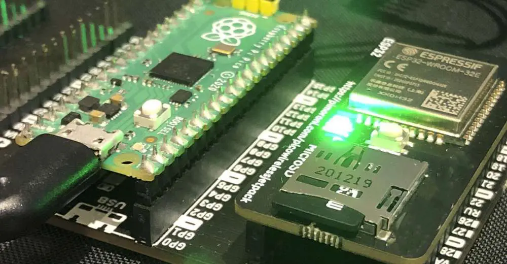
Suppose you’re considering investing in a new chip. In that case, you may be considering the IoT platform from Espressif Systems (Shanghai) Co., Ltd. Espressif Systems (Shanghai), Co., Ltd. (ESS) is a technology company that designs and sells wireless fidelity microcontroller unit communication chips and modules. It also provides software and operating systems to support its chip products. The company has headquarters in Shanghai, China. Its products include smart home appliances, servers, and wireless fidelity communication chips.

The ESPRESSIF Systems Company in China is a technology company with tens of thousands of clients worldwide. Clients range from everyday electronics manufacturers to smart city solutions. The company has offices in India, Brazil, Czech Republic, and Singapore, with most employees in China and India. There is a small team in Singapore. As a company with a global presence, Espressif takes its environmental responsibility seriously.

The company’s products have received praises for their high quality and affordability. The company offers a variety of wireless solutions including Bluetooth, WiFi, and cellular. These systems can help wirelessly connect devices, share files, and make calls. In addition, Espressif is a leader in developing Wi-Fi-enabled products, including wireless Bluetooth technology. The company’s products also feature a variety of innovative features.

Espressif’s IoT platform is open-source

Developers have had a lot of success with Espressif’s IoT platform thanks to its open-source nature. The company’s IoT software development platform, ESP-IDF, has been the basis of many third-party projects. This is a testament to the company’s commitment to democratizing technology. Over 4,000 companies now use its devices.

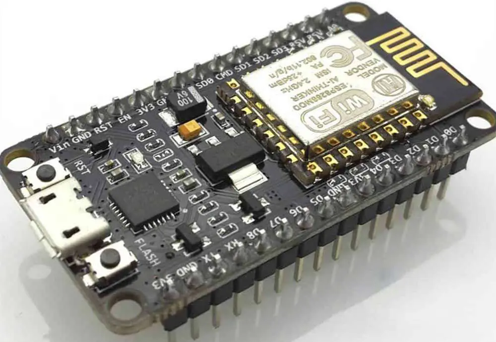
NodeMCU is an open-source IoT platform that combines a Wi-Fi SoC and hardware based on the ESP8266 module. It uses the Lua scripting language and is built on a version of the Non-OS SDK for the ESP8266. It also uses several open source projects to build its core applications. The company aims to make the NodeMCU platform open-source to ensure that developers can build on the platform’s extensible functionality and future proofness.

ASR Microelectronics Company

ASR Microelectronics Company Limited is a semiconductor design company founded in 2015 by Vincent Tai, who previously served as the CEO of RDA.. It engages in R&D and manufactures wireless communication chips. The company focuses on the design of chips for mobile intelligent communication terminals, Internet of Things (IoT) devices, navigation systems, and consumer electronics platforms. This company produces semiconductors for smartphones and other mobile devices. The company has raised more than $330 million in funding. In the past few years, it has been a successful company with a growing number of clients in the U.S., Europe, and Asia.

ASR Microelectronics Company Ltd is a platform chip company

Its main products include cellular baseband chips for mobile phones, multi-protocol non-cellular IoT chips, and artificial intelligence chips. The company provides chip customization services as well. Its target market includes the mobile phone, industrial, and consumer electronics industries.

The company offerings include a smartphone with a 10-core CPU, 4K2K video, 21M camera, and a 5 mode modem with Cat.6. Its target markets include mobile intelligent communication terminals, navigation systems, consumer electronics chips, and multi-standard communications standards.

It acquired Marvell MBU in 2017

ASR Microelectronics Company Limited in China acquired Marvell MBU in 2017 to strengthen its position in the mobile chip market. The deal strengthened ASR’s technological leadership by adding a complete base band platform and a powerful research and development unit. The company will also have access to a strong product program and efficient technical support.

Kangxi Communication Technologies

When looking for the best IT and communications products, you may consider the company Kangxi Communication Technologies. This Chinese firm has developed many original technologies and possesses many advantages over its competitors. These advantages have helped Kangxi Communication compete in the global market and achieve rapid development in the domestic market. The success of the company is inseparable from the efforts of the team. It has also benefitted from continuous enhancement of support for integrated circuits and assistance from cooperative manufacturers.

Founded in 2014, KXcomtech, or Kangxi, is a Chinese company specializing in RF chip design and production. Its staff includes experienced engineers with backgrounds in sales and marketing, product development, and RF front-end. Its patented products include GaAs and CMOS semiconductors. The company also offers a wide range of RF-related products, including RF-modulators, CMOS chip packages, and digital signal processing modules. They have a reputation for excellence and reliability and are constantly developing new products for the market.

We attribute Kangxi Communication’s success in communication equipment to its original technologies and superior products. These factors help the company compete in the international market and make rapid progress in the domestic market. The company’s continuous enhanced support of integrated circuits and help from cooperative manufacturers have contributed to the success of the company.

As an entrepreneur in the WIFI industry, you will be delighted to know that Kangxi Communications has surpassed the global giants in developing and manufacturing RF front-end chips. With an advanced R&D and design methodology, it has become possible to simulate all the components in the WIFI environment, including transistors, capacitors, inductors, package bases, wire connections, and so on.

Telink Semiconductor

The Telink Semiconductor Company is a leading fabless IC design company that designs state-of-the-art wireless connectivity SoCs. Telink has an extensive product portfolio in this area, and is the world’s leading supplier in this field. Its products are useful in various applications ranging from smart lighting to commercial IoT. Its product portfolio also includes low-power, high-precision analog ICs and wearable devices. The products are also useful in other major brands, including Qualcomm, Apple, and other semiconductor and electronics companies.

Radio-frequency and mixed-signal system chips

Chinese fabless semiconductor companies are primarily involved in radio-frequency and mixed-signal system chip design. Telink Semiconductor Company produces radio-frequency chips and system-on-chips.

Telink Semiconductor’s product line includes RF SoCs and low-power wireless chips for consumer electronics, medical devices, industrial IoT applications, audio, smart lighting, wearables, industrial control and home automation applications. Its low-cost ICs make it possible for consumers to afford these devices and systems. The company’s fabless approach has also allowed it to create a large product portfolio. Besides, many other renowned brands use Telink products.

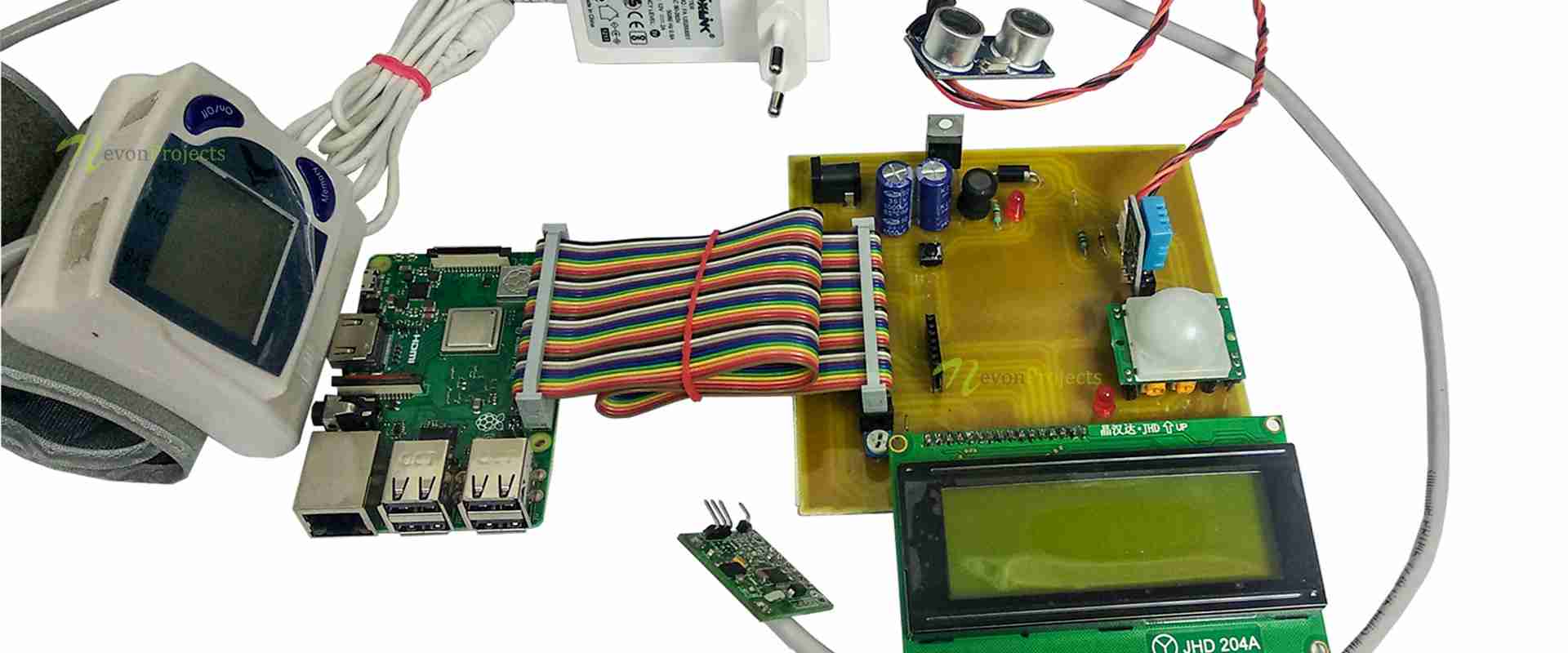
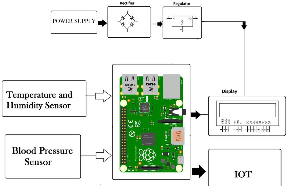
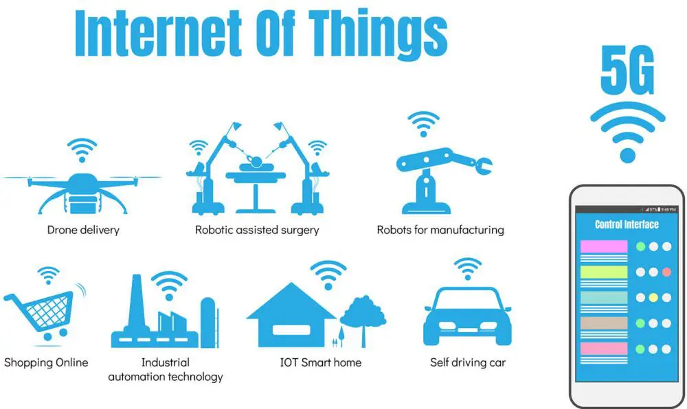
Internet of things (IoT) devices

One of the most important aspects of Internet of Things devices is their ability to transmit and receive data. Traffic lights, for example, are connected to a central traffic control and can either be automated or manually adjusted. Mission control initiate traffic lights that flash amber, and the IoT will make this adjustment automatic. TDL’s One2Touch platform enables continuous communications capabilities, and the Bosch Cross Domain Development Kit (CDDK) simplifies the transition from concept to mass production.

A key component in building an IoT device is an SDK. Telink Semiconductor recently released a Bluetooth wireless SoC for IoT. These devices support Bluetooth SIG mesh specifications and offer unique features, such as automatic synchronization and real-time presence information. The Telink TLSR8269 is the first all-in-one SoC for Internet of Things devices and redefines the landscape. The company offers reference designs and SDKs for developers looking to implement the technology in their products.

Actions

pcb wifi module

Actions Technologies is a high-tech company that integrates scientific R&D, production, and marketing. The company focuses on scientific R&D, engineering service, and marketing. It develops fabless semiconductor products. Its products include SoCs, firmware, and software. They also provide detailed specifications for the rest of the components needed for these products. These products target various applications, including smartphones, wearables, and smart multimedia. Its headquarters are in Zhuhai, China.

The company offers a full range of products and services, and is a complete turnkey solution provider. With highly trained engineers and a responsive service chain, Action specializes in highly customized products. Its facilities contain full installation, testing, and maintenance tools. The team also provides remote technical support.

Its products

A leading fabless semiconductor design company in China, Actions Technology Company Ltd provides mobile internet and multimedia solutions. In addition to SoCs, the company also designs software and firmware and provides detailed specifications for other components needed for a complete product. The company provides total product solutions and an open-source reference design platform to help customers introduce customized solutions quickly. Founded in 2000, the company employs more than 600 people across various divisions.

The company has 20 years of design experience and 230 patents in its portfolio. They strive to provide excellent sound quality products while consuming less power and latency. The company also takes a strong environmental stance, so all of their products comply with leading environmental regulations. Actions Technology’s products meet customer demands and applications, including smartphones, smartwatches, Bluetooth speakers, and mobile phone chargers.

While Actions Technology Company Ltd’s products aim low power consumption, these companies also focus on designing high-quality analog circuits and multimedia products. Their IP focuses on Bluetooth communication, ADC/DAC, high-speed analog interface, and audio processing. In addition to these products, the company also designs high-volume integrated chips and mobile multimedia devices. The company also has a rich multimedia research and development background, having developed audio and video processing solutions for customers globally.

Zhuhai Jieli Technology Company Ltd

IC design and manufacturing company with headquarters in Zhuhai, China, Jieli Technology is a major supplier of Bluetooth audio, BLE, health technologies, and video processing chips. Jieli is a world leader in Bluetooth chips and is in many portable audio products, including TWS earbuds. Jieli also offers Bluetooth solutions for various devices, including smartphones.

The company specializes in developing and manufacturing system-on-chip and other chip products for wireless and mobile communication systems. It offers a wide range of products including 2G/3G/4G mobile communication baseband chips, RF chips, TV and image sensor chips. It also offers one-stop service, including designing, developing and producing chips for Internet of Things (IoT) applications.

The physical design of an IC starts with the creation of the chip’s physical elements on a silicon wafer. The “floor plan” of the chip, used as a blueprint during the process defines the chip’s functions, inputs and outputs. After designing the chip, you place the final circuit elements onto the silicon substrate, ready for fabrication. The process involves custom layout techniques, including using an IC layout editor tool.

Bluetrum Technology

As a semiconductor company, Bluetrum Technology Ltd. in Shenzhen, China, is engaged in developing wireless audio SOC chips for mobile devices. Its products include Bluetooth speaker chips, IoT chips, non-TWS Bluetooth headset chips, flash memory, microprocessors, integrated circuits for quantum computing, artificial intelligence, and OLED displays. Founded in 2016, the company was recently inducted into the 1 Expert Collection of the Shanghai Stock Exchange. In addition, it also develops a range of other technologies including optical storage, wireless audio equipment, WiFi Bluetooth smart chips, computer hardware, battery management, and advanced semiconductors.

Zhongke Lanxun chip products

The company has been focusing on R&D and design of audio chips for high-end headphones and speakers. Its chip products are widely useful in applications such as AI intelligence, smart homes, the Internet of Everything, and other high-tech products. Customers include Lenovo, Sony, Philips, Tmalle Elf, and others. The companyโ€™s products are highly flexible and cost-effective.

Zhongke Lanxun chips and products have many Chinese names. These chips are made of a high-quality silicon and are available in several colors. In addition to this, they are good for both indoor and outdoor use.

Yichip Microelectronics

The Yichip Microelectronics Company is one of the leading semiconductor enterprises in China. It is a full-chain integrated semiconductor enterprise focusing on manufacturing and service. The Company is also capable of developing products and manufacturing processes independently. Its manufacturing process and product technology capabilities are superior, and it has a diverse product range. With a history of more than 10 years, the Yichip Microelectronics Company is a promising investment opportunity.

The Company is a leading semiconductor enterprise in China. The company specializes in designing and manufacturing integrated circuits and other semiconductor components. It also manufactures and distributes quartz crystal components. It has been one of China’s top 100 electronic information enterprises since 2014. Its products are widely useful in various applications, including mobile phones and data-communication systems. Besides, the Company provides consulting services to the semiconductor industry.

Fabless semiconductor companies in China

Chinese fabless semiconductor companies are beginning to emerge, targeting local customers. For example, the Shanghai-based Spreadtrum Communications Company designs chips for mobile phones. HiSilicon Technologies is a captive supplier of Huawei and the largest domestic semiconductor company in China. Combined, these three companies generate a US$6 billion annual revenue, up from $2.8 billion in 2007.

Fabless semiconductor companies don’t make the silicon wafers but outsource the fabrication process to other manufacturers. This method enables semiconductor companies to invest in research and development, while maintaining high production volumes. The semiconductor industry is experiencing a booming market. According to the Semiconductor Industry Association, global sales of semiconductor products topped $470 billion in 2018. Although growth was slower in the second half of last year, it still represents a significant percentage of the chip industry.

Intelligent sensors

In the Internet of Things world, smart sensors are the system’s lifeblood. These devices are becoming increasingly commonplace; nearly anything can have a unique identifier and a way to transmit data. We can implement smart sensors as individual devices or components of a wireless sensor and actuator network. Such networks can be as large as many thousands of sensors connected, or as simple as one or two actuators.

With the help of intelligent sensors, manufacturers can gain deeper insights into the physical world. With the help of these devices, companies can improve operational costs and increase efficiency by leveraging the full range of data they gather. Moreover, they can optimize the use of assets and boost demand planning. The world’s smart sensor market is bound to grow 19 percent annually. We can attribute this growth to technological advancements and miniaturization of devices. Companies can also use smart sensors to drive efficiency, cut costs, and increase revenue through their supply chains.

What is Satisfactory Circuit Board?

Shengyi S1600 pcb

Satisfactory features many recipes, which require supercomputers or computers. Therefore, unlocking them as well as gathering some resources in order to help craft them is very important.

Furthermore, computers are important for the crafting of different end game and middle products in Satisfactory. However, there is a need to unlock them and build them first. It is possible to unlock the initial three computers after you reach tier 5, while Supercomputers could be unlocked later on immediately the Tier 7 is made available.

The circuit board used here is known as a mid-game component that is useful in crafting computers, as well as mid to late game products. Computers have now become an important resource in Satisfactoryโ€™s later stages. This is due to the fact that they are needed for some advanced products and certain buildings. One component which you can craft with the use of computers is the supercomputer.

This leads to a more advanced electronics equipment with time. For instance, there is a need to make use of Supercomputers if you need to utilize Geothermal Generators or Nuclear Power Plants as a source of power or power source.

The different resources in Satisfactory and advanced electronics are available, which are necessary for crafting computers. The three main types of computers usually need different resources for crafting. These include coffee stain studios. However, all these resources require a circuit board.

You can unlock this circuit board in the Oil Processing section of Tier 5. Furthermore, there is a need for four plastic and two copper sheets. The other necessary components useful in crafting the usual computer ought to be obtained easily.

All Types of Computer in Satisfactory and Ways of Building Them

FULL PCB MANUFACTURING Quote

Three major types of computers exist, which could be unlocked at the Tier 5. Also, all of them are useful in the crafting of recipes.

It is possible to interchange these computers in crafting, therefore, it is advisable that players produce the one which they can easily make with respect to the available resources. You can either build these computers at the Manufacturer using the coffee stain studios, which helps in combining 3 or 4 resources. It could also be the assembler that can combine just two.

Also, these computers are useful in crafting vehicles, coupled with different advanced products. This is possible with the help of the circuit board of satisfactory. Supercomputer is an item which you can craft using computers. This gives early access to players to craft more advanced products.

Crystal Computer

This is also in tier 5. Here, you will need three crystal oscillators and eight circuit boards in building a crystal computer making use of the Assembler. Furthermore, the production of crystal computers is done thrice in every 64 seconds.

Computer

This is in tier 5. When creating this form of circuit board Satisfactory Computer, you need nine cables, 52 screws, 18 plastics, and 10 (ten) circuit board. You can build this with the help of the manufacturer. The production of a computer happens once in 24 seconds.

Caterium Computer

This is tier 5. The creation of the Caterium computer is done with the help of the manufacturer and the Caterium circuit board. This is possible using 12 rubber, 28 quickwires, awesome sink, and 7 circuit boards (Caterium circuit board). For the production of Caterium computer, you can produce one in every sixteen 16 seconds.

All the Recipes Using Computers In Satisfactory

Adaptive control unit

This adaptive control unit is usually unlocked in the circuit board of Satisfactory. The manufacturer also crafts it making use of ten circuit boards, fifteen automated wiring, two computers, as well as two very heavy modular frames. In order to create two adaptive control unit (ACUs), it will take about 120 seconds.

Fluid Freight Platform

This requires two computers, 25 cables, 50 concrete, circuit board, 5 motors, 6 modular frames as well as 5 motors. Also, this can be crafted making use of the Build Gun.

Electric Locomotive

Making use of the build gun, it is possible to craft the electric locomotive with about five modular frames, five computers, fifteen steel pipes, five beacons, and ten motors.

Fuel Generator

Here the circuit board of Satisfactory makes use of the build gun in placing a fuel generator. This is twice the amount usually crafted with the use of five computers, 50 rubber, fifteen motors, circuit board, 50 quickwires, and ten modular frames.

Freight Platform

These include two computers, 25 cables, 50 concrete, 6 modular frames, and circuit board are useful in the crafting of the freight platform using the build gun.

Hover Pack

This is in tier 7. It requires eight motors, eight computers, four modular frames, and forty Aluminum sheets are useful in crafting the Hover Pack through the Equipment Workshop.

All the Supercomputer Crafting Recipe Present In Satisfactoryโ€™s Circuit Board

Geothermal Generator

Using the build gun, it is possible to craft the geothermal generator making use of forty copper sheets, sixteen high speed connector, sixteen modular frames, eighty rubber, and 8 supercomputers.

Assembly Director System

This is seen in Tier 7. It is possible to produce one director system every eighty seconds with the help of the assembler, coupled with two ACUs and a supercomputer

Miner MK.3

This is tier 8. And it requires fifty steel pipes, 3 portable miners, 5 supercomputers, 3 turbo motors, and ten modular frames. Others here include the nuclear power plant, particle accelerator, and the programmable splitter.

How to Place the Circuit Board Assemblers In Satisfactory

Here describes the placing of the seven circuit board assemblers on the fifth row. Copper sheet and plastic will help in feeding these. There is a need to directly place one splitter in the copper sheet last merger in that copper sheet that merges the line in the 12th column. There is also a need for copper wire.

The next step is placing a circuit board assembler down to ensure that the initial input stays in line with your splitter. This is necessary so as to connect the conveyor elevator using the splitter. For this stage, you will place the circuit board assembler about three spaces at a distance away from your splitter.

Next, place about six additional assemblers in a specific row towards the left. Then place another splitter onto the ground and ensure that it works with the splitting line of the circuit board assembly. Furthermore, place the splitters that flows to the gridโ€™s left side in-front of each circuit board assemblerโ€™s right input, then connect all the lines.

Conclusion

Hope you now have full details concerning the circuit board of satisfactory. Any questions? Please let us know.

What is Electrical Testing (E-test) in a PCB?

Assembly Testing

Ensuring the stable and consistent functionality and reliability of Printed Circuit Boards (PCBs) is essential. PCB electronic testing is a critical component of the manufacturing process, as it helps identify potential issues and prevents costly failures. In this comprehensive guide, we will examine the various methods used to test and characterize PCBs, offering valuable insights for engineers, manufacturers, and electronics enthusiasts alike.

What is PCB Electrical Testing?

PCB electrical testing is a critical quality control measure in the manufacturing of printed circuit boards. It involves a series of tests designed to verify the electrical integrity and functionality of a PCB before it is integrated into a final product. The primary goal of PCB electrical testing is to identify any defects, shorts, opens, or other electrical issues that could compromise the performance or reliability of the circuit board.

Electrical testing is typically performed after the PCB has been fabricated and before components are mounted. This stage is crucial as it allows manufacturers to detect and rectify any issues early in the production process, saving time, resources, and potential headaches down the line.

YouTube video

The importance of PCB electrical testing cannot be overstated. It ensures that each board meets the specified electrical requirements and functions as intended. By identifying and eliminating defective boards early, manufacturers can:

  1. Improve overall product quality
  2. Reduce production costs associated with rework and repairs
  3. Enhance customer satisfaction by delivering reliable products
  4. Meet industry standards and regulatory requirements

Now that we understand the basics of PCB electrical testing, let’s explore the various types of tests that are commonly performed.

PCB Electrical Testing Types

There are numerous types of electrical tests that can be conducted on PCBs, each designed to evaluate different aspects of the board’s electrical characteristics. Here are some of the most common types of PCB electrical testing:

1. Capacitance Testing

Capacitance testing is essential for evaluating the ability of a PCB to store electrical charge. This test measures the capacitance between different points on the board, ensuring that it falls within the specified range. Proper capacitance is crucial for timing circuits, filtering, and other applications where charge storage is important.

Key points of capacitance testing include:

  • Verifying capacitor values and tolerances
  • Identifying parasitic capacitance issues
  • Ensuring proper impedance control in high-speed circuits

2. Resistance Testing

Resistance testing is fundamental in PCB electrical testing. It measures the resistance between various points on the board to ensure that connections are properly made and that there are no unwanted shorts or opens. This test is crucial for verifying the integrity of traces, vias, and other conductive elements on the PCB.

Resistance testing helps in:

  • Detecting manufacturing defects such as broken traces or incomplete vias
  • Verifying the correct resistance values of embedded resistors
  • Identifying potential issues with solder mask or other insulating materials

3. Comparative Testing

Comparative testing involves comparing the electrical characteristics of a PCB under test with those of a known good board. This method is particularly useful when dealing with complex or custom designs where absolute measurements may be difficult to interpret.

Benefits of comparative testing include:

  • Quick identification of deviations from expected performance
  • Reduced need for extensive test programming
  • Ability to catch subtle issues that might be missed by other testing methods

4. Continuity Testing

Continuity testing is a fundamental PCB electrical test that checks for the presence of a complete electrical path between two points. This test is crucial for ensuring that all intended connections are properly made and that there are no open circuits.

Continuity testing helps in:

  • Verifying proper connections between components and layers
  • Identifying manufacturing defects such as broken traces or incomplete plated-through holes
  • Ensuring the integrity of ground and power planes

5. Flip Test

The flip test is a specialized PCB electrical test used to verify the proper orientation of components on double-sided boards. It involves testing the board in both orientations to ensure that components are correctly placed and that there are no issues with mirrored layouts.

Key aspects of the flip test include:

  • Detecting reversed component placements
  • Verifying proper connections on both sides of the board
  • Identifying potential issues with through-hole components

6. Clamshell Testing

Clamshell testing is a method of PCB electrical testing that uses a fixture with two halves that close around the board like a clamshell. This technique allows for simultaneous testing of both sides of the PCB, improving efficiency and reducing test time.

Advantages of clamshell testing include:

  • Faster testing of double-sided boards
  • Improved contact reliability due to even pressure distribution
  • Ability to test boards with components on both sides

7. Adjacency Testing

Adjacency testing focuses on verifying that there are no unintended electrical connections between adjacent traces or pads on a PCB. This test is particularly important for high-density boards where the risk of shorts due to manufacturing defects is higher.

Adjacency testing helps in:

  • Detecting potential short circuits between closely spaced traces
  • Identifying issues with solder mask or other insulating materials
  • Ensuring proper isolation between different circuit sections

8. Flying Probe Testing

YouTube video

Flying probe testing is a flexible PCB electrical testing method that uses movable probes to make contact with specific points on the board. This technique is particularly useful for testing prototype or low-volume PCBs where the cost of a dedicated test fixture may not be justified.

Key features of flying probe testing include:

  • Ability to test complex boards with minimal setup time
  • Flexibility to accommodate design changes without modifying test fixtures
  • High precision and ability to test fine-pitch components

9. PCB Stress Testing

PCB stress testing involves subjecting the board to various environmental and electrical stresses to evaluate its performance under extreme conditions. This type of testing helps ensure that the PCB can withstand the rigors of its intended operating environment.

Common PCB stress tests include:

  • Thermal cycling to simulate temperature variations
  • Vibration testing to assess mechanical durability
  • Power cycling to evaluate the board’s response to repeated on/off cycles

10. In-Circuit Testing

In-circuit testing (ICT) is a comprehensive PCB electrical testing method that evaluates individual components on a populated board. This test uses a bed-of-nails fixture to make contact with numerous test points simultaneously, allowing for rapid and thorough testing of complex assemblies.

Benefits of in-circuit testing include:

  • Ability to test both passive and active components
  • Detection of manufacturing defects such as solder bridges or missing components
  • Verification of component values and basic functionality

11. Functional Testing

Functional testing is the final stage of PCB electrical testing, where the assembled board is evaluated under conditions that simulate its intended use. This test verifies that the PCB performs all its required functions correctly and meets the specified performance criteria.

Key aspects of functional testing include:

  • Verifying proper operation of all circuit functions
  • Testing board performance under various input conditions
  • Evaluating the interaction between different subsystems on the PCB

12. Burn-In Testing

YouTube video

Burn-in testing is a reliability test that involves operating the PCB under elevated stress conditions (such as high temperature or voltage) for an extended period. This test is designed to identify any early-life failures or “infant mortality” issues before the product is shipped to customers.

Burn-in testing helps in:

  • Identifying weak components or manufacturing defects that might lead to premature failure
  • Improving overall product reliability
  • Reducing the likelihood of field failures during the product’s early life

Methods of PCB Electrical Testing

Now that we’ve explored the various types of PCB electrical testing, let’s delve into the methods used to perform these tests. There are several approaches to PCB electrical testing, each with its own advantages and applications.

1. E-test Method 1: Flying Probe Testing (FPT)

Flying Probe Testing, also known as FPT, is a versatile and widely used method for PCB electrical testing. This technique employs movable probes that can be positioned anywhere on the board’s surface to make electrical contact with test points.

Key features of Flying Probe Testing include:

  • Flexibility: FPT can easily adapt to different board designs without the need for custom fixtures.
  • Cost-effectiveness: Ideal for low-volume production or prototype testing where dedicated fixtures may not be economical.
  • Precision: Capable of testing fine-pitch components and densely populated boards.
  • Minimal setup time: New boards can be programmed and tested quickly.

The FPT process typically involves the following steps:

  1. Board alignment and registration
  2. Probe movement and contact with test points
  3. Electrical measurements and data collection
  4. Analysis and reporting of test results

While FPT is slower than fixture-based testing for high-volume production, its flexibility and low setup costs make it an excellent choice for many PCB manufacturers.

2. E-test Method 2: Fixture Method

The fixture method, also known as bed-of-nails testing, is a high-speed PCB electrical testing technique that uses a custom-designed test fixture with numerous spring-loaded pins (the “nails”) to make contact with specific points on the board simultaneously.

Advantages of the fixture method include:

  • High-speed testing: Ideal for high-volume production
  • Comprehensive coverage: Can test hundreds or thousands of points simultaneously
  • Repeatability: Consistent results due to fixed probe locations
  • Durability: Fixtures can withstand thousands of test cycles

The fixture method process typically involves:

  1. Designing and manufacturing a custom test fixture for the specific PCB
  2. Loading the PCB into the fixture
  3. Applying pressure to ensure good contact between the board and test pins
  4. Performing a series of electrical tests
  5. Analyzing and reporting the results

While the initial cost of creating a custom fixture can be high, this method becomes very cost-effective for large production runs where the setup cost is amortized over many boards.

3. PCB Testing During Manufacturing

PCB electrical testing is not a single-step process but rather an integral part of the entire manufacturing workflow. Testing occurs at various stages to ensure quality and catch defects as early as possible.

Key testing stages during PCB manufacturing include:

  1. Bare board testing: Performed after PCB fabrication but before component assembly
  2. In-circuit testing: Conducted after components are mounted but before final assembly
  3. Functional testing: Performed on the fully assembled PCB

Each stage of testing serves a specific purpose and helps to maintain high quality standards throughout the production process.

4. Mechanical PCB Testing and Inspection

While not strictly part of electrical testing, mechanical testing and inspection are crucial components of overall PCB quality assurance. These processes ensure that the physical characteristics of the board meet specifications and that there are no visible defects.

Mechanical PCB testing and inspection may include:

  • Dimensional verification: Checking board size, hole diameters, and component placement
  • Visual inspection: Looking for visible defects such as scratches, dents, or misaligned layers
  • X-ray inspection: Examining internal layers and hidden solder joints
  • Microsectioning: Analyzing the internal structure of the PCB

These mechanical tests complement electrical testing to provide a comprehensive quality assessment of the PCB.

5. Electrical PCB Testing During Manufacturing

Electrical testing during the PCB manufacturing process is a multi-stage approach that ensures the quality and functionality of the board at each critical step. Here’s a closer look at how electrical testing is integrated into the manufacturing workflow:

  1. Bare Board Testing:
    • Performed after PCB fabrication but before component assembly
    • Checks for opens, shorts, and correct impedance on traces
    • Verifies the integrity of plated-through holes and vias
    • Ensures proper isolation between layers
  2. Component Placement Verification:
    • Conducted immediately after component placement but before soldering
    • Uses optical or X-ray inspection to verify correct component orientation and placement
    • Helps prevent issues caused by misplaced or missing components
  3. Post-Reflow Testing:
    • Performed after components are soldered to the board
    • Checks for solder bridges, cold joints, and other soldering defects
    • May include thermal imaging to identify potential hot spots
  4. In-Circuit Testing (ICT):
    • Conducted on the assembled board
    • Tests individual components for proper values and basic functionality
    • Identifies manufacturing defects such as shorts, opens, or incorrect components
  5. Functional Testing:
    • Performed on the fully assembled PCB
    • Verifies that the board functions as intended under various operating conditions
    • May include power-on testing, signal integrity analysis, and performance benchmarking
  6. Final Quality Assurance:
    • Combines results from all previous tests
    • May include additional environmental stress testing or burn-in procedures
    • Ensures that only fully functional and reliable PCBs are shipped to customers

By incorporating electrical testing throughout the manufacturing process, PCB producers can identify and address issues at the earliest possible stage, minimizing rework costs and improving overall product quality.

Why Electrical Testing Is Crucial and How It Matters to You

PCB electrical testing is not just a technical requirementโ€”it has far-reaching implications for manufacturers, customers, and end-users alike. Understanding the importance of thorough electrical testing can help you make informed decisions about your PCB projects and ensure the success of your electronic products.

1. Quality Assurance

Electrical testing is the backbone of PCB quality assurance. It provides objective data on the performance and reliability of each board, ensuring that only high-quality products reach the market. For manufacturers, this means:

  • Reduced warranty claims and returns
  • Enhanced reputation for reliability
  • Improved customer satisfaction and loyalty

For customers and end-users, rigorous electrical testing translates to:

  • More reliable electronic products
  • Longer product lifespans
  • Reduced frustration from malfunctioning devices

2. Cost Savings

While electrical testing does add to the initial production cost, it ultimately leads to significant cost savings:

  • Early detection of defects reduces costly rework and scrap
  • Fewer field failures mean lower warranty and support costs
  • Improved yield rates lead to more efficient production

These savings can be passed on to customers in the form of more competitive pricing or reinvested in product development and innovation.

3. Regulatory Compliance

Many industries have strict regulatory requirements for electronic products. Comprehensive electrical testing helps ensure that PCBs meet these standards, which is crucial for:

  • Obtaining necessary certifications (e.g., UL, CE, FCC)
  • Entering regulated markets (e.g., medical devices, aerospace)
  • Avoiding legal issues and potential recalls

4. Product Performance and Reliability

Thorough electrical testing contributes to improved product performance and reliability:

  • Identifies potential weak points before they become field failures
  • Ensures consistent performance across production batches
  • Helps in fine-tuning designs for optimal performance

For end-users, this means products that work as expected and continue to perform reliably over time.

5. Time-to-Market

While it might seem counterintuitive, investing in comprehensive electrical testing can actually speed up time-to-market:

  • Catches design issues early in the development process
  • Reduces the likelihood of last-minute design changes
  • Streamlines the certification process

This can give manufacturers a competitive edge in fast-paced markets where being first to market is crucial.

6. Continuous Improvement

The data gathered from electrical testing is invaluable for continuous improvement efforts:

  • Identifies trends in manufacturing defects
  • Provides insights for refining design guidelines
  • Helps in optimizing production processes

For customers, this ongoing improvement translates to ever-increasing product quality and reliability.

PCB Electrical Testing at RAYMING PCB

At RAYMING PCB, we understand the critical importance of thorough and accurate electrical testing in the PCB manufacturing process. Our state-of-the-art testing facilities and experienced technicians ensure that every board we produce meets the highest standards of quality and reliability.

Our Comprehensive Testing Approach

  1. Advanced Testing Equipment:
    • We utilize cutting-edge flying probe testers for flexible, high-precision testing
    • Our bed-of-nails fixtures provide rapid, comprehensive testing for high-volume production
    • Thermal imaging and X-ray inspection systems complement our electrical testing capabilities
  2. Customized Testing Solutions:
    • We develop tailored testing protocols based on your specific PCB design and requirements
    • Our engineers work closely with you to identify critical test points and parameters
  3. Multi-Stage Testing:
    • We perform electrical tests at every crucial stage of the PCB manufacturing process
    • From bare board testing to final functional verification, we ensure quality at every step
  4. Data-Driven Quality Assurance:
    • Our advanced data analytics help identify trends and potential issues before they become problems
    • We provide detailed test reports with each order, giving you complete visibility into the quality of your PCBs
  5. Continuous Improvement:
    • We regularly review and update our testing procedures to stay ahead of industry standards
    • Our team undergoes ongoing training to maintain expertise in the latest testing methodologies

What is FR4 Tg PCB?

Isola FR406N PCB

As electronic technology continues to develop, there is a high demand for high Tg boards.Furthermore, glass transition temperature (Tg) is a very important property of an epoxy. Also, this temperature region is one whereby the base material, which is either glass or polymer changes from its glassy, rigid, solid state into a rubbery state.

All PCB features a unique Tg value which is usually based on the substrate. Furthermore, PCB will begin to alter its state. This affects the PCB fabrication process wrongly if the PCBโ€™s operating temperature surpasses its Tg value. In addition, the PCB boards with high Tg usually feature better stability whenever there are high temperatures. This is due to the fact that the substrate offers better chemical and mechanical stability, and heat resistance for the board.

Therefore, your Tg value must fall within 20 and 25 degrees centigrade more compared to the operating temperature of that device expected for the board to be useful in selecting a PCB.

What Does FR4 Mean?

Printed circuit boards usually make use of composite material glass fabric as well as a flame retardant made of epoxy resin.

This reinforcing material of 4th grade is useful in PCB boards to help in resisting a more glass transition temperature. Also, the presence of this substrate in the PCB is significant, such as printed circuit boards (PCBs) present in the electrical machines.

FR means fire retardant material. Majority of PCB manufacturers make use of FR4 as a result of its consistent mechanical and physical properties. In addition, the FR4 laminates are board materials with epoxy pigment useful in enhancing the integrity of the circuit board.

What does High TG PCB Mean?

Base material, either glass or polymer, is shifting from its rigid, solid, glassy state to a rubbery state whereby the temperature rises to a specific area. The temperature here is referred to as the glass transition temperature(Tg). What we mean is that Tg is known as a mechanical property, which designates the glass transition temperature. This temperature is one at which this substrate stays rigid.

What are the Properties of the Fr4 Tg PCB?

FULL PCB MANUFACTURING Quote

The use of materials of high Tg PCB is becoming higher in the global electronics industry. The usefulness of these high Tg PCBs can be seen in communication equipment, control panels, and computers.

The major difference here is the high prices. This is because these high Tg fr4 PCBs are more expensive than the usual Tg PCBs. Furthermore, these high Tg material feature most of the important properties. These include:

  • Adhesion
  • Better strength and mechanical property
  • Stronger moisture resistance and water absorption
  • Stability in its dimensions
  • Thermal decomposition during any hot condition
  • Chemical resistance
  • High heat resistance or higher heat resistance
  • More resistance to any thermal stress
  • Longer durability for the PCB laminates
  • Reliable and efficient PTH
  • Lower CTE (coefficient of thermal expansion) at the Z-axis

What are the Benefits of a High Tg PCBs?

Greater stability: This automatically improves the chemical resistance, heat resistance, moisture resistance, temperature resistance and the deviceโ€™s stability by raising the temperature of glass transition (Tg) of a specific PCB substrate.

It bears designs with high power density: A high Tg PCB serves as a very good solution for all heat management. This holds if that device features high power density as well as a high heat generation rate.

Also, with the use of the larger PCB (printed circuit board) in changing a deviceโ€™s power and design requirements when reducing an ordinary boardโ€™s heat generation. In addition, it can also make use of high Tg PCB (Printed circuit board).

Great for HDI and multilayer PCBs: This can cause high heat dissipation levels. This is due to the fact that the HDI and multilayer PCBs feature dense circuits and are usually more compact. Therefore, the high Tg PCBs are usually useful for the HDI and multilayer PCBs. This ensures reliability during PCB fabrication

Reasons why Using the high Tg PCB is Necessary

Note that if yourPCB (printed circuit board) canโ€™t bear the thermal load that is not having a Tg value that is 25 degrees centigrade less than the usual Tg, then there is a need for a high Tg PCB (Printed circuit board)to work with your applications.

Furthermore, it ensures the safety with your high Tg PCB if the product operates at a range of 130 degrees centigrade or more. The major reason behind the high Tg PCB is due to the movement onto the RoHS PCB (Printed circuit board). Therefore, there are additional PCB industries that are moving toward the high TG materials because the lead-free solder needed to flow will require higher temperatures.

What are the Applications of High Tg FR4?

Note that when a higher power density is present in electronic products and then heat generation also tends to disturb the heat sink as well as other parts of your products, the most appropriate solution is to using a high Tg FR4 PCB.

Furthermore, youโ€™ll learn that the high Tg FR4 PCBs are usually applied in the electronic industries. These industries can function in high temperatures This is because high Tg FR4 PCB are becoming more popular recently. Top manufacturers like RayMing serve their customers from many different industries. They achieve this by offering high Tg FR4 PCBs having a heat resistance, which meet all the demands as well as the specifications of the customer in the quick lead time.

The following areas are places where the High Tg fr4 is applicable:

  • Rfid
  • Gateway
  • Antenna
  • Inverter
  • Embedded systems development
  • Contract manufacturing services
  • WiFi Booster
  • Low Cost Plc
  • AC power supplies
  • Embedded Computer Systems

Conclusion

When designing, one important feature to look into when identifying PCBs is the high Tg. Furthermore, it is necessary to pick the material with respect to the usage. This refers to the low working or high temperature requirements. Other things to consider include the thermal expansion, electrical properties, temperature resistance, mechanical and electrical properties, high temperatures, and higher heat resistance or high heat resistance. Any questions? Please notify us.

How BT PCB is Contributing to the Advancement in Electronic Equipment

bt pcb

BT stands for bismaleimide triazine. This laminate sheet has impacted the chip packaging industry. Chip packaging is crucial in PCB assembly. Laminated materials for circuit boards usually comprise several layers of impregnated and dried glass fiber cloth pressed onto the chip substrate. However, a thermal-hardened bismaleimide triazine (BT) resin material was introduced. This material offers great electrical and thermal properties and is low cost.

BT resin laminate has been playing a crucial role in the development of electronic equipment and information technology.

What is a BT PCB?

BT stands for bismaleimide triazine. ย It is one of thermoset resins utilized in manufacturing PCBs. Also, this component is a primarily a mixture of epoxy resin and BT resins. The epoxy resin is a common raw material used for PCBs. Also, the BT resins are majorly a mixture of bismaleimide, used as a common raw material for circuit boards and cyanate ester. BT resin is a combination of strongly basic molecules.

BT resin features great properties like excellent electrical properties and high thermal resistance.  These features increased the standard for high-performance semiconductors. Also, the low cost of BT laminate makes it an ideal option for chip packaging. Therefore, BT laminate is contributing to technological advances for electronic devices.

To date, BT laminate remains a good standard for chip packaging. Before the introduction of BT laminate, the laminate used for high-performance chips was high-cost ceramic. However, BT became an alternative with great electrical and thermal properties. When the chip manufacturing industry noticed this material, the BT resin was used for chip packaging in 1985.

This material became to gain acceptance in Japan and across the world when the chip manufacturing industry accepted the cost savings. Furthermore, BT resin made the chip fabrication process much simpler. To date, BT resin is a popular laminate material for chip packaging. BT PCB is a mixture of epoxy resin and bismaleimide.

Applications of BT PCB

Any devices featuring electronic components feature one or more computer chips. Device makers constantly look for how to make their products better by making them lighter and smaller. Also, they make these devices more sophisticated.  An example of this is the smartphone technology that keeps evolving each model while becoming more powerful, lighter, and more versatile.

The manufacturers of the chips in these devices keep improving their chip technology to meet the demands of manufacturers for advanced functionality. Also, chip manufacturers need to put more parts into a chip to make devices lighter and more efficient. Therefore, these manufacturers make use of denser materials that can reduce spacing between the traces.

Spacing of traces has reduced from more than 100 microns to less than 20 microns. Furthermore, the greatest challenge during PCB fabrication is avoiding curvature or deformation caused by temperature variation. Also, PCB fabrication involves processes that alternate cold and hot. Therefore, the chip must comprise materials that must keep their shape in these conditions. The bismaleimide triazine resin is a low cost material that features high performance in all aspects.

Also, chips function under conditions with incessant contraction and expansion. Therefore, they must be able to keep their performance specifications without any form of degradation throughout their life span. The bismaleimide triazine resin is a primary material in chips that function in electronic devices of today.

Also, the complexity of todayโ€™s technology keeps demanding for a dramatic revolution in the semiconductor industry. Bismaleimide triazine resin is the breakthrough these technologies need. Therefore, the industry keeps improving BT laminate and anticipating the future demands of chip makers.

Properties of BT Epoxy

BT epoxy is widely used in fabricating printed circuit boards due to their exceptional electrical and mechanical properties. Also, BT features excellent thermal properties. This laminate is ideal for lead-free PCB assembly. Also, BT epoxy resin is primarily used in multilayer PCB applications. BT epoxy offers great features like high heat resistance, exceptional electromigration, and insulation resistance.

Furthermore, BT epoxy features high bond strength at extremely high temperatures. BT epoxy resin is widely used across several industries since they offer a great level of protection.  BT epoxy is listed in some standards in the world due to its properties.  For example, IPG4101-1997 listed it as โ€œNo. 30โ€ board while EC 249-2-1994 listed it as โ€œ18โ€ board

In addition, BT epoxy features a high glass transition temperature and low dielectric constant. Therefore, BT resin substrate can improve the interconnection of printed circuit boards. BT stands for Bismaleimide triazine. This common raw material features low thermal expansion and exceptional dielectric properties. Therefore, this makes it ideal for high-density interconnect (HDI).

The properties of BT epoxy includes:

  • Exceptional thermal shock resistance
  • Great ion migration resistance
  • Exceptional dielectric performance, Dk is within 2.8 and 3.5
  • Great electrical properties
  • Excellent dimensional stability and curing shrinkage
  • Good wettability and low melt viscosity

Factors that Determine the Performance of BT PCB

BT resin as a common raw material for PCB fabrication varies from low-viscosity liquid to solid based on the ratio and variety of CE and BMI. There are several factors determine the performance of BT PCB. These factors include:

Development of lead-free soldering technology

The majority of PCB manufacturer integrate led-free soldering technology. This has become the mainstream of the industry. Higher temperature reflow soldering related with this technology will put more heat resistance requirements on PCB production.

Packaging technology development

Traditional semiconductor packaging products like DIP and QFP should connect the chip to the lead frame and utilize gold wire to link the aluminum pad on the chip. The utilization of organic substrates with internal pin, connection PBGA, EBGA, and packaging methods like TAB are increasing. Also, many new technologies like WLSCP, CSP, and chip packaging soil are increasing as portable products need component volume miniaturization.

High frequency

The information and communication technology has enhanced its working frequency. For instance, mobile phonesโ€™ standard has evolved over time. Also, the operating frequency of the CPU has changed over time. The emergence of different digital communications and the development of MHz and now GHz  are part of the development.

Conclusion

BT PCB is highly preferred among electronics manufacturers due to its electrical and mechanical properties. Also, the low cost of BT laminate makes it an ideal option for chip packaging.

How 5G IoT is Changing the Future of Technology

5G IoT Technology

5G has brought several new possibilities for businesses and enterprises that require faster data and more efficiency. The impact of 5G in the technology world and the whole world at large has become so evident. With the increasing production of more advanced electronics, there is need for faster signal transmission and data transfer.

5G is presently available in most cities in the developed world. With 5G, a lot of IoT applications and devices will be connected easily. 5G Internet of Things supports new business models. The mobile communication system has experienced a lot of development in the past years. This system has seen the transformation from 2G to 3G to 4G and now 5G.

In this article, we will provide answers to questions like what is 5G IoT and how exactly does 5G offer greater data speeds?

What is 5G?

5G refers to the fifth-generation cellular technology that enables new capabilities like cloud computing, Internet of Things, Artificial Intelligence, and Edge computing. There are several factors that trigger the integration of 5G and IoT. Some of these factors include the availability of affordable devices and the rising demand from enterprises and consumers.

In addition, the adoption of global standards is driving growth and increasing market interest in the Internet of Things. Edge computing, AI, and cloud computing can handle the volumes of data produced by the IoT. Furthermore, 5G advancements like 5G core and network slicing will help to achieve the goal of a global IoT network.

The transformation in the digital world is basically changing businesses and the society at large. Also, it is changing our daily lives. Mobile networking is the brain behind this transformation. Also, mobile networking offers reliable and global connectivity to over 6 billion mobile devices. 5G is also responsible for high computing power in modern devices.

How Does 5G Benefit IoT?

5G offers many benefits for Internet of Things. Also, faster connection of things can help enterprises and businesses to develop new products or improve existing ones. Furthermore, the impact of IoT keeps growing as it transcends almost every industry like smart manufacturing and utilities, automotive. In addition, Internet of Things will keep benefiting the society at large by enabling government policy implementation.

By enabling the reduction of waste of critical resources like water, the initial mobile networks such as 2G, 3G, and 4G offer the basic foundation for connecting things. These mobile networks were initially designed to ensure mobile broadband and personal communication services. However, they have provided the capability to meet the demands for IoT. Also, they offer technical capabilities beyond most existing use cases.

For instance, global standardization indicate that services and products can be globally scaled. With billions of connected mobiles, there will be reliability, cost efficiency, and the constant development of devices.

Therefore, 5G offers the following key benefits for IoT

  • Faster data in local and urban areas networks
  • Improved mobile broadband
  • Enhanced energy saving functions for indoor devices
  • Very reliable low latency communications
  • Better connectivity for the internet age in rural places

5G is now available across the globe. Also, this 5th generation mobile network is specially designed to support IoT use cases. Therefore, 5G offers dedicated capabilities designed for different kinds of IoT applications. 5G enables the development of new IoT applications. Also, this cellular technology will keep fueling digital transformation. Therefore, this will benefit consumers, enterprises, and the society at large.

Also, 5G offers several benefits to the mobile industry. The mobile communications industry depends on 5G IoT. In addition, 5G helps to ensure efficiency and reliability in most IoT projects.

How 5G Evolution Creates New Opportunities in IoT

As 5G becomes more available, it will offer support to mission critical Internet of Things. This is possible due to the low latency and higher bandwidth provided by 5G. Therefore, this will ensure future use cased like automated guided vehicles, assisted driving, connected devices, and more. Also, it is still not clear how 5G will be needed at the upgrade path to offer support to IoT use cases that require continuous high-speed communications.

5G will offer several new possibilities for business and enterprises that require faster and more efficient data. Also, 5G can address several use cases that require a lot data like video streaming. 5G is available in major cities. In large parts of Europe, this cellular technology will replace both 2G and 3G. The replacement of 2G and 3G with 5G in many European countries is a mainstream reality in the year 2025.

Furthermore, 5G will help IoT applications to gain more remote control. For instance, NB-IoT and LTE-M will enable network functionality that ensures improved coverage or minimized battery consumption for an application. 5G enables mass deployment for simpler and more efficient IoT devices, like sensors. Also, these devices transmit little data. However, energy efficiency, cost, and better coverage can be crucial for relevant use cases.

5G enhanced mobile broadband offers more data. Also, it improves data security. Therefore, it offers fast response which can be widely used collaborative robots and autonomous vehicles. Network edge in IOT project is crucial.

5G Development Stage from an IoT Application Perspective

For the past few years, 5G deployment became rapid in several markets across the world. Also, mobile phones with 5G capability have become more affordable. Therefore, this enables mobile broadband users start gaining 5G benefits where available. This situation is kind of different from an IoT application perspective.

For instance, several IoT use cases require continuous network access. This means the application requires optimizing networks having sufficient coverage. It is crucial to think ahead when it comes to IoT applications. This is because the decision made today will affect the cost and capabilities of the connected devices for several years.

From the perspective of an IoT application, it is better to view the road to 5G in three stages. These stages are transition, evolve, and transform.

Transition stage

FULL PCB MANUFACTURING Quote

5G introduction will be more than a 10 year period. Every network generation needs to be well standardized to enable global interoperability. Also, the regulator in every country plans the award licenses to utilize it. Furthermore, communication service providers need to operate the new network and perform roll outs.

It is a lengthy process when rolling out a new mobile network. Also, it takes years for a new network generation to accomplish the same coverage as the preceding generations. This transition stage will last until the new network offers enough coverage to eliminate dependency on legacy networks. Also, when it comes to international IoT applications, this stage may last until all countries have enough coverage.

The roll-out time for 5G will vary for different use cases. For instance, big mobile IoT capabilities such as NB-IoT and LTE-M are well optimized for a better coverage. IoT application must rely on multiple networks generation to get enough coverage. Therefore, this means the application canโ€™t enjoy full benefit of new network capabilities.

Evolve stage

It will be feasible to start indicating the first benefits from new capabilities as 5G network coverage is sufficient. The demands of the application determine the type of coverage needed. For instance, an application where the communication information isnโ€™t time critical needs less coverage than applications with near real-time characteristics. Based on the location, IoT use cases will get to this stage between now and 2025.

Physical connectivity is one of the first benefits of 5G. Device cost for applications having strict cost requirements will reduce once we eliminate fallback technology and make use of 5G. Also, this can allow new applications that have not been feasible economically. With the help of other 5G characteristics, new and improved applications can be also designed.

As economical and technical limitations relax, there will be more opportunities to innovate new applications. With 5G devices, the feasibility of bringing an โ€œalways-onโ€ user experience for IoT devices is high. Also, 5G technologies make it easy to simplify modern architecture and prepare it for more transformation change.

In several cases, one can directly attach sensors to the mobile network. This helps to enhance operational characteristics.

Transform

IoT application must enable the appropriate characteristics of the network infrastructure to enhance business. For instance, there may be a need to assure response times and data rates. Also, 5G helps the application to see the networkโ€™s capabilities. This enables 5G to support the specific needs of the network by programming it.

Furthermore, this can only work when the desired capabilities are already deployed in the network having enough coverage. It isnโ€™t an easy task to accomplish the vision of 5G. Achieving this vision can take years. However, there are new practical uses cases and more capabilities. Also, accessing low power consumption and improved coverage capabilities is now possible. Therefore, this has paved way for more new use cases.

Furthermore, IoT service providers across the globe are incorporating access to such functionality. The accessibility of 5G capabilities for development project must have been integrated into the services and software used for the application. Furthermore, 5G will result in a long period of transformation in the mobile IoT ecosystem.

Therefore, enterprises that look forward to transforming their business should opt for partners that can support business-critical processes.  Focusing on business challenges and developing the IoT system plays a key role in the future.

5G IoT Use Cases

There are several use cases of 5G IoT. These uses cases include:

Manufacturing

Industrial companies are already leveraging the Industrial IoT to keep track of the location of these assets. With 5G IoT, it is easy to develop smart factories with robotics and AI. The ultra-reliable low-latency 5G helps to reveal transformative use cases in manufacturing and infrastructure systems.

Smart traffic mobility

5G IoT applications can ensure real-time data is shared about road and traffic conditions among road users. This driver assistance services and smart mobility need 5G communication devices in roadside sensors and vehicles. Also, gathering and analyzing real-time  IoT data from vehicles and roadside infrastructure help to warn drivers about any hazardous road conditions. Therefore, traffic efficiency and road safety will improve.

Video survelliance

5G has ensured digital transformation in our todayโ€™s world. One of the IoT applications 5G has enhanced is the video surveillance. The recent events across the globe has triggered governmentโ€™s investment in security systems and public surveillance. Also, video surveillance systems often depend on wired  connectivity.

However, the integration of wireless connectivity can lead to lower costs, providing reliable connectivity and performance. 5G and IoT solutions prevent critical assets loss. With 5G, we can secure and monitor facility conditions properly.

Smart city

According to the European Commission, Smart cities are where traditional services and networks are more efficient with the integration of telecommunication and digital technologies. Smart cities utilize the 5G and IoT devices to gather real-time information. Therefore, this helps to understand the patterns of demands and respond with lower-cost and faster solutions.

Furthermore, 5G will reveal IoT potential and this will be a driving force for smart cities. It will achieve this by addressing and providing solutions to all connectivity issues.

Smart grid automation

Electricity demand is rising. Smart grids and virtual power plants are solutions for this rising demand. With 5G, we can integrate real-time management and ensure smart electricity grid automation. Maintenance optimization can begin once fault is detected. 5G IoT is widely integrated due to the lower latency and increased deployment rate.

Therefore, utility operators are gradually updating their grids with new control systems. Also, smart grid automation can help to get rid of blackouts across the world.

Asset tracking

Remote monitoring with IoT is not new. However, using 5G to secure connectivity helps to deliver great benefits. Asset tracking solutions transmits data from a sensor to the cloud for storage and analysis. 4G LTE networks are compatible with 5G. For instance, NB-IoT is the brain behind 5G massive-Type Communications. The mobile industry requires asset tracking to ensure efficiency.

Remote working and studying

5G has enabled remote studying and working. Improved mobile broadband will allow more mobile data at once. 5G can enable devices with more efficient hardware require a long battery life. Also, longer battery life indicates that devices can transmit data on their location for a long period. The internet is critical in keeping the society connected. An example of this is was the COVID-19 lockdown. During lockdown, remote working and studying became the order of the day.

Conclusion

The impact of 5G in the technology world and the whole world at large has become so evident. Also, there are several use cases of 5G IoT.

Why you Should Use TTM PCB for Your PCB Projects

Shengyi SG7350D PCB

In the technology world, various companies are working towards development. These companies offer high quality services and products. One of such companies is TTM Technologies .Inc. This company is well-known for its positive impact in the PCB industry. We are going to shed more light on the products and services provided by this company. Also, we will give more details on how they operate.

What is TTM Technologies .Inc?

TTM technologies, is a popular and leading global printed circuit boards manufacturer. Also, this leading global printed circuit board manufacturer focuses on delivering quick-turn and high volume production of technically advanced circuit boards. TTM stands or refers to โ€œfor time to market.โ€ Also, TTM Technologies .Inc specializes in manufacturing RF components.

TTM Technologies Inc. has its headquarters in Santa Ana, California. Also, the major focus of this manufacturer is time-to-market. With its advanced technologies, procedures, and services, customers can reduce the time needed to make their advanced electronics available. TTM technologies .Inc dedicates its time to production of advanced circuits, RF and microwave components, and backplane assemblies.

This company is one of the worldโ€™s biggest PCB producers and a large supplier of custom electro-mechanical solutions and backplane assemblies. Also, it offers one-stop manufacturing services that help to shorten production time.   The time-to-market reveals TTMโ€™s time-critical.

TTM Technologies .Inc offers all types of PCB boards like rigid-flex, flex, HDI, and rigid. Also, it offers up to 40 layers circuit boards. This competitive organization works with a team of experienced engineers that offers customers the necessary advice and support. also, TTM Technologies is dedicated to meeting the needs of its customers by continuously improving product quality and customer service.

More Facts about TTM Technologies .Inc

FULL PCB MANUFACTURING Quote

TTM Technologies deals with the manufacturing and sale of printed circuit boards across the world. Also, TTM Technologies. Inc operates in two different segments which are RF components and PCB. This company offers

  • Radio frequency and microwave circuits
  • PCB products
  • Conventional PCBs
  • High density interconnect (HDI) PCBs
  • System integration products
  • Advanced ceramic RF components
  • Radio frequency components
  • Beamforming and switching networks
  • Multi-chip modules

Furthermore, this company manufactures circuit boards with heavy copper cores. Also, it produces electrically passive heat sinks and circuit boards with active thermal cores. TTM Technologies .Inc delivers value added services which include PCB layout design, quick turnaround, and design for manufacturability. Also, it offers services like simulation and testing.

TTM Technologies .Inc has its headquarters in Santa Ana. This company acts as electronic manufacturing services companies and original equipment manufacturers. Therefore, TTM Technologies .Inc serve data center computing, medical, aerospace and defense sectors.

As a leading global printed circuit board manufacturer, TTM Technologies .Inc manufacturing services enable customers to achieve the best PCB project. Also, this company features design capabilities to produce technologically advanced PCBs. This leading global manufacturer has huge net sales. TTM Technologies .Inc delivers specialty components for electronics manufacturing. Also, it delivers high frequency radio frequency components.

TTM stands for time to market. Therefore, TTM Technologies .Inc offers high volume production, quick turn, and one stop manufacturing services. TTM technologies .Inc has more than 21 years experience in technology. Therefore, TTM Technologies .Inc keeps working towards meeting the goal of change and technology advancements. TTM Technologies .Inc in Santa ana California reports fiscal records annually.

The Engineering Fields of TTM Technologies

TTM Technologies .Inc works with more than 2,000 technical professionals and engineers. Therefore, it achieves great goals through continuous improvement, design and development. TTM Technologies .Inc features the following fields:

RF/Microwave engineering

The engineers in this field specialize in designing and evaluating, integrated microwave assemblies, and sub-systems. Also, this engineers use PWB SMT, advanced packaging techniques, chip and wire in this field.

Field application engineering

In this field, the engineers offer technical support and advice to customers. Also, they offer support to manufacturing groups and PCB designers. Engineers here interface with the groups involved in the design cycle and offer feedback on mechanical and electrical demands based on the end product application of the customer.

Process engineering

This field in TTM Technologies .Inc is responsible for maintaining and implementing the production processes utilized to fabricate circuit boards. Also, these processes could include establishment of operating conditions, failure analysis, and regular monitoring of process conditions.

The Financial Outlook of TTM Technologies

The net income of TTM Technologies .Inc for the first three months of 2022 amounted to $25.3 million on a non-GAAP basis. Also, in the first quarter of 2021, this company had a net income of $25.3 million. In the first three months of 2022, the adjusted E BITDA was $62.0 million. This is more than the $61.0 million realized in the first quarter of 2021.

At a conference call, TTM Technologies .Inc made high revenues and non-GAAP earnings beyond the mid-point of the guided range. The strength of the commercial end markets of this company contributed to this outperformance. Despite the production and labor problems in North America, TTM Technologies .Inc was able to achieve this.

Also, the CEO of TTM Technologies .Inc claims that the company took some steps to improve its differentiation strategy. This company agreed to get Telephonics Corporation which delivers engineered solutions for Defense and Aerospace end market. Therefore, TTM technologies .Inc could move up the value chain.

TTM technologies .inc has announced its plans to build a new manufacturing facility in Malaysia. The new facility will help customers in markets like data center computing, industrial, and networking. Also, this new facility will offer TTM Technologies .Inc with more growth vector. This is because TTM Technologies .Inc will attract more demand from existing and new customers in need for technologically advanced PCBs manufacturers outside China.

Therefore, TTM Technologies .Inc will be able to provide customers high layer count and high volume PCBs. According to estimates, the revenue for the second quarter of 2022 will be around $620 million. Meanwhile, the non-GAAP net income was estimated to be between $0.30 to $0.36.

The new facility will take up about $130 million. Also, this investment will spread through 3 years.

Applications of TTM Products

TTM printed circuit boards and other technical products are widely used across industries. Also, this company offers high-quality PCBs, RF and microwave, and more.

Automotive

TTM Technologies .Inc is a great supplier of advanced technology and high reliability PCBs to the automotive industry. Also, automotive electronics manufacturers rely on the products of this company. TTM technologies .inc supports full range of the PCB needs of its automotive customers.

Cellular

TTM Technologies .Inc is a leading supplier of PCBs used in mobile phones. Also, TTM Technologies .Inc  has been able to bring the power of computing and world-wide communication to the palm of your hand. With its leading technology in flexible circuits and advanced HDI, TTM has made major contributions to the mobile phone industry. Also, TTMโ€™s cost efficient production makes it a global leader in the smart phone industry.

Aerospace and defense

As the largest PCB manufacturer in North America, TTM Technologies .Inc has made significant contributions to the aerospace and defense industry. Also, this company delivers custom assemblies to the Aerospace and Defense industry.

Great reliability and exceptional performance are a major concern for military and aerospace electronics. Also, these electronics need to function under the most extreme conditions. Therefore, military and aerospace electronics manufacturers lay more emphasis on the products used for these devices.

RF/microwave

California TTM Technologies .Inc is one of the largest suppliers of Microwave and RF components. Also, these components are widely used in the communications industry. Furthermore, telecommunication devices need high signal integrity to function. The microwave and RF components of TTM Technologies .Inc ensure high signal integrity and minimize signal loss in telecommunication devices.

 TTM technologies .Inc offers products and services that enable satellite communication systems and GPS devices.

Benefits of Choosing TTM Technologies .Inc

There are several PCB companies in the world. However, some companies stand out among others. One of such companies is TTM technologies. Inc. Also, this leading global manufacturer offers electro mechanical solutions and one-stop manufacturing services. TTMโ€™s time critical is one of the reasons behind its quick-turn PCB services.  Below are benefits you will enjoy when you choose TTM Technologies .Inc.

Quality products and services

TTM technologies .Inc offers quality PCB products and PCB one-stop manufacturing service. Also, this company provides high volume production and quick turn services. TTM Technologies .Inc integrates state-of-the-art technologies and procedures when manufacturing circuit boards. It manufactures products like PCB products, conventional PCBs, and high density interconnect (HDI) PCBs.

Great customer service

One of the benefits you will get to enjoy from TTM Technologies .Inc is its great customer service. This PCB manufacturing company ensures it offers support and advice to its customers. Also, TTM Technologies .Inc prioritizes the demands of its customers. Its manufacturing services enable customers to get the best.

Great reputation

California TTM Technologies has built a great reputation in the printed circuit board industry. This company has more than two decades of experience in delivering quality PCB products and services. Also, this company carries out market research and competitor analysis before commencing production.

Conclusion

TTM Technologies .Inc has continued to impact the electronics and PCB industries. This global PCB company has set a great standard for PCB manufacturing. With its headquarters in Santa ana, California, this company is a global designer of PCBs.

Top 10 Analog IC Design Companies in China

Analog IC DESIGN COMPANY

China is the world’s largest manufacturer, builder, and exporter of electronics and electrical equipment. China has seen a boom in the electronics industry in the last few years. That’s because the United State-China trade war has given China a competitive edge. With tariffs on imported goods and new homegrown companies, Chinese manufacturers can offer attractive products at prices that American companies cannot match.

In this article, we will examine the key factors that influence the success of Chinese analog IC producers. This market will grow to over $80 billion by 2023. However, Chinese analog IC producers are foundries that resell their ICs to electronic systems manufacturers. Foreign firms are still reluctant to build state-of-the-art fabrication facilities in China because of the lack of consistent intellectual property (IPR) protection.

The Chinese analog chip market is booming, but local design houses are still far behind international counterparts. For instance, Chinese analog companies can’t match the parameters of their international counterparts’ products because they don’t have access to advanced process technologies. To overcome this problem, analog companies should work closely with the foundries and develop a relationship with them. The supply chain in the electronics industry is tight and foundries prioritize strategic clients.

Demand for automotive chips has spurred manufacturers to relocate production to the country. The chip industry is highly dependent on China for sales, which has resulted in booming sales in the country. China alone accounts for almost 60% of Qualcomm’s revenue globally. The company also got fined USD 1 billion by the Chinese anti-monopoly agency for overusing its dominant position in the country.

Chinese IC producers are foundries that re-sell their ICs to the electronic system producers

 Analog IC

IC production in China may not reach 70% of domestic demand by 2025. IC Insights projects that the country will be responsible for 19.4% of the global IC market by 2025, up from 10.2% in 2010. Last year, Chinese foundries produced a total of $12.3 billion worth of ICs, accounting for a 16.7% global market share. By 2026, this number could reach $183 billion.

China’s foundry sector has made strides in some lagging technologies. In 2018, Chinese foundries fabricated 45 nm and 65 nm semiconductors, which are useful in consumer electronics. Since then, there has been establishment of a few 6-inch and 8-inch fabs. The government also drives demand for these products, prioritizing autonomy over profit. China’s pure-play foundry market grew 41% last year, corresponding to a 19% global market share.

Chinese IC foundries are becoming more competitive in leading-edge technologies

A growing number of Chinese companies are gaining market share in the semiconductor industry. The country is a leader in logic semiconductors, such as CPUs and graphics processing units, but it also produces specialized semiconductors, such as field-programmable gate arrays (FPGAs). However, domestic Chinese companies currently hold only modest market shares. More engineers will be required to achieve the Chinese government’s ambitious goals.

The IC industry started like a poker championship, with hundreds of players paying entry fees and making the most money at the advanced nodes and leading edge. The IC industry has winners and losers over the past couple of decades, but now there are only four remaining players. TSMC has several high-end customers for its 7nm process and supports older generation processes, such as 180nm.

SG Micro Corp

SG Micro is a leading company in high-performance and quality analog IC design. The company introduced more than 350 analog IC products globally, including advanced consumer and medical applications, automotive applications, and energy-efficient power management solutions. Its product range includes voltage regulators, op-amps, and monitoring ICs. Besides high-quality products, SGMICRO is also aiming at production of environmentally-friendly products. The company offers the most reliable customer service, thanks to its experience and quality control.

Founded in the early part of this century, the company’s immediate market is the domestic makers of electronic equipment. Nonetheless, it has begun to attract the attention of international players, especially after it claimed that its power management ICs are part of Qualcomm’s reference designs and MediaTek. Other ICs that SG Micro is having success with include audio line drivers, video buffers, load-switch and reset ICs.

The Global Automotive Analog IC Market Report is a valuable industry information source. It offers in-depth analysis and forecast for the Analog IC industry. The report highlights each industry segment’s market size, share, and growth. It also includes detailed product and revenue forecasts by application and type. With this information, you can determine your position in this market. And, once you’re ready to make the necessary moves to take advantage of market opportunities, SG Micro Analog IC has the expertise and the experience to help you succeed.

COVID-19

A COVID-19 outbreak began in December 2019 and spread to all parts in the world. As a result, the World Health Organization declared it a public health emergency. This situation has already had a global impact, and the effects of the outbreak are still in play in 2022. One of the ways that COVID-19 has affected the Automotive Analog IC market is through its impact on the global economy. This outbreak affected the demand for automotive electronic components, supply chains, and the global economy in three ways: disrupting production and demand, supply chain, and the market itself decreasing the business confidence. It has also had a significant financial impact on firms, making the future uncertain.

One of the biggest factors that led to Beijing’s IC industry blueprint was worsening relations between the U.S. and China. In response, the Trump administration initiated Section 301 investigations and imposed retaliatory tariffs on Chinese steel and aluminum, impacting the global IC industry. In December 2021, the U.S. Bureau of Industry and Security blacklisted 611 Chinese institutions and companies involved in chip design.

Opportunities

Opportunities for SGMICRO Analog Integrated Circuit Company in China will increase in the coming years, thanks to the growth of the automotive and power management markets. IC dealers in the Chinese mainland have been hoarding consumer MCUs for the past two years, which has resulted in steep price increases and inventory levels. But the IC industry is optimistic and is anticipating stability in the price of car MCUs.

3PEAK Incorporated

3peak ic

If you are looking for a Chinese Analog IC company, you have come to the right place. 3PEAK Incorporate is a fabless semiconductor company that produces analog ICs. These ICs have superior cost performance and high performance. Here we’ll discuss the company’s business model and provide some facts about it. We’ll also discuss 3PEAK’s products and industry.

3PEAK Incorporate is a fabless semiconductor company

If you want an opportunity to trade in the latest hottest tech, 3PEAK Incorporate is the company for you. This Chinese semiconductor company is focusing on designing and manufacturing ultra-precision, high-speed, low-power, low-noise analog IC products. They are also working on several premium prospecting features, like full profile access to their team members.

The company also provides other products including interface and power management. Founded in 2012, 3PEAK headquarters are in Shanghai City.

It offers high performance

The company focuses on high performance analog IC technology and products. Its products include audio and video amplifiers, comparators, and high-speed converters. It also provides interface products and a linear regulator. The company’s mission is to provide customers with superior products with the highest possible performance.

It offers better cost performance

The fabless semiconductor company 3PEAK Incorporate is expanding its global distribution footprint by offering better cost-performance and reliability of analog IC products. 3PEAK’s product line spans diverse markets such as medical devices, automotive electronics, communications systems, and information security. Its CMOS platform allows it to make products 25% smaller than competitors. The company also offers premium prospecting features.

Chipsea Technology

Located in Shenzhen, China, Chipsea Technologies Co. Ltd. has produced analog ICs for various applications. These products include CMOS image sensor chips, OLED display devices, NOR flash modules, TD-SCDMA, and TD-LTE chips. However, what exactly makes them so special? Let’s find out.

Founded in 2003, Chipsea specializes in R&D and design of chips for products including infrared temperature measurement guns and electronic scales. The company is headquartered in Shenzhen City and employs over 1,000 people. After reviewing its company profile, you can view financial values and industry-specific data.

IC design industry’s high-growth path

IC design is one of mainland China’s fastest-growing sectors in semiconductor industry. Approximately 57 percent of the country’s ICs are useful in consumer electronics products, characterized by rapid innovation and intense competition. With a high-growth market in China, fabless design houses are a key component of China’s mobile progress.

IC design resources

One of the leading IC design companies in mainland China, Chipsea has over 100 employees in China and across the globe. With over five years of semiconductor industry experience, the team specializes in design flow and different SPECs. Additionally, the company offers industrial design resources and various styles of design flow. These factors make Chipsea an excellent choice for IC design.

Awinic Technology Company

As one of China’s leading audio-visual product manufacturers, Awinic is committed to creating audio-visual products that deliver superior sound quality. The company claims six key patents for audio-visual products, including high reliability electrostatic discharge protection design. Its audio-video products are also free from low-frequency electromagnetism interference and sound distortion and use minimal power. Awinic has eighteen unique IC layout designs.

IC design

Shanghai Awinic Technology Co., Ltd. (Awinic) is a Shanghai-based semiconductor design company specializing in high-performance IC and RF design. Among its products are ICs for mobile phones, wearables, AI, and consumer electronics. The manufacture of its products follows a range of quality standards and sold worldwide. The company’s mission is to provide customers with products of superior quality at competitive prices.

IC manufacturing

Awinic Technology Co.,Ltd is an IC manufacturing company. The company specializes in high-quality design and manufacturing integrated circuit products for consumer and automotive markets. Shanghai Awinic specializes in designing and manufacturing mixed signal, analog, and RF semiconductors. Shanghai Awinic Technology Co., Ltd. was founded in 2008 and is on the National Equities Exchange. With a core team of over 20 years in IC design, Awinic has the experience and resources to develop innovative, high-quality products. The team adheres to strict quality management standards

Products

Awinic is a high-quality design company specializing in mobile phones, automotive electronics, wearables, consumer electronics, and AI. It designs chips for these industries and adheres to strict quality management standards. The company has headquarters in Shanghai, China. Read on to learn more about the company and its products. The company combines advanced technology and innovative designs to create innovative products for a broad range of industries.

Analogix Semiconductor

Analogix Semiconductor is a leading supplier of analog chips and other electronic components to the digital multimedia market. The company manufactures chips for high-end graphics cards and large high-definition displays. Its products are good for low-power, high-speed timing applications, and it is one of the industry leaders in mobile display controllers. The company is also the leading supplier of HDMI receiver chips in China.

The world’s leading chip designer, Analogix, moved its global headquarters from Santa Clara, California to the Suzhou Innovation Park in the city’s new district in 2019. The company’s holding company, Jiangxin Zhiben, has already updated its registered address to that of Analogix (Suzhou) Semiconductor Ltd Co.

Founded in Silicon Valley in 2002, Analogix manufactures high-performance mixed-signal semiconductors for computer, mobile phone, and consumer electronics applications. Its products enable HD Everywhere, enabling mobile devices to display HD content on virtually any HD display. They also enhance battery life, support industry-standard interfaces, and enable end-to-end connectivity. These high-performance semiconductors are present in millions of popular consumer electronics products.

Analogix’s IP licensing business

The company’s IP licensing business in China has grown steadily, exceeding 10% of total revenue. In addition to concentrating on the licensing of DisplayPort technology, Analogix’s IP business has expanded into other sectors, such as the smartphone processor industry, foundry, designers and integrators. Analogix’s IP portfolio has expanded into audio and video processing and software.

Wuhan Juxin Microelectronics

In China, many semiconductor companies are heading toward the IPO route. Many of these companies specialize in analog technology, an IC technology dominated by international players. However, many Chinese startups have been trying to break into analog technology in the past decade. Now, many analog companies are ready to go public, a sign of progress and maturation in the semiconductor industry ecosystem. Wuhan Juxin is one such company.

If you are interested in semiconductors, you may be interested in Wuhan Juxin Microelectronics Co., Ltd. This company started on January 27, 2016, in the Wuhan East Lake New Technology Development Zone. Its activities include R & D, design, manufacturing, sales, technical consultation, and technology transfer. Its focus is on providing semiconductors of high quality and competitive price.

Dependence on national funding agencies

As a Chinese firm, Wuhan Juxin Microelectrics Company heavily depends on national funding agencies. The funding system in China has become increasingly complex and includes various basic research funding options. Although a company can obtain funding from national funding agencies, this is not always the case. Moreover, there is no clear distinction between national research institutes and universities. This results in over-competition among them and wasted resources. To optimize the public funding system in China, it is necessary to establish a clear distinction between the two institutions.

Jiangsu Diao Microelectronics

Jiangsu Diao Microelectronics is a leading analog IC manufacturer in China. Their products include high-performance power management chips, signal chain analog chips, and power management chips. Their products are widely useful in various applications with a focus on speed and accuracy. In addition, their process innovations have enabled them to expand their product matrix and introduce high-integration and high-reliability analog chips to market.

High-performance power management chips

The company has a highly advanced research and development team specializing in high-voltage IC technology. It has successfully developed the first single chip AC-DC integrated 700V and 1200V switching power MOS and 200V SOI MOS/LIGBT power ICs. It has also completed various state-level research projects and won various government awards.

R&D team

A tight talent pipeline characterizes the Chinese IC industry. The IC industry has become a hotbed of innovation, with Chinese companies investing in R&D and seeking overseas partnership to improve their products. In 2021, Zhou Zixue, chairman of the China Semiconductor Industry Association, said the talent shortage is a pressing challenge. The Ministry of Industry and Information Technology had estimated that China’s IC industry will require 720,000 talent by 2020.

Product models

The analog semiconductor market is growing, and Chinese companies have made huge strides in this industry. With a variety of product models ranging from low-power, analog-to-digital converters to power management chips, there is something for everyone in this market. However, the challenges remain. To keep up with the demand, Chinese companies must continue to invest in R&D and product model innovation.

As a leading domestic IC design company, Jiangsu Diao is developing a wide range of products. It has more than one hundred product models and more than 400 are revenue-generating. Other cutting-edge products include USB2.0/3.1 components, ultra-low-power operational amplifiers, and high-precision operational amplifiers.

Shanghai Tinychip Limited

In China, many startups in analog technology are trying to break into this field. During the past decade, many of them have tried and failed. However, many of them are now poised to go public. This is a sign of technological progress and the country’s maturation of the semiconductor industry ecosystem. Tinychip is one of those companies.

Many companies make semiconductors, but only Shanghai Tinychip Limited in China is a leading example. These companies have a large footprint in the country and a highly competitive manufacturing environment. These companies manufacture various kinds of semiconductors, including IoT chips and sensors.

The company has headquarters in Shanghai, China. It designs and produces analog integrated circuits for power management semiconductors. The company’s products are useful in many consumer electronics, including mobile phone chargers and televisions. It is a member of the 3M Group, a global semiconductor company. Its stock code is 688798. The company has an annual growth rate of over 20%.

The Shanghai Chipanalog

Shanghai Chipanalog Microelectronics

The Shanghai Chipanalog Microelectronics Co., Ltd., a high-tech company specializing in analog chip design, has existed since May 2016. The company’s corporate values include a focus on customers, quality and innovation. It aims to become one of the world’s top 10 full-class analog chip design companies. The company has a wholly owned subsidiary in Shenzhen, where they develop and manufacture analog chips for various applications.

Investing in R&D and expanding the product line is critical for Chinese analog IC companies. Companies should focus on improving product performance and seeking deeper system vendor cooperation to expand their product line. Further, they should be more precise in their definition of chip products. Power management, RF chips, and EV are some areas that require a closer look.

RF chips

RF chips from the Shanghai Chipanalog Analog IC company are essential components of the digital world. These chips are the bridge between the physical and digital world. They perform various functions, including sending, receiving, converting, amplifying, filtering, and interface. The company produces a variety of RF chips, including linear, converter, and interface products. Its total revenue has a projection growth from $8.4 billion in 2016 to $11.8 billion by 2023, or a CAGR of 5% annually.

The EV Shanghai Chipanalog AnalogIC Company is a promising example of a Chinese startup in the emerging world of analog semiconductors.

IC design base

The design base of IC is a key element of the chip manufacturing process. Traditionally, we construct ICs using pre-existing building blocks. To create a custom IC, decompose high-level functional descriptions of circuit elements into lower-level ones using logic synthesis software. Once the design is complete, simulate a series of devices to ensure functionality. Analog and digital circuit simulators will test the design. Use custom circuit design techniques to modify the macro-level building blocks.

Product line

The Product Line of Shanghai Chipanalog Company includes many types of chips. The company produces RF transceivers, RF amplification, and digital isolation. These products enable satellites to transmit signals while increasing precision and security.

Anamix Microsystems

Despite the recent decline of the semiconductor industry worldwide, Chinese companies continue to push forward with the development of analog technology. While international companies dominate analog technology, Chinese startups have been trying to break into this industry for the past ten years. There are now numerous Chinese analog companies in the process of going public and preparing to make their first public offering. This is a clear sign of both technological development and the maturity of the semiconductor industry ecosystem in China.

The Chinese microsystems and semiconductor infrastructure have recently experienced unprecedented growth. China has become an important supplier to the global automotive and consumer markets, and its exports of microsystem enabled products have grown significantly.

CMOS MEMS foundries are becoming popular among semiconductor companies for their wide range of capabilities. For example, Anamix Microsystems, a China-based company, has developed a unique process for post-CMOS MEMS integrations. This technique can enable new levels of functionality and reliability. It also offers high flexibility and cost effectiveness. Here, we look at the key differences between CMOS and post-CMOS MEMS technology.