IoT, which is also called internet of things can be described as a network of some physical things, which connects to the internet. This thing can also be referred to as IoT device.
These IoT devices help in sending and receiving data to and from the internet. Furthermore, these IoT devices will be able to exchange the data with themselves through the internet.
How can you connect the Arduino to your Internet?
One significant task when you are making IoT devices is making use of Arduino to help connect Arduino to your internet. The common ways include
BLE or Bluetooth – this requires a Bluetooth gateway
Ethernet
WiFi
Of all the methods highlighted above, the most frequently used is the Ethernet and WiFi. They are also the most secure, simple, and popular. They also involve third parties for functional and analytical purposes. Majority of those smart home products we use are making use of WiFi. Also, a good number of industrial IoT devices also make use of Ethernet.
Furthermore, for the bluetooth, you can utilize the smartphone to serve as your bluetooth gateway. An example is a bluetooth tracking device called TrackR bravo. It makes use of the smartphone to serve as a Bluetooth gateway for the “crowd locate”.
Generally, during IoT application, your Arduino helps in collecting data from the devices and sensors and then sends it to the internet. Also, it receives data from your internet and websites tohelp in controlling the actuators and motors. Furthermore, it will show you personalised advertisement. IoT applications can be grouped in these types:
Monitoring Arduino through PC or smartphone
Controlling Arduino through PC or smartphone
Arduino helps in collecting the sensor’s data as well as send it onto the database
Also, Arduino collects the data of the sensor and also send onto the IoT cloud
Arduino helps in detecting the event. It also sends notification through phone call, SMS, Email, and push notification.
Also, Arduino interacts and deal with some smart speakers such as Google Home, Amazon Echo Dot.
Arduino helps in interacting automatically with some other devices making use of some protocol like Modbus TCP.
Also, Arduino functions as the gateway. This forms a bridge in-between the other devices, as well as the internet.
Getting Started with the Arduino IoT Cloud
This is an online platform, which makes it very easy for the creation, deployment, and monitoring of the IoT projects. The connected devices globally are increasing in billions yearly. This is a platform, which permits anyone to help in creating the IoT projects, having a unique user-friendly interface. It also serves as a complete solution for writing code, configuration, visualization, and uploading.
Here, we will consider some of the components of Arduino IoT cloud. Also, we’ll consider a usual and general overview. However, if you really wish to get started as well as explore it by yourself, this is very fine. You may always visit this tutorial to get more information.
Furthermore, the Arduino Cloud also offers different documentation pages available. Here, you will find some important and popular pages:
You will be able to find all the articles and tutorials by visiting their documentation page
Also, for the list of features, technical overview, as well as the API guide, then check the cheat Sheet of the Arduino IoT Cloud.
For the SDK and API documentation, check the Arduino IoT Cloud API developer reference
What are the Features of the Arduino IoT Cloud?
Here are the different features of the Arduino IoT cloud
Data Monitoring: This helps you learn ways to monitor the sensor values of the Arduino easily via a dashboard.
Scheduler: This helps in scheduling jobs to go either on or off for some specific time period. This could be hours, minutes, and hours.
Variable Synchronization: This allows users to be able to sync the variable across the devices. This enables communication between these devices with very minimal coding.
Webhooks: This incorporates your project with a different service like IFTTT
Over the air uploads: Helps in uploading the code onto the devices that are not connected onto your computer.
Dashboard Sharing: This helps in sharing your data with different people all over the world.
Amazon Alexa Support: This makes the voice of your project controlled via the integration of the Amazon Alexa.
What are the Compatible Hardware with the Arduino IoT Cloud?
To make use of the Arduino IoT Cloud, there is a need to have a board that is cloud compatible. Also, you will choose between making use of the official Arduino board, as well as a board that is based on the ESP8266 / ESP32 microcontroller. This Arduino IoT Cloud presently supports you to connect through WiFi, mobile networks, and LoRaWAN (through the things network).
All the Arduino boards that are cloud compatible includes some hardware secure elements like ECC508 cryptochip. Here, you will be able to store your personal security keys. Also, the Arduino boards can only support a frequency band of 2.4 GHz for the transmission of data.
The boards below help to connect the Arduino IoT Cloud through WiFi. These include:MKR WiFi 1010, MKR 1000 WiFi, Nano 33 IoT, Nano RP2040 Connect, Nicla Vision, Portenta H7 Lite, and Portenta H7.
In addition, connection through WiFi is the easy option, and you can enter your credentials safely during a project’s configuration. This connection type is best for the low-range projects. Here, you will connect the board to the Arduino IoT cloud through your school, work, and home router.
LoRaWAN
These boards help to connect the Arduino IoT Cloud through the Things Stack. This is a Network Server that help to connect to thousands of gateways. Furthermore, connection through LoRaWAN is necessary for the low-power projects in the urban and remote areas whereby the WiFi as well as other well-known types of connectivity are not present.
Also, the MKR WAN boards are also equipped using the LoRa radio module. Furthermore, it has an antennaslot. With the best low-power configuration, it becomes possible for the board to send the data onto the cloud for some months on just one battery.
NB-IoT / GSM Boards
Also, the MKR NB 1500 ad the MKR GSM 1400 needs a SIM card to help connect into the cloud. This helps in communicating over the different mobile networks.
Also, you can consider the connection via mobile networks in the remote areas where there is no WiFi, neither are there in mobile projects like cargo tracking.
ESP8266 and ESP32
Arduino IoT Cloud backs and supports different third party boards. This is based on the ESP8266 and ESP32 microcontrollers having support for the WiFi. In order to set them all up, just choose the 3rd party option present in your device setup.
If the user has any issues while working with the Arduino IoT cloud, then you can check some troubleshooting issues and then get some information on the different features using their Arduino Help Center. Anyway, if you won’t be able to get the answer you’re searching for, you can always ask us with any question.
Configuration Process of the Arduino IoT Cloud
The setting up of the Arduino IoT Cloud, and accessing the features available deals with some steps. Let’s consider them.
Create your Arduino Account
In order to start making use of the Arduino IoT Cloud, the first thing you need to do is to sign up. If you have already done so, all you need to do is to log in.
Go to your Arduino IoT Cloud
Once you are done signing up, you can visit the Arduino.cc page and gain access into the Arduino IoT Cloud. This is possible by clicking the four dots present on the topmost right corner of the menu.
Configure the Device
You can add devices easily and link it to a Thing. This Arduino cloud needs you to install the Arduino agent. This process of configuration is easy and quick and you can achieve this by searching on the Thing overview and then tapping on “select device.”
Creation of Variables
The created variables will be generated automatically into a specific sketch file. You can choose from different files like char, long, Boolean, float, and int. You will also find variables like luminance, velocity, and temperature.
Connect to a Specific Network
You must connect. When you connect to your internet network, tap “configure”. Put in your credentials and then click on “save”. You can also generate this information in the sketch file.
Now, there are configured variables, network settings and devices. Now, we can start with the programming of the devices as well as editing of the sketch
Creation of a Dashboard
Once you are done configuring the device and the network, created the variables, finished the sketch and uploaded your code, then you can continue. This is creating dashboards.
Conclusion
The Arduino IoT cloud is very useful in different applications. This is why it is necessary to learn its features and how to configure it from this tutorial.
Students struggle with PCB design courses. PCB design is daunting and confusing for many new PCB designers. PCB design is highly technical and requires a lot of knowledge, research, trial-and and-error. It also demands hard work that can be discouraging especially for beginners.
There are a number of sites who provide training courses on PCB design to become a PCB designer. You can choose any site for PCB design courses as per your needs. But this short and free-of-cost course help students to easily understand insight working process and how it applies to practice.
With this free course, learn everything you need to know about PCB design in a fraction of the time. The course offers step-by-step instructions on PCB design from basic knowledge, schematic diagram to the final PCB output. Sounds great? Read on to find out!
Here comes introduction of PCB design/ electronic circuits course. It taught students about fundamentals and the basics of printed circuit board design. This PCB design resources teach students how to use CAD software and how to create a PCB layout using it.
This class enhance the knowledge skills of newbies to grow up in the electronics industry.
PCB Design Course Applications
PCBs provide physical protection and act as the connecting platform for different electronic components. They create a lot of opportunities that have a reasonably good growth status worldwide.
Experienced engineers who need a system-level view of product design.
Radio frequency design engineering
PCB design/ electrical engineer
Electromagnetic compatibility engineering
Electronics communication engineers
Step by Step Process Of PCB Layout Design
Down below you will get in detail insights on PCB desgin. Lets Dig in deeper!
Introduction to PCB Design Softwares
You have access to different PCB design tools/software such as Ansys, EasyEDA, and EAGLE. You can use any of these software/ tools to design PCB as per your expertise. But one software/ tool that is popular in designing PCB is Altium.
Altium Designer is a cutting-edge PCB design tool. Altium is the product of Altium Limited. You can use Altium Designer on both old/ new computers and it’s clear that this tool is covering all of the bases.
Altium includes HDL design capture, signal integrity analysis, circuit simulation, FPGA based embedded system design and development. You can access the Altium tools to support 3D modeling and track length tuning.
Beyond all this, PCB designers can also customize the Altium Designer environment to fit your needs in other ways. Now we examine how to create a schematic diagram and generate files for a PCB design using Altium Designer.
Before creating the actual design of a product, you need to do the following manually. This include Preparation of scheme design, the diagram of circuit, and circuit plan basic module. PCB designer will apply a simple design as an example to indicate the PCB design process.
· Schematic Design Of Circuit
With a detailed schematic and fine PCB design, it can finally come to use! A schematic diagram is the foundation of PCB design, It correlates with the fact that any mistakes made in the schematic diagram could still show up on printed circuit boards. It’s always the first step to figuring out the accuracy of PCB design.
· Establishment Of Schematic Diagram
1. Open AND Run Altium Designer Through User Interface.
The first step in Altium designer is to click File and then click New, followed by Project. Before you can get started by giving this file a name and designating its engineering classes. Engineering file establishment is convenient because it allows PCB designer to administer a number of files in one location.
It includes PCB design files (.PCB), schematic diagram symbol files (.schlib), schematic diagram files (.SCH), and PCB packaging files (.pcblib). Once you’ve translated and made edits to your schematic diagram, a netlist will be created in PCB that is associated with the original schematic.
2. Establishing symbols for Schematic diagram
To create a layout in an engineering file, first, click File, then New. Pick Libraries, then Schematic Library; a list of schematics will appear. It is important to set up the required schematic symbols.
Throughout this circuit in Altium Designer, the LED, switch, and socket resides, and the symbols for these components have been maintained. If you want to manufacture a design that meets all your requirements, it’s best to build your own design library.
In reality, most engineers utilize the built-in library. When building a library, PCB designers have to find specifications of material that correspond to the design. Your design can enforce pin names and symbols like the anode and cathode on an LED, or a transistor’s three terminals.
3. Establishment Of Printed Circuit Board Packaging.
Click File, select New, and then Libraries. Select PCB libraries in the .pcblib format. Well-established PCB packaging is an important part of manufacturing PCBs. It is important to be mindful of the difference between the anode and cathode, as well as to recognize their individual symbols.
Apart from this, there are other important details that you should take into consideration. As an example, a lot of attention has to be placed on the QFP package because a back view is generally provided with specifications.
So, it’ll make things quicker when establishing the PC board package. On the other side, the established library is the opposite. The padding for this component and the size of the via is also according to the principle’s techniques.
In Altium, component via size is determined by the diameter of the pins while hole pad size is determined by the size of its via.
Let’s take the package of LED as an example. Assuming the LED has a diameter of 3mm, pin spacing of 2.54mm, and the thickness of the pins at 0.6mm. In printed circuit board Libraries’ interface:
a. Placement Of Pad
①. Pad Via diameters = pin diameter + 0.9mm + 0.3mm;
②. A circle is perfect for a pad. Its diameter is equal to diameter of pad via 0,9mm + 1.2mm = 2.1mm (typically one sideboard + 1.2mm while two sideboard + 1.0mm);
③. If PCB designer use SMT, they can place Pad at the top layer;
④. Coordinate placement: X (-1.27mm) and Y (0);
⑤. 1 pin explained as a pad ( 1 is as a Designator);
⑥. The second pad is placed in the same way, with a different coordinate placement than: X=1.27mm and Y=0. You can design a second pad by 2 pins with a designator of 2.
To create a convenient solution for manufacturing, you have to set the original point located in the center of the component. This is why coordinates 1.27 and -1.27 are respectively mentioned in the text above.
4. Set up a connection between printed Circuit board pACKAGE AND SCHEMATIC SYMBOLS
You can connect the PCB package with the corresponding schematic symbols from the component attribute list. After setting up the PCB package libraries and schematic symbol libraries. you have to translate and edit the corresponding libraries too.
Altium Designer can automatically check the component information and detect any possible errors. If it finds any, it will prompt you with an error message.
5. Schematic Capture Or Drawing
To create a schematic drawing, you need to Click File>>New, then select the schematic inside the drop-down list. In the schematic interface, you can choose a range of formats for standard drawing like A4 drawing: depending on your project.
Once you’ve found the schematic symbols, simply insert them into the schematic interface. At last, ensure that pins are connected with electric power distribution lines to retain signal integrity. Once the schematics for a design have been completed, it can be checked for errors automatically.
On the schematic in Altium designer, right-click in the area with the completed diagram and put your cursor over compiled document ***.Schdoc” in the popup bar.
· Establishment Of PCB Design Files
In Altium, Go to your services file, then click File, New, and select PCB. After that input a filename and save it.
You can adjust the size of the sheet frame for PCB to meet the needs of your system structure. Mechanical 1 is used for creating a frame for PCB, the size of the PCB in the example is 62x55mm.
Lead component info. The component information or data you see in the netlist and schematic capture is stored in PCB. Click Design, then Update your PCB designs Document.
a) Once students make changes here, they will be validated and saved automatically.
b) If you want to manually you can do so by clicking Validate Changes and then Execute Changes.
Setting Of Design Rules. In this section, you will make adjustments to the distances between lines and their widths.
A good layout is half of the job. Students should remember layout rules that include:
a) One possible solution is to fix the location holes.
b) Avoid moving components until they are ready to place in the final configuration. This will help prevent them from being moved by other components and ruining their final location.
c) It is often best to layout from larger components to smaller ones.
Routing. Routing is where you’ll connect your lines, vias, and components together on a PC board.
a) Interactive Routing: Click place and then interactive routing with a cursor that looks like a cross, which can be used to follow the route.
b) Auto Routing: Ensure that “Click Auto Route” is selected and then all of your routes will be automatically calculated.
Add Copper And Teardrop Coating. If you’re looking to build more strength between your lead and pad or between your through-hole vias, adding a copper and teardrop coating is an excellent way of achieving this.
a) Generally, the coating should be applied to the PCB designs after routing.
b) Ordinarily, the copper coating is usually applied to ground lines to meet the increasing need for stable power and signal transmission due to their low impedance levels.
Design Rule Check. Firstly tap Tools then Design Rule Check. Check the error log in your design report to see the types of errors you need to fix. Students can then modify their PCB design process accordingly, and run DRC until no more errors are found on the report.
Assembly diagram: You can use it as an instruction manual.
Component coordinates: It allows the workshop to just mount the components automatically on the machine.
BOM: It is offered to the supplier and production department.
If necessary, other files in other types of formats can be created.
Conclusion
These days PCB design/fabrication require student and instructor to keep up pace through developing innovative design for future endeavors. The lessons taught on PCB design course will surely be helpful. Now you need to test yourself through practice.
We have discussed in detail process on PCB design. After this course you are able to design your PCB board with the least amount of error. In case if you have any queries or interested in learning more about PCB desgin feel free to reach out or comment below. We would love to help you.
The type of material used in fabricating a printed circuit board determines its performance and quality. In some cases, PCBs are usually subjected to large mechanical loads or extreme temperatures. Therefore, these boards require the use of materials that withstand these parameters. Dissipation of heat, component failure, and more are major concerns in PCB manufacturing.
The utilization of IMS PCB in circuits offers a special and effective method of heat dissipation for components. Also, this circuit board easily spreads heat produced by components like transistors and LEDs. IMS PCBs feature several benefits and properties. Keep reading this article if you want to know more about IMS PCBs.
IMS refers to insulated metal substrate. Therefore, IMS PCB are circuit boards that integrate metallic material as the inner layer or a thick base to enhance the mechanical and thermal properties. Also, they are popularly referred to as metal core circuit board or aluminum clad. A metal core PCB is a great alternative to standard PCBs.
It is ideal when circuits require high dimensional stability or when high temperatures need to be conducted away from LEDs or power components. IMS PCB features aluminum core which offers excellent thermal conductivity. Therefore, IMS PCBs enable more stable operating parameters, minimized failure rate, and higher packing density.
Furthermore, the use of the cooling unit in this metal core PCB results in space savings. Therefore, this circuit board is widely used in high current application. An IMS PCB features a metallic support plate. A dielectric layer from circuit’s copper conductors separate this metallic plate. Also, this layer ensures heat transfer from the circuit to the metal substrate.
Furthermore, the metal substrate serves as a heat and offers structural support for the circuit board. The material of the dielectric layer features great heat dissipation properties and excellent dielectric strength. IMS PCBs are available in compact circuits that have high heat generation. Also, the life span of this PCB lasts for a longer period due to its exceptional mechanical durability.
The most common materials used for IMS PCBs are aluminum and copper due to their low cost and lightweight feature. However, copper is more ideal for high-density applications and it features a lower CTE. The IMS PCB design layout involves sandwiching a single electric layer between a prepreg layer and a metallic substrate. These boards are typically used for simple circuit boards.
IMS PCB is widely used in high power applications since they help in dissipating heat in surface mount components. Also, the dimensional stability of these circuit boards enables them to function without experiencing any crack in temperatures that range from 1400C to 1500C. In addition, the thickness of an IMS PCB doesn’t increase as temperature increases. Therefore, IMS PCBs can tolerate high temperatures. Metal core PCBs is usually more expensive than FR4 circuit boards.
You will find IMS PCBs in flammable, high temperature, and high power environments. Also, they act as ground layers to shield sensitive components and absorb heat generated by SMD components. These circuit boards are widely used in the field of power electronics and LEDs. However, they offer additional benefits.
For heat management purposes, IMS PCBs features a copper based layer. Also, this layer comprises copper based alloy and its thickness is either 1.6mm or 1.0mm. A double sided IMS circuit features an aluminum layer on the outside of the board. In some cases, thermal vias are counterproductive since you have to drill through large parts of conducting aluminum. Also, thermal insulation may be insufficient in cases like this.
In this regard, it is better to go for IMS PCBs that don’t have thermal vias. This is because the aluminum transfers the heat within the carrier. One of the greatest benefits of a metal core PCB is its thermal management properties. Industrial IMS PCBs are ideal for use in applications that require thermal resistance.
For instance, a thermally conductive base metal is a great thermal conductor as it minimizes the amount of heat transferred. Also, the PCB manufacturer will design and produce the PCB according to these guidelines. Also, integrating a standard copper thickness can reduce cost.
IMS PCBs offer several benefits in today’s modern technology. As a result, the use of IMS PCBs in several applications is increasing every day.
Excellent Dissipation of heat
The buildup of heat is one of the major concerns for PCB manufacturers. IMS PCB offers the best solution to this problem. Also, this circuit transfers heat to another layer of the board. Therefore, IMS PCB transfers the heat without damaging the device. Also, metal core circuit boards feature heat transferring vias that enable transfer of heat from the top of the components to the substrate’s bottom side.
Excellent electrical properties
One of the greatest advantages of using an IMS PCB is its electrical properties. For instance, the dielectric constant measures the electrical characteristics of a metal core board. IMS PCB offers great dielectric constant.
Great thermal properties
IMS PCB features dielectric polymer layers that help to ensure low thermal resistivity and superior thermal conductivity. Also, the dimensional stability of this board is suitable. It is much better than other PCBs. Also, this board can function for about 1400C to 1500C. Also, the dimension of the PCB is almost stable. It only increases by almost 3% at a minimum. IMS PCB’s thermal conductivity ranges from 0.8 to 3.0 W/c.K.
Lower weight and better recyclability
Insulated metal substrate IMS PCBs are usually lighter and offers more conductivity than traditional boards made from epoxy materials. Also, these boards are more environmentally friendly since metal act as the core material for their base layer. Aluminum is easily recyclable. Also, aluminum is less expensive since it is easy to mine and refine.
Durability
IMS PCBs are more durable and stronger than PCBs made from epoxy materials. Aluminum and copper are robust metals that can minimize the risk of any accidental breakage.
Types of IMS PCB
There are three various types of IMS PCBs. Also, the classification is according to the board location and trace layers.
Single-sided IMS PCB
A single sided IMS PCB features trace prints on one side of the board. Also, this board structure features a metal base a dielectric layer, a copper circuit layer, and a non-conducting solder mask. The metal base comprises copper alloy or aluminum.
Double sided IMS PCB
A double sided IMS board offers high functionality. Also, this circuit board comprises trace prints on the two sides of the board. A double sided IMS PCB uses copper, aluminum, or iron alloy as its base material. In a double sided IMS PCB, there are two solder mask layers. Components populate these layers.
Multilayer IMS PCB
This type of IMS PCB has multiple layers. For some evident reasons, this PCB feature more functionality. Also, this PCB has more components, signal layers, and ground layers. Your application requirement will determine the choice of your base material. The material used for the base layer includes copper, aluminum, and iron alloy.
Furthermore, this IMS PCB has the most complex arrangement. It features copper layers that are usually sandwiched on the bottom and top sides of the metal core. These copper layers are crucial for the performance of these boards. Also, these boards to more complex designs like single board. Metal core serves as a heat conductor to spread the heat.
Insulated metal substrate PCBs are widely used in several applications. The increased thermal conductivity of these boards enables higher packing densities and longer operating times. Therefore, they are highly preferred for high power applications.
IMS PCBs are widely used in manufacturing parts of vehicles. For example, you will find then in power steering, LED headlights, and engine control. Due to the increased thermal conductivity of IMS PCBs, they are great for automotive parts.
LED technology
IMS PCBs offer better dissipation of heat. With IMS PCBs, the heat generated by LEDs can easily spread. Also, the heat conductance value of the insulating layers is much higher than that of FR4. Therefore, an IMS PCB is ideal for use in LED technology. This board is available in energy-saving lamps, LED lamps, and more.
Computing devices
An IMS PCB is ideal for use in computing devices such as power supply devices in computer and CPU motherboards. They play a significant role in ensuring the proper functionality of computing devices.
Solid state relays
Solid state relay, also known as SSR, is equivalent to mechanical relays. Also, these mechanical relays feature a power switching device and optocoupler driver circuit. These components are densely populated in a small casing. This small casing also functions as the heat sink. Therefore, solid state relay use IMS boards to absorb heat from all components and dissipate the heat to the enclosure.
Power electronics
Power electronic circuits feature switching devices. These switching devices generate excessive heat. Also, IMS PCBs spread heat efficiently. Therefore, this gives room for compact designs.
What is the Difference Between IMS PCBs and FR4 PCBs?
The mechanical and thermal properties of IMS circuit boards are better than that of FR4 PCBs. There are differences between IMS PCBs and FR4 PCBs as regards performance, applications, and the benefits they offer. The differences between these boards are outlined below:
The manufacturing of insulated metal substrate PCB involves the use of diamond-coated saw blades. These blades cut the substrate material. On the other hand, FR4 makes use of regular machining tools.
IMS PCBs feature higher thermal conductivity. Therefore, these boards are ideal for use in high power applications. The thermal conductivity of this PCB is between the range of 0.8 t0 3.0 W/c.K for copper and aluminum. On the other hand, FR4 boards don’t feature high thermal conductivity as IMS PCB does.
Metal core PCBs offer much faster heat transmission than FR4 PCBs. Therefore, IMS boards are quick to eliminate heat. Also, IMS PCB makes the components that produce heat cooler.
While FR4 boards support several copper layers, most IMS circuit boards feature one layer. This is why it is rare to see IMS circuit boards that feature several layers. Multiple layer IMS PCBs involves complex manufacturing process.
While IMS boards usually feature white solder masks FR4 usually come in black, green, or amber solder masks.
FR4 boards’ thickness has no limit because they offer support to several layers. However, the thickness of insulated metal substrate PCB has a limit. If this board goes beyond its thickness limit, its benefits will not be valid.
Due to the thermal conductivity of IMS PCBs, these boards offer great thermal resistance. Also, IMS PCBs are popularly known for their thermal management properties. These PCBs use metal as its base layer. Metal is a great heat conductor, and as such, it is responsible for the thermal resistance of IMS PCBs.
We can use C-Therm TCi thermal conductivity to get a precise measurement. Also, analyzing the thermal conductivity of the component will help to determine the thermal management of these boards. Furthermore, the manufacture must place the appropriate materials in the right place to eliminate heat.
The thermal conductivity of IMS boards contributes to its thermal management. For thermal resistance, you may go for more efficient materials. Also, better materials can minimize heat in the board if suitable after determining the thermal conductivity of the component. For exceptional thermal resistance, it is important to choose the right material for the base layer.
Thermal conductivity is responsible for thermal resistance in IMS PCBs. Also, other PCBs like FR4 might feature low thermal conductivity. However, the thermal conductivity of IMS PCBs contributes to its performance when used in high performance applications.
Thermal resistance is a great property for circuit boards. Also, thermal resistance measures the temperature difference of how a material resists the flow of heat. One of the advantages boards with great thermal resistance is that they function well in extreme conditions.
Some boards work under extreme and harsh conditions. Therefore, great thermal resistance and thermal conductivity are benefits of IMS PCBs. Basically, the thermal conductivity of a PCB material contributes a lot in PCB functionality.
Conclusion
We’ve explained the application, benefits, and thermal management process of the IMS PCB. You may contact us immediately if you need answers to any of your questions.
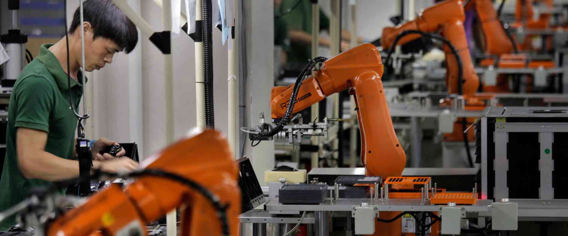
The car manufacturing industry has been utilizing industrial bots for over fifty years. The first robot to be in usage in this industry was known as UNIMATE, and it was adopted by the company General Motors back in the 1960s. However, after seeing how effective the robot was in producing high-quality products at lower costs, other automotive companies started to join the venture. Over time the number of bots utilized in the car building industry has massively grown. Moreover, the technology has not been left behind, too, with more flexible, low-cost collaborative systems replacing and supplementing the inflexible and cumbersome traditional robots.
Utilizing robots allows automotive components and car makers to reduce production time and cost while at the same time producing high-quality products. What’s more, robots are good for material handling and to undertake tasks that could cause harm to human beings leaving humans to do other tasks that could help them scale up the company’s ladder.
The invention of cobots or collaborative robots has brought new possibilities to the Car manufacturing industry. That is because you can deploy this robot to work side by side with human employees, optimizing the car assembly line process. Moreover, cobots allow car manufacturers to free human employees from dangerous, dirty, dull, and monotonous tasks, and they can also work at a high speed 24/7 without needing any rest. What’s more, by equipping this bots with a laser and camera array, they can be able to perform more tasks autonomously. However, these examples are just the tip of the iceberg regarding how robots have transformed the automotive industry.
Many industries benefit from the automation that comes with industrial robots, and the automotive industry stands at the top of the list. Since General Motors adopted the very first industrial robot in the car production process, countless other companies and warehouses also began to utilize the technology.
Now robots are applicable in many different industries, including the pharmaceutical industry, the medical industry, general manufacturing and the agricultural industry.
Universal bots are versatile, flexible and programmable to undertake countless tasks in varying environments. They reduce labor costs while simultaneously producing increased quality products at a fast rate.
When it comes to utilizing robots, the only limitation is safety compliance, the payload, and your imagination.
What does an Industrial Robot do?
Industrial bots utilized in the automotive manufacturing sector can handle many tasks that include inspecting finished products, pick and place tasks, packaging, palletizing, et cetera. Robots are specially designed to undertake highly monotonous tasks that could cause physical and psychological stress to human beings. Moreover, some industrial machines undertake strenuous physical tasks that could otherwise be challenging to humans.
Robot manufacturers can equip machines with artificial intelligence, machine vision systems and force sensing technology to help them respond to varying situations. With this system in place, manufacturers can gain real-time feedback from the robot regarding the manufacturing process.
The most common problems faced by car manufacturers include:
Slow production time
Injuries occurring during the production process
Producing low-quality products
However, we can solve all these issues using a robot.
For instance, Ford uses the UR10 robot Ford to fill car engines with oil, grease camshafts, and undertake quality inspections. Using this robot, Ford has been able to produce more cars in a short period. What’s more, employees in this company have been relieved from highly repetitive tasks.
Machines can undertake most physical tasks involved in the car production process. Moreover, they are also essential in carrying out decision-making tasks, for example, undertaking fail/pass quality inspections to ensure that the goods produced are of high quality.
Ways that Automotive Manufacturers utilize Robots in the Car Production Process
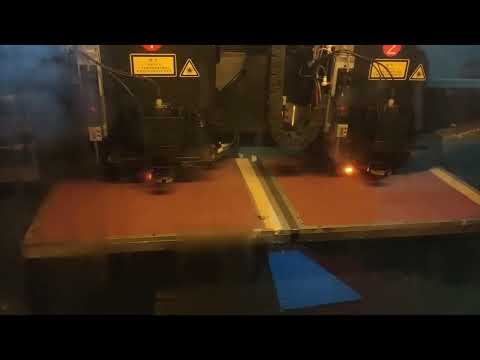
Robots have six primary applications in the automotive industry. These applications are undertaking quality inspection, material polishing and removal, machine tending, welding, painting, and assembly.
Before the invention of cobots, car manufacturers needed different robots to undertake each of the tasks mentioned above. However, now manufacturers only need one cobot to undertake all these tasks.
Automotive Assembly
Cobots undertake crucial tasks in the car manufacturing process, which include assembling the actual vehicles. Cobots can tackle monotonous tasks such as windshield installation and door handles installation with ease, relieving human workers from these tasks to help them focus on higher-value tasks.
Large industrial Robots that bear a higher payload, for example, the UR16 robot that has a payload of 35.3lb or 16kgs, can handle bulkier items, such as engine hoods, hatches, and wheels. On the other hand, the smaller robots known as UR5 cobot are lightweight and flexible and they are hence utilized by other companies to assemble car seats. The UR5 cobot bears a small footprint; this enables it to function well in tight spaces spaces where it can perform tasks such as:
– Assembling car seats
– Assembling rest frames
The UR5 can complete 8,500 screw driving actions in one day hence highly optimizing the production process of vehicles.
Painting bots have become pretty popular in the automotive manufacturing industry. That is because this robot offers impeccable performance round the clock and its painting performance is pretty consistent. Furthermore, since the paint utilized in the automotive industry is pretty toxic to humans, it poses a great issue that is solved using robots.
Challenging tasks, for example, applying even coats of paint on large car surfaces, are best undertaken by robots due to their precise work and consistency.
The performance and precision offered by industrial robots utilized to undertake painting tasks lowers production costs immensely. That is because these robots waste less paint, and they also eliminate human errors that cost a lot of money to fix.
Welding
Welding is a time-consuming, dangerous and monotonous task that industrial robots can perform better. Robots can tackle spot welding, plasma, ultrasonic, MIG, laser, TIG, and Arc welding with a lot of ease. What’s more, these robots can also undertake brazing and soldering.
UR and fanuc robots are pretty popular bots to undertake car welding tasks. These robots are pretty affordable and flexible. You will mostly find them in small car manufacturing companies.
Machine Tending
Machine tending is a task that is dull, dirty, and repetitive. Hence, the task is ideally good for robots as they perform repetitive tasks well. Recent research has shown that most automotive companies have now adopted machine tending robots in their automotive manufacturing process.
Bajaj auto motors, an automotive company located in India, heavily utilizes cobots in their car production process. The company was actually the first company in India to utilize cobots in its production process. Since then, the company has deployed over a hundred cobots and robotic arms which have helped optimize its assembly lines. Their cobots tackle challenging and repetitive tasks like machine tending.
Bajaj automotive company now seeks to improve their standard two-wheeler cars and boost their production speed with the help of cobots and robotic arms.
Polishing automotive parts and material removal are two tasks processes that are pretty crucial in the car production process. These processes involve cleaning up automotive parts along the way via trimming flash metal. They also involve polishing up molds for smoother finishes.
However, this task, just like multiple other tasks in the Car manufacturing industry, tends to be highly monotonous and sometimes even dangerous. Thus, collaborative robots are better placed to execute them.
Material removal tasks typically include Routing, Drilling, Sanding, Milling, Deburring and Grinding.
Robotiq, a robot-making company, has designed a series of finishing kits utilized by different automotive factories to optimize their production process. These finishing kits undertake highly repetitive tasks, such as sanding, surface finishing, and external tools finishing excellently.
The finishing kit includes Copilot software, a software specially designed by the company to help manufacturers program their robots to undertake finishing tasks. The software is user-friendly, and users can easily utilize it to program their bots regardless of their robotics expertise.
UR and fanuc robots, on the other hand, are designed to work in a flexible manner alongside human workers. Hence, they are in heavy usage in the car production process to undertake polishing and material removal tasks. Moreover, since these robots are tiny, they become applicable in small spaces.
Quality Control Bots
Quality inspection brings out the difference between a successful production and a labor-intensive, expensive failure. Since this process is pretty crucial in the car production process, most manufacturers opt to utilize cobots to minimize human errors and optimize the process.
UR bots come with a variety of software and hardware designed to help manufacturers automate the quality inspection process. These robots can perform tasks such as Metrology and Optical inspection.
Different companies worldwide utilize these robots for machine tending and quality inspection. The use of these robots helps reduce customer rejections while at the same time boosting the production process immensely. Most companies that opt to utilize bots in their assembly lines report zero defects encountered during their production process and even an increase in terms of production.
Pros of Robotic Applications in the Automotive Industry
Boosting Production Quality
Robots utilized in the automotive industry dramatically boost the quality of a product. That is because these bots perform multiple monotonous tasks with great precision. Moreover, these bots maintain consistency throughout the production process, ensuring high-quality products each time.
Increase throughput
Bots utilized in the automotive industry boost car production since they can work 24/7 without needing a break. Moreover, these robots maintain their precision throughout, helping manufacturers achieve throughputs that are hard to attain when working with human workers alone. Companies working with industrial robots report an increase in production almost instantly.
Boosting workplace safety
Robots utilized in the automotive industry boost workplace safety immensely. That is because they are useful in handling tasks that could cause harm to humans, for example, painting cars. They also handle highly monotonous tasks that leave humans to handle other tasks, for example generating new ideas to help the world.
Savings
Industrial robots in the automotive sector do not require a salary at the end of the month or insurance and healthcare, even though they can work 24/7. What’s more, robots boost the product quality of vehicles produced, which in turn leads to customer satisfaction. Manufacturers utilize this advantage to maintain customers, reduce costs and stay in business.
Reduced Injuries
Automotive companies utilize robots to undertake tedious, dirty, and risky tasks. In doing so, these companies experience fewer injury cases which in turn saves them money in terms of sick time and downtime.
Cons of Robotic Applications in the Automotive Industry
Initial Investment
Even though large industrial robots help car manufacturers save a lot of money over time via cutting labor costs and boosting production, they cost a lot of money to purchase. Therefore, most small-scale companies avoid purchasing them as it might mess with their budget.
If you are looking to purchase an industrial robot, be sure to include the bots purchase on the company’s budget. Doing so will help you make appropriate decisions about incorporating bots in your company.
No Result Guaranteed
Just purchasing a robot and incorporating it into your company does not guarantee that your production rate will automatically skyrocket. Therefore, before purchasing a robot to incorporate into your automotive company, devise a plan first. The plan will help you know the right bots to purchase to optimize your production process. Failure to have a plan prior to purchasing your robot could have a negative effect on you automotive company.
Need for Expertise
Industrial robots require a lot of expertise. Therefore, after purchasing an industrial robot, manufacturers then need to train their employees to utilize the bots effectively. Training takes time and requires the utilization of resources. Some car manufacturing plants even opt to bring in new employees who have experience in dealing with industrial robots. In doing so, they increase the number of employees waiting for a pay cheque at the end of the month.
Maintenance
Industrial robots must undergo maintenance every once to maximize efficiency. Besides, as new technology keeps on emerging every single day, sometimes these bots should undergo upgrades for manufacturers to cope with the market competition. All this action require the utilization of resources, and time.
Conclusion
Robots have countless applications in the automotive world. When utilized properly, they increase the quality of goods produced while at the same time reducing production time and cost. What’s more, robots help automotive manufacturers reduce workplace injuries by utilizing robots to tackle dangerous tasks.
Cobots or collaborative robots are pretty popular in the automotive industry due to their adaptability and flexibility. We can utilize collaborative bots on the factory floor, close to your employees. Moreover, these bots can fit in tiny spaces since they are pretty flexible and small. With these robots, car manufacturers have been able to optimize the production of their vehicles immensely hence transforming the automotive supply chain.
With the increasing adoption of IoT (internet of things), the connected devices have been able to penetrate all aspects of our lives. These include our home automation, health and fitness,logistics, automotive, industrial IoT, and smart cities.
Therefore, it is logical to imagine that IoT, automation, and connected devices would be applicable to agriculture. We also hope that it improves almost every aspect of it tremendously.
In the past decades, farming has experienced some technological transformations, thereby becoming more technology-driven and industrialized. By making use of different smart agriculture gadgets, our farmers have been able to gain better control of the entire process involved in the raising of livestock as well as growing crops. This makes it much more predictable. It also improves its efficiency.
All these, coupled with the rising consumer demand for all agriculture products, has led to an increase in proliferation of the smart farming technologies globally.
Here, we will explain the use cases of IoT in agriculture, as well as consider their benefits. Therefore, if you wish to invest in smart planning, or you wish to build an agricultural IOT solution, please read on.
We can talk about modern agriculture in many different ways. For instance, AgriTech deals with applying technology to agriculture generally.
On the other hand, smart agriculture is majorly used in denoting the agricultural application of the IoT solutions. Now, what does smart agriculture making use of IoT mean? When you use IoT sensors and IoT solutions for the collection of machine and environmental metrics, the farmers will be able to make the right and informed decisions. Also, they will be able to improve all areas of their work, including crop farming and livestock.
For example, when you use smart agriculture sensors in monitoring the crop’s state, farmers will be able to define the amount of fertilizers and pesticides they must use in reaching optimal efficiency. This also applies to the definition of smart farming.
Though smart agriculture IoT and industrial IoT generally are not as famous as the consumer connected devices, the market still remains very dynamic. Also, there is a constantly growing adoption of the IoT solutions in agriculture.
COVID-19 has impacted IOT positively in the market share of agriculture. Few qualified workers and supply chain disruption has caused the CAGR to about 9.9%. By 2025, the global market size of this agriculture should triple to reach $15.3 billion, in contrast to its slightly more than $5 billion in 2016.
IoT and Technologies have the ability to transform our agriculture in different aspects. There are five main ways by which IoT will be able to improve agriculture.
Tons of data which is collected by the smart agriculture sensors. These include soil quality, weather conditions, cattle’s health, crop health, and progress of crop’s growth. This data is useful in tracking how your business is performing, equipment efficiency, staff performance, etc.
More control over internal processes leading to lower risks in global agricultural production
Having the capability to foresee your production’s output lets you plan to have a much better product distribution.
Waste reduction and cost management due to better control over production
When you are able to see anomalies in your livestock health, crop health, or crop growth, then it becomes possible to mitigate any risks involved in losing any yield.
Better business efficiency via process automation
When you use smart devices, then it becomes possible to automate many processes all through the production cycle. For example, pest control, fertilizing, or irrigation.
Enhanced volumes and product quality
Achieving much better control on the process of crop production, as well as maintain much higher standards of the crop quality as well as growth capacity via automation. Due to this, these factors will eventually result in higher revenue.
Now, we have learnt about how IoT can be beneficial to agriculture. Now, let’s consider ways in which these benefits will be applicable in real life.
What are the Use Cases or Applications of IoT in Agriculture?
IoT sensors meant for agriculture come in different types. This also includes IoT applications in all agriculture generally.
Monitor Climate Conditions
The most famous gadgets for smart agriculture system include weather stations, which combine different smart farming sensors. Their location is usually across the fields where they collect different data from our environment and then send it into the cloud.
Furthermore, the measurements provided are useful in mapping these climate conditions, choosing appropriate crops, as well as taking the necessary measures in improving their capacity, for example in precision farming.
Greenhouse Automation
Farmers usually make use of manual intervention for controlling any greenhouse environment. Using IoT sensors makes it possible to be able to get the best real-time information regarding greenhouse conditions like humidity, soil conditions, temperature, and lighting.
Also, adding to the sourcing of environmental data, the weather stations have the ability to adjust conditions automatically to help in matching the necessary parameters. Greenhouse automation systems usually make use of similar principles.
Growlink and Farmapp are IoT agriculture products which offer some capabilities. Also, GreenIQ is an interesting product which makes use of smart agriculture sensors. Also, it is a well-known smart sprinklers controller, which allows the management of lighting and irrigation systems remotely.
Crop Management
Another type of the IoT product in agriculture, as well as a different precision farming element are the crop management devices. Like the weather stations, you have to place them in a specific field to help in collecting data that is crop framing specific. These include precipitation, temperature, general crop health, and potential of leaf water.
Therefore, you will be able to monitor the crop growth, as well as anomalies that prevent infestations or diseases effectively,which could bring harm to your yield.
Cattle management and monitoring
Similar to crop monitoring, some IoT agriculture sensors exist, which could be attached onto animals present on a specific farm in monitoring their log and health performance. With livestock monitoring and livestock tracking, you will be able to get reliable data on physical location, well-being, and stock health.
For instance, these sensors will be able to locate the sick animals, which will help farmers to separate them from the others to prevent contamination. Making use of drones from the real-time tracking will also assist farmers i9n reducing staffing expenses. Its function is similar to the IoT devices for petcare.
This is also called precision agriculture. It refers to efficiency as well as producing data-driven decisions that are accurate. Furthermore, it is included among the most effective and widely used applications or use case of the IoT in agriculture.
When you make use of IoT sensors, farmers will be able to collect different metrics on every aspect of the field’s ecosystem and microclimate. These include humidity, soil condition, temperature, lighting, pest infections, Co2 levels, and humidity. Also, the data allows farmers to get an estimate of the right amounts of pesticides, fertilizers, and water, which is useful for their crops, raise healthier and better crops, as well as reduce the necessary expenses.
For example, CropX helps in building IoT soil sensors, which measures the soil temperature, moisture, as well as electric conductivity. This allows the farmers to consider each of the unique needs of crops.
Agricultural drones
One very promising and well-known AgriTech advancements is the utilization of agricultural drones in our smart farming. This is also called unmanned aerial vehicles (UAVs). These drones are more equipped than the satellites and airplanes in collecting agricultural data.
Asides from their surveillance capabilities, these drones have the ability to carry out different tasks that required the use of human labor previously. These include fighting infections and pests, crop monitoring, agricultural spraying, planting crops, locating shrinking agricultural lands, etc.
Predictive Analytics
Predictive data analytics and precision agriculture work together. While the smart sensor and IoT technology can serve as a goldmine for the real time data, using data analytics assists farmers in making some sense from it, as well as having some important predictions. These include time for crop harvesting, risks of infestations and diseases, yield volume, and more. Also, the tools for data analytics help to ensure farming. This depends inherently on the weather conditions, which are more predictable and manageable.
Management Systems
You can represent a very complex approach to the IoT products used in agriculture by the management systems of farm productivity. Usually, they include some agriculture IoT devices and IoT sensors, which are installed on these premises, coupled with a strong dashboard having analytical capabilities, as well as in-built reporting and accounting features.
Furthermore, this provides capabilities of farm monitoring that allows users to be able to streamline the majority of their business operations.
Asides from the listed use cases of IoT in agriculture, there are some important opportunities, which includes storage management, vehicle tracking, automation, logistics, etc.
What you should Consider Before You Develop a Smart Farming Solution
iot smart farming
Now you can see that the applications of IoT in agriculture are numerous. There are lots of ways through which smart devices will be able to assist you in increasing the revenue and performance of your farm. However, developing agriculture IoT apps is a difficult task.
There are some challenges you must take note of if you wish to get involved in smart farming applying IoT in agriculture.
The brain
The data analytics has to be the center of any smart agriculture solution. This collected data will offer little assistance if you fail to make proper sense of it. Therefore, there is a need to have strong data analytics capabilities, as well as apply some machine learning and predictive algorithms to help in obtaining actionable insights that are based on this collected data.
The hardware
In order to create an effective IoT solution for our agriculture, there is a need to go for device sensors. You can also create a custom sensor. Whatever choice you make depends on the information you wish to collect, as well as your solution’s purpose generally. Whatever the case is, your sensor’s quality is important to your product’s success. It depends on the accuracy of any data collected, as well as its reliability.
The mobility
The applications of smart farming must be tailored to be used in this field. As a farm manager or business owner, you should have access to the information remotely or on site through a desktop computer or smartphone.
In addition, each of the connected device has to be autonomous, as well as possess the wireless range necessary to be able to communicate with the other devices, as well as send data onto the main and central server.
Connectivity
There is a need for data transmission between the many different agricultural facilities. This is a challenge for smart farming adoption. Today, the IoT devices make use of different connection protocols, though efforts required for developing the unified standards are presently underway. Furthermore, the advent of technologies and 5G space-based internet hopefully, should find a solution to the problem.
There is a need to have a strong internal infrastructure to make sure that your application for smart farming performs properly as well as ensure it handles the data load properly.
Also, the internal systems must be secure. When you don’t secure the system properly, it once increases the possibility of anyone breaking into it, to steal your data, as well as take control of the autonomous tractors.
Maintenance
Maintaining your hardware could be a major challenge which is very important for the IoT products used in agriculture. This is because the sensors are useful in this field and can get damaged easily. Therefore, ensure that the hardware is easily maintained and is durable. Otherwise, you will end up replacing these sensors too often.
Data Security
IoT technology and precision agriculture implied working with different large data sets. This increases possible security loopholes, which perpetrators could use for hacking attacks and data thefts. For example, many farms make use of drone to transmit data to the farm machinery. The machinery helps in connecting to the web. However, it has very little to no security protection like user passwords.
Some basic security recommendations for IoT in agriculture include the use of encryption methods in protecting sensitive data, monitoring of data traffic, storage of data in blockchain to keep its integrity.
Conclusion
We have explained in detail the applications and uses of IoT in agriculture. We hope more advancements in agriculture result from the use of IoT technology.
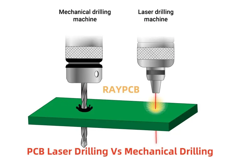
Laser drilling enables ultra-precise hole formation in PCBs, creating critical interlayer connections that power today’s advanced electronics. This technology is essential for manufacturing high-density interconnect (HDI) boards found in modern slim devices like smartphones and wearables. Unlike mechanical drilling, laser systems achieve unmatched accuracy—even at microscopic scales—ensuring reliability in increasingly miniaturized designs.
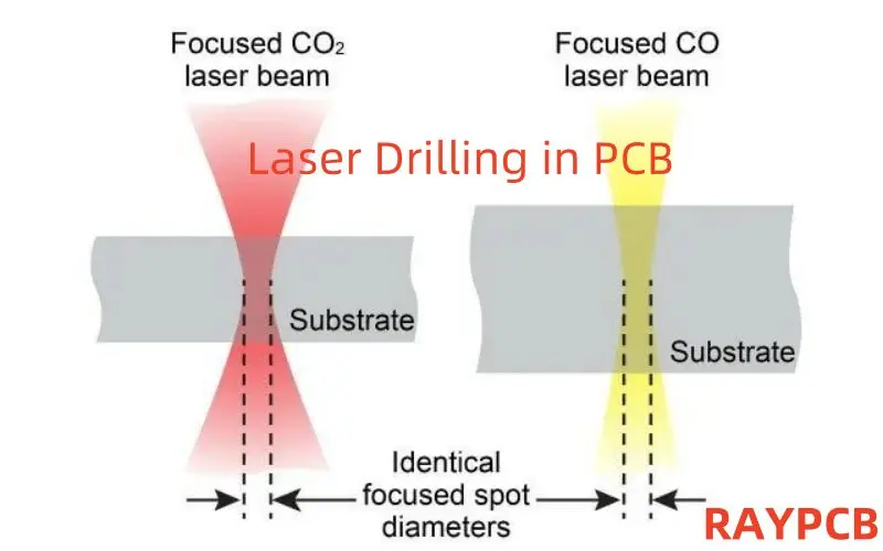
The process harnesses concentrated laser energy (from CO₂ or UV sources) to vaporize material with pinpoint precision. As an acronym for Light Amplification by Stimulated Emission of Radiation, a laser’s coherent beam eliminates physical contact, avoiding mechanical stress and enabling cleaner, smaller holes than traditional drill bits can produce.
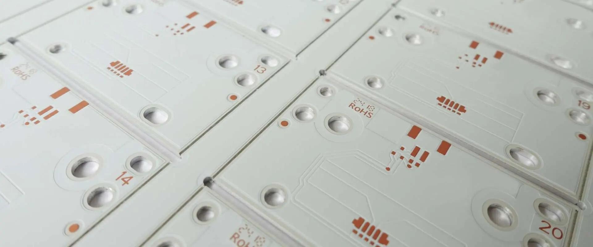
What is Circuit Board Drilling?
Circuit board drilling is a fundamental process in PCB manufacturing that involves creating holes in the board substrate. These holes serve various purposes, including:
Mounting components
Creating electrical connections between layers
Facilitating the flow of signals and power
Traditionally, mechanical drilling has been the go-to method for creating these holes. However, as PCB designs become more complex and miniaturized, laser drilling has gained prominence, especially for creating smaller, more precise holes.
Why is Laser Drilling Required for PCB?
Laser drilling has become increasingly essential in PCB manufacturing due to several factors:
1. Miniaturization
As electronic devices become smaller and more powerful, PCBs must accommodate more components in less space. Laser drilling allows for the creation of extremely small holes, enabling higher component density.
2. High-Density Interconnect (HDI) Boards
HDI boards require a large number of small, precise holes to connect multiple layers. Laser drilling is ideal for creating these microvias efficiently.
3. Precision
Laser drilling offers unparalleled accuracy in hole placement and size, which is crucial for advanced PCB designs.
4. Material Compatibility
Lasers can drill through a wide range of PCB materials, including those that are difficult to process with mechanical drills.
5. Non-Contact Process
Unlike mechanical drilling, laser drilling is a non-contact process, reducing the risk of damage to delicate board structures.
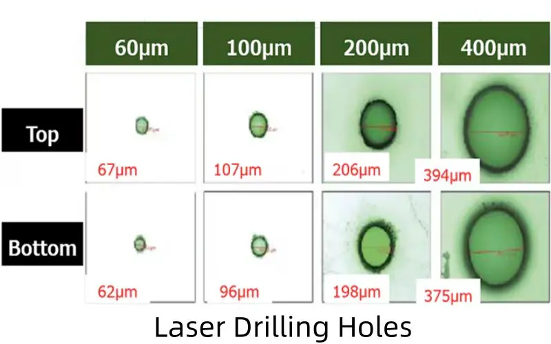
One of the most significant advantages of laser drilling is its ability to create extremely small holes. The size of holes that can be laser-drilled depends on several factors, including:
The type of laser used
The material being drilled
The thickness of the PCB
Typically, laser drilling can create holes as small as 25 microns (0.001 inches) in diameter. Some advanced systems can even produce holes as small as 10 microns. This capability is crucial for creating microvias in HDI boards and enabling the production of increasingly compact electronic devices.
Advantages of Laser Drilling
Laser drilling offers numerous advantages over traditional mechanical drilling methods:
1. Precision and Accuracy
Lasers can create holes with extremely tight tolerances, ensuring consistent size and placement.
2. High-Speed Processing
Laser drilling can be performed at very high speeds, increasing productivity in PCB manufacturing.
3. Flexibility
Laser systems can be quickly reprogrammed to accommodate different hole patterns without changing physical tooling.
4. Reduced Wear and Tear
As a non-contact process, laser drilling eliminates the need for physical drill bits, reducing maintenance and replacement costs.
5. Clean Process
Laser drilling produces less debris and doesn’t require cutting fluids, resulting in a cleaner manufacturing environment.
6. Ability to Drill at Angles
Some laser systems can drill holes at angles, which is difficult or impossible with mechanical drilling.
7. Suitable for Delicate Materials
Laser drilling can process thin and fragile materials without causing damage or delamination.
Different Methods of Laser Drilling
Laser drilling techniques have evolved to meet various manufacturing needs. Here are the primary methods used in PCB production:
1. Single-pulse/Shot Laser Drilling
This method uses a single, high-energy laser pulse to create a hole.
Advantages:
Very fast process
Suitable for thin materials
Limitations:
Limited hole depth
May not be suitable for all materials
2. Percussion Laser Drilling
Percussion drilling uses multiple laser pulses to gradually create a hole.
Advantages:
Can create deeper holes than single-pulse drilling
Offers better control over hole shape
Limitations:
Slower than single-pulse drilling
May cause more heat-affected zones around the hole
3. Trepanning
Trepanning involves using the laser to cut around the circumference of the desired hole.
Advantages:
Can create larger holes with very smooth walls
Allows for precise control of hole diameter
Limitations:
Slower than other methods for small holes
May not be suitable for very small hole sizes
4. Helical Laser Drilling
This method uses a rotating laser beam to create holes in a spiral pattern.
Advantages:
Can create deep holes with high aspect ratios
Produces very smooth hole walls
Limitations:
Requires specialized equipment
May be slower for certain applications
Which Lasers are Suitable for Drilling Micro Holes?
Several types of lasers are used for drilling micro holes in PCBs, each with its own strengths:
1. Excimer Lasers
Ideal for creating very small, precise holes
Commonly used for microvias in HDI boards
2. Solid-State Lasers
Include Nd:YAG and fiber lasers
Offer good precision and are suitable for a range of materials
3. CO2 Lasers
Widely used for drilling in organic PCB materials
Cost-effective for many applications
4. Ultrafast Lasers
Include femtosecond and picosecond lasers
Provide extremely high precision with minimal heat-affected zones
The choice of laser depends on factors such as the PCB material, required hole size, and production volume.
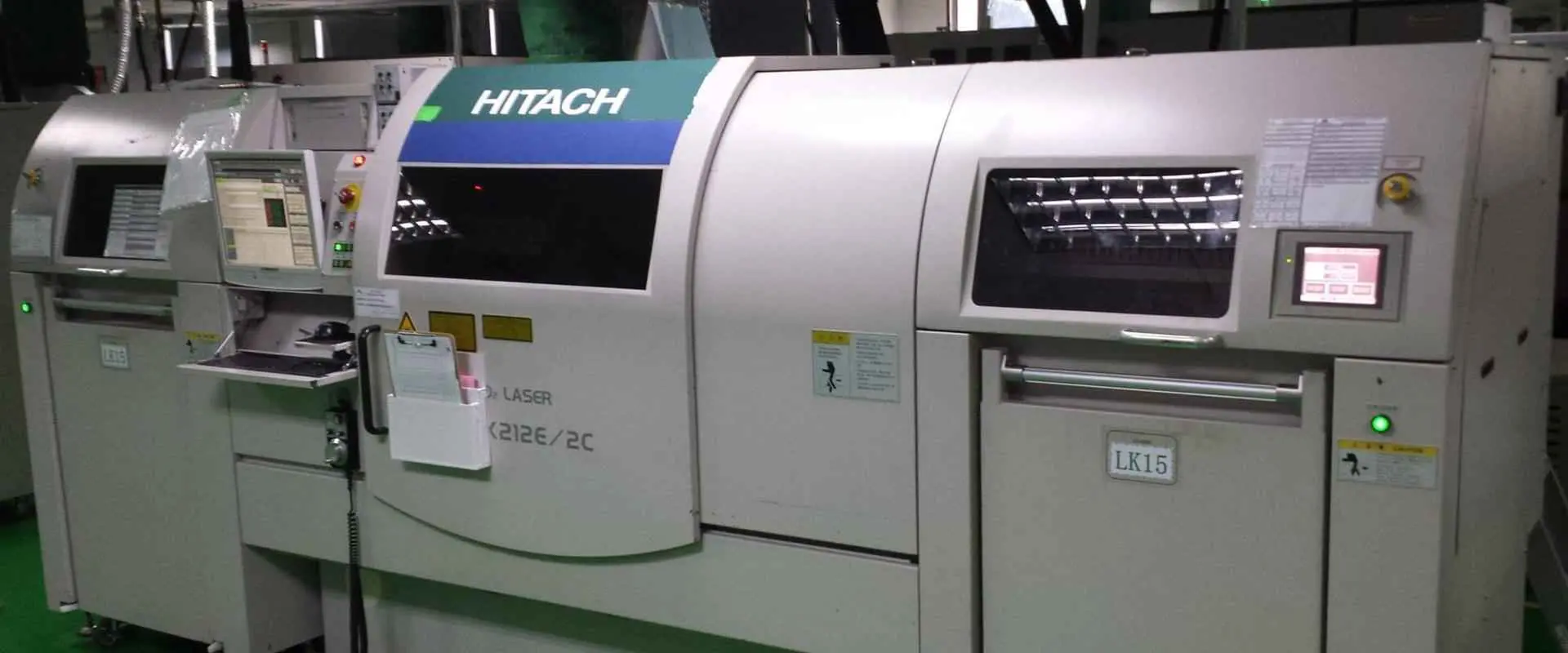
Types of Laser Drilling Machines
Laser drilling machines come in various configurations, each suited to different PCB manufacturing needs:
1. CO2 Lasers
CO2 lasers are widely used in PCB manufacturing due to their versatility and cost-effectiveness.
Limited in drilling very small holes (typically >75 microns)
Not suitable for some metal-based materials
2. Nd:YAG Lasers
Nd:YAG (Neodymium-doped Yttrium Aluminum Garnet) lasers offer high precision for micro-drilling applications.
Advantages:
Can drill very small holes (<50 microns)
Suitable for a wide range of materials, including metals
High peak power for efficient drilling
Limitations:
Higher initial cost compared to CO2 lasers
May require more maintenance
3. Combination of Nd:YAG and CO2 Laser Processes
Some advanced PCB manufacturing systems combine both Nd:YAG and CO2 lasers to leverage the strengths of each technology.
Advantages:
Versatility to handle a wide range of materials and hole sizes
Optimized processing for different PCB layers
Limitations:
Higher system complexity and cost
Requires expertise to manage multiple laser technologies
PCB Laser Drilling vs Mechanical Drilling
While both laser and mechanical drilling have their place in PCB manufacturing, it’s important to understand their differences:
Laser Drilling
Advantages:
Can create extremely small holes (down to 10-25 microns)
Non-contact process, reducing wear and tear
High precision and repeatability
Suitable for delicate and thin materials
Limitations:
Higher initial equipment cost
Limited in creating larger holes efficiently
May have issues with certain materials (e.g., some metals)
Mechanical Drilling
Advantages:
Cost-effective for larger hole sizes
Can drill through multiple board layers efficiently
Suitable for a wide range of hole sizes
Limitations:
Limited in creating very small holes (<75 microns typically)
Tool wear can affect precision over time
May cause burrs or rough edges requiring post-processing
The choice between laser and mechanical drilling often depends on the specific requirements of the PCB design, production volume, and available budget.
Facts about PCB Laser Drilling Cost
While laser drilling offers many advantages, cost is an important consideration for manufacturers. Here are some key facts about PCB laser drilling costs:
1. Initial Investment
Laser drilling equipment requires a significant upfront investment, often higher than mechanical drilling systems.
2. Operating Costs
Lower consumable costs (no drill bits to replace)
Potentially higher energy consumption
Specialized maintenance may be required
3. Throughput Considerations
Laser drilling can be faster for small holes, potentially reducing per-unit costs
For larger holes, mechanical drilling may be more cost-effective
4. Material Costs
Some materials optimized for laser drilling may be more expensive than standard PCB materials.
5. Long-Term Cost Benefits
Reduced need for rework due to higher precision
Ability to produce more complex boards, potentially increasing product value
6. Scalability
Laser drilling systems can often be scaled more easily to meet increased production demands.
While the initial cost of laser drilling may be higher, it can offer long-term cost benefits, especially for high-volume production of complex PCBs.
Laser-Drilled Microvia-in-Pad Technology in Your HDI PCB
Laser-drilled microvia-in-pad technology is a crucial advancement in High-Density Interconnect (HDI) PCB design. This technique involves creating small, laser-drilled vias directly in the pad of a component, offering several benefits:
1. Increased Routing Density
By placing vias directly in component pads, designers can achieve higher routing density and more efficient use of board space.
2. Improved Signal Integrity
Shorter connection paths reduce signal degradation and improve overall signal integrity.
3. Enhanced Thermal Performance
Microvia-in-pad can improve thermal dissipation, crucial for high-power components.
4. Reduced Board Size
This technology allows for more compact PCB designs, essential for miniaturized electronic devices.
5. Support for Advanced Packaging
Microvia-in-pad is crucial for supporting advanced component packages like Ball Grid Arrays (BGAs) with fine pitches.
Implementation Considerations:
Requires precise control of laser drilling parameters
May need specialized PCB materials for optimal performance
Demands careful attention to plating and filling processes
As electronic devices continue to shrink while increasing in functionality, microvia-in-pad technology enabled by laser drilling will play an increasingly important role in PCB design and manufacturing.
Conclusion
Laser drilling has revolutionized PCB manufacturing, enabling the production of increasingly complex and miniaturized electronic devices. Its ability to create precise, small-diameter holes is crucial for high-density interconnect boards and advanced packaging technologies.
While laser drilling offers numerous advantages in terms of precision, flexibility, and ability to work with delicate materials, it’s important to consider factors such as cost, specific application requirements, and material compatibility when choosing between laser and mechanical drilling methods.
As technology continues to advance, we can expect further innovations in laser drilling techniques and equipment, potentially opening up new possibilities in PCB design and electronics manufacturing. Manufacturers and designers who stay abreast of these developments will be well-positioned to create cutting-edge electronic products that meet the ever-increasing demands of the modern world.
Whether you’re a PCB designer, a manufacturer, or simply someone interested in the intricacies of electronics production, understanding laser drilling technology is key to appreciating the complexity and precision that goes into every electronic device we use in our daily lives.
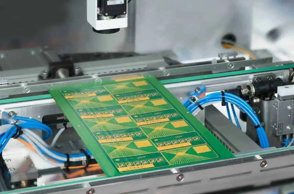
PCBs (Printed Circuit Boards) are becoming pretty popular in the 21st century. With the demand for smaller, powerful gadgets increasing, manufacturers are turning to PCB to make this devices a reality. Printed Circuit Boards connect each component found inside an electronic gadget, helping it function accordingly. Due to their compactness and versatility, PCBs have become pretty popular in light production companies, electronic companies and so on.
However, even though PCBs are tiny, they are pretty tricky to manufacture as you need to remember tricky factors such as impedance control and copper weight. Therefore, most people turn to PCB manufacturing companies to build their PCBs. But what Printed circuit board printing services can you get out there? And what are the benefits of turning to PCB manufacturers to make your PCB?
PCBs are typically built using bare boards made out of copper. The PCB manufacturer then utilizes high-tech gadgets and other components such as Gerber files to curve the client’s design on the copper board to develop a Printed Circuit Board.
In case the PCB encompass multiple layers, the PCB Manufacturer must then line up the layers and then bind them to attain a secure fit.
The process takes up a lot of time, and PCB manufacturers have to be extra careful to avoid messing up the design handed over to them by the customer. What’s more, it is possible to break down the entire process into multiple stages, each of which is pretty crucial to attaining the end product.
Printed Circuit Board Services
What the Manufacturer needs from you
Gerber Files
Before providing any PCB services, the PCB manufacturer has to request for a Gerber file. These open ASCII files contain details on every Physical PCB layer on your board design be it a hobby design or a complex design. PCB objects, for example, silkscreen images, solder mask, vias, and copper traces, are all well represented using a draw code or a flash. They are then defined using vector coordinates.
After undertaking a file check, manufacturers then utilize these crucial files to translate your PCB design into an actual PCB at an affordable price.
Generating a Gerber file
Generating Gerber files is pretty easy because the only tool you will require will be a PCB designing software. However, the process of developing the actual correct design tends to vary depending on the software you will utilize. What’s more, these files do not have to bear unique names. However, they all have a standard extension, for example, .gbr or .gb.
Once you have made your Gerber file, you can then advance to the next stage.
PCB Fabrication Services
If you are having trouble producing your PCB from scratch, you can easily find a manufacturer online to generate a custom PCB for you. Of course PCB fabrication is not free and you will have to pay some amount of money, but the outcome is worth every penny.
In most cases, the PCB manufacturer will ask you for the following parameters before processing your PCB order:
The Parameters
– Board type – The Manufacturer will need to learn details on the board type that you want
– Size – Here, you will have to provide the PCB’s maximum length and width. Using this information, the PCB manufacturer will easily figure out the maximum size of your PCB
– Number of PCB being produced – here, specify whether you want a single board or if you want your PCBs produced in batch production form.
– Layers – You specify the number of layers the PCB will have. For example, if you want your PCB to bear one layer, then you can simply request for a one layer PCB.
– Base Material – Here, specify the type of base material that you want your Manufacturer to utilize. For example, you can opt to work with aluminum or rogers. Some companies will also ask whether you want a metal core or a plastic core.
– Board Thickness – Specify the parameters that describe the printed circuit board thickness. Using this information the PCB manufacturing company will figure out the right copper weight to use.
– Min spacing/track – Here, you must clearly state the minimum track spacing. Using this information, the manufacturer can figure out the trace width to utilize.
– Min hole size – Specify the minimum hole size to help the Manufacturer during the drilling process.
– Solder mask – Here, provide details regarding the type of solder mask that you want to be utilized on your PCB
– Silkscreen – silkscreen comes in two varieties, white and black. You can opt for either of the two. Or you can choose to utilize your Printed circuit board without a silkscreen.
– Surface finish – choose the surface finish that you want your Manufacturer to utilize on your PCB.
You can also opt for a lead or a lead free PCB. Doing so helps your PCB manufacturer known the type of solder paste to use on your circuit boards and the lead time needed to produce your PCB.
A Gerber file should also accompany all these details to help the Manufacturer get your design right in the PCB fabrication process.
Using these details, a PCB manufacturing companies such as PCB partner can easily print out your PCB order using high-tech machines with remarkable precision. However, you should always double check on the Manufacturer’s experience before handing out the contract. Doing so will ensure that you get a high-quality finished product in return while avoiding hidden costs and scam companies. You can also contact the PCB manufacturing company via a message or through a phone call. Using this methods, you can easily discuss critical issues such as the price of developing your PCB and how long it will take to receive your board.
Exclusive Services
Some companies will offer exclusive services which feature special requirements meant to make more advanced circuits and more efficient PCBs. These exclusive solution, however, do not come at a low cost, therefore be keen when making such an order.
Other services offered for the Printing of Printed Circuit Boards
PCB Drilling
The PCB drilling process tends to be the most tiresome, time-consuming, and expensive phase of the PCB manufacturing process. That is because PCB manufacturers have to carry out this stage carefully to ensure that they develop a high-quality PCB.
The PCB holes can be generated via electrochemical etching or via punching, laser cutting, or drilling. However, most PCB manufacturers tend to favor a combination of electrochemical etching and chemical milling to carry out this process.
Solder mask PCB Assembly and Printing
After Printed Circuit Board Fabrication, the traces of copper left on the PCB are prone to corrosion and oxidation due to exposure to the environment. The best way to shield your PCB against these issues and boost its durability is by placing a protective layer on the PCB known as a solder mask layer.
A solder mask is pretty crucial in terms of helping boost the durability of a PCB. However, the solder masking process can be pretty tricky to carry out. But the good thing is that you can easily find a PCB manufacturer to carry out this process.
Types of Solder Mask Services Offered
There are several solder mask services offered in the PCB market today. These services include:
– Bottom and top side masks – These solder masks are utilized mainly by engineers to help them identify various openings on a Print Circuit Board.
– Epoxy liquid – If you are looking for an affordable solder mask, then this should be your first option. Epoxy is an excellent polymer, and it offers great protection to your PCB at a reasonable cost.
– Liquid photoimageable – LPI or photoimageable is a solder mask that is a mixture of two different liquids. The liquids used to make this solder mask are stored separately and are only mixed right before they are applied to the PCB to ensure longer shelf life.
– Dry film photoimageable – Dry film photoimageable is a solder mask that best suits high-density wiring Printed Circuit Boards. That is because these solder masks do not flood the prior put through-holes. It is hence pretty efficient.
Surface Finish
PCB Manufacturing with Immersion Gold-ENIG Surface Finish
In most cases, the solder mask utilized on a PCB tends to leave behind exposed copper areas on the PCB. These areas have to be plated using a suitable surface finish so as to lower the chances of oxidation. PCB manufacturers worldwide are now offering surface finish services to help clients cope with this issue easily.
Also under this category, some manufacturers are now offering copper plating service. These services help boost the thickness of a PCB making it more rigid and efficient.
Surface Treatment PCB Assembly Services
Printed Circuit Board surface treatment refers to the crucial process of creating a surface layer on a PCB artificially. The reason why this process is vital is that it helps to boost the electrical and soldering properties of a PCB.
Many surface treatment services exist. Here are some common surface treatment services that you can find:
Hot air Solder Leveling or HASL
HASL is a simple process whereby a PCB manufacturer coats your PCB using molten tin-lead solder. They then flatten the molten tin lead using heated compressed air to form a layer resistant to copper oxidation. Moreover, this layer is resistant to copper oxidation, making a PCB more efficient and durable.
During this process, the following parameters have to be mastered:
OSP or organic protective film works by spraying organic chemicals on a Printed Circuit Board to provide a protective layer. An OSP layer has to bear the following characteristics for it to work:
– It should be shock resistant
– It should have oxidation resistance properties
– And lastly, it should have moisture resistance properties
Immersion Silver
Typically silver bears stable chemical properties. Therefore, Printed Circuit Boards that have undergone the immersion silver process tend to have excellent electrical properties even when exposed to pollution, humidity, and heat.
Immersion tin
After inserting organic additive into a tin immersion solution, the layer of tin that comes out of this mixture tends to overcome common issues caused by tin and tin whisker migration. With these issues out of the way, the circuit board tends to have better solderability and thermal stability.
Conclusion
Printed Circuit Boards have become a primary component of the 21st century. Almost every gadget you come across now bears a PCB, be it a computer, a street light, or even a flashlight. But, even though these components are crucial, manufacturing them can be challenging for many people. However, with the emergence of multiple companies bearing skilled engineers willing to manufacture Printed Circuit Boards for various clients, this issue is starting to become extinct. Therefore, if you want to print a PCB or add new features to your PCB but do not have the equipment to do so, remember that you can easily find a manufacturer to help you out even though it won’t be for free.
Are you looking for a job in the digital IC design industry? Do you know how to find companies that design ICs in China? If you’re an engineer, designer, entrepreneur or investor in the semiconductor industry, this post will interest you.
What is digital IC design?
A proper digital IC design begins with a specification of the desired function. The specification can come from an outside source, or the manufacturer can provide it. Then the specification is translated into a Verilog or VHDL netlist, then verified against the specifications. Finally, there is synthesis of the netlist to produce a physical layout. Gate layouts are usually available from the IC manufacturer’s libraries.
Those working on the design process translate the specifications into digital blocks and logic circuits. The process is procedural, but many constraints associate with this type of IC. The design process is a combination of technological constraints and foundry processes. These factors result in several possible designs.
Creating a digital Integrated Circuit (IC) involves translating a set of determinations into computerized blocks assembled into basic circuits. The development of advanced IC plans, including the design of a foundry cycle, involves the advancement of frameworks and cycles. Creating a digital IC is not as simple as creating a conventional one; it requires extensive education and specialized training.
Digital designers can use libraries provided by IC manufacturers, which contain information on gate delay and layout.
Current Status of IC Industry in China
In February 2021, prediction aligned China’s IC industry to meet 70% of the domestic demand. Homegrown silicon was integral in meeting the demand, but in February, US sanctions began to bite. Meanwhile, China’s production remained below global standards and faced an increasing capacity gap.
In terms of volume, semiconductor demand in China was USD155 billion, with about 38% coming from non-Chinese companies. The largest demand came from four major Chinese smartphone companies and a non-China ICT company. Overall, China’s IC industry generated USD23.7 billion in local manufacturing, which was only 23.7 percent of the global demand. In contrast, China’s local IC manufactured industry produced only USD23.7 billion the previous year.
Vimicro Corporation
The Vimicro Corporation is a technology company founded in Beijing, China, in 1999. Its founders, who came from Silicon Valley, received support from the Ministry of Information Industry in establishing the company. Vimicro is dedicated to developing advanced mixed-signal multimedia chips and has several products currently available for domestic and international markets. Vimicro’s products target several fast-growing application fields.
Vimicro Corporation is a leading fabless chip company based in Beijing. Vimicro develops mixed signal multimedia chips, including video processors and networked video applications. It is the first Chinese chip design company with proprietary technology listed on Nasdaq. As one of the most influential and innovative chip companies in China, Vimicro has a strong market presence in the region and already incorporated into several Chinese companies.
Its patent portfolio spans over 2094 patents worldwide, belonging to 15 unique patent families. Of these, 687 are active and have received 73 citations. The company’s recent AI processor is for low power consumption and super-fast processing. It was also recently teamed up with the Ministry of Public Security to draft part of a national standard on video surveillance, which can help crack crimes. China has one of the world’s largest video surveillance networks and will be able to benefit from this development.
Its business
While a company’s performance does not necessarily reflect the future, many factors could affect its growth in China. These factors include the company’s ability to attract and retain employees. The company also faces several risks related to its business, including currency fluctuations. While investors should monitor the risks associated with investing in the company, these factors do not necessarily indicate that Vimicro is not likely to grow. While this situation is somewhat unlikely, management expects that its business in China will continue to grow in the coming years.
The Vimicro Corporation products target the rapidly growing markets of video surveillance, broadcast TV, gaming, and digital signage. With two decades of history, Vimicro is a company to watch in China.
Jingjia Micro’s latest GPU is called the JM7200. The new chip is a 28nm version of the company’s previous GPU, which was robust enough for military aircraft displays. It is compatible with OpenCL 2.0 and OpenGL 4.5 APIs. It will not compete directly with the best-selling AMD and NVIDIA GPUs, but it will be able to take on both companies in the data center and cloud computing segment.
Jingjia Micro, a military-civilian integrated company focusing on graphics processing, made the latest GPU. The company developed China’s first homegrown GPU, the JM5400, and is now promoting it outside the military sector. Its latest chip is about the same speed as the GeForce GTX 1080, so it is capable of boosting gaming performance.
Jingjia Micro’s upcoming GPU could match AMD’s Radeon RX 560 or GeForce GTX 1080
Jingjia Micro has been waiting for the right moment to release its first marketable GPU for years. The company recently dropped its first domestically produced GPU, the JM9231. The company’s upcoming GPU is comparable to the GeForce GTX 1080 or Radeon RX 560 in terms of performance and power consumption. Jingjia Micro’s upcoming GPU contains a TDP of only 150W, similar to GeForce GTX 1080 or Radeon RX 560.
Besides, the company’s upcoming GPU could match the prices of GeForce GTX 1080 and Radeon RX 560. Besides, the upcoming GPU from Jingjia Micro could match the price tag of AMD’s Radeon RX 560. Although Lao Huang’s claims may seem overly optimistic, it’s a good sign. The company is planning to launch two graphics cards. The entry-level JM9231 will be competitive with AMD Radeon RX 560 or GeForce GTX 1080. The JM9271 is more powerful and could even match GeForce GTX 1080 or GeForce GTX Vega 64.
Jingjia Micro’s non-public offering of stocks
The company plans to use the funds raised from the stock sale to invest in consumer electronics, high-performance graphics processor chips, and general-purpose chips. The fundraising effort aims to further strategic planning in IC design for the consumer electronics sector. Sino IC Capital Management will manage the China Integrated Circuit Industry Investment Fund. The raising of the funds will happen through the Hunan High-Tech Venture Capital Investment Group, a government-backed investment platform that aims to foster strategic emerging industries.
The Goke Microelectronics Company is a Chinese IC design firm. This company provides professional services and develops chips for satellite, digital cable, wireless communication, and DTMB. Its product line includes a H.265 HD video chip, modern solid storage controlling chip, Wi-Fi, and an NDS advanced security decoding chip.
Integrated circuit design enterprise
Founded in 2008, Goke Microelectronics Co., Ltd. is a leading provider of multimedia chip solutions in China. Its core technologies include intelligent 4K decoding chip, H.264/H.265 HD security chip, high-end solid-state memory master control chip, and Beidou navigation and positioning chip, which has independent intellectual property rights.
Government subsidies received
GOKE MICROELECTRONICS, a semiconductor manufacturer, received nearly $100 million in government subsidies in 2018 and another $24 million in 2017. These amounts are the total government subsidy amounts the firm received during the calendar year. You calculate the amount of subsidies received using the year-average exchange rate of the Chinese Yuan. GOKE may have also received other types of state aid.
Risk of being included in the Entity List
Currently, the Chinese company is part of the Entity List for Semiconductors, Chips, and Advanced Electronics. Its main product lines include microprocessors, flash memory, and integrated circuits for artificial intelligence and quantum computing. Goke has headquarters in Changsha, central Hunan province. One of its subsidiaries, New H3C, is an independent semiconductor, information technology, and financial company.
The primary focus of Giantec Semiconductor Corporation is providing integrated circuit products and services to customers worldwide. The company offers products for diverse industries including electronics, telecommunication, smart energy meters, medical and transportation. All its products meet or exceed the international standards and are marketed to customers worldwide.
A semiconductor company headquartered in Shanghai, Giantec Semiconductor is one of the largest suppliers of EEPROM chips. These chips are useful in storing configuration parameters in smart devices, personal computers, and other tools of the digital age. The company accounted for over 80% of its operating income in the first half of 2019.
The company is part of a larger industry and has an impressive customer base in Asia. Its automotive business has helped it establish a strong presence in China, a major EEPROM market. Its products include two-wire serial EEPROMs, application-specific ICs, and smart cards. It also manufactures signal chain-operation amplifiers, automotive parts, and VCN drivers.
Gross profit margin
Founded just a decade ago, the Shanghai-based semiconductor giant Giantec Semiconductor Corporation (GSIC) is a leading supplier of EEPROM chips. In the first half of 2019, EEPROM chips accounted for 88.4% of the firm’s operating income. However, this profit-generating company faces several challenges.
The company’s prospectus indicates that the gross profit margin for EEPROM production has been around 50% since 2016. Meanwhile, the gross profit margin for smart card chips has hovered between 24% and 28%. It is hard to ignore the potential of this kind of relationship. For this reason, Giantec is one of the most profitable companies in the semiconductor industry. Despite its small size, it has managed to earn a huge profit.
Product lines
Based in Shanghai, Giantec Semiconductor Company in the country has four distinct product lines. It specializes in EEPROM chips. It has received ISO9001 and ISO14001 certifications and is one of the qualified suppliers of the Ministry of Housing. The company’s products are in a wide range of consumer electronics, industrial, and medical products.
The company offers its entire EEPROM and MCU smart card solutions to customers worldwide. The company’s specialized technology allows it to meet clients’ needs across various industries. For example, it can provide epitaxial, 4-inch, 6-inch, or eight-inch silicon-on-insulator (SOI) wafers. The company has a full range of product lines for various applications, including medical devices, and is developing a Power Management line.
Major supply chain upstream
On November 26, Giantec received a green light from China’s financial regulator to list its shares on the Shanghai Stock Exchange Sci-Tech Innovation Board, otherwise known as the Star Market. The company’s operating income accounted for 88.4% of its revenue in the first half of 2019.
The major supply chain upstream for Giantec Semi-Conductor Company has headquarters in Shenzhen, China. This region is home to several companies that manufacture electronic components. The company has a significant presence in the world market and operates in Shenzhen, Hong Kong, and Taiwan.
Dosilicon Company
Dosilicon Co., Ltd. is a fabless semiconductor company specializing in designing and manufacturing small and medium general-purpose memory chips. It has headquarters in Shanghai City. The company’s products range from DRAM memory to NOR flash memory and MCP, but it’s also one of the few domestic semiconductor companies with multiple design processes. This information service combines company, industry, and country data to give investors an overall picture of the industry.
Its product portfolio includes various types of memory chips, semiconductors and electronic components. The company has significantly improved its main products by continuously investing in R&D capabilities and technology accumulation. With its multi-product line layout, it is achieving significant returns in the market. It has also established a stable supply chain system. The company’s products are widely useful in smart watches, optical cats and 5G communication. While the semiconductor industry is booming, Dongxin Semiconductor Co., Ltd. is still a relatively new player.
Founded in 2014, Dosilicon Co., Ltd. designs, manufactures, and sells memory chips worldwide. The company offers NAND flash, NOR flash, dynamic random-access memory chips, and multiple chip packages. Its products are useful in many sectors, including mobile phones, industrial control, communication networks, and security. As a result, Dosilicon is a highly competitive semiconductor company. The company is expanding its operations in China and overseas to keep up with the demand for flash memory.
NAND Flash /NOR Flash /DRAM
Dosilicon focuses on NAND flash, NOR and DRAM memory chips for multiple industries. These semiconductors can be useful in various applications including computer memory, mobile phones, and storage devices. The company also offers a variety of design processes, such as DRAM, NOR flash, and MCP (Memory Core Processors).
NOR flash is a memory type with higher read and write performance than NAND storage. The former is better for low-volume storage and high-speed reads. It is also faster than the latter and is primarily useful in consumer electronics. However, it is limited in storage capacity. Neither memory is ideal for all applications, and each has its own disadvantages.
Innosilicon started as an ASIC maker, but expanded into crypto mining in the early 2010s. Today, the company offers a variety of IP solutions and has invested heavily in advanced production nodes at China’s SMIC foundries. The company has also teamed up with GPU developer Xiandong to develop a high-performance server GPU called the Fenghua 1. This GPU rivals the latest models from Nvidia and AMD.
Innosilicon is a leading IP design company
Innosilicon is a one-stop-shop for high-speed mixed-signal IPs. They support a wide range of processes from 130nm to 5nm, and have built a 5nm process library, which is unrivaled worldwide. Moreover, they offer design-to-tapeout services. Their IPs cover the whole DDR process life cycle from prototyping to manufacturing.
Founded in 1998, Innosilicon is one of the world’s leading IP vendors. With over 16 years of experience, they have licensed over six billion high-performance Socs to leading manufacturers. They are official partners of TSMC and SAMSUNG, and have delivered a broad range of 5nm IP. Moreover, their IP has a great price-performance ratio.
Its GPUs are compatible with Linux, Android and Windows
Innosilicon has unveiled a new 4K high-definition desktop graphics card, the Fantasy One. It supports Windows, Linux, Android, and the OpenGL and Vulkan graphics APIs. The company plans to use this GPU in data centers and for VR and AR applications. The GPU is also compatible with the mainstream graphics frameworks such as DirectX.
Innosilicon manufactures standalone graphics cards, which use GDDR6X memory and are compatible with Linux, Android and Windows. The company has already launched its CPUs and is now developing a GPU for the market. The Fenghua No.1 GPU is intended for servers and can support DirectX and OpenGL graphics.
Its GPUs coming soon
Innosilicon is currently prepping its next-generation Fantasy One series. These GPUs will support up to 32 users for cloud-based services, and ship with 16GB of GDDR6X memory. They will support DX11 and DX12 and run up to 64 1080p/60 FPS games simultaneously.
The new GPUs will offer more than 1 trillion transistors and aim at cloud computing, virtual reality, and enterprise applications. Innosilicon will introduce the Fantasy 2 series in 2022, and the company says that this version will be faster and more powerful than the previous generation’s Fantasy One design. However, the company has not yet released any reviews of the new graphics cards, so there are no details on their price and availability.
Whether in the technology industry or not, you’ve probably heard of the Phytium Technology Company in China. You’ll also get an insider’s look at what they’ve been up to. Here, you’ll get to know what makes them unique and their latest technology.
The Phytium Technology Company in Tianjin, a city 70 miles from Beijing, has made news in recent months, when President Xi Jinping visited the company’s headquarters. Phytium is a leading Chinese microprocessor supplier and claims to have the largest market share for these chips. The company has won the support of the Chinese military and has been a shareholder for several years. Founded in August 2014, the company is a joint venture between the Tianjin municipal government and the China Electronics Corp. (CEC).
Phytium is making its chips for personal computers and commercial servers using mature 28 nanometer TSMC processes. Unlike the newest 16 nanometer FinFET processes, designing the company’s chips aims to increase transistor density and shrink die sizes. The company focuses on improving yields and achieving volume production of its Earth and Mars chips. The company is looking for other partners and potential acquisitions.
Phytium’s chips
Phytium Technology Ltd. is a company cited in a Washington Post investigation as a supplier of semiconductor chips for a Chinese supercomputer. These chips would have been useful in the supercomputers used by the Chinese military to test hypersonic vehicles. Despite the company’s ostensible civilian nature, it has ties to the PRC military, including the China Aerodynamics Research and Development Center.
Phytium’s supercomputer
The Chinese military has been building a supercomputer to test hypersonic aircraft, and one of the companies that makes those chips is Phytium. While it is not clear how the military plans to use the new computer, US officials worried that China would keep up with its growing national security and modern weapons capabilities. Phytium is a semiconductor company building supercomputers for military applications for decades. The Chinese government has been a key customer of companies like Cadence and Synopsys.
Chengdu Shenwei Technology Company
Chengdu Shenwei is the second fastest supercomputer in the world. It uses a mix of chips from Intel and Sunway BlueLight, and employs an alpha 64 bit RSIC architecture. The company also claims it has the lowest total cost of ownership of any supercomputer globally. It is also located in a highly innovative part of the city, and is currently testing a variety of hi-tech industries.
Shenwei is the world’s second fastest supercomputer
Chinese researchers and companies developed the second fastest supercomputer in the world. This supercomputer, developed by the Chengdu Shenwei Technology Company, runs on a chip that was first developed by the company 15 years ago. The chip, known as the Sunway TaihuLight, can run at 93 petaflops on sustained workloads and up to 125.4 petaflops on peak workloads.
It uses Sunway BlueLight MPP as its main processor
The new supercomputer installed at China’s National Supercomputer Center in Jinan, which is about three times the size of the previous world record, has a power of 1,000 trillion calculations per second. It will probably rank among the top twenty fastest computers in the world. You can note 8,700 ShenWei SW1600 microprocessors, each designed and produced by a computer institute in Shanghai.
It uses alpha 64 bit RSIC architecture
Alpha is a 64-bit RISC microprocessor. Its development arose from an earlier, failed RISC project. Digital had been planning to replace their VAX line with PRISM, but executives did not see the need to replace it because it was incompatible with the older VMS operating system. Besides, the company would have to wait a long time to release a full software suite before introducing a new processor. Meanwhile, other RISC architectures offered better price/performance ratios.
It uses 260 cores
The Shenwei sw26010 processor has 260 cores and runs at a frequency of 1.45 gigahertz. The processor consists of four computing, management, and memory controller units. Its silicon features three teraflops of performance, which puts it on par with Intel’s “Knights Landing” processor. The Sunway Taihu Light, which costs over 1.8 billion dollars to build, is one of the largest supercomputers in the world.
Before deciding whether to invest in Shanghai Anlu Information Technology Co. Ltd in China, you should first learn about the company’s founders, products, gross profit margin, and competitors. Then, you can evaluate its overall value based on these factors. After reading the information in this article, you can determine whether it is a good investment. We will also discuss how the company’s management team has performed and whether it is profitable or not.
Founded in 2011, Shanghai Anlu Information Technology Co., Ltd. specializes in producing programmable logic devices and system-on-chips. In addition to providing FPGA products, the company also provides dedicated EDA software for design engineers. Its products aim at industries such as display, communication, industrial control, and artificial intelligence. Their products are useful in various electronic devices and applications, including mobile devices. They’ve been in business for 11 years, and they’ve developed a great number of successful products.
The company has experienced explosive growth in its products in the last few years, especially FPGA chips. The company’s products are currently useful in mobile phones, smart home systems, and other industries. These chips help it enter the supply chain of benchmark enterprises, including Intel, Qualcomm, and Samsung.
Gross profit margin
While its revenue and profit has grown, the gross-profit margin of Shanghai Anlu Information Technology Co-Ltd has remained at the bottom of its peer group for the past three years. In 2018, it fell short of its peer group average by about 20 percentage points. Its blood loss exceeded 80 million yuan. Despite the positive impact of its growth, the company faces numerous challenges in maintaining its profitability.
It is important to note that gross profit margin is an overestimation of revenue. Listed companies have to consider in-price tax and bad-debt loss as important components of revenue, which can greatly affect gross profit margin. We use the “return model” to calculate the profit margin of Shanghai Anlu Information Technology Co. Ltd in China. While it is possible to calculate the gross profit margin of this company using the existing theory, its resulting figure becomes significantly overstated.
Gowin Semiconductor Corporation
GOWIN Semiconductor Corp., founded in January 2014, has grown rapidly since launching its first products. In addition to its products, Gowin also provides software and reference designs for developing FPGAs. The company has headquarters in Guangzhou, China. The company also serves customers worldwide, including in India.
A Chinese FPGA chip developer, Gowin Semiconductor Corp, has completed a heavy B+ financing round to accelerate its localization strategy. The firm primarily provides field-programmable gate arrays (FPGAs), reprogrammable after manufacturing. This type of technology is perfect for a variety of industries. It also targets the Indian market, which may reach $63 billion by 2026.
The National Integrated Circuit Industry Investment Fund led the financing round, the Xiaomi Industry Investment Fund, and the China Merchants Telecom Fund. Other investors included Wentai Technology and Chuanyin Holdings, two private equity firms in China. The company also plans to pay more attention to providing comprehensive and daily information. Many of its shareholders are large domestic semiconductor manufacturers, which may lead to further development of their products.
Company has begun mass production of its low- and mid-density FPGA chips
The Chinese semiconductor company Gowin Semiconductor Corporation has begun the mass production of its low and mid-dense FPGA chips in China. Its chips, designed for embedded use in mobile devices, compete with existing low and mid-density FPGA chips. The company has full intellectual property rights over its chips, configuration can happen after manufacturing. Gowin’s FPGA chips can be useful in various industries, including automotive, telecommunications, and defence. The company is currently concentrating on the mainland Chinese market, where it has received its first order for 10 chips.
Company has filed 22 patents
GOWIN Semiconductor Corporation has announced the release of an mSoC FPGA with an integrated Bluetooth 5.0 Low Energy radio. GOWIN is a global leader in designing and manufacturing semiconductor devices for diverse markets. The company has offices in several countries and R&D centers worldwide. With a strong focus on advancing the semiconductor industry, GOWIN has established itself as a top tier semiconductor partner.
The company’s IP portfolio includes general-purpose SPDIF receiver controllers, BMC encoding solutions, and USB 2.0 interfacing solutions. You can apply the company’s IP to all FPGA products regardless of manufacturer. In addition, Gowin SPDIF receiver IP includes functions such as BMC decode, SPDIF phase detect, and IDDR modules. The IP also allows for flexibility in product development, allowing a wide range of users to take advantage of its IP.
Since the recent ban on foreign semiconductors, Gowin has gained increased attention from investors and clients domestically. China’s Made in China 2025 industrial master plan aims to decrease the reliance on foreign tech companies.
Factory or industrial robotic arms have become a primary need for most manufacturers who want to stay competitive in the modern market. These robots are in use in many industries, from the automotive to the medical industry. By using these robotic arms, manufacturers from all over the world can automate the services that they offer hence increasing throughput while at the same time lowering labor costs. Moreover, by utilizing robotic arms, manufacturers can enhance workplace safety by assigning dangerous jobs, for example, spray painting cars, to industrial robots. However, all these advantages only scratch the surface regarding how life-changing industrial robots have been to humans. So, how have industrial robot arms changed the life of humans? And how have automated systems affected the manufacturing industry?
Industrial Robot Arms in a Nutshell
Engineers describe robotic arms, which are sometimes simply called industrial robots, as mechanical arms.
Robotic arms have several joints that can rotate in a specific direction or along a particular axis. In addition, most robotic arms tend to be anthropomorphic, which means they try to mimic the movement of a human arm.
Robotic arms are primarily designed to be programmable, and one can program them to undertake various tasks, which include:
Manufacturing operations
Fabrication
Assembly applications
Industrial robotic arms come in varying sizes. They can be tiny gadgets that undertake detailed, intricate tasks, or they can be massive gadgets that undertake strenuous tasks, for example, building houses.
Industrial robots were initially built to boost mass production factories and help them produce more goods while incurring lower labor costs. They were also constructed to help lower workplace injuries by assigning dangerous tasks to the bots instead of human workers. Moreover, since industrial robots could undertake monotonous tasks pretty nicely, they free human workers from these strenuous tasks, helping them focus on more critical tasks. As a result, industries like the automotive industry highly benefited from these robots, and their profits started to skyrocket.
These earliest known industrial robot, the unimate, was mainly useful in undertaking simple and repetitive tasks, such as welding. However, robot manufacturing companies have made recent advancements in technology, in particular the invention of robotic sensor and vision technology, has seen robotic arms gaining more applications in the manufacturing industry.
In the 21st century, thanks to gadgets such as high-resolution cameras, GPUs, AI tech, and powerful CPUs, industrial robots bear the intelligence and sense required to undertake new tasks. These vision-augmented, intelligent robots can easily detect obstacles in their environment, identify them by type and even manipulate them.
Through these capabilities, modern robots can now operate more consistently and more accurately. What’s more, these capabilities also increase the number of tasks that can be assigned to robotic arms, making them more efficient.
Component of an Industrial Robotic Arm
Robotic arms are aptly called so since they tend to resemble the arm of a human. These bots are mounted onto a unique base that supports them as they undertake various tasks.
Industrial robotic arms bear several joints that function as axes and help the bot in terms of executing specific movements. The more rotary joints a bot arm bears, the more movements the robot can pull off. Most industrial bot arms have four to six rotary joints.
Other than joints, industrial robotic arms also bear other components that include:
Different robotic arms exist, however, most of these arms tend to have similar applications even though they bear unique features in terms of how they are built.
The most common types of robotic arms include:
Articulated Robots
Articulated arm bots are simply general purpose bot arms that bear five or more rotary joints. Engineers utilize this term to refer to many other robot arm types for example, a six axis bot is simply an articulated bot arm bearing six degrees of freedom.
Six-axis Bots
These are the most common bots in the manufacturing industry today. They are general purpose and they tend to be pretty flexible.
Collaborative Robots
These are robot arms purposefully designed to undertake hybrid tasks. They work great with human hence their name.
SCARA Robot Arms
These are selectively compliant bots. That means that, when compared to articulated bots, SCARA bots have lower flexibility.
Cartesian Robots or Gantry Robots
These are pretty rigid robot arms that move along a 3 dimensional coordinate plane. These bots typically bear three linear actuators which helps them move a long a 3 dimensional coordinate plane.
Delta Robots
The delta robot(s) are high-speed robotic arms that can carry out tasks requiring great speed and precision.
Cylindrical Robots
Cylindrical robots are compact industrial robot arms that are utilized to undertake simple and small task.
Industrial Applications of Industrial Robotic arms
Robotic arms are popular primarily because they are versatile and can support multiple applications. These bots can support simple applications and can also be utilized to undertake tasks under pretty harsh conditions, making them useful in so many factories.
Automating various tasks saves humans from undertaking highly monotonous tasks and helps them focus on high-value tasks, such as interacting with customers.
Here are the most common applications of a robotic arm in the 21st century:
Palletizing
Manufacturers are now utilizing robotic arms to automate the highly repetitive task of placing products or goods onto pallets.
The use of manufacturing robots to undertake palletizing tasks has made the process more accurate, predictable, and cost-effective.
What’s more, since palletizing is highly repetitive, it poses a threat to the health of human workers. Therefore, utilizing both arms to undertake this task has, without a doubt, boosted workplace safety immensely.
Material Handling
Industrial robotic arms designed for material handling help keep warehouses safer and more efficient. They do so by making sure that materials and goods are:
Stored properly
Stored in a way that one can easily find them
Transported correctly
Automating this process helps accelerate goods delivery to customers while at the same time preventing workplace accidents and improving the efficiency of the facility.
Welding
Advanced industrial factories, for example, automotive factories, utilize industrial robotic arms to undertake welding tasks. That is because these tasks tend to be dangerous and highly repetitive. Hence using bots boosts workplace safety.
What’s more, the welding process tends to substantially impact a product’s quality. Therefore, great precision and accuracy are required when undertaking this task, making robotic arms great candidates for this job.
Inspection
Quality inspection tends to occur at the very end of the production line process. During this production phase, products are inspected to ensure that they meet all the set standards. Therefore, the output of this phase should be viable products of high quality that meet the specified requirements.
If anything goes wrong at this stage, then customers might get products that do not function accordingly, which could tarnish a company’s name for good. Therefore, manufacturers tend to take this phase pretty seriously.
With the development of robotic arms that bear AI and vision systems, companies can now enjoy high-quality real-time inspections. What’s more, the efficiency of the bot arms is high as they can undertake this task 24/7 with great precision, helping reduce downtime and waste.
Pick and Place
Industrial robotic arms that undertake pick and place tasks are typically utilized in modern-day logistics and manufacturing. These bots feature advanced machine vision systems that help them identify various objects, grasp them and then relocate them to a specific, predefined location.
Industrial robotic arms undertake this task quickly and with precision, making the process more efficient. Moreover, their high speed and precision increase the throughput of a company immensely, which ultimately translates to more profits.
Industries that highly utilize the Industrial Robotic Arm
Here are some key sectors that highly use industrial robotic arms to automate their manufacturing processes:
The Automotive Industry
The car manufacturing industry stands at the very top of the list in terms of the sectors that have benefitted from manufacturing robots.
For more than fifty years, the automotive industry has highly relied on industrial robotic arms to carry out assembly line tasks and product quality testing.
By utilizing robot arms alongside humans, manufacturers in this industry can optimize their production process while lowering labor costs and workplace injuries.
Robots in manufacturing industries are versatile and flexible and do not require rest to undertake tasks efficiently. Therefore, manufacturers in this industry primarily utilize them to carry out monotonous tasks.
The Electronics Manufacturing Industry
The demand for smartphones, flat-screen TVs, smartwatches, and other high-tech compact electronics goes up each day. By using the human workforce alone, manufacturers in electronic industries could have difficulty trying to supply goods to satisfy the current demand for these products. However, using high-tech industrial robotic arms, manufacturers easily mass produce high-tech, high-quality compact gadgets using less time and fewer human workers. In doing so, they can deliver high-quality devices to customers at affordable prices.
Moreover, since robotic arms maintain their precision and accuracy throughout the production phase, manufacturers rarely have to deal with defects.
The Food Manufacturing Industry
Robotic arms utilized in the manufacturing process of beverages and foods help manufacturers improve the quality of their products by easily detecting defects using:
Sensors
Machine vision
Processing hardware
Processing software algorithms
By using robotic arms in this industry, manufacturers consistently produce high-quality products. In doing so, they maintain their customer base and keep their profit growing in a consistent manner. Moreover, manufacturers in the food manufacturing industry utilizing bot arms in their manufacturing process also report improved customer safety. That is because only high-quality products get past the production line process and onto the hands of the customer.
The Agriculture Industry
Individuals in the agriculture industry utilize industrial robot arms to boost their productivity while at the same time lowering labor costs. For example, farmers can now automate operations such as weed removal, spraying, and pruning using industrial bot arms, reducing labor costs.
The medical Industry
The medical industry has highly benefited from the various advancements in robotic arm technology. Through these advancements, industrial robotic arms can now help surgeons perform critical surgeries require precision.
When working without robotic arms, surgeons face significant challenges regarding precision. Many things can affect their precision, including their own heartbeat. On the other hand, robotic arms do not have a heart, so their precision is pretty high.
Reports also show that by utilizing semi-autonomous bots to undertake vital surgeries, surgeons can keep the damage that occurs to surrounding tissues to the absolute minimum. That means the surgery wound takes less time to heal, and the scar left tends to be small.
Robotic arms are pretty flexible because one can reprogram and repurpose them to undertake new tasks. What’s more, most robotic arms tend to be portable. Hence, you can move them and mount onto various platforms, for example, AMRs (autonomous mobile robots), to undertake new tasks.
Enhanced Precision
Industrial Robotics arms, by their nature, undertake tasks with more precision and accuracy than humans. Moreover, since industrial robots do not get tired, they maintain their precision and accuracy throughout the manufacturing process.
Manufacturers hence tend to utilize robotic arms to undertake tasks that require great precision, such as drilling holes in Printed Circuit Boards.
Improved Worker Safety
Manufacturers tend to utilize robotic arms to undertake dangerous tasks, such as tasks that need execution in hazardous environments. By using both arms to carry out these tasks, manufacturers keep their human workers safe.
Consistency
You should program industrial robots to execute tasks. However, after programing process, the bots can consistently perform tasks throughout the production process. In doing so, manufacturers are able to get better quality products while at the same time incurring low labor costs. Moreover, this great consistency lowers the defects that occur during the production phase by eliminating human errors, boosting the company’s profits.
Clearing Production Line Hurdles
Bottlenecks in various manufacturing facilities slow down the production line of the company. A critical area mostly affected by these hurdles is the ending part of the production line that involves the usage of conveyor belts. When you assign humans pick and place tasks at this stage, they tend to make many errors which lower the organization’s throughput.
However, using robot arms instead of humans at this stage helps boost the accuracy and precision of the process, ensuring that there is delivery of correct goods to the right customer.
Disadvantages of Robotic automation
Initial Cost
The initial cost of an industrial robot is pretty high. Therefore, most small-scale companies can’t afford to purchase them, which lends them in trouble as per their competitive advantage. That is because the larger companies that can afford these industrial bot arms utilize them to take over the market, burying the small-scale companies. Hence, even though robots in manufacturing industries are beneficial, they still tend to affect some businesses in a negative manner.
Industrial robotic arms are intricate, high-tech gadgets that need robotic experts to operate them. However, since most companies do not have trained employees who can handle robotic equipment and robotic automation, they tend to incur extra costs to get employees who can handle these robotic arms.
What’s more, if the robotic arms need to work hand in hand with human employees, then manufacturers should train their employees on how to work with the bot.
Constant Monitoring
Robotic arms, just like robots, are machines. Therefore, one must program and monitor them to ensure they function accordingly.
However, you can do the monitoring part remotely, hence reducing the number of employees working on the factory floor. However, that does not take away the amount of resources that goes into monitoring these machines.
Conclusion
Industrial robotic arms are not new. However, their use in the manufacturing sector grows day in and day out, with more and more manufacturers preferring to utilize them to undertake specific tasks. As a result, these bots have taken over several industries, including the automotive and electronics industries.
As per the 21st century, manufacturers are undoubtedly gaining great value from industrial bots and new technology, for example, VR, ML, and AI. Through these bots and technology, manufacturers can optimize their production line process, increasing their throughput while at the same time lowering labor costs.
PCB fabrication requires the use of several software, tools, and procedures. There are software for designing PCB schematic, PCB layout, and more. Circuit design at all levels requires a wide range of various disciplines. There are various tools that meet the demands of designers and allow them to achieve their board in a short time.
It can be difficult to determine the interplay between steps in a design cycle due to the wide variety of subjects covered. Therefore, it is crucial to realize the forward and backward annotation between the board level and schematic. PCB construction is always a one step back, two steps forward cycle. Also, you can generate more data from simulations and testing as the design proceeds.
Furthermore, the task at hand usually determines the best tool to use when designing. Board layout and schematic capture are essential for creating boards that impact each other through ongoing updates and revisions to the project. This is where the circuit maker software comes in. Therefore, we will be exploring the circuit maker software and how it impacts PCB development.
A circuit maker is software for PCB designs. It is electronic design automation (EDA) software targeted at hobbyist and the circuitmaker community. This software comes in freeware. The hardware designed with this software is ideal for both non-commercial and commercial purposes. It is presently available as version 2.0 by Altium Limited.
There are different types of circuit maker. These include Altium and Protel. These two circuit makers are popular among PCB designers. A circuit maker integrates printed circuit board design and schematic capture by utilizing the same engine as Altium Designer. Therefore, this offers a similar user experience.
The Altium circuit maker is an easy-to-use and powerful simulation tool and schematic capture. With this software, you can design output netlists and electronic circuits for other PCB design tools. Also, this software offers accurate and fast simulations of analog, digital and a combination of both.
Circuit maker is a free software that allows PCB designing on Windows. Also, this desktop based software requires internet to function. To start circuit design on this software, all you need is to create a new project. Circuit maker comes with a nice feature of collaboration. This feature allows you to work on a project as a team.
All members will work together on a project if you add team members to the project. Select the team option in this software to design a team project. Also, you can add members and assign attributes. You can only save the design online. Once you complete your project on the software for Windows, you can display it for anyone to view or submit to partner with selected members. Also, this helps you to gather the knowledge and skills to get the projects done.
Features of Altium Circuit Maker
pcb layout
Circuit Maker is EDA software designed based on Altium Designer technology. Therefore, the altium designer technology offers a powerful engine and a streamlined interface. These features below make design and schematic capture as simple as ABC.
Great community library
The Altium Circuitmaker is specially designed on a community library with several components. This library is all supported by the Octopart database. With this library, it is easy to place all the component in designs. Also, you can include your own mechanical components and custom parts.
Circuitmaker utilizes a similar easy-to-use schematic PCB editor. Altium is well known for its great looking and easy-to-use schematic editor. Also, this software allows you to carry out complex multi-sheet designs and as well as generate SmartPDF outputs. Complex multi-sheet designs are easily carried out with this software. Furthermore, this feature allows you to utilize hierarchical design blocks.
Capable and free
This software offers about 16 plane and 16 signal layers. Also, this software allows no restrictions to how you can work with the PCB dimensions. You can have about 5 private projects with Circuit Maker and decide if you desire to share it with authors and the circuitmaker community.
Topological auto-router
Circuit maker features Situs topological auto-router. This feature works in line with the design rules to help you create the board quickly. The design rules ensure you easily create boards. With via optimization and BGA and SMT fanout, you can use Situs to get fast result. Also, you can route single nets or multi nets.
Native 3DTM
Altium Circuitmaker features a native 3D technology. With this technology, press the 3 key and you will see the PCB layout in 3D. Also, it will display component clearance violations and you will know the overlap distances.
Other Features Include
Share and collaborate
This free PCB design tool, Altium Circuitmaker, allows you to share your project with the whole community or the authors you want. Also, this helps you to gather the knowledge and skills to get the projects done.
The push and shove routing feature is available in free version of Altium Circuit maker. The interactive routing modes include obstacle ignore and hug. Also, the interactive routing modes feature push obstacle avoidance. You can route differential pairs and include accordions to nets that require additional length for signal delays.
DRC/DFM outputs
Circuit maker produces industry standard CAM outputs when transforming your design into a real board. Also, you can choose ODB++ or Gerber files and NC Drill. You can choose both NC Drill and ODB++ if you wish to. Furthermore, this software can generate IP test point reports and other necessary outputs.
One-click manufacturing
Altium 365 will be integrating this feature. The one-click manufacturing feature allows you to release the project to the community after you have completed your design. Altium circuitmaker collaborated with some manufacturers to offer a one-click manufacturing button. With this button, you can send your circuit board for quoting.
Circuit maker is reliable PCB software with several features like streamlined interface. Also, this software helps to interactively route multi nets. The generation of industry standard CAM outputs helps to transform your PCB design.
Circuit make integrates PCB design and schematic capture by utilizing the Altium Designer technology. Also, the schematic PCB editor features circuit design and basic component placement. Furthermore, it includes hierarchical design blocks and multi-channel design. Anyone having a CircuitMaker account can view schematics uploaded to the Altium server.
The Circuit maker supports any incorporation with Octopart and enables the drag and drop component placement. Also, users can design missing schematic symbols and dedicate them to the server known as the Community Vault. Therefore, they are available for users. The increasing part database gets rid of the need for a PCB footprint design or a custom schematic symbol. Therefore, this makes it user-friendly for beginners.
Furthermore, component models can’t be directly imported from Altium Designer to Circuit maker. However, there are workarounds to this restriction. Concurrent editing was included in Version 1.3. Therefore, this allows several users to cooperate on a PCB document or schematic at the same time. Also, it allows the exchange of thoughts via annotation system and integrated comment.
In Circuit Maker, schematics transfer to a PCB is quite straightforward since PCB footprints can attach to any component on the schematic. PCB footprints can have simple 3D models that enable real time 3D rendering. Circuit maker offers support to design rules configuration. This software includes advanced features like interactive length routing and differential pair routing.
You can directly export production files. However, you must export production files directly. Also, you can export the whole board as a 3D STEP model. Circuit maker is available for Windows only. To use Circuit maker, users must have a Windows license. Also, this software doesn’t support the export of design resources. Circuit maker allows you to include your mechanical components.
Circuit Maker Software Begins with Schematic Capture
The circuit maker will cover designs from the schematic to PCB level while creating output files for more manufacturing processes along the way. Therefore, this process starts by using symbols to populate the schematic and their associated data. You may have to make new symbols for pinouts and parts that don’t adhere to standard designs.
For readability purpose, the data sheet should follow the naming convention while planning later phases of the layout design. After this, the engineering team will need to wire the circuit. The engineer can now use a SPICE environment to start simulating the design. This is quite similar to the breadboard setup and through-hole components set up of those days. Therefore, this enables quick and correct simulation of different waveforms without the need to deal with probe contacts.
Furthermore, cross-probing functionality enables the visualization of data and real-time calculations. An example is the imaginary and real voltage components of Bode plots or phasors for attenuation and gain. Analyzing a circuit simulation at this depth and speed will help to streamline the review process. Also, this will offer an insight to downstream operators on the best way to modulate their work perfectly.
Information such as basic circuit connections and material details are provided by the manufacturer. These pieces of information determine early circuit simulation. Power and signal integrity enables you to analyze the board. Therefore, at this design stage, engineers can now simulate worst-case signals meant to represent a bigger sample. Unluckily, the computational power needed to perform analysis wouldn’t enable across-the-board simulation of all signals feasible.
However, you can test the thermal properties of PCB by integrating similar degree of sophisticated simulation. Therefore, this minimizes the time spend during testing.
How to Get Started with Circuit Maker
In this section, we will use the free student edition to simulate and design logic circuits. The Circuit maker’s student version is available for download. However, this software is only ideal for students to use on their computers.
Facts to note before getting started
Circuit maker can simulate and design both digital and analog signals. Therefore, SPICE in the help system indicates analog simulation. Also, you can design your circuit without paying attention to this fact. However, when you simulate ensure to do so in digital mode. Otherwise, you will receive a cryptic message indicating that you need a ground node before it can generate a valid spice netlist.
You can prevent this problem by clicking on the toolbar button having a transistor symbol. This button is in the middle. Always click the transistor button when you start running Circuit maker. Also, ensure you set up Circuit maker with your favorites.
If you want neat diagrams, choose “Grid” in the Options menu and click on the “Snap to grid” option. Displaying the grid can be distracting for some users. Therefore, it is a choice for you. Also, use the wire tool to link outputs and inputs together. To add a wire, click on a connection point and move the mouse.
Utilize the Devices menu to choose gates. Several simple devices and gates are on the Hotkey submenu without browsing through device and parts lists.
The digital logic switch is a common input device. It alternates between 0 and 1 anytime you click it. Also, you can type “hotkey” to get one.
When you want to set several inputs at once, the Hex keypad comes in handy. By simply typing a hex digit, you will get four outputs.
Conclusion
Altium Circuitmaker offers better and more efficient design tools. These tools are specially created to help you transform your ideas into reality. The Circuitmaker is a great schematic and PCB design software. The powerful engine and streamlined interface make PCB design easy for you. Also, Circuit maker is a fee PCB design tool.
Furthermore, Circuit maker is a free design software and broad design community. It enables users to work on the same premises and easily gather skills and knowledge. You definitely need design tools that can transform your ideas into real-life products. Therefore, the Altium circuit maker is the ideal choice. This software won’t limit your creativity or imagination. Circuit maker includes all the features needed to create high quality layout and schematics.