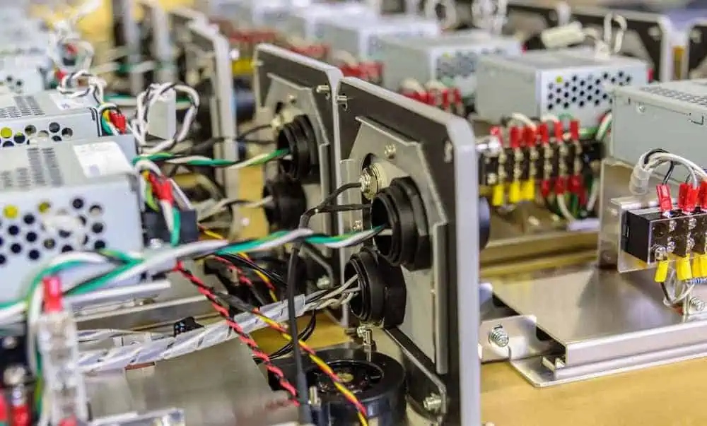
The box build assembly involves all other assembly works that are involved in electromechanical assembly. This is asides from producing printed circuit boards. In addition, the box build can be at times called “systems integration.”
In this article, we will be considering what box build assembly is, what wire harnesses are, installation of sub assemblies. Also, we will consider basic electrical safety testing, electromechanical assembly process and more.
What Does the Box Build Process Entail?
There is always a box build process for every project and this could include different complexity degrees at every step. One step may have to do with placing the PCBA (printed circuit board assembly) in a specific enclosure. Also, other subsequent steps may include a complex task. This includes the connection of the PCBA (printed circuit board assembly) to the display of the user interface.
Furthermore, the most common of all the box build assembly process are installation of the sub-assemblies, installing the other components. It also includes routing the cabling or wire harnesses, as well as fabricating the enclosures.
Giving the electronics manufacturer or contract manufacturer with all the necessary details for the complete box build and product assembly will aid this manufacturer to model the box build assembly process. This box build assembly helps to serve the customer best.
What are the Ways for Shortening the Box Build Assembly Process?
In this section, we will be revealing some items, which form a very significant information. This is given to the Electronic Manufacturing Services (EMS) provider. This information regarding box build assembly can reduce the time lines of the box build assembly. It will also offer an electromechanical assembly of higher quality.
Product Dimensions
The unit’s dimensions include details regarding the weight and size of the assembly. The detail provides the EMS all the important information that will help them to make decisions concerning the way the units should be handled all through the full box build assembly process. Transportation, storage, packaging, as well as shipping are the processes, which are usually influenced and affected by the dimension information.
3D CAD Model
One important aspect of a build box process is visualizing the final product. With the help of a 3D CAD (computer-aided design) model of three dimensions, will be able to offer this type of visualization. In addition, the software packages for the 3D CAD design can be found commonly among the electronics contract manufacturers. Also, these 3D CAD tools could as well convert the computerized drawings in the build instructions. This can help to reduce the complete box build process.
The Bill of Materials (BOM)
This is surely a very important information that is given to the Electronic Manufacturing Services (EMS) provider. You can call it the ingredients, recipe or formula list. This bill of materials (BOM) assists the EMS to comprehend all the main materials and components necessary to be sourced as well as what the client will provide directly.
All the items present on the bill of materials comes with its own associated cost, procurement process, and specific purpose. In addition, this BOM must include details regarding the part description, reference designator, item number, manufacturer part number, manufacturer name, quantity, part type, package, etc.
Furthermore, the bill of materials that is well crafted could assist the Electronic Manufacturing Services (EMS) provider in anticipating the production delays. They can also establish some alternative plans to help with the box build assembly.
The full product assembly could be a very significant physical tool in planning the box build most especially when there are other information sources unavailable. Furthermore, the EMS could often take the rough prototype of the customer and then manufacture many equivalent assemblies quickly.
Also, working with a very skilled team offering electromechanical assembly can help in replicating the complete box build having a minimal documentation from beyond that sample prototype unit which the customer provides.
Use Cases for Testing
Also, the customer must identify the tests that have to be conducted when the box build assembly is ongoing. The use cases necessary for testing could include the functional tests, factory acceptance testing, and visual inspection.
With all electrical devices, one important consideration is safety. The basic testing and labeling testing software loading of all electrical systems involves the flash test and the bond test. Furthermore, experienced EMS providers will offer some guidance regarding the testing types, which has to be performed when the box build is on in optimizing the production time as well as offering an electromechanical assembly that is very safe.
Shipping and Packaging Info
When outlining the way the packaging of the final box build assembly and then shipped even before the start of the production process could offer useful planning information to your electronics manufacturer. The detail lets the EMS make the right decisions regarding the management of the units. Also, this goes through the complete box build assembly process in optimizing the speed of the box build.
The simple and complex box build assembly usually depends on severe requirements gathering. Also, when there is much information to discuss with your electronics manufacturer all through the phase of planning could lead to a safer, higher quality, and faster product.
Rayming PCB & Assembly is focused at developing different custom box build processes, which stands out or are in line with the customer’s objectives. Also, Rayming pcb & assembly makes use of some manufacturing techniques for all the processes and operations in realizing the most appropriate electronic box assemblies.
Conclusion
The box build assembly involves all other assembly works that are involved in electromechanical assembly, asides from producing printed circuit boards. There is always a box build process for every project and this could include different complexity degrees at every step.
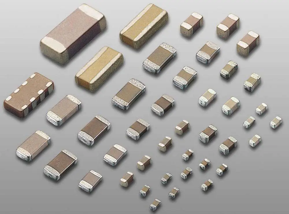
Are you stuck in a design rut, not knowing which capacitor is suitable for your work? In a circuit, all capacitors play the same role of storing charge. However, there are notable differences as you move from one capacitor to another. For example, ceramic capacitors are pretty different from film capacitors. Chip capacitors also differ from any other capacitor type. SMD supercapacitors have been among the best capacitors through the years, as they are applicable in high voltage, high current, and high-frequency applications. However, getting a suitable SMD capacitor from a reliable dealer is advisable. The following are the top 10 SMD capacitor manufacturers in the world.
The company was founded in 1990 by John and Irene Golbeck. Since then, they have been skillfully managing the company, which has led to its tremendous growth. Gama electronics company mainly focuses on producing electronic components later used by assemblers during the fabrication of appliances. In addition, the company undertakes the task of distributing its finished electronic products worldwide.
Company’s Products
Gama electronics mainly focuses on SMD capacitors. However, besides them, the company also deals in other products such as:
The company holds the quality management ISO9001 certification that assures its clients of high-quality, reliable products.
Market
The domestic market of the company’s products comprises customers in fields such as the marine, appliances industry, medicine, automotive manufacturing, etc. In addition, the company distributes its products worldwide through both water and air shipments. Moreover, Gama electronics has a modern US production facility, interfaced with other global alliances. Consequently, the company can sell its products at lower but reasonable prices, giving it a competitive advantage over other companies.
Employees
As one of its strong points, Gama electronics have enough engineers and designers who are in phase with the latest technology. Its products are therefore classy and very efficient as a result.
Founded in 1992, Aerovox has been the leading provider of SMD capacitors. Additionally, the company also deals with other electronic components such as:
Ceramic capacitors
SMD diodes
Film capacitors
Wire-wound resistors
SMD resistors etc.
The company has its headquarters in New Bedford, Massachusetts. Moreover, it has well-developed manufacturing and testing points in India, the USA, and China. Availing their products to their clients worldwide becomes easier as a result.
Certification
Aerovox company holds the 2015 quality management system ISO9001 certification. The certification covers all its manufacturing facilities that use Lean Six Sigma manufacturing processes.
Market
Aerovox is a known company for producing one of the most reliable electronic components in the world. Consequently, this reputation assembles many customers worldwide, giving the company a solid reason to continue. In addition, the company has a wide range of development capabilities, allowing for the provision of intelligent capacitor solutions by the company to its client. Therefore, surpassing the customer’s expectations increases Aerovox’s worldwide client population. Additionally, the three manufacturing and testing points in the three states, China, India, and the USA, aid in producing enough electronic components. The components are later shipped to clients all over the world.
Founded in 2005, RayMing technology is one of the largest manufacturers of SMD capacitors. Additionally, the company deals with the manufacture of other electronic components. These components include SMD resistors, ceramic capacitors, thick and thin film capacitors, SMD diodes, wire–wound resistors, inductors, and switches. In addition, RayMing tech also deals with the manufacture and assembly of printed circuit boards (PCBs). The company’s headquarters are in Asia – Pacific (APAC), specifically in Shenzhen, Guangdong, China
Market
RayMing company is a profit-oriented company that ships its products globally. The primary market consists of the domestic market in the Asia – Pacific region. The rest of the demand comes from the global market. The company’s staff works towards the production of high–quality goods, which will aid in the expansion of the market, hence more profit.
Certification
RayMing company has implemented the QS9000 and ISO9001 quality system certification. The two assure customers of top-quality goods. Consequently, this confidence attracts more clients, increasing the market size. Moreover, the company can brag about an improved quality assurance system and other quality inspection equipment. The equipment aids in the monitoring of the entire production procedure, assuring the dealers of the product’s stability.
Admit refractory was founded in 1997 and has been the leading provider of SMD capacitors, and refractory metals in any form since then. In addition, the company provides such materials as:
Furnace parts
Machined parts
Sputtering targets, etc.
In particular, Admit refractory offers a wide variety of mill forms such as:
Tungsten
Niobium
Tantalum
Powders
Tubes
Wires
Rods
Plates
Sheets
Strips
Foils
Titanium
Molybdenum
The company avails them in the mill forms to fit the client’s specific needs. In addition, the company performs such tasks as the fabrication and manufacturing of industrial components in different fields such as:
Aerospace
Medicine
Defense
Lighting
Moreover, the company manufactures semiconductors as well as electronic components such as:
SMD diodes
Linear resistors
Ceramic capacitors
SMD resistors
Thin film resistors etc.
Admit refractory company has its headquarters in Norristown, Pennsylvania.
Market
With 25 – years of experience, Admit refractory delivers excellent customer service during sales. In addition, the company ensures fast, reliable delivery and delivers goods of high quality. The primary market for the company’s products is the domestic market. However, the company ships its products worldwide to any destination.
Certification
Admit refractory holds a quality management system ISO9001 certification that grants it a good reputation. Consequently, the customers develop confidence in the products of the company.
Cornell Dubilier, a leading capacitor manufacturer, was founded in 1909. The company has its headquarters in Liberty, USA. In addition, Cornell Dubilier company is also known as CDE and offers the following products:
With an experience of over a century, the company is one of the best SMD capacitors manufacturing companies. CDE combines engineering expertise with innovative product technologies, providing reliable SMD capacitors. Moreover, the company produces unique classy capacitors that are applicable to later generations, hence getting a competitive advantage in the power electronics market. In addition, safety agencies such as UL and CSA have recognized the company’s products, assuring customers of no risk while in use.
Certification
CDE company has the quality management system certification ISO9001 that grants it the mandate to manufacture its products in such places as:
South Carolina
Massachusetts
New Bedford
Mexico
Hong Kong
Mexicali
The company then distributes the products manufactured in these places to the worldwide market.
Founded in 1973, High energy corporation is a manufacturing company dealing in the manufacture of SMD capacitors, and other electronic components. The company deals in such products as ceramic high-voltage capacitors, and standard oil-filled capacitors. Additionally, the company manufactures high-frequency SMD capacitors that are applied in commercial and industrial activities. High energy corporation has its headquarters in Parkesburg, Pennsylvania.
Applications of the Company’s Products
SMD capacitors manufactured by this company are used in:
Additionally, temperature compensating capacitors are applicable in heating operations.
Market
Due to the high competition in the electronic market environment, High energy corporation company produces capacitors of all types in various shapes and sizes. Consequently, the products surpass the customers’ requirements and grant the company a competitive advantage. The primary market for the company’s products is the domestic market. However, the company distributes its products worldwide through air and water shipments.
Certification
Having been in operation for 49 years, the company has a lot of experience. It has had several certifications, such as the quality management system certification ISO9001. In addition, it is recognized by RoHS and meets such standards as CSA, CE, IEC, and TUV.
The company was founded in 1997 and is among the largest independent distributors of electronic components in bulk. The company is highly ranked in the global procurement services, making it well recognized worldwide. NetSource tech specializes in locating the obsolete, hard–to–find, EOL (end–of–life), and highly allocated electronic components that have longer lead times. The company’s most popular products are:
Additionally, the company is well known as a dealer in trigger devices, transistors, diodes, converters, amplifiers, as well as passive circuit elements like:
SMD capacitors
Ceramic capacitors
Varistors
Thermistors
Laser diodes
Inductors
Thin film resistors
SMD diodes
SMD resistors etc.
Market
NetSource technology, with its 25 years of experience, has become a worldwide dealer in SMD capacitors for years. With its headquarters in San Clemente, California, the company has a larger market in the domestic market that contributes about 30% of the company’s products market. However, being a worldwide supplier of electronic components, its customers, the electronic assembly companies, are worldwide. The company’s highly skilled staff and current technology meet the customer’s requirements by providing high-quality goods.
Certification
NetSource technology company holds the quality management ISO9001 certification, which guarantees quality goods to the customers. In addition, the RoHS recognizes the company’s products, assuring the customer of safety while using their products.
Founded in 1975, Tecate group, a worldwide SMD capacitors manufacturer and supplier, has its headquarters in San Diego, California. In addition, it has two other stocking locations in Europe and Asia. Moreover, the company manufactures and distributes high-quality SMD capacitors, ultracapacitors, and other electronic components to all its customers worldwide. In addition, the company has its specialty in the following areas:
Additionally, the company offers a wide range of custom components such as SMD diodes, SMD resistors, ceramic capacitors, chip capacitors, etc.
Market
The largest market for the company’s products is the primary domestic market near the headquarters and the distribution points. Moreover, the global market constitutes 40% of the company’s market. Automotive, audio, lighting and medical firms are the company’s major clients, as they employ their products in their daily activities.
Certification
The Tecate group company has the ISO9001 quality management system certification that accords the mandate to distribute its goods throughout the continent. In addition, the company has its products certified by the CE systems.
Founded in 2007, Anhui safe company, a member of the Green international group, has its headquarters in Tongling, Anhui. In addition, it is an electronic company that deals with SMD capacitors, and such electronic components as:
Polyester heat transfer film
MPP (metalized film)
BOPP (polypropene film)
DC link capacitors
Charge controllers
DC-AC automotive converters
AC motor capacitors etc.
Market
With 15 years of experience, the company produces goods of top quality and avails them to the job market at lower but still profitable prices. Moreover, Anhui safe company designs goods for both domestic and overseas shipments. As a result, the company’s products are allowed to enter such markets as UL, TUV, CQC, and VDE.
Certification
Anhui company holds three quality management system certifications, namely:
The company was founded in 2000 in Shanghai, China. Pluspark technology mainly majors in the manufacture and supply of SMD capacitors, and such electronic components as:
Screw terminal capacitors
Radial type capacitors
Chip capacitors
Tantalum capacitors
High voltage capacitors etc.
Market
The main manufacturing point is in Shanghai, China, but its SMD capacitors are distributed to the overseas market, despite having a ready domestic market.
Certification
The company holds two quality management system certifications, ISO14001 and ISO9001. Consequently, customers worldwide trust the quality of the company’s products and feel safe while applying them to consumer electronics equipment.
Conclusion
Faulty electronic circuit components can lead to the failure of an entire circuit, or cause damage to other complementary components. No need to risk, get quality components from enthusiastic dealers in the world. For capacitors in your circuit, get the best SMD capacitors from authorized and reliable manufacturers. The above information makes it possible to understand the top 10 best SMD capacitor producer companies globally. The products, market and certification of each company is well catered for. Consequently, with the above information, the choice of which company’s SMD to incorporate in your setup becomes a walkover. Moreover, the above information gives a variety of other products dealt with by each of the ten companies. With the above information, the question on which SMD company to buy from, is well answered.
The manufacture and assembly of electronic devices and appliances incorporates various electronic components. For instance, in inductive circuits, the main components are inductors. Additionally, SMD inductors are the best type. However, their quality may differ with different manufacturers. Low quality SMD inductors automatically leads to faulty circuits. It is therefore needful that you get them from reliable dealers. The following are the top 10 SMD manufacturers in the world.
Littelfuse
One of SMD inductors’ most well-known manufacturers and distributors is Littelfuse, founded in 1927. The group wants to create a connected, workable, and active world. Littelfuse is based in Chicago, Illinois, in the United States. The group has also established other activity hubs in more than 15 countries. Furthermore, Littelfuse has established fantastic organizations with more than 17,000 partners worldwide.
In addition, the company provides services to more than 100,000 end users globally. Moreover, the firm operates more than 20 functional examination labs globally. With its broad range of SMD inductors fabrication, the company creates effective electronic circuit solutions for its customers.
Products
Littelfuse is a well-known supplier of other electronic products besides SMD Inductors, such as:
Circuit breakers
charge regulators
capacitors
Polyxena devices
cable holders
breaker blocks
DC vehicle connections etc.
Application of Products
The company’s products are used in a variety of industries, including:
Littelfuse can display certifications such as the ABS PGR-8800, ISO14001, and the Quality Administration Framework ISO9001.
Market
The business has a sizable global market and many end customers in all of its activities. Moreover, the net annual agreements for 2021 at Littelfuse came to about 2.08 billion US dollars.
KOA electronics, a well-known SMD inductor producer, was established on June 17th, 1993. The business also handles the duty of distributing its components over the world. The company’s headquarters are in Metropolis Drive, Hunghom, Kowloon, Hong Kong. KOA Electronics is a significant manufacturer with working capital of around 1,550,000 US dollars. Moreover, the company employs over 1000 people, including over 100 staff members.
Products
The company specializes in the production and distribution of the following goods in addition to SMD inductors:
The company has the following certificates in the course of its operations.
ISO9001:2015 quality management system
IATF16949:2016 product certification
ISO14001 Environmental Management System
Market
KOA Electronics (HK) Limited has a well-established home market in the Asia-Pacific (APAC) since it is a wholesale distributor of SMD inductors. However, the business may also take pride in a healthy global market due to many end users in more than 70 countries.
Maxim Integrated, a manufacturer of SMD inductors, was established in 1983 and has a significant impact on fostering design innovation. As a result, many engineering issues are resolved because the necessary electronic components are readily available. The company’s corporate headquarters are in San Jose, California, USA. The business is involved in producing high-performance analog and digital electrical products. Additionally, the company manufactures mixed-signal goods, advancing the designation of smaller and more effective systems.
Products
In addition to SMD inductors, Maxim Integrated is a well-known producer of essential circuit components like:
The company’s products are applied in many fields, such as:
PCB assembly
Manufacture of consumer appliances
Automotive engineering
Networking systems
Renewable energy power plants etc.
Certification
The company has made the following achievements since its establishment:
ISO9001:1984 Quality Management System
ISO14001:1986 Environmental Management System
With its products being recognized by RoHS.
Market
Maxim Integrated Company distributes SMD inductors internationally. The company’s headquarters in San Jose, California, is where the goods are made. The products are then shipped internationally by air and water for distribution. The primary product market for a corporation is the domestic market, specifically the USA. The company employs a large number of individuals—up to 7,100 at most. Consequently, the business can generate a sizable revenue of about US$2.632 billion.
One of the biggest producers and assemblers of SMD inductors and printed circuit boards (PCBs) is Rayming Technology. The business was founded in 2005. The company also engages in the production of various electronic components. SMD resistors, ceramic capacitors, thick and thin film capacitors, wire-wound resistors, diodes, and switches are a few of these parts. The corporation is headquartered in Shenzhen, Guangdong, China, which is part of Asia-Pacific (APAC). High-quality PCB manufacturing and assembly are Rayming Tech’s primary areas of concentration.
Products
Other than SMD inductors, Rayming tech company deals in such electronic products as:
Microcontrollers
Resistors
Diodes
Interface ICs
Application of Products
The following are the main industries where Rayming Technology’s goods are utilized::
PCB fabrication / assembly
Automotive technology
Communication systems
Fabrication of consumer appliances
Transmission systems etc.
Certification
In 2004, the company secured the Quality Management System ISO9001 Certification. Later in the year, the company achieved the ISO14001 Environment Management System certification.
Market
An organization focused on making a profit, RayMing Company exports SMD inductors worldwide. The Asia-Pacific region’s domestic market makes up the primary market. The world market supplies the remainder of the demand. The employees of the business labor to provide high-quality products that will help the market grow and, as a result, generate more profit.
Founded in 1944, Murata is a designer, producer, and supplier of SMD inductors and cutting-edge electronic components. Akira Murata‘s business venture in Nakagyo-Ku, Kyoto, Japan, began as a modest 150m2 factory. The corporation has its main office in Higashikotari, Japan. Moreover, it has other operation points in more than 100 nations.
Products
In addition to SMD inductors, Murata international is also a famous dealer in other components such as:
Capacitors
Resistors
Diodes
Noise suppression products
Thermistors
Ultrasonic sensors
Quartz devices
Timing devices
Varistors etc.
Application of Products
Murata’s products have a wide range of applications. The following are examples of fields of application of the products:
In consumer electronics, including laptops, tablets, smartphones, and other household appliances like vacuum cleaners, refrigerators, and microwave ovens;
In industrial electronics, the components are applied in such areas as:
In addition to industrial uses, the goods are also employed in healthcare technology, such as in developing personal healthcare items like hearing aids, blood glucose meters, and thermometers.
Field of mobility – The products are applied in automotive engineering for such tasks as connectivity, risk reduction, DC-DC converters, etc.
In the enterprise industry, the company avails its products to franchisees, who intend to supply them to consumers.
Certification
Murata company has the following accreditations:
Quality management system certification ISO9001
Environmental management system certification ISO14001
Moreover, Murata’s SMD inductors are recognized by RoHS and meet such standards as CSA, CE, IEC, and TUV.
Market
The company’s several manufacturing locations give it a sizable domestic market. The global market, however, commands the majority of the market.
In 2002, Renesas Electronics was founded in Tokyo, Japan’s Toyosu Forest. The company’s main office is still located in Toyosu, Tokyo. The business’s global operations began in April 2010. SMD inductors and other semiconductor products are the main focus of Renesas Electronics’ research, design, development, manufacturing, sales, and servicing activities. Additionally, about 22,000 employees are working for the organization.
Products
Besides SMD inductors, Renesas electronics corporation deals with the manufacture and sale of other products such as:
– Microcontrollers & microprocessors
– Programmable mixed-signal products
– Sensors
– Ceramic capacitors
– Memory and logic products
– Power management products etc.
Application of Products
Products from the company are used in areas like:
• Communication and computing infrastructure
• Automotive designing and development
• Fabrication of consumer electronics
• Industrial applications such as home automation, factory automation, etc.
• In the Internet of things (IoT), designing of smart cities, smart homes, etc.
In the course of its operation, Renesas Electronics can boast the following certifications:
ISO9001:2002
ISO14001:2003
Moreover, the company’s SMD inductors are RoHS accredited.
Market
Renesas Electronics Corporation sells its goods internationally owing to its numerous operating divisions. As a result, the domestic market comes in second place, with the global market serving as the central market.
The firm Infineon Technologies was established in 1999. The corporation is headquartered in Germany. Moreover, the company has specialized knowledge in the production and marketing of SMD inductors, owing to its 23 years of experience. In addition to its headquarters in Germany, the company operates out of the following three locations:
• Singapore
• Milpitas, California, USA
• Asia-Pacific (APAC) in Tokyo, Japan
Products
Other than SMD inductors, the company also deals with the following products:
• SMD capacitors
• Linear resistors
• Film capacitors
• SMD resistors
• SMD transistors
• Ceramic capacitors etc.
Application of Products
The company’s SMD inductors use the manufacturing of security devices, communication technology, automobile engineering, and other fields. Infineon’s products are also used in a wide range of commercial and consumer gear. The following are the company’s main areas of focus:
Energy efficiency technologies
Internet of things (IoT)
Mobility enhancement.
Certification
Infineon tech holds such merits as ISO9001 Quality Manage System, ISO14001 Environmental Management System, etc.
Market
The company distributes its products globally in the global market in addition to the domestic market, which is its principal market for its goods.
Bourns is an electronics manufacturer established in 1947 and specializes in producing SMD inductors. The corporate headquarters are in Riverside, California, in the United States. In addition, Bourns is a privately held business. It bears the names of its founders, Marlan and Rosemary Bourns. Additionally, Bourn’s company employs nearly 9000 talented employees. Since its founding, the company has opened more than 15 research labs and more than 500 operational locations across the globe. The business also maintains a well-equipped satellite office in Santa Clara, California, in United States.
Products
The company specializes in producing the following electronic components in addition to SMD inductors:
The company’s facilities are certified to ISO/TS16949:2002 and ISO9001:2000. Additionally, Bourns is seeking the TL9000 certification for telecommunications industry-related products.
Market
Bourns has a solid global market because of the substantial number of operation points. The numerous research labs also support ongoing research, giving the researchers access to modern tools. In addition, they have a competitive advantage over other businesses of a similar nature because of the exceptional quality of their products.
Hollyland Group was established in 1975. The business has 47 years of expertise and is now a significant producer of SMD inductors globally. The company is well-known worldwide, including in China, the Middle East, and China, as a maker and distributor of SMD inductors. Hollyland’s Asia-Pacific (APAC) regional headquarters is in Beijing, China. Hollyland Group has built a solid reputation for producing superior SMD inductors throughout its operations. The company employs about 1000 talented people.
Products
Besides SMD inductors, the company also deals in other electronic components such as:
SMD capacitors
Protective thyristors
Ceramic capacitors
SMD resistors
Thermistors
Integrated circuits
Application of Products
The SMD inductors from Hollyland are used in a variety of industries, including:
Appliance manufacture
Automotive electronics
Internet of Things (IoT)
PCB assembly
Consumer electronics
Circuit protection cutouts etc.
Certification
In 1998, the company was accorded the ISO9001 quality system certification by BSI. Additionally, in 2001, the Hollyland group was awarded the automotive quality system certification, ISO/TS16949:2009. Moreover, the company’s products are RoHS accredited and lead-free compliant.
Market
The Asia-Pacific (APAC) region is the most dependable domestic market for Hollyland Company. The business also has a robust web marketing infrastructure that enables networking on a worldwide scale. Additionally, the firm provides services to over 100,000 end users in China and Asia.
John and Irene Golbeck established the business company in 1990. Since then, they have successfully managed the business, which has resulted in its enormous expansion. The Gama electronics company’s primary focus is on producing electronic parts that are later employed by assemblers in the construction of appliances. In addition, the company specializes in producing SMD inductors, being more precise. The business also takes on the responsibility of exporting its finished electronic goods to the international market.
Products
SMD inductors are primarily the focus of Gama electronics. But in addition to those, the company also deals in other goods like:
• ceramic capacitors
• wireless remote controls
• control panels
• switches
• SMD diodes
• custom electronic controllers
• custom electronic assemblies etc.
Certification
The company holds the quality management ISO9001 certification that assures its clients of high-quality, reliable products.
Market
Customers in industries including marine, appliances, medicine, automotive manufacture, etc., make up the domestic market for the company’s products. Additionally, the business ships its goods by water and air worldwide. Gama Electronics also has a cutting-edge US production plant that connects to other international partnerships. As a result, the business can sell its goods for cheaper but fair pricing, giving it a competitive advantage over rival companies.
Conclusion
The above information highlights the best SMD inductors manufacturers in the world. Therefore, in electronic designs, consider acquiring SMD inductors from them, depending on your preference. In addition, the information covers products each company deals with, the various applications, the company’s accreditations, and the market at large.
A computer is a powerful machine that can process large volumes of visual data. Most companies use this technology for industrial and scientific processes requiring accurate pattern recognition.
Examples of these applications include material inspection, object recognition, pattern recognition, electronic component analysis, and the recognition of optical characters, currency, and more. If you’re wondering which type of machine vision system you need, check out our quick guide below.
A line scan camera is good for inspecting webs and cylindrical objects. It has a flat field of view and excels at imaging large objects with high resolution. It can also view through rollers on a conveyor.
These machines help inspect continuous processes and high-speed conveying systems. In addition, they fit into small spaces. Line scan cameras are useful in manufacturing environments where the parts are in constant motion.
Difference from other machines
One of the main differences between line-scan cameras and other types of machine vision systems is the sensitivity of the sensors. As a result, some cameras are better suited for high-speed operation, while others have higher sensitivity.
You can use line-scan cameras to detect defects and read text. However, the sensor’s sensitivity varies greatly, so the choice of the sensor will depend on the tasks you plan to perform.
2D vision robot
Two-dimensional (or 2D) machine vision systems provide area scans of discrete parts. They are the most used machine vision technologies compatible with most vision software packages.
While 2D systems typically feature around 5 MPixels, higher-resolution cameras are increasingly becoming standard products in 2D product lineups. Several factors play a role in the decision between the different resolutions. One factor is speed, while another is cost. Related optics are also crucial in determining the resolution.
3D robotic vision systems
The 3D robot Vision market is highly fragmented. Three-dimensional machine vision systems are fitted with multiple cameras to capture 3-dimensional images of objects. They are accompanied by a robotics application that can give universal robots part-oriented information.
As each camera has different objectives, 3D mapping gives accurate inspection results and accounts for unexpected factors. The 3D mapping capabilities of 3D robot Vision systems make them particularly suitable for metrology, defect detection, and guidance. However, 3D Machine Vision systems have other advantages as well.
Embedded
Embedded vision is becoming an increasingly popular way to automate industrial processes. Unlike traditional vision systems, embedded vision components are typically small and low-cost and you can easily integrate them into various products. As a result, they are the foundation for modern production and intelligent robotic automation.
Embedded vision can identify defects or abnormalities without human interaction. With the help of neural networks, embedded vision systems can determine the appropriate response in a given situation.
How do robots perceive the world? There are several ways that they perceive the environment, and we’ll explore each of them in turn. Let’s start with inference methods. Sensors, Cognition, and Time perception are all essential components of perception.
These factors contribute to the way robots make decisions about their environment. We can think of inference methods as a set of rules that a robot can use to learn and improve its perception.
Inference methods
The active inference is a computational theory for biological agents that formulates every task as an inference problem, requiring the agent to infer the target location of a parking spot from a human observer’s judgments.
This theory was tested on a ground-based robot, which was given the complex task of learning the location of a parking spot from its human observer. To understand how Active inference works, we first need to understand the basic model of an active inference agent.
The active inference is a framework that explains how the brain works. It combines principles of statistics with physics to understand the causal relationships between different behaviors. It can simulate a variety of behaviors, from learning to control and estimation.
Senses
To achieve the same level of interaction as humans, robots must be able to perceive the world physically. While humans have a mental representation of their environment, robots struggle to translate pixel values into semantic objects.
MIT researchers have developed a robot spatial perception model mimics how humans navigate the world. This model has important implications for future robot interaction. Read on to learn more about how robots perceive the world.
Humans can differentiate between bodies at two years old, but the computation required for this is too complex for machines to perform. So Dr. Lanillos devised an algorithm that enabled three robots to distinguish humans from other objects.
The eSMCs project aims to apply cognitive modeling to robots to create better behavior. This research deals with contingencies sensomotoras, or regularities between actions and changes in the sensory variations associated with those actions. This includes, for example, actions like drinking water simultaneously as speaking. Robots are also capable of discriminating between bites and grains of acne. But how do they do this?
Perception is critical to robots’ future performance. Robots must understand their environment to complete tasks such as working in factories, quickly delivering packages in warehouses, exploring Mars, and performing many other tasks.
Time perception
Learning about time perception in robots is essential for many different reasons. First, time is one of the most critical components of our daily lives, and robots are no exception. For instance, dolphins and bats excel at this task because they use echolocation to sense time. They can do this because they are social animals, so they use this information to communicate with other living organisms. Likewise, a robot’s ability to perceive time is vital for many different tasks, including learning to detect and avoid danger.
The arousal-based time perception model suggests that emotional arousal affects time perception. Anger and fearful stimuli evoked overestimation. These findings suggest that these emotions affect the operation of attentional processes, which are responsible for orienting and disengaging attention. The Go/NoGo task may have stimulated noradrenergic pathways and attentional mechanisms to enhance time perception. BIS is also implicated in the process.
Vision guided robots are AV systems that use cameras as secondary feedback signals to control the robot’s movements. This system helps the robot to move more accurately by recognizing objects and environments around it. Here are some examples of VGSs. The XG-X series is a popular choice for this type of AV system. It is a 3D stereo camera fitted with two or more lenses.
3D stereo cameras
Using 3D stereo cameras in a robot vision system is a promising way to improve the accuracy of its range and detection capabilities. A computer vision system is a versatile tool for industrial applications, allowing a robot to recognize and identify objects. However, there is need to first complete a calibration process to make the most of this technology.
Computer vision enables the robot to calculate the 3D coordinates of point clouds on the surface of an object. This data is helpful in 3D building mapping and other applications. In addition, 3D analysis software can also use point clouds to make accurate estimates.
2D cameras
A robot vision system may use 2D cameras to observe parts being handled by the robot. For example, the robot vision randomly picks up a sheet metal part using a suction-cup gripper, and the camera determines its position on the gripper. This information is important to direct the robotic arm to place the part where it belongs. There are several types of cameras and imaging processes available for 2D applications.
The first robot vision systems to use two-dimensional (2D) cameras came into the limelight in the 1990s. These systems provide two-dimensional (x, y) feedback and are best suited for simple, repeatable applications.
2.5D cameras
There are several advantages to installing 2.5D cameras in a robot vision system. First, it reduces the need for cables to be run along the robot arm. It optimizes cycle time and allows the robot to continue working while the vision system captures images.
Moreover, it is possible to get one-shot calibration, which eliminates tedious calibration processes. Robots equipped with 2.5D cameras can address the most demanding applications.
Cobot and LIRAs are cost-effective industrial robot arms that are safe for operation around people. When paired with easy-to-use robot vision systems, you can deploy them quickly. We can also use machine vision in a variety of vision-based applications.
The XG-X series is a highly customizable computer vision system with advanced imaging and programming capabilities. With flowchart programming and an easy system setup, you can customize this computer vision system to meet your requirements.
Its multi-camera hardware supports all KEYENCE cameras, including 3D cameras. This high-resolution system is excellent for challenging inspection applications and can help you solve part variation issues.
The XG-X series system has a 21 MPixel camera with a frame rate of 9 fps. In addition, the camera features a 4/3-inch CMOS image sensor, C-mount lenses, and 3.5 um x 3.5 um pixel size. The advanced hardware and software allow for synchronized lighting for accurate detection.
KUKA’s MotoSight 2D
With its wide range of applications, KUKA’s MotoSight 2d robot vision system can meet the needs of a variety of manufacturing environments. The system is suited for various applications ranging from fast-moving consumer goods to food production.
In addition to its flexibility and ease of integration, the MotoSight system also offers code recognition, simplifying product traceability and quality control. As a result, this technology helps manufacturers protect production output while lowering costs.
Developed to help manufacturers improve efficiency and quality, KEYENCE’s CV-X robotic vision system uses high-speed cameras to detect defects, locate parts, and verify correct assembly.
The system is IP64 and IP67-rated and comes with troubleshooting features that reduce downtime and simplify the replication of systems. In addition, with its built-in character recognition tools, users will no longer need an initial character library.
KEYENCE’s CV-X robotic vision system has many features, including ring-lighting technology, high-speed monochrome cameras, and advanced hardware and vision software. In addition, the CV-X series has an integrated multi-spectrum lighting unit that supports eight wavelengths of light, including infrared, ultraviolet, and visible spectrums.
Summary
Vision guided robots are a type of robotics designed to perform a task. These systems are equipped with cameras that act as secondary feedback signals. As a result, they can help a robot move more accurately. Depending on how the robot sees the environment, it will know where to move. Machine vision can do all this without human assistance. In addition, we can use robot vision in various applications, including robotic surgery and factory production.
An SMD Mosfet is a semiconductor with a spherical shape. It can be either negative or positive and is helpful in electronic circuits. These transistors consist of two parts – an input and an output. The input and output connect using a probe in the center of the device. The center probe transmits electricity, while the rest of the device has a negative charge. This type of transistor is helpful in small circuits.
Types of SMD MOSFET Transistors
What are the types of SMD MOSFET transistors? Let’s find out. In general, these devices can operate at logic voltage levels. For example, the D2Pak case features this type of device. This type is perfect for triggering blades and flag mechanisms. You can also find this type of device on the PROPIC40 board.
The MOS structure of a MOSFET has two P-N junctions flanking the n-channel. The MOSFET is a memory chip storage capacitator and supports a charge-coupled device in image sensor technology. One unique type of MOSFET is the thin-film transistor (TFT), which is made by depositing thin layers of silicon on a substrate. A TFT can be transparent and is commonly helpful in video displays.
The two primary types of MOSFET are the N-channel and the P-channel types. The N-channel MOSFET is essential for regular power applications, while the P-channel version is helpful for high-current applications.
What is the Difference Between N and P-Channel MOSFETs?
The N-channel MOSFET has one main advantage over the P-channel version. An n-channel MOSFET’s mobility is about two-thirds higher than that of a p-channel MOSFET. This means that the current flowing through an n-channel MOSFET is approximately two-thirds higher than in a p-channel MOSFET with the same dimensions.
In addition to being more powerful, the N-channel MOSFET is cheaper to produce. This is because it’s less complicated to make. It’s also easier to produce them in larger quantities. Unlike the P-channel, the N-channel MOSFET doesn’t need a p-channel transistor to function correctly. Both are suitable for applications where the transistor can convert between two different voltages.
The N-channel MOSFET has a positive channel between its source and drain terminals. This enables it to switch on when a positive voltage is applied. A negative voltage must exceed the threshold voltage across the source-drain region to turn the transistor off—the arrow points toward the gate. The P-channel MOSFET, on the other hand, usually is off. The difference between the two types is in the amount of charge that we can apply to the device.
An n-channel MOSFET has two heavily-doped p-type regions, the source, and drain. A thin region between the two gate regions is called the channel. It is where the electrons enter and exit the device. Most of the carriers enter and exit the device through the drain. The drain current reflects this flow of electrons.
What are the materials used to manufacture SMD Mosfet? These components are helpful in many electronic applications, and the taxonomy of these devices is ever-changing. These devices commonly include Metal Electrode Face Bonded (MEFB) components. They are less expensive than flat chips but require special handling during assembly because they tend to roll off the solder pads. Other components include diodes, resistors, capacitors, and other electronic devices.
SMD MOSFETs consists of three layers of components that we solder on different levels. To improve the thermal properties of the device, we fuse the SMDs with lead-free SnAgCu soldering paste. Vapour phase soldering is preferred for SMD because it reduces thermal stress on the substrate. The adhesives are not very good for humid environments but are generally compatible with various substrate materials.
Through-hole MOSFETs feature component leads inserted into holes on the board. The leads of through-hole components run through the board, making them more durable and reliable. They are also more compact, allowing for higher component density. Furthermore, they offer better electrical performance than surface-mounted components. And as a result, they are frequently used in military and aerospace applications. They are also helpful in prototyping and testing applications.
MOSFETs have three pins for controlling the flow of electrical current between the contacts. Electrical voltage controls how the channel appears and what the device does. Semiconductors are easy to manufacture and are highly versatile. In addition to high density and a high switching rate, we can also miniaturize them. These benefits make them ideal for high-volume integration.
If you’re looking for Mosfet manufacturers or suppliers, you can find them in this directory of reliable suppliers and buyers. It provides you with a list of reliable Mosfet companies in China. There are a variety of Mosfet manufacturers and suppliers, and you can choose the one that’s best for you.
Infineon
Infineon is a global semiconductor company that develops and manufactures semiconductors. The company is in Germany, and its subsidiary Infineon China is a Mosfet manufacturer based in the country. In China, the company is active in several markets, including Taiwan. China is a fast-growing market for Infineon. Its growth potential is partly due to its ability to manufacture Mosfets at a lower cost.
Its MOSFET transistor is helpful in power electronics and other applications that require high voltage. It is used in various products and can reduce energy consumption. This type of technology helps reduce CO2 emissions while maximizing energy efficiency. The company’s product range includes products for industrial, automotive, and DC-DC converters. In addition, its MOSFETs are helpful in high-voltage devices, including solar cells.
Silikron Semi
Silikron Semi is a Chinese MOSFET manufacturer. It started in 2007 and has its headquarters in Suzhou. Its capital is 50 million RMB. The company’s objective is to become a world-class design house and to list its products in the domestic stock market in three to five years. Its products are helpful in a wide range of applications, including power conversion systems.
CR Micro
As one of China’s leading local semiconductor companies, CR Micro is active primarily in the IDM mode. It is the top player in the field of power semiconductors in China and has a wide product portfolio. One of its essential products is the MOSFET. Currently, it is the largest manufacturer of MOSFETs in China and has the most comprehensive product range of any local MOSFET company.
Its comprehensive product portfolio includes a wide variety of mainstream MOSFET devices. For example, the company produces planar gate VDMOS and trench gate MOS. As a result, the company’s products can meet the requirements of various applications. Its mission is to provide superior quality MOSFETs for the global market. And, it has a strong R&D team to ensure the quality of its products.
CR Huajing is the largest manufacturer of MOSFET semiconductors in China. Its products are some of the best in the world. Recently, the company won several awards. It won the 12th China Semiconductor Innovative Product Award, the Semiconductor Power Device Innovative Award, and the CITE 2018 Innovative Product and Application Award. In addition, CR Huajing recently became a member of the “Integrated Circuit Industrial Technology Innovation Strategic Alliance.”
The company’s products are widely essential in industrial and consumer applications. Its newest product, the Mosfet microchip, is used in the latest high-end smartphones. The company also provides power semiconductors for the industrial market. Its latest development in this field is the development of high-quality power semiconductors. The company plans to become the world’s top compound and power semiconductor fab capacity by 2023. It is stepping up its efforts in all areas. In the meantime, some domestic MOSFET suppliers have emerged.
WAYON Electronics
As one of the leading suppliers of SMD Mosfets, WAYON Electronics is renowned for its broad range of products. Their portfolio includes small signal MOSFETs ranging from 12V to 250V and complementary versions. They also manufacture SuperJunction MOSFETs, which range in voltage from 600V to 1200V. In addition, they offer both SMD and SOT packages and provide customers with different evaluation boards.
The company has been following the development of the semiconductor industry and establishing a complete industrial ecological chain based on domestic circulation. The company’s product line includes circuit protection, power semiconductors, and mixed-signal ICs.
Jilin Sino-Microeletronics Co., Ltd.
This list of Top 9 SMD Mosfet manufacturers in China includes many companies that have received numerous awards and recognitions in recent years. For example, CR Huajing won the second prize in the National Scientific and Technological Progress Award in 2015, and CR Micro was named one of the Top 10 Semiconductor Manufacturers in China. CR Huajing also won the second prize at the Jiangsu Demonstration Enterprise for Integrating Informationization and Industrialization. Additionally, the company’s products have also won the IC CHINA 2015 Excellent Exhibition Product Award.
In addition to specializing in high-end power appliances, these companies have also branched into the third-generation semiconductor business. Such include introduction of highly durable power MOSFETs to the market for the use in 5G telecom infrastructure. In addition, CR Micro specializes in the research and development of MOSFET products. Meanwhile, BYD has occupied a large share of the Chinese new-energy vehicle (NEV) market.
Micrel
Since the semiconductor market began to recover after the 2000 recession, Micrel has seen robust financial growth. Its annual sales jumped from $104.5 million to $195.1 million, while net income doubled from $24.4 million to $54.4. Despite the recent economic downturn, Micrel still maintains a high level of profitability. However, the company did experience a downturn in 2001. This was largely due to recessive economic conditions, the dot-com collapse, and a huge inventory held by wireless communication customers.
In the late 1990s, Zinn pursued an ambitious financial goal for Micrel. He vowed to make Micrel a $1 billion company by the end of 2003. Naturally, this would require massive expansion. So Micrel diversified its business and expanded its capabilities through acquisitions to meet this goal. Today, Micrel is one of China’s top 10 SMD Mosfet manufacturers.
Micrel began as a small-to-medium-sized semiconductor manufacturer, but by 1996, the company had reached a market revenue of $66 million. The company’s relative size and business savvy allowed it to respond to market changes and capitalize on new opportunities quickly. By the time Micrel made the acquisition, it had already acquired several other companies.
For more than 30 years, Vishay Siliconix has been producing high-quality SMD Mosfets. In addition, the company produces low-voltage power MOSFETs that enable advanced power management in end products. With a focus on automotive markets, Vishay has developed new platforms that offer a better balance between power density and space efficiency. One such technology is its trench MOSFETs, which are becoming increasingly popular in the automotive industry.
Vishay Siliconix has pioneered power semiconductors and leads the industry with its innovative products. Its power MOSFETs improve the efficiency of power management circuitry in end products and reduce space requirements. Its low-voltage power MOSFETs are the industry’s best-selling brands, making portable electronic systems lighter and more efficient. Vishay also produces higher-voltage power MOSFETs that are helpful for industrial applications and power conversion in switches and routers.
Besides MOSFETs, Vishay Siliconix manufactures other types of ICs. For example, their power management products include switchmode regulators, linear regulators, and power management devices. The company has a global presence and continues to expand its product portfolio to meet market demand.
The company’s SO-8 MOSFETs feature compatible SO-8 mounting pads and an exposed rear paddle for thermal transfer. These products are as small as a small serial EEPROM. Their low Rds values and high gate capacitance make them the ideal choice for logic-level applications. They’re also an excellent choice for high-frequency switching.
IR
IR SMD Mosfet manufacturers in China produce power MOSFETs essential in various electronic applications. These products are available in various packages, including through-hole and surface-mount. IR SMD MOSFETs are commonly helpful in computer chips and mobile phones. The company’s high-tech production line specializes in making high-quality power MOSFETs.
The company is a sino-foreign joint venture specializing in quartz crystal, automotive relay, magnetic latching relay, and clocks. QA International Certification Limited has awarded it ISO14000:2003. It is also a supplier of Joyin brand products. Its high-quality employees produce quality products. IR SMD Mosfet manufacturers in China can help you choose the right product for your application.
IR SMD Mosfet manufacturers in China are essential in developing modern electronic products. They have extensive experience and expertise in manufacturing and developing high-quality IR SMD MOSFETs. The company’s innovative technology and high-quality products have helped it become a leading supplier in consumer electronics, television, and power supply applications. In addition to IR SMD Mosfets, the company manufactures pressure sensor chip solutions.
Summary
SMD Mosfet is an excellent semiconductor product that we can use for various kinds of applications. It consists of a metal substrate and a semiconductor. Its small size and low cost make it easy to integrate with other electronics. The main driving forces of the MOSFET market in China are new energy vehicles, consumer electronics, home appliances, and aerospace. China is the world’s largest consumer and producer of automobiles, and it also has the largest manufacturing base for electronic products and OEMs.
The Internet of Things (IoT) is a network of connected devices and systems that collect and exchange data. The data generated by IoT devices can help businesses evaluate processes and identify inefficiencies. The connected smart elements can also help enterprises to monitor their premises and track their customers. This data can help companies develop more personalized customer experiences and optimize their supply chains.
The Internet of Things is a network of connected objects that can monitor and record data in real-time. These objects are self-contained computers with internet IP addresses. They gather data using built-in sensors and transmit it over the internet, often without human intervention. The IoT objects may be as simple as a monitoring device or as complex as self-controlling machinery.
The benefits of IoT are widespread, especially in the public sector and service-related environments. For example, government-owned utilities can use IoT-based applications to warn their users of outages. The data collected by these applications can also help utilities identify outages and deploy resources to assist with recovery.
The Internet of Things can also help improve worker safety. For example, IoT sensors can alert employees of environmental conditions and hazardous events. These sensors can also help physicians monitor patients remotely.
The IoT can help manage and predict natural disasters. For example, we can automate monitoring carbon content and temperature in forests. We then share this information with a common monitoring hub, which can notify emergency services or a control room. Having this information is very helpful for preventing disasters. The IoT can also benefit the home, where various smart devices can monitor temperature and lighting.
The Internet of Things is a network of embedded devices connected to the internet. It enables a smart device to interact, collaborate, and learn from one another. One of the industries that have embraced IoT is wearable technology. Some examples of this technology include Fit Bits and smartwatches.
Smart buildings are another example of IoT use cases. They can help control the temperature of a room or an entire building. They can also detect the number of occupants in a room or office. This means they can turn on the air conditioner when necessary. A smart farming system using IoT can monitor light, temperature, and soil moisture. The data can also help automate irrigation systems. Smart cities are also a great way to alleviate traffic and address environmental issues like pollution by coming up with an air pollution monitoring system.
As more devices connect, the IoT becomes more critical for organizations and businesses. It helps organizations operate more efficiently, understand customers better, and improve decision-making processes. These improvements are beneficial for everyone.
When writing code, IoT engineers typically use one of three languages: Python, JavaScript, or C#/.NET. However, some IoT projects require more complex languages. For example, some IoT engineers are more comfortable with JavaScript, and others prefer Python or C#.
To become an IoT engineer, you should first understand the entire development process. Then, after understanding the development process, you can select a segment to focus on. This is an exciting field with much potential, but you must put in the necessary time and effort to get it right.
One of the main challenges of developing IoT systems is security. A security breach in an IoT system can lead to a massive data breach. As the number of connected devices increases, hackers are increasingly likely to intercept private information. Additionally, there is currently no international standard for the compatibility of IoT systems.
For example, Apple’s iOS devices can become the hub of a home network of sensors. As a result, the Apple HomeKit platform integrates data feeds from a connected device’s network, making it possible for users to focus on specific tasks. Similarly, Amazon’s Kinesis platform can be helpful for this purpose.
IoT developers often use C++. These languages are popular for IoT development because they are easy to understand, powerful, and flexible. They are also incredibly affordable.
Getting involved in IoT projects can be a rewarding experience. As more devices and applications become connected, we realize economies of scale. In addition, software and hardware strike the right balance between functionality and cost, enabling the development of a broader range of products at lower costs. This allows companies to profit from the first wave of IoT devices and develop new hardware products that plug into the system.
To get started, you should consider the business needs your IoT product or solution will address. Once you’ve identified the needs, you should organize your ideas and pre-existing research solutions. One option is to use a device management solution, which can serve as a foundation for your IOT project ideas. Depending on the needs of your business, you may find that device management software provides a highly customizable platform for your IoT development.
Skills
IoT projects require a wide range of skills, from a smart cradle system to software engineering to data analytics. However, the right technical lead can lead to an effective IoT project that benefits your business. Experts in this field may cost a lot, but they can make a difference. They will be able to help you make technology decisions, understand customer requirements, and create communication systems. They can also help you navigate the complicated world of IoT, including multiple software types.
The right programming language can help you get started in IoT projects. For example, C is an excellent choice for IoT projects as it does not require a lot of processing power, but it’s a powerful language and can be helpful on some of the most advanced embedded systems. In addition, you might want to consider languages including Java, Swift, and PHP. You’ll also need to be familiar with web development to design user interfaces for IoT devices.
Niche
The IoT market is booming, and many niches exist in this emerging field. If you have a strong background in statistics, you may want to pursue a career in this niche. However, you’ll also need a deep understanding of network architecture. This is necessary to ensure that IoT devices are safe from hackers. In addition, understanding how to run penetration tests and keep an eye out for network loopholes is also essential.
The IoT market has many applications, including in manufacturing. For example, IoT in manufacturing can reduce downtime and help companies plan maintenance work in advance. Likewise, IoT can improve customer experience. For example, IoT-enabled tractors can track the locations of all other vehicles in a fleet and ensure that the tractors do not overlap when seeding soil.
If you’re interested in getting into the IoT market, the best thing you can do is get training. Training in this industry can give you a leg up over your competition, and you’ll be able to build a career around it.
MQTT is an open-source protocol that can be helpful in-home automation projects. It can be beneficial with low-cost development boards such as the Raspberry Pi. The Raspberry Pi has a Mosquitto broker, which is essential to the MQTT protocol. It also runs Node-RED, a Home Automation Platform that supports MQTT. Using Node-RED, you can create a network of MQTT-enabled devices, such as sensors. This software allows you to set up buttons to control outputs and chart display sensor readings.
Smart Irrigation Using Raspberry Pi
A smart irrigation system uses sensors and microcontrollers to optimize irrigation. The system can monitor soil moisture, temperature, and PH rate. It can also alert the user when the threshold value goes down.
Fault Diagnosis and Small Wind Turbine Monitoring in IoT
A key element of fault diagnosis in small wind turbines is monitoring gearbox gearboxes. This is critical for extending turbine life and reducing maintenance costs. In addition, control and condition monitoring systems play essential roles in detecting and repairing failures.
IoT-Based Light Dimming and Speed Controller
A smart IoT-based light dimmer is an excellent way to lower electricity bills and conserve fossil fuels. One can set it up to automatically control the brightness of light, reduce the speed of fans, and adjust the speed of lights according to the time of day. This innovative gadget can also be helpful in factories to control the speed of AC appliances.
IoT-Based Smart Grid System
An IoT Based Smart Energy Grid System is an energy management system that uses Internet of Things (IoT) technology to monitor and control the system. It can help improve system reliability, efficiency, and sustainability. IoT technologies can also improve system security and congestion management.
Smart Wireless Water Meter With Web DB IoT Projects
A Smart Wireless Water Meter is a device that monitors water consumption. The device can help control water distribution and help save water. It can also detect spills or overconsumption. The project involves a Raspberry Pi implementation, which stores and uploads water consumption details into a database. The system also incorporates a limit-based slab system that controls water distribution.
IoT-Based Motion Detector Using Cayenne
Cayenne is a drag-and-drop IoT development platform that empowers designers, engineers, and developers to create a new device in minutes. It also offers a rule engine that powers automated decision-making and asset tracking. It also includes tools that visualize real-time data.
Monitor Live Temperature Through IBM Bluemix
Monitoring live temperature in your home can be done with the help of IBM Bluemix. This cloud platform supports several programming languages and services that help you develop, run, and manage applications. You can also use IBM Bluemix to connect multiple devices and collect data. For example, using the IBM Bluemix platform, you can build a weather app or even a remote vehicle monitoring system.
Using an ESP8266 microcontroller with NodeMCU, you can implement an IoT smart home automation system. This system can control four home appliances with a few buttons. The app also allows you to monitor the status of these appliances.
ESP8266 IoT Energy Monitor and Over Current Cut-Off
The ESP8266 IoT Energy Monitor & Over Current Cut-off is a WiFi-based IoT device that can detect the current of AC appliances and break the circuit accordingly. The device connects to a home Wi-Fi network and displays a power consumption graph.
IoT Mesh Network smart Agriculture System
An IoT Mesh Network Agriculture System uses data generated by sensors and devices to control and monitor farming processes. For example, it can control the level of large tanks which store fuel, smart irrigation system, fertilizer, or livestock feed. The system can also provide real-time feedback about the condition of a field through a web browser interface. The information may then help control wired or wireless devices on the farm.
IoT-Based Smart Home Controller Using Blynk
An IoT-based intelligent home controller is a software program that lets you control and monitors several connected home appliances. You can set up the controller using an app available for IOS and Android devices. This smart home controller can also monitor your home’s temperature and humidity levels. In addition, the application can display the status of your devices on a graphic display on your smartphone.
Brain Controlled IoT Using EEG Signals
The technology for brain-controlled IoT is a promising development with numerous applications. For example, a user may be able to control a lighting fixture using an EEG signal. In addition, an IoT-enabled wireless actuation network can allow users to interact with their environment.
Control TV With Alexa IoT TV Controller
You can use Alexa to control your television. Unlike most TVs, Alexa is in most of them, but you can buy a Fire TV stick that is compatible with the device. You can also use an IR remote to control your TV, allowing you to operate it simply by speaking into the remote.
IoT Wi-Fi Temperature-Logging System
When it comes to temperature monitoring, an IoT Wi-Fi Temperature-logging system becomes an excellent choice for many different applications. Not only does it eliminate the need for a gateway device, but it also provides an option allowing users to use the device from any location. Cellular and Bluetooth devices, on the other hand, have limited range and can incur extra costs.
If you’ve ever been to a mall, you’ve probably seen the Knightscope security robot, which uses face recognition to track people and report security violations. Unfortunately, although malls are public places, there is little regulation and transparency around the data they collect, which may make them risky for personal data.
SLN-ALEXA-IOT – The Tiniest Alexa-Controlled IoT Device For Your Home
If you are looking for an Alexa-controlled IoT device for your home, look no further. SLN’s SLN-ALEXA-IoT is a solution development kit that provides the capabilities of an Amazon Echo device. It connects to your home Wi-Fi network and allows you to control other connected gadgets. It also has a wake-word feature that will enable you to activate the device with a voice command.
IoT Mesh Enabled Environment Monitoring Devices
IoT Mesh-enabled Environment Monitoring Device (EMD) technology is an essential component of the Internet of Things (IoT). This type of technology enables devices to communicate with each other through a wireless mesh network. In addition, the technology allows devices to collect and analyze data from multiple locations. The resulting data can be helpful for a variety of purposes.
IoT Touch Switch Based on e-Ink Technology
IoT Touch Switch, based on ‘e-ink’ technology, is power-efficient way of controling connected devices. Instead of traditional LED or OLED lights, e-ink uses electrically activated ink molecules that remain on the display even after the power is off. As a result, the device can be helpful for various purposes, including smart homes and digital signage.
IoT-Based Automated Table Lamps
The IoT-Based Automated Table Lamp is a smart lamp controlled using an app. It uses three different kinds of LEDs and has five channels. The LEDs can be either cold or warm, and we can control each channel individually.
Low-Cost IoT Solid State Relay
Solid-state relays are inexpensive compared to traditional relays and can be helpful for many applications. These devices feature two large screw terminals and accept wires of up to 12 AWG. In addition, the RC filter and varistor snubber circuits are essential to any solid-state relay. These components absorb surges and suppress excessive transient voltages to prevent overload and failure.
IoT Smart Traffic Management System
IoT smart traffic management system is a powerful tool to manage traffic and improve mobility. It uses video cameras and sensors to count the number of vehicles on the road, alert emergency personnel, and extend green light durations. This technology is not only helpful in improving traffic management but can also reduce accidents.
IoT Smart Parking System
The IoT Smart parking system uses sensors to direct vehicles to available parking spots. The microcontroller transmits this information to the cloud. The cloud computing service reads this data and displays it on a user interface. The user can see which parking spots are occupied and which ones are free.
The Future of IoT integrates various technologies and devices to improve the human experience. These devices can help improve security, comfort, and productivity. Smart homes are a prime example of this technology. They can control lighting and door locks using face recognition technology and even control gardens by understanding soil conditions and triggering irrigation systems.
The Future of IoT is also changing the way companies operate. Companies must take security seriously in a world where data is more accessible than ever before. This means improving security and privacy. Companies need to ensure that consumers have control over their data and that companies aren’t tracking them.
Smart farming is another example of how IoT can help save money. In the future, smart farming will lead to over 5.6 trillion dollars of savings worldwide by 2050. Furthermore, by 2020, 75% of new cars will be equipped with built-in IoT connectivity, reducing car crashes, time spent in traffic jams, and parking.
As the Internet of Things continues to expand, applications are nearly limitless. Using AI and Machine Learning, it is possible to turn ordinary devices into working IoT equipment. The next big leap for IoT will be the integration of IoT with Big Data Analysis and Artificial Intelligence. In this way, devices can send data to a cloud, where software processes it and pushes it to perform specific actions based on the results. For example, a house sensor can send temperature data to a program that turns on the air conditioner.
Machine learning
Machine learning is a powerful tool that helps to detect patterns from large volumes of data. It can often replace or supplement manual processes, allowing for new insights and advanced automation capabilities. Moreover, machine learning is becoming an essential component of IoT solutions. Its predictive capabilities can help make decisions and make the world smarter.
Combining IoT and ML helps companies automate routine business processes. For instance, businesses can streamline record-keeping, schedule workers, and even run marketing campaigns. Machine-learning algorithms analyze the data and suggest ways to improve processes. For example, IoT sensors can identify areas where resources are depleted or under-utilized. They can also help limit energy consumption and suggest new workflows.
The IoT and AI are two powerful technologies that can enhance the efficiency and productivity of organizations. IoT devices can collect vast amounts of data from their environment, and artificial intelligence algorithms can extract valuable information. These technologies are highly versatile and will benefit organizations of all sizes. They will change different industries over the next few decades.
The growth of IoT technology enables organizations to improve productivity, safety, and use of resources. It is also fueling the development of AI. AI technology can help identify and analyze data from IoT devices, enabling manufacturers to send service notifications and prevent crashes.
Instant feedback
Instant feedback can distinguish between a successful product and one that fails to meet consumer expectations. With the help of IoT devices, brands can monitor consumer behavior and adapt marketing campaigns to meet those needs. This allows marketers to tailor their messages and personalize the shopping experience. But, first, it is essential to reassure consumers that their privacy is secure.
The use of IoT technology is becoming more prevalent in various industries. It has the potential to increase customer service and accelerate the R&D services of an enterprise. Sensors, diagnostics, and insights from multiple devices allow businesses to understand customer needs and preferences comprehensively. With this information, businesses can better design their products and improve customer service. This will ultimately boost their revenues and drive growth in the market.
Cybersecurity
The future of cybersecurity is highly dependent on the IoT. With an increasing number of connected devices, the attack surface is expanding. As such, security professionals must become better at managing these connected devices’ threats. These devices are endpoints in the communications chain, which starts with a human being and ends with cloud platforms and data centers. Because of this, it is essential to protect the data and information that these devices generate.
Unfortunately, many IoT gadgets do not have cybersecurity protection and depend on open-source software platforms. People do not check them for cybersecurity, and vulnerabilities can persist in multiple versions. This makes them targets for zero-day attacks, which exploit a vulnerability before the vendor can fix it. Moreover, these devices are extremely susceptible to hacking, and if they’re not secured, they can cause a massive security breach.
V2X connectivity
The future of connected vehicles depends on V2X connectivity. It allows cars to communicate with other vehicles, as well as other infrastructures, for better safety and traffic efficiency. In addition, vehicles with V2X connectivity can improve the passenger experience by adding in-car entertainment. For example, it will allow driverless cars to entertain drivetime radio and onboard video. V2X technology will also enable a steady 5G connection within the car.
5G networks can support real-time applications. Their speed can approach 20Gbps, requiring minimal application overhead. In addition, the underlying infrastructure must handle large amounts of data and support thousands of V2X clients.
The use of IoT in the healthcare sector could have a profound impact on patient care. For example, connected devices could track patients’ health in real-time, which could help in emergencies. These devices could connect to smartphone apps and provide data on blood pressure, oxygen levels, blood sugar, weight, and ECGs. A designated person could then use the data to provide appropriate treatment. This could include a physician, an insurance company, a participating health firm, or an external consultant.
IoT could improve patient care by streamlining procedures and processes in the healthcare sector. For example, it could help diagnose diabetes and other health problems, improve patient engagement, and improve contact lenses and insulin delivery. As a result, patients will receive help faster and more accurately, and doctors can use accurate data in real time.
IoT Projects Summary
IoT projects enable organizations to use data more effectively and efficiently to make better decisions. These systems have a broad range of applications and are essential for organizations in many industries. For example, these technologies can track inventory, improve operations and customer service, and create new business models. As a result, these technologies are becoming an increasingly valuable part of the global economy.
For example, smart buildings can reduce energy bills by automatically adjusting the temperature. They can also detect the number of people in a room, conference room, or office and automatically switch on the air conditioning when occupancy reaches a certain level. Similarly, smart farming systems can monitor temperature, light, and soil moisture and automate irrigation systems. Smart cities also have the potential to improve public health with the health monitoring system and ease traffic congestion.
One fundamental way to unlock IoT’s true potential is to work with experienced business analysts. These analysts can use various software tools to analyze data. They can then generate graphs, documents, and visualizations. Ultimately, they can help companies make informed decisions and save valuable capital.
As IoT projects develop, developers must consider the ethical and legal issues associated with these technologies. As a result, they must be careful to ensure that they do not create a liability. Furthermore, IoT developers must be aware of the need to protect data and privacy.
Have you witnessed the revolutionary progression of mobile electronic components? The manufacture of small and smart electronic devices can be pretty complicated. However, the presence of versatile printed circuit boards has made it easier to fabricate sophisticated electronic components. As a result, many industries are incorporating flex PCBs to manufacture portable multi-functional devices. Flex PCBs are also very efficient in static and dynamic electronic devices. Oshpark company is among the most famous manufacturers of flex PCBs. The information below explains more about Oshpark and its flex PCBs.
Oshpark Company
Founded in 2012, Oshpark is an American electronics manufacturer headquartered in Lake Oswego, Oregon. Additionally, the company has an employee population of between 6 and 10 people. Moreover, the company’s revenue is between I million and 5 million US dollars. In addition, the company has become a famous manufacturer of rigid, rigid-flex, and flex PCBs. Furthermore, the company also manufactures lead-free boards with ENIG finish. Oshpark then ships these PCBs to any country in the world for free.
Oshpark uses Cloudflare, Fastly, Cloudflare CDN, and Google Hosted Libraries technologies for content delivery.
The company also uses the following libraries and frameworks; jQuery, Ruby on Rails, and Modernizr technologies.
Oshpark uses three web accelerators: Varnish, Cloudflare Website Optimization, and Cloudflare Rocket Loader.
Oshpark flex PCB types
The following are the types of PCBs that the company manufactures:
Two-Layer PCBs-For easy identification during shipping, all two-layer boards have a purple mask over the bare copper, FR$ substrate, and ENIG (immersion gold) finish. In addition, the following are the minimum design rules for two-layer flex PCBs:
For Oshpark prototype PCBs, the board has a thickness of 63mil (1.6mm) and a copper weight of 1oz. Moreover, a set of 3 PCBs cost $5 per square inch and require 12 shipping days. Additionally, a super swift PCB board has a thickness of 63mil (1.6mm) and a copper weight of 1oz. Therefore, a set of 3 boards costs $10 per square inch and require five business days to ship. Furthermore, an Oshpark’s flex PCB has a thickness of 4mil (0.1016mm) for the core and 8mil(0.2032mm) for the stack-up. In addition, the board has a copper weight of 1oz, and a set of three such panels costs $10 per square inch.
Equally important is that a 2oz PCB has a thickness of 32mil (0.8mm) and a copper weight of 2oz. Therefore, a set of 3 boards costs $5 per square inch and requires between 2 and 3 weeks to ship. Again, one Oshpark’s After Dark PCB has a thickness of 63mil (1.6mm) and a copper weight of 1oz. In addition, a set of 3 boards costs $5 per square inch and requires three weeks to ship. Finally, a medium-run PCB has a thickness of 63mil (1.6mm) and a copper weight of 1oz. Moreover, to a maximum of 100 square inches, a set of 10 boards costs $1 per square inch and requires 15 days to ship. Also, the company provides one-sided panels through any of their 2-layer services.
Four-layer PCBs –4-layer boards have purple masks over bare copper, ENIG (immersion gold) finish, and FR408 substrate. Moreover, 4-layer PCBs have the following minimum design rules:
5mil (0.127mm) trace width
4mil (0.1016mm) annular ring
5mil (0.127mm) trace clearance
10mil (0.254mm) drill size.
However, four-layer PCBs do not support buried or blind vias.
PCB specifications
Oshpark manufacturers only two types of four-layer PCBs: prototype and medium run. A prototype PCB has a thickness of 63mil (1.6mm) and a copper weight of 1oz for the outer board and 0.5oz for the inner panel. Additionally, a set of 3 boards costs $10 per square inch and require between 9 and 12 days to ship. Similarly, a medium-run PCB has a thickness of 63mil (1.6mm) and a copper weight of 1oz for the outer board and 0.5oz for the inner panel. However, a set of 3 boards costs $2 per square inch and require between 9 and 12 days to ship. Furthermore, the company can only send a maximum of 100 square inches of medium-run PCB boards at a go.
Six-layer boards- A six-layer Oshpark flex PCB board ship with a purple mask over bare copper, ENIG (immersion gold) finish, and FR408 substrate. In addition, six-layer flex PCBs have the following distinctive features:
5mil (0.127mm) trace width
4mil (0.1016mm) annular ring
8mil (0.2032mm) drill size
5mil (0.127mm) trace clearance
Furthermore, 6-layer Oshpark flex PCBs do not support buried or blind vias.
The company manufacturers only prototype 6-layer flex PCBs. The 6-layer prototype flex PCB has a thickness of 63mil (1.6mm). Moreover, the board has a copper weight of 1oz for the outer layer and 0.5oz for the inner layer. In addition, a set of 3 boards costs $15 per square inch and require 14 days to ship.
Bend Radius Of Oshpark flex PCBs
The bend radius of a static or dynamic flex PCB depends on the thickness of all the board layers undergoing bending. To get the flex PCB’s bend radius, multiply the bend ratio by the board’s thickness. A static bend occurs when you bend the flex PCB into a particular shape and mount it in its bent position. On the other hand, a dynamic bend occurs when the flex PCB undergoes a bend/straighten cycle. For a dynamic bend, the bend radius is challenging to estimate. However, keeping dynamic bends large minimizes wear during operation. On the other hand, sharp, dynamic bends result in quick PCB failure.
Advantages Of Oshpark Flex PCB circuits
Flex PCBs offer numerous advantages in the fabrication and operation of modern electronics. The following are the merits of Oshpark flex PCBs:
Due to their 360° bendability, they easily fit in dynamic applications such as medical and industrial fields.
Owing to their flexible design, they can endure extreme industrial conditions such as high pressure, high temperature, strong vibration, toxic chemicals, etc.
Flex PCBs are lighter and smaller in size. Hence, the flex PCBs are suitable for modern mobile electronic applications.
They are light, and therefore you can stack them over each other, increasing their mobility.
. Oshpark flex PCBs are more durable due to their high resistance to bending cycles.
They make connecting complex inner parts of electronic devices easier due to their versatile nature.
Oshpark flex PCBs are generally applicable in static and dynamic electronic applications.
Conclusion
From the above details, it is possible to understand Oshpark electronics manufacturing company and its flex PCBs. Due to their versatility in current electronics, flex PCBs are essential. In addition, they offer solid electronic solutions in static and dynamic electronic environments. Therefore, consider flex PCBs if you are unsure of the best PCBs for your designs.
If you’re in the market for a new connector, you’ve probably been wondering what you should look for. Here are some things to consider when purchasing a Molex FPC or FFC connector: 0.3-millimeter pitch, Compact design, Double bottom contact, versatility, and more. We’ve also broken down the various features and benefits of the FPC/FFC connector for your specific application.
0.3 mm pitch
The Molex FPC 0.3 m pitch series features a 37-way, single-row surface mount device with a solder termination method. The housing consist of thermoplastic, and the contacts consist of copper alloy. They have a 200-mA electrical rating. Molex FPC can be helpful in electrical connections for computers, printers, and other applications. They can also be essential for connecting cables and printed circuit boards.
The Molex FPC 0.3 m pitch connector series is an excellent option for robotic and automatic SMT processes. Its unique design features allow for secure mating in just one step, reducing the possibility of human error. In addition, the connectors feature a wide alignment guide and auto-lock mechanisms. The connectors also feature a wide gap for ease of cable insertion and a larger area to hold the actuator.
The Double Bottom Contact (DBC) FFC/FPC Connector from Molex has two lower contacts per circuit for superior contact reliability. In addition, these connectors are available with either push-style or flip-style actuators to fit various space and design requirements. Whether designing a high-end computer, automotive, or consumer electronic product, FFC/FPC connectors provide a cost-effective solution for tight-packaging applications.
The Easy-On 1.0 mm FFC/FPC connector has a unique double bottom contact cable earlobe locking mechanism to minimize wear and ensure a clean mating connection. This connector is suitable for consumer products and high-density applications. Its slim design makes it easy to handle and has a mating height of 1.90 mm. In addition, its double bottom contacts enable it to meet the needs of even the tightest of applications.
Double bottom contact FPC connectors are available in various pitches. The 0.25mm pitch design saves 40 percent of PCB space and is ideal for mobile equipment. A Zero Insertion Force (ZIF) connector provides the smallest overall size. One of the benefits of this connector is its reduced installation time. In addition, its SMT ZIF design allows it to fit into tight spaces and save space while making connections.
Easy-On FFC/FPC connectors are easy to use and secure with minimal warpage. They can be mated easily, making them ideal for fully automated and robotic SMT processes. Featuring a wide alignment guide, Easy-On connectors reduce the risk of mismating. The Easy-On FFC/FPC connectors can also be helpful in automated assembly processes. Another great benefit is that they can be fully field-terminated.
Compact design
The FPC connector has a compact design. Its depth is 3.20mm. As a result, it can save space on PCBs. It also offers the largest upward range of circuit sizes, 53. To learn more about this connector, visit Heilind’s website. This product is available in various circuit sizes and pitches and has the same tolerances as the standard 0.25mm pitch Molex connectors.
The Molex FPC is a 17-way flexible printed circuit connector with a liquid-crystal polymer housing. This provides excellent flexibility and durability. It also features double-bottom contact terminals for electrical reliability. The low-profile design of the Molex FPC connector allows for easy integration into small enclosures. In addition, the connector is compact and won’t interfere with the circuit components. Its double-bottom contact terminals also prevent dust from collecting on the terminals.
Molex has long led the industry with its innovative microminiature connectors. This innovative technology provides high-density signals, space-saving design, and durability. Whether you need a connector for high-speed data transmission, wireless connectivity, or mobile communication, you can find the perfect Molex connector for your application. Its product range includes cables in 0.35mm spacing and 42 AWG. Its micro-products offer the highest quality content, uncompressed digital connection, and superior signal integrity.
The Easy-On FFC/FPC connectors are the latest addition to Molex’s product line. The connectors have double bottom contact cable earlobe locking mechanisms that ensure a tight mating connection and minimize wear and tear on the connector. These connectors are ideal for consumer electronics, medical devices, and automotive products. They are also compatible with standard Molex connectors. As a result, they can be helpful in applications where space is at a premium.
The versatility of Molex FPC connectors is unparalleled. The company offers a variety of connector styles with terminal pitches ranging from 0.5 mm to 1.0 mm. Its products are helpful for various applications, from wireless earbuds to automotive. Moreover, it offers different connector styles to meet the needs of various industries. One of these styles is the easy-on FFC/FPC connector, which we can plug into a car dashboard or a smartphone. Moreover, it also features a one-touch connection mechanism. Its versatility is further enhanced by its features, including a small footprint, a low weight, and high reliability.
In addition, it offers easy mating with its One-Touch connectors. These connectors feature an auto-lock mechanism and a wide alignment guide, which minimizes mismating due to human error. They also support a high-speed robotic assembly process. In addition, they can withstand a wide range of operating temperatures, from -40degC to 125degC. This feature makes Molex FFC/FPC connectors versatile enough to be used in various industrial applications.
High-speed, flexible printed circuit assemblies, offer flexibility in mounting and assembly. These assemblies consist of flexible and rigid substrates laminated together. These flexible printed circuits have both flexibility and support properties, making them an excellent choice for many applications, including mobile electronics, three-dimensional wiring, and industrial control panels. Molex high-speed FPC assemblies are the right solution if you need flexible and robust packaging.
The Molex high-speed FPC assembly includes a printed circuit board and a surface-mount strip of metal. The first end of the strip is positioned on the printed circuit board, while the second is attached to the housing through a surface-mount attachment structure. A printed circuit substrate member includes signal and ground conductors.
Molex offers a variety of high-speed FPC assemblies, including high-speed midplane and backplane solutions. These high-speed FPC assemblies are ideal for increased density and optimal data rates. In addition, Molex offers various applications and solutions, including voice and data applications and automotive and industrial environments.
Flexible printed circuit assemblies are a great way to connect two pieces of equipment. They can be slim, water-resistant, and more versatile than traditional wires and cables. In addition, because they can be stacked close together, they are a practical solution for various electronic applications. The Molex FPC connector line has a variety of connector styles and configurations, making it easy for you to find the right one for your specific needs.
Next-generation electronics require manufacturing technologies that maximize space, reduce weight, and provide more capabilities. For example, Molex’s Laser Direct Structuring (LDS) technology enables designers to design antennas in 3D and transfer them from CAD data directly to a molded carrier.
The standardization in the electrical and electronics industry has made it possible for through-hole components to always have a surface-mount equivalent for circuit boards. Designers and engineers have several alternatives for common components that are in a standard footprint. Therefore, designers can source large volumes of comparable components from several manufacturers and replace a component if it isn’t available.
SMD components feature common land patterns and package sizes. The ECAD software can help to replace obsolete SMD components. The 0603 SMD passives are very popular in the electronics industry. Also, the low price, small land area, and ease of assembly of 0603 SMD makes it a popular choice among designers.
SMDs feature several dimensions. The size and shape of SMT resistors are usually standardized. Most manufacturers integrate the JEDEC standards. A numerical code like 1206, 1210, and 0603 indicates the size of SMD resistors. The SMD package code can be in metric or imperial units. Generally, the imperial code is widely used to specify the package size.
However, designers use the metric dimensions during PCB design. The size of the SMD resistor utilized majorly depends on the minimum feature size of the PCB, the limitations of pick-and-place equipment, and the required power rating. There are several specifications and dimensions of surface mount packages.
What is 0603 SMD?
0603 is a numerical code that indicates the size of SMD resistors. This code specifies the height and width of the SMD package. Therefore, 0603 SMD means that an SMD packages features 0.060” in length and 0.030” width. Furthermore, the SMD package footprints feature two different sizing and naming standards that indicate footprints for 0603 components in imperial and metric units.
Therefore, the 0603 SMD component generally refers to the imperial version of a 0603 package footprint. Also, the 0603 SMD metric package features similar dimensions as a 0201 imperial package.
The IPC 7351 standard offers some restrictions on land patterns and pad sizes. As a result, not all 0603 SMDs feature similar dimensions. This is a great idea for designers that need to verify the dimension of the 0603’s datasheet to know if it matches the typical sizing. Therefore, designers might encounter mistakes later when they assume all 0603s are similar.
Generally, the arrangement of the land pad extends above the edge of the electrical contacts. Therefore, this leaves space for soldering during assembly and as well enables minor shifts in the component without the creation of any open circuit.
Land pattern standards
IPC 7351 is the standard designed by the IPC as regards SMT footprints. Various CAD tools feature a footprint generator that will design compliant land patterns for footprints.
MELF Resistor Package Sizes
MELF which stands for Metal electrode leadless face is a type of surface mount resistor package. One great thing about MELF is that it features better stability and lower thermal coefficient. Also, the TCR i.e temperature coefficient of resistance of MELF resistors ranges between 25 to 50 ppm/K. However, standard thick film SMD resistors feature a TCR less than or equal to 200 ppm/K.
MELF features a lower TCR because of its cylindrical construction. Also, the cylindrical construction offers package disadvantages primarily when components placement requires the use of pick and place machines. As a result of their round shape, there is a need for more vacuum.
0603 SMD packages have no standard set of electrical ratings. Capacitors, resistors, and inductors feature different specifications. Therefore, these values rely on the materials for building the component. Generally, 0603 inductors’ inductance value will be lower than that of larger packages. The same thing goes for capacitors.
However, these setbacks are due to the fact that these values rely on the package size. 0603 SMD capacitors usually feature low voltage ratings since the electric field between the capacitor’s ends will be extremely high when the package becomes small. The current/power ratings for inductors and resistors are low since these ratings cause heat in the package. Also, a small package needs less heat to heat up.
It is crucial to utilize larger components when designing a high current/ high voltage. There are special 0603 RF inductors and capacitors for high-frequency RF systems. The parasitic values of the capacitors and inductors are weak in the package. Therefore, their impedance will be very reliable. Once you decide on the type of components needed, use an E-parts finder to quickly locate 0603 package footprints.
Also, you can locate the components needed when looking for 3D models and 0603 package footprints. Furthermore, you can locate the components needed by using the parts search features. You will be able to access CAD models from manufacturers. You can import these CAD models into ECAD applications. Also, you access sourcing information from distributors across the world.
More Facts about 0603 SMD
When you look into an electronic device these days, you will find thousands of tiny components. These tiny components are surface mount devices. These components are usually installed with the help of surface mount technology. Instead of integrating traditional components that feature wire guides, engineers and designers prefer to use surface mount devices.
Also, these components are usually mounted on the surface of printed circuit boards and they are often tiny. SMDs are specially designed in a way that they are directly placed and soldered on a circuit board. However, it is crucial to understand that these surface mount devices are available in different sizes. Also, it is important to know the right size that suits your requirements.
The 0603 SMD size is commonly used among PCB manufacturers. The 0603 is a code that describes the size of surface mount devices. Size is one of the physical characteristics of surface mount devices. SMD capacitors and resistors feature rectangular packages with designations. These designations represent inch based measurements.
Conclusion
0603 SMD package sizes are popularly integrated by PCB manufacturers. This article discussed crucial details about the 0603 SMD package size. The 0603 refers to the length and width of a surface mount device.
In modern electronic devices, there are thousands of tiny components know as SMD. Electronic designers no longer use traditional components. As the demand for more compact electronics increases, there is an increasing demand for surface mount devices. Surface mount devices (SMD) help in fabricating very compact, complex electronics.
Almost all electronic devices integrate surface mount technology (SMT). SMT is the technology integrated for mounting surface mount devices on PCBs. SMT offers more spacing and as such, it provides significant benefits during circuit board fabrication.
Furthermore, the use of SMDs enables more components to be packed in a smaller space. However, SMDs come in different sizes like 0603, 0201, 0402, and more. Our main focus in this article is 0201 SMD.
Surface mount devices include capacitors, transistors, resistors and more. SMD components usually come in different sizes. These sizes are always indicated on the SMD components. Also, the 0201 SMD package measures 0.024” x 0.012” which is 0.6 x 0.3 mm.
The 0201 SMD is specially designed to enhance reliability in applications that need spacing. These applications include portable devices like tablets, digital cameras, smartphones, and more. However, the 0201 SMD components need delicate handling during assembly.
0201 SMD package size is much smaller than 0402 SMD. Therefore, precise process is essential when mounting 0201 components. 0201 SMD packages are very small. However, this package has imperial code and metric code.
Understanding the 0201 SMD imperial code and metric code
There are two ways to indicate the component sizes of SMD. Identifying these ways can be very challenging for buyers of components. Metric or imperial code can cause some confusion. However, it is very simple to understand these codes. The number code on a component indicates the size of the component.
Imperial code is usually in inches. For instance the 0201 imperial code indicates that the component is 0.02 by 0.01 inches. However, metric code is usually measured in millimeter. For instance 0201 SMD metric code indicates that the component is 0.2 by 0.1 mm in size.
Surface mount components are usually smaller than lead-based components. Also, they offer a higher component density. These components come in various sizes and shapes specified by some standardized codes. The 0201 SMD is one of the smallest components. It measures 0.024 x 0.012.
With the small dimensions of an 0201 SMD package, it is important assemblers abide by some guidelines during the mounting process. As regards the solderable metallization and the design of the circuit board mounting pads, PCB assembler should review this information.
Ensure there is a tolerance of +-0.05mm and a dual image optical system when placing 0201 SMD packages. This is because the dual-image system helps to align the package’s bottomside with the pad of the circuit board.
Guidelines for PCB Solder Pad in SMDs
The two most popularly utilized PCB pad configuration for SMD packages are the non-solder masked defined (NSMD) and solder mask defined (SMD). SMD pads feature a solder mask usually placed over the metallization margin that limits the flow of solder paste on the metallization top. Also, this solder mask prevents the flow of solder on the metal pad’s size.
NSMD pads have a solder mask that pulls away from the metallization. Therefore, there is the flow of solder around the top and sides of the metalization. Also, these pads are a preferred pad configuration in circuit board design. This is because the lack of solder mask shows more copper etching beneath.
Therefore, this creates a bigger opening around the metal pad which enhances the reliability of the solder joint. Also, the solder mask’s presence may result in package tilting. More so, the copper etching possesses a greater tolerance.
Sphere-sized or type 4 solder paste is highly effective for 0201 SMD components. Ensure you pair this paste with flux for cleaning.
The solder pad’s small size and the 0201 SMD creates a bump in the PCB. Therefore, this makes the component to tilt. You can prevent tilting by integrating a PCB trace equivalent to the mounting pad’s width.
Stencils can accurately apply paste on the circuit board. The ideal stencil thickness for an 0201 SMD is 0.1mm. Therefore, ensure the stencil’s sidewalls are approximately tapered five degrees. Also, ensure it includes electro-polish finish to help discharge the solder paste after removing the stencil. Since the introduction of jet paste printers, there has been no need for stencils, particularly when working with designs integrating small components.
Jet paste printers monitor the volumes of solder paste in real-time and make instant changes to adjust volume. These printers can adjust the area coverage and solder paste layers for each component, packages, and pad. This is crucial for fine-pitch components.
Component overages
Considering component overages is important to help your project delivered on-time. Therefore, you need to buy extra parts to replace any lost past. This is particularly essential for smaller components like 0402 and 0201-sized components. These components are among the smallest. They are invisible. Parts can get lost when dismount or mounting on the feeder.
While various assemblers need various amounts of coverage based on its capabilities. Some examples include:
0402 and 0201 foot prints need 100% overage and 100 extra pieces
0603 and larger footprints need 20% overage + 20 extra pieces.
Verify the 0201 SMD going into the reflow oven, particularly if there are several packages on the circuit board. Also, solder paste manufacturers offer guidelines for the suitable profile. The temperature of devices shouldn’t increase at a much faster rate.
Conclusion
SMDs are different from lead-based components. Also, SMD components are specially designed to be directly placed and soldered on the circuit board. 0201 SMD package features miniaturized dimensions. Choosing the right SMD components for your PCB project can be very challenging. Therefore, it is important to abide by some guidelines. We have discussed important information about the 0201 SMD package in this article.