How the Types of Robots Changed Everything in the Last 20 Years

Robots in Industries

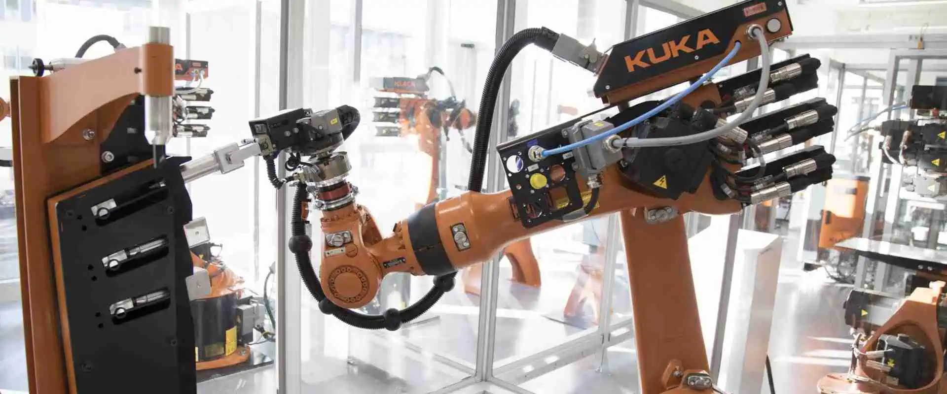
Robots have been around for decades, but their use and complexity have increased drastically over the last few decades. Robots are helpful in various practical applications, from manufacturing to health care. These robots are necessary for assembly line processes, picking and packing, welding, triage, and surveillance. They have many benefits, including being highly reliable and accurate. Military forces even use robots for the same reasons as humans.

YouTube video

An Overview of the Robots Industry

China dominates the Robots industry, but new entrants are entering the market. Moreover, scientists are making new offerings in the collaborative robot market, including plug-and-play cell solutions. These products can be set up faster and at lower costs.

Cost of a complete robot installation

If you’re looking for a complete robot installation, you’ll need to determine how much the cost will be before deciding which type to buy. UR5 robots, for example, cost about 50-100k USD. However, industrial robots could be the right choice if you’re looking for fancier applications. A complete robot installation will need a sturdy pedestal and can handle several thousand pounds of weight.

Cost of a modular robot module

We can determine the cost of a modular robotic module by the number of modules needed. There are a few different modules, such as SEPs, and they share a standard connection interface. Modules can attach and change their polarization. There are few, or many modular robots, and these robots are promising in their versatility and cost. Modular robots come with many benefits, including low-cost production and robustness.

Cost of IoT and cloud systems

Cloud computing and IoT (Internet of Things) platforms have become critical components in robotics development. Google Cloud, Microsoft Azure, and IBM’s Bluemix cloud are among the most popular cloud robotics platforms. Big companies and small start-ups alike are pursuing innovations in this field. Cloud robotics is still in its infancy but will change how industries operate.
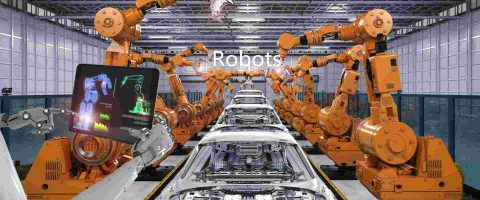
Manufacturing

A new wave of robotics replaces workers in production, distribution, and manufacturing. Machines that can pick up, store, and retrieve goods much faster than human workers are in use in companies like Apple.

The assembly line at Philips, a national grocery distributor, is being run by robots and may eventually replace humans. But, in the meantime, a robot will help make the car you’ve always wanted.

Transportation

Robots are now integral to the transportation industry, significantly impacting every sub-sector. For example, newer robotics systems can adjust operations to consume less energy. In addition, software robots analyze factory data and produce insights into ways to be more environmentally friendly.

As car emissions increase and regulations tighten, this technology will play a pivotal role in the transportation industry. In the coming years, robots will become the norm rather than the exception, and all transportation sub-sectors will depend on different types of robotics.

Home care

The world’s population is aging, with one billion people over 60 expected by 2030. With a predicted 6 million people over 60, one in six people will require the assistance of a nursing professional.

Japanese government subsidies have made it easier for people to use robots. These machines can help lift patients and soothe dementia patients. While we are years away from implementing this technology, it is changing the face of health care.

Future of robotics

Today, we live in a world where robots are advancing rapidly. Robots can assist with physical therapy and surgery, deliver vital supplies, and even mow the lawn. And we have home-based robotic assistants, like Alexa and robot vacuum cleaners.

Robots are also necessary for manufacturing, where they can handle various tasks. For example, robots will help keep us safe by detecting people in our way and triggering an emergency stop.

Moreover, these machines can also help address other mega-trends, societal challenges, and problems. For example, robots can play a crucial role in health and well-being and be life-saving tools during surgeries.

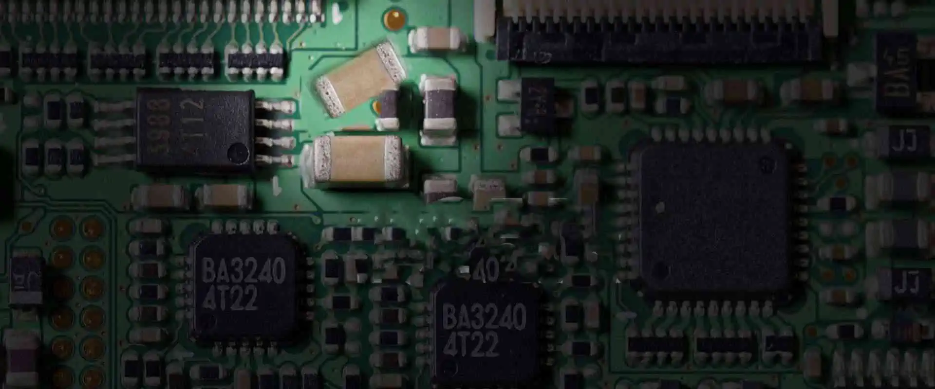
Types of Industrial Robots

Different types of robots can be helpfulย for different kinds of industries. These robots are highly versatile, with different capabilities. Here are some common types of industrial robots. Each type of industrial robot canย perform different tasks. To ensure you get the right robot for your industrial application, it is essential to understand how these robots work.

Historically, industrial robots have been helpful in many different applications. Today, industrial robots focus mainly on data collection and less on their mechanical structure. Older generations of industrial robots had to be completely disconnected from the human workforce to complete their tasks, but modern robots can integrate seamlessly into the workforce.

Types of Robots and Their Different Uses

There are several different industrial robots, and it’s essential to understand how each one functions. Let’s look at delta robots, Cobots, Polar robots, and Articulated robots. What makes them different? Read on to discover what each one does and why it’s essential for your company.

Basic motion application

All five types of industrial robots have similar safety considerations. The typical method for protecting the operators is using an external system to create a fence around the robot. This hard guard can contain a gate or a hard guard that signals the robot to stop moving. Despite these limitations, this type of industrial robot is highly customizable, though its assembly may not be standard among the various types of robots.

Adaptive robotic arms

A six-axis model is the most common industrial robot arm. These robots are highly flexible and offer an impressive list of uses. The six-axis version of the robot has the most versatile capabilities and is, therefore, often the most easily identified type of industrial robot. But, if you’re looking for a more detailed analysis, you can choose from other types of industrial robots.

Cylindrical robots

Cylindrical robots have a cylinder-shaped workspace and are most similar to Cartesian robots. They consist of a rotary shaft, extendable arm, and link-based joint. Cylindrical robots are often helpful for simple applications such as pick-and-place. They are easy to install and often come with complete solutions. These robots are not ideal for many operations, but they can still perform many tasks.

Articulated robots (cartesian robots)

FULL PCB MANUFACTURING Quote

The most common types of industrial robots, articulated robots, can perform complex operations. Typical applications for articulated robots include welding, product assembly, and machining. They have three or more revolute joints on their arm.

Articulated robots can have up to ten joints, with the extra joint enabling more degrees of motion. They can also do more complicated tasks like assembly and arc welding. They are best suited for industrial environments but may be helpful for more complex applications.

The differences between a Cartesian and an Articulated industrial robot are obvious: the former is more flexible than the latter and can perform a wider range of tasks. The joints of Cartesian robots are translational and can move only in straight lines, while an Articulated industrial robot’s joints are rotary and can rotate in any direction.

Nevertheless, both industrial robots are helpful in various settings, including material handling, packaging automation, storage and retrieval, laser cutting, and welding.

However, consider the pros and cons before purchasing Cartesian robots. Articulated robots can lower injury risks and improve employee quality of life. But before purchasing one, consider the costs and the ROI of other automation solutions.

The cost of Cartesian robots depends on their functionality, which we must weigh against the other pros and cons. Its implementation can be costly, especially if the project is complex and requires more programming. Additionally, a dangerous application may require more safety hardware.

Cobot

Cobots and collaborative robots work alongside humans, sharing workspaces with humans. A cobot learns from human motions and can mimic the operator’s movements. However, despite their flexibility, most of the different types of industrial robots have limitations.

For example, these robots are not designed to handle heavy objects or perform tasks with high speed. Therefore, they’re not the best option for high-speed or high-volume tasks.

Cobots, or collaborative robots, can perform various jobs in a factory. They can load machines, perform pick-and-place operations, and move around the facility. They can also perform gluing, drilling, and welding tasks. Some models are suitable for specializing in specific areas of production.

Polar robots

There are several types of polar industrial robots. These are the first industrial robots to be developed. They are also called spherical robots because of their polar coordinate system. Polar robots have two rotary joints and one linear joint, with the arms connected to the rotary base through a twisting joint.

They are helpful for many applications, from material handling to arc and gas welding. They are also known for their gun turret configuration. The most common polar robots are used for manufacturing processes, such as glass handling, material handling, and die casting.

Gantry Robots

Gantry robots can complete many tasks in a manufacturing process. They can be helpfulย for product handling, assembly, and other heavy-duty applications. Because of their long-travel capabilities, they are ideal for applications that require a high payload. They are also great for moving heavy engine blocks or partially finished vehicle assemblies. While other industrial robots can perform similar tasks, gantry robots are superior in many respects.

Scara Robots

If you are a fan of robotics, you have probably heard of Scara robots. These robots are an excellent option for various manufacturing jobs, including welding and other industrial applications. They are also becoming increasingly popular to improve quality control and production. Learn more about them in this article. In addition, here are a few benefits to using them in your manufacturing process. This will help you decide if the Scara robot is right for your business.
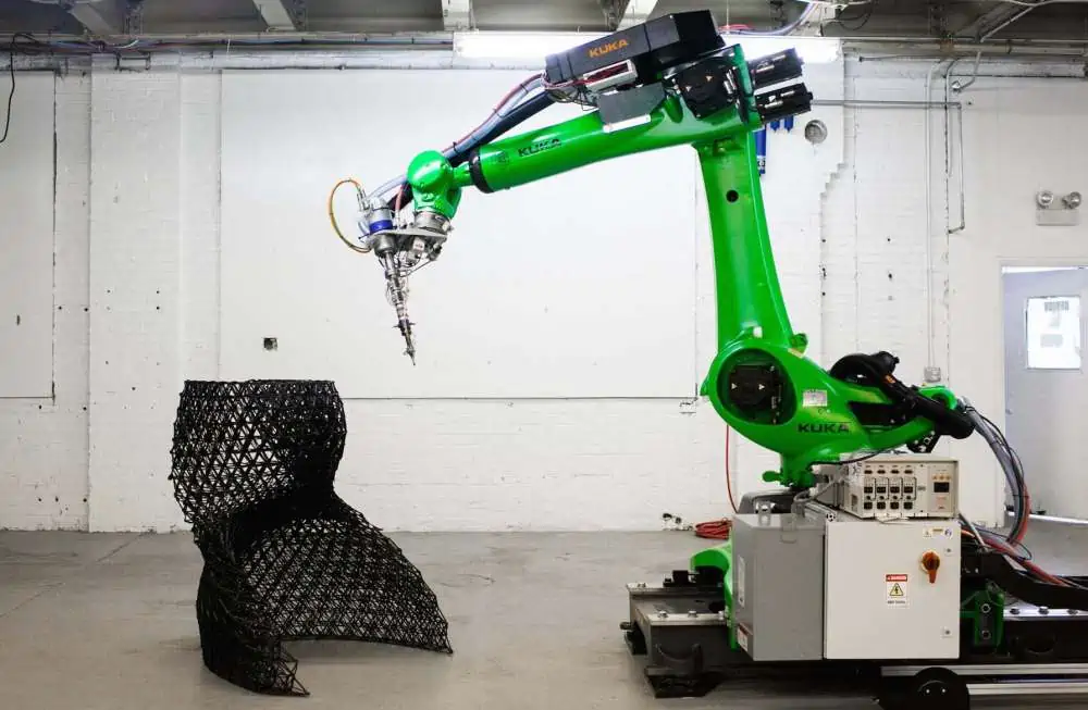
Delta Robots

Delta robots have three arms attached to universal joints at the base. The arms maintain the orientation of the end effector with parallelograms. The end effector sits on a Stewart platform. To change the orientation of the end effector, the robot can rotate the Stewart platform. Here is a video of one such Delta robot in action. The robot can be easily transported from one place to another using the Stewart platform.

Humanoid Robots

While humans have long dreamed of creating intelligent, social robots, humanoid robots are not far away. These robotic machines have the potential to help with plant construction, shipyards, and even maintenance. Many companies are developing humanoids, and the next generation of these machines will have realistic applications. In the meantime, here are some challenges that humanoid robots face. And what about the technology?

How to prevent open defects and tombstones during PCB assembly

PCB Tombstone

PCB Tombstoneing is an art that requires precise knowledge of the components’ placement. This process is most effective if we place the components evenly and with similar orientation and width. If the components are not in the correct position, the copper coverage will be uneven, leading to uneven heating. These mistakes can be avoided during the tombstoning process by following a few essential steps.

YouTube video

Stencil design

PCB Tombstone is a problem caused by the non-uniform thermal conductivity of a PCB. Another cause is poor weldability or oxidation of components. The stencil’s opening or thickness also influences the tombstone. Other factors affecting the quality of the solder paste printing are the printing machine parameters and component placement.

One way to improve the stencil printing process is by making it thinner or thicker. POR stencils have a smaller aperture size than BAE stencils. Both stencils have similar volumes, but BAE stencils are considered better at limiting tombstone defects. Generally speaking, the BAE aperture has better results with 0.4mm prints than POR stencils. However, the BAE aperture is significantly better at limiting tombstone defects with new solder paste.

To avoid tombstoning, you must ensure proper component placement. A good stencil design will prevent this problem by ensuring that the copper pads are evenly covered. Also, the solder mask thickness must be appropriate to avoid oxidation and tombstoning. If it’s too thick, it could cause solder beads.

The stencil design for PCBs is an essential part of the assembly process. Any mistakes here can lead to failure. Therefore, a good stencil design is essential to get consistent printing results. While we can print most PCBs without a complex stencil, certain situations call for a more complex stencil design.

The stencil design also affects solder paste release. The stencil material should be four to eight thou thick to hold solder paste. In addition, the thickness of the stencil should be large enough to allow five solder particles to span the smallest aperture.

Offset printing

FULL PCB MANUFACTURING Quote

PCB Tombstone occurs because of large differences in the wetting force at the solder paste ends of a device. One end of the device may be well soldered while the other is not. The solder paste on the poor end has a lower wetting force than the melted solder paste on the other end. As a result, the solder paste on the poor end has an uneven wetting force. This force imbalance is what causes the tombstone.

Offset printing is another problem, resulting in ineffective solder paste contact. Moreover, the printed-out board will not be complete. This will result in a tombstone that is not fully functional. Fortunately, there are some simple solutions to avoid this issue. The key is to control the paste application process and maintain a proper thermal balance.

There are two main causes of PCB tombstones. First, the pads do not have the proper design. As a result, they often do not cover more than 50% of the component’s terminals. In addition, the spaces between the pads are too wide. When these problems occur, reflow soldering can create a tombstone.

Second, before the soldering process begins, you must preheat the board’s surface. A significant temperature difference at the end of the board could lead to the formation of tin beads, which could make the PCB look like a tombstone. A reflow soldering process with a controlled temperature profile will reduce tombstones.

Another problem associated with tombstoning is the wetting force. The wetting force at one end is much greater than the combined force of the two ends. The result is that one end of the component will rise, and the other will fall. To avoid this problem, choose smaller and lighter-weight components.

Uneven wetting force

PCB Tombstone is a type of PCB defect resulting from uneven solder wetting force. The uneven wetting force is because of significant differences in solder paste temperature between two ends of the device. This makes solder paste on one end melt while it does not melt on the other. As a result, the tombstone’s wetting force is lower than that of the other end.

The most common cause of tombstones is an imbalance in the wetting force of two terminals. The force generated at one end of the component is greater than the combined force from the two ends, causing the component to rise out of the solder. This is particularly problematic in smaller and lighter-weight components.

Another common cause of tombstone is the non-uniform thermal conductivity of the PCB. This condition may result from improper solder application or insufficient solder paste thickness. Therefore, solder paste printing machines should also calibrate to ensure uniform thickness.

Uneven wetting force of PCB Tombstone is a common problem when reflowing the solder on components. This uneven wetting force causes the component to stand up on one end and overpowers the other. It is often the case when the components are small and located in a small package. A proper balance of the wetting force between the two ends can prevent this problem.

Uneven wetting force of PCB Tombstone can reduce by adjusting the pad size. A larger pad size increases the surface area of the molten solder, which causes a stronger wetting force on the component’s end. This also reduces the likelihood of component separation. The IPC standard provides recommendations for pad sizes. However, pad sizes vary from manufacturer to manufacturer.

Manhattan effect

The PCB Tombstone defect, also known as the Manhattan effect or the Stonehenge effect, is serious in surface mount devices. It is due to an imbalanced wetting force and can cause an open circuit. This issue often occurs when the solder paste on one end of a device is much hotter than the other. This causes a significant force imbalance and results in a tombstone.

One important factor in preventing tombstoning is component placement. When the component is small, it is essential to place it evenly across the pads. In addition, the traces must be of the same width and orientation. If they are unequal, the solder will not reach the component. This problem is common in low-cost, low-margin products but can also occur on high-margin devices.

Another factor affecting PCB Tombstone is uneven wetting force. During PCB reflow soldering, uneven wetting forces can cause the chip component to stand up. This condition is known as the Manhattan effect. Improving process design, quality control, process modulation, and straight-through assembly rate can reduce it. Good solderability of the solder paste is also essential. It is possible to control solder end size error, but this is more sensitive to the size of the PCB pad.

An imbalance causes the Manhattan effect in solder paste applied to the two sides of a PCB. When this happens, the solder paste on one end of a device may melt before the other. As a result, it pulls the part to the melted side. The Manhattan effect, also known as the drawbridge effect, can cause the tombstone effect.

Soldering rework

Tombstone is a soldering defect resulting in partially or fully lifted passive SMT components from the PCB pad. It typically occurs when one end of a chip is soldered to a PCB pad while the other end is not. As a result, the component’s terminals are not fully covered by the solder paste, resulting in uneven heating.

This defect can result in intermittent electrical issues. Fortunately, you can repair it by turning it into a pillow defect. First, remove the component from its attached pad. Then, place it on the board’s other side and apply flux. After applying flux to the component, heat the first side of the board.

A hot air rework station includes a wand holder and a reflow station. A polarized component is placed backward, shifted x degrees to one side, or has an unintended solder jumper. This component is easier to replace when placed before the reflow process. A second common issue is a component that is missing. This can happen during the reflow process or before it occurs. In the case of a missing component, hot air can help replace it.

Robotic 3D printing – How to Select the Right 3D Printer

robotic 3d printing

When selecting a 3D printer, there are several factors to consider, including price, the quality of prints, the cameras, system software, and of course, your specific needs. We’ve discussed these factors in detail to make your decision easier. Read on for more information. After you’ve decided on the printer, you’ll need to decide what type of printing you’d like to do.

The Rise of Robotics – The Rise of Machines With 3D Printing

In the 20th century, most robots were essential in assembly tasks, mainly mechanical arms that could weld car parts. Now, humanoid robots can serve as doormen and even bring you coffee. While the development of these robots has only recently been entirely in use, the idea of robots has been around for a long time. The first descriptions of robots date back to the time of Heron of Alexandria, who described over 100 machines.

The rise of robotics has a huge potential in manufacturing. Although the market for 3D printing robots is still in its infancy, several industry research efforts have already recognized the value of this emerging technology. This technology enables manufacturers to create 3D objects using various materials. This opens new possibilities for smart additive manufacturing in the future. Automation is one of the significant advantages of 3D printing robots.

A French start-up, XtreeE, is working on this technology. An ABB robotic arm with a concrete extruder can produce complex geometric structures up to 14 meters tall. The flexibility of this robot allows designers to experiment with different shapes and movements. The company has an impressive project portfolio, including 3D-printed facade panels and benches. The company is also working on developing 3D-printed facade panels and pavilions.

Industrial robot arms can be equipped with several degrees of freedom, allowing them to move freely in all directions. They also can reorient print paths as needed. Robots can also have OCTOPUZ software, which enables the robots to move in multiple directions. Further, robot additive systems can print in infinite directions. This technology is not just a novelty but will become a significant part of additive manufacturing.

4 Ways Robots and 3D Printing Intersect

3d printing

The intersection of robotic automation and additive manufacturing is powerful and will revolutionize many business areas. One example is the integration of six 3D printers with a collaborative robot, which can remove build plates containing finished parts and start a new cycle. This integration was a creative challenge, but the result is a fully automated cell that runs 24 hours a day. Here are four ways robots and 3D printing intersect:

Swarmscapers

Autonomous robots are already transforming the way we build and use our world. For example, a California College of Arts professor has developed autonomous robots called Swarmscapers, which harness materials native to the site. As part of his master’s program in the Digital Crafts Lab, Swarmscapers navigate a chamber filled with sawdust. They then use a glue extruder to bind layers of sawdust together to form ovular cone clusters resembling termite mounds.

In April 2015, a massive earthquake devastated central Nepal, leaving villagers homeless and thousands dead. Field Ready’s team noticed a life-threatening problem in one of the camps. A leaky pipe was a possible entry point for disease. They had a 3D printer mounted to a pickup truck to address the issue. This allowed them to create a pipe fitting on the spot – and the pipe fitting still holds a few months later.

Scaling up of 3D printing processes

Robotic arms have enabled the scaling up of 3D printing processes while also enabling the realization of nonplanar path geometries. These properties make 3D printing viable for many architectural applications, although the challenges associated with nonplanar layered paths prevent widespread use and integration into design processes. The methods presented here contribute to developing flexible nonplanar layered paths for robotic printing. It’s an exciting time for the world of robotics.

In a few years, robotic systems will be the norm in manufacturing. Large machinery will be the exception. Companies that can afford the cost and complexity of this technology will likely become the sole users of robotic 3D printing. By 2080, half of the world will be using robotic-based manufacturing lines. If this trend continues, robotics will make additive manufacturing easier for businesses of all sizes. It’s a game-changing development for the entire industry.

Integration with large scale objects

While 3D printers will soon replace workers on construction sites, they will still be necessary for constructing physical objects. Many robots and 3D printers are proving their utility in building large-scale objects.

Robots attached to drones are already proving their versatility and cost-saving abilities. This is one of the first applications for robotics in the real world. While these innovations are not yet available in a production environment, the potential for automation and robotics is immense.

Innovative customization

As a growing field, 3D printers will also help develop medical implants. We can customize these 3D-printed parts according to the specifications of the patient. Innovative scientists are already studying the possibilities of 3D-printed tissue and organs. Despite these applications, 3D printers will still require human workers. In addition, 3D-printed prosthetics will be cheaper and more comfortable for the patients.

Benefits of Robotic Arm 3D Printing Platforms and Software

FULL PCB MANUFACTURING Quote

If you are a robotics maker, you are likely considering the benefits of a Robotic Arm 3D Printing Platform and Software. You should consider several factors, including cost, functionality, and availability.

The robot arm design, for example, may be ideal for the hobbyist, but it could also be useful in the professional field. Here are some of the benefits of this type of software.

Precision

The robot arm’s high level of precision is essential for the success of wireframe structures. The designer can move the robotic arm from one position to another without worrying about its stability.

However, this can lead to fine filament strands. Fortunately, these strands do not diminish the functionality of the printed model. This makes robotic arms a more flexible and affordable option. They can also print larger objects.

Virtual control

RoMA combines a virtual reality headset, controllers, and a 6DOF robotic arm. The system has a high-resolution camera for viewing images and lets the designer control the arm through a virtual interface. As a result, the designer can step away from the printing platform and continue designing. After the design is complete, the robotic fabricator controls the platform. This is a revolutionary solution for any 3D printer.

Multiple printing

Another feature of robotic arms is their ability to print on various substrates. With the right software, they can print at virtually any angle and with different mounting options. As a result, they are ideal for repairs of large objects and can be helpful in hybrid manufacturing where we can add a printed section to a cast, forged, or machined part. Viridis3D specifically designed its RAM 123 printer for foundry applications.

Modeling experience

RoMA also provides a hands-on modeling experience. The designer creates their model with an AR CAD editor, and the robotic arm builds the features concurrently. A partially printed physical model serves as a reference for the designer.

This tool also integrates real-world constraints into the design process by allowing the designer to design directly on the physical object. These advantages make RoMA the ideal 3D Printing Platform for architects, industrial designers, and hobbyists.

The robotic arm 3D printer requires more detailed computer instructions to print the part. In addition, because the robotic arm can reach around the printed part at multiple angles, the multi-axis toolpath must consider this to prevent collisions with the part.

Robotic Arm 3D Printing Platforms & Software are a must for any professional or hobbyist. If you are considering using this technology, don’t hesitate to read on to learn more about the pros and cons of using robotic arms in 3D printing.

Can handle complex projects

Soft robots consist of viscoelastic hydrogels, which can handle high pressure and complex geometries and shapes. The research on the materials and 3D printing techniques is intensive, with researchers in the Netherlands developing UltiCast, a technique that allows you to create a soft-grip. The UltiCast method has the advantage of being simple to replicate and inexpensive to implement.

3D Printed Off-Robot Accessories

Many companies have begun producing 3D printed off-Robot accessories. These accessories are often more durable and can be helpful for various robot applications. You can also use several different materials to 3D print these accessories.

For example, you can use PETG filament to print accessories such as a hook for your robot. However, it is essential to use PETG carefully as it can warp when printing.

When designing the accessories for your robot, consider what you need. For example, if you want the robot arm to work underwater, you might need torch holders or grippers for its front legs. 3D printed accessories can be made of various materials and are available in many shapes and sizes.

So whether your robot arm is ideal near the surface or deep in the ocean, you can design a custom accessory. It might be something as simple as a torch or something more complicated, like a flashlight.

To make the most of your 3D printed off-Robot accessory, you should place it on the opposite side of the mold as the part it is intended to serve. That way, you won’t end up with an awkward and costly assembly.

Additionally, 3D printed accessories are not only helpful but also cost-effective. These accessories are an essential part of the entire robotic system. A polymer printer is an excellent option for this project.

AM Flexbot Integrated Robot System

The AM Flexbot is an integrated robotics system that can be helpful for various applications. Its innovative structure comprises aluminum profiles and has fixings to break the mechanical bond during manufacturing.

opening door and locking mechanism

The AM Flexbot integrated robot system features include a three-hundred millimeter opening door and locking mechanism. In addition, it offers an ISO 13857 and ISO 14120 certified safety cage. As a result, its integrated robot system satisfies all safety standards.

Pellet extruder robot arm

The AM Flexbot pellet extruder robot arm is ideal for seamless integration with the robotic arm. It is lightweight and has a temperature range of 400degC. It can process nearly any thermoplastic, engineering-grade material, including materials with carbon fiber fillers. AM Flexbot pellet extruder robot can process ABS CF, PESU CF, PP GF, PPS CF, and PU-CF.

Comau NJ60-2.2 six-axis robotic arm

AM Flexbot comes equipped with a Comau NJ60-2.2 six-axis robotic arm, which can lift a payload of 60 kg. In addition, the system has a Siemens Sinumerik 840D controller, which enables the user to customize its control settings and move the robotic arm precisely. This controller is also a standard for 5-axis milling equipment. For complete customization, AM Flexbot can help in many applications.

Flexibility

The Flex-Bot can handle various tasks, from mechanical engineering to electronic assembly. It is ideal for medical device handling, kitting, palletization, and tray loading. It can handle parts of various sizes, and its modularity makes it easy to integrate with AS/RS and other palletizers. In addition, its modular design and advanced safety features make it an excellent option for a wide variety of applications.

Interlocking modules

The core frame of the FLX BOT is composed of half a dozen interlocking modules. With a diameter of one inch, it can easily enter difficult-to-reach spaces. Several end effectors are interchangeable, including a drill, a gripper, a vacuum, a soldering iron, or a block grabber. Block grabbers can fetch up to $100+ depending on length.

The research plan includes developing test methods and metrics that assess the robot’s agility. This information will help companies improve their robots’ performance, collaborate more effectively with other robotic systems, and enhance assembly-centric manufacturing.

The AM Flexbot is a groundbreaking system for industrial automation. Its performance measures will increase productivity and efficiency while decreasing cost. The robot will also be able to reconfigure itself to meet changing assembly demands.

The Large Scale Additive Manufacturing Process

Large scale additive manufacturing process is a process that can manufacture large, complex parts very quickly and efficiently. It is suitable for industrial use, reducing the need for pre-fabricated parts and third-party tools. A 3D-printed metal part can reduce raw material consumption by up to 80% while maintaining structural integrity.

For the future of on-orbit manufacturing, additive manufacturing is essential. However, current state-of-the-art on-orbit manufacturing systems face limitations from launch constraints and thus reduce the building volume.

Large-scale additive manufacturing can remove these constraints and allow the construction of more complex structures. But how can this type of technology be applied to spacecraft manufacturing?

In industrial applications, large-scale additive manufacturing systems are ideal for rapid prototyping. They can produce parts with a net or near-net shapes. They’re also suitable for aerospace, automotive, and defense applications.

Several industries have begun to manufacture the technology, driven by the increased build volume and speed of new 3D printers. For example, Airtech has already incorporated the technology into additive manufacturing systems for large prototypes. In addition to manufacturing parts in virgin thermoplastics, they can also produce electronic components.

A large-scale additive manufacturing process can also help make parts of various materials, such as titanium, stainless steel, and aluminum. These materials can be used in aerospace applications and may ultimately replace the need for large-scale casting and forging.

However, they have some limitations, such as poor durability. In addition, high-heat applications may require a specialized method to join different types of materials. We can overcome these limitations by using thermoset composite materials.

What are the Best Automotive PCB Manufacturers?

Automotive PCB Manufacturers

Automotive PCB manufacturers and suppliers are doing all they can to produce standard PCBs that ensure the efficiency of all the systems. In addition, the modern standards of the automotive industry include advanced technology. This is one reason why there are lots of questions regarding automotive PCB manufacturers in your mind.

Due to the number of automotive PCB manufacturers in the market, we have done some research and come up with some of the very best. Before that, letโ€™s briefly talk about what an automotive PCB is.

What is an Automotive PCB?

Automotive Car PCB

An automotive PCB is a complex circuit system that can control most of the electronic operations of a car. What this means is that, when using automotive PCBs, you must ensure that it is extremely durable, very reliable, and you can get it at very competitive rates.

This is why it is very important that you work with the best automotive PCB manufacturers

8 Best Automotive PCB Manufacturers

Here are some of the best Automotive PCB manufacturers in different locations across the globe.

PCBANow

This is one of the automotive PCB manufacturers with about 15 years of professional experience. They also specialize in the ic design as well as manufacturing of PCBA. The products they manufacture are used widely in automotive electronics, industrial automation, smart appliances, consumer electronics, security products, RF equipment, IoT equipment, as well as other industries.

PCBANow is known all over the world and has gained the trust of over 2000 customers both abroad and home. With the high quality service, the company avoids unnecessary costs which is caused due to quality issues and helps in saving you some precious time.

RLX Solutions Inc.

RLX Solutions Inc. is a Canadian company and functions as a distributor and manufacturer. This company produces different mechanical/electronic equipment from printed circuit boards, custom mechanical components, and custom cable manufacturing.

With international representation, RLX Solutions Inc stands by their quick-turn and reliable solutions for the production and design. RLX is known as the authorized reseller and distributor for a number of semiconductor and passive components, as well as LED brands. This automotive PCB manufacturer actively offers its services in Canada and also has a very strong sales and manufacturing presence internationally in more than 100 countries.

Rayming PCB & Assembly

FULL PCB MANUFACTURING Quote

Rayming PCB & Assembly is also ranked among the best automotive PCB manufacturers. They are world leaders when it comes to the manufacturing as well as assembly of printed circuit boards. Established since 2005, the company is involved in offering companies of different sizes all over the world with components sourcing, PCB assembly, and PCB fabrication.

Also, Rayming PCB & Assembly offers its services in high end boards like Teflon PCB, Rogers PCB. HDI boards and more. Also, this company has created a reliable team that ensures you get the very best automotive PCB. They are skilled in every aspect regarding PCB Assembly and custom manufacturing.

Rush PCB

Rush PCB is also ranked among the best automotive PCB manufacturers. Since 1997, this company has been actively involved in the serving of the electronics industry with the assembly services and printed circuit boards all over the U.S and around the globe.

Rush PCB majorly focuses on the manufacturing of 2 โ€“ 32 layers circuit boards. They also offer complete turn-key assemblies as well as quick-turn consigned assemblies. Their services include PCB assembly, PCB design, PCB fabrication, and PCB manufacturing.

Andus Electronic

Andus Electronic was founded back in 1969, as is well-known among the top automotive PCB manufacturers.  This company is also involved in the production of printed circuit boards of high quality. They specialize in prototypes, as well as orders with small and medium sizes.

As of today, the company has more than 50 employees that are qualified. Their CAM-team is also involved in inspecting and optimizing all the files in an intensive way before it goes in for production.

In addition, their technology consultant as well as sales team helps in the preparation of quotations and answers that are easy to read. Also, with their private production facility situated in Germany, this company can deliver high quality, unrivaled speed, as well as professional service. Here, electronic developers will be able to find system solutions as well as lots of innovative technologies for printed circuit boards.

3CEMS

3CEMS is also included among the top automotive PCB manufacturers. This is supported by over 25 years of professional experience globally. This company keeps driving to be one of the top suppliers of the EMS industry.

3 CEMS virtually integrates the capabilities of their factories, supply chain and know-how management so as to meet even strict requirements of customers. This company offers customers a complete solution including PCBA, PCB, system integration/build and different join design services.

Agile Circuit

Agile Circuit is one of the top automotive pcb manufacturers specializing in offering solutions for different custom circuit boards. Also, they offer services of high efficiency at very competitive prices.

This company also supplies PCB boards for different applications, like consumer electronics, telecommunication, and aerospace. It also serves industrial control, automotive, military, medical as well as other top assembly industries.

This automotive PCB manufacturer started its operations in 2003, and has grown to offer different services to customers. These include PCB assembly, mass production of PCB, PCB prototypes, etc. The goal of this company is to be the best and reliable partner to customers. This they achieve by offering help in the design as well as completion of the PCB.

Bay Area Circuits

Since 1975, this is one of the best automotive manufacturers that has been involved in meeting the needs of PCB manufacturing. They offer services for high technological contract assemblers, electronics manufacturers, and the design engineers. The companyโ€™s manufacturing process includes the design, the fabrication, as well as assembly. Also, it offers the best solutions for all projects. This makes sure that there is complete quality and value for customers.

Conclusion

Hope we have been able to review some of the best automotive PCB manufacturers in different areas across the globe. You can do your own research to have more options in your location.

How to Use Altium Multi Board PCB Designer

Altium Designer 20

It can be much easier to create a multi board system when you integrate the best PCB software for your PCB. Some electronic devices feature multi board systems connected with cables. In those days, PCB design software handled each board in the system separately without the need to consider crucial circuit board design challenges such as high-speed routing, power distribution, and mechanical assembly.

YouTube video

Furthermore, PCB design software has met the demands of circuit board designers. However, you need to choose the appropriate PCB design package to design your multi board system. With Altium multi board designer, you can have access to design tools for creating a multi board system.

How to Plan Your Multi Board System Design

Multi board design usually begins with a physical outline of every board in your system. Therefore, it is important to plan how to connect this board to each other. The connection method could also involve standardized connectors like pin headers. Also, the multi board design process usually starts with schematic capture and then transforms to a complete PCB layout for every board. This process ends with a documentation package.

Multi board PCB arrangement involves specifying connections between all PCBs in the system.

Determine the board arrangement

You will need to determine how you will arrange the boards. Also, you will need to start mechanical modeling and determine the design.

Select connectors

You need to choose connectors to support the board arrangement while fitting in your enclosure.

Decide the functions of the board

A multi board system comprises several circuits with each performing certain functions. Also, these boards will only hold the require components that support this function. Therefore, you might need to reconsider your circuit board arrangement as well as the connector options

Identify signals across connectors

Every connector must support certain groups of signals and also ensure the design has signal integrity. Furthermore, you can determine the pinouts in this stage and define them on schematic symbols.

Create schematics

It is advisable to segment schematics. This will help to reflect your board arrangement in your multi board system. Also, every set of schematics should comprise components from a single board. Avoid placing components from different PCBs in the same schematic sheets.

Native 3D Board Design for Altium Multi Board Assemblies

Some modeling and measurements are complex in 2D. Therefore, this creates interference risk between your PCB and components. A multi board assembly involves multiple circuits and as such, unwanted interference could come up between boards in the design. Also, unwanted interference would occur between cables, components, and other elements.

Integrating a mechanical backchecking in the design process is a great way to prevent any interferences. Backchecking involves automatically checking clearances by using MCAD tools. These tools examine the 3D model of your PCB, components, and enclosure. The design software can develop a realistic model by simply combining the STEP models for every component in your PCB design.

A mechanical designer can help you generate a model of the circuit board enclosure if you work with one. You can  then import this model in your PCB designer to execute interference checking in the ECAD tools. Alternatively, you can export an IDF file or STEP model for the circuit board. You can then import this model or file into an MCAD for backchecking.

You can route the design after you have completed the initial placement and checked for interferences. Also, multi-board systems demand some critical routing considerations.

How to Route and Define Ground in Multi Board System

FULL PCB MANUFACTURING Quote

You should perform routing after creating initial design rules, creating the design in the right routing mode, and calculating the needed impedance profile. Although high speed interfaces arenโ€™t available in every board, you can route between circuit boards in a multi board design via a board-to-board connector.

Also, you can route single-ended signals between boards and over cables. But, you must ensure uniform grounding to avoid signal integrity issues that may occur. Grounds need to be well defined in multi board layout. This will enable routability for signals. Ensure you follow this process when you are routing signal paths between circuit boards.

  • Integrate ground planes in every board to offer characteristic impedance. Therefore, this provides protection to suppress crosstalk or EMI.
  • Add a ground connection across connectors when routing between two PCBs. This will help to connect the ground regions in every circuit board.
  • Integrate interleaved ground between signals. This offers a stronger protection and clear reference in the routing path.

It is crucial to use ground when you are routing across a connection between PCB designs in a multi board system. Also, this helps to specify crosstalk suppression and return paths in multi board design and routing.

Why Altium Multi Board Designer is Easy to Use

Altium multi board design system integrates a 64-bit architecture. Therefore, this makes Altium capable of handling any challenge. Also, the intuitive interface helps first-time users to find their way around this multi board design. Also, Altium is one of the best and most versatile schematic capture software applications in the world today.

Altium multi board designer is specially created to handle very complex multi board designs. Also, Altium designer feature multi board design capabilities. Altium multi board designer is easy to use as it allows users to import their design into MCAD applications for modeling. Furthermore, Altium multi board designer supports the transfer process from ECAD to MCAD.

Also, the relationship between ECAD and MCAD makes it easy to place densely packed components. Furthermore, there is a multi board assembly editor that displays how the circuit boards plug into one another.  Altium multi board designer has a unified environment that includes all design tools in a program.

Furthermore, Altium offers a multichannel schematic editor for multi board PCB design. With Altium, the schematic capture is quite easy as you donโ€™t need a different program for PCB layout.

Conclusion

Altium multi board designer gives you access to all the aspects of multi board design. With this designer, you can take full control over your multi board design. Altium designer offers more than you can ever imagine. Do well to explore the Altium multi board designer today.

Why Wireless PCB Assembly is Crucial in Some Electronic Devices

Wireless PCB assembly

Printed circuit boards are a crucial part of electronic devices. They serve as the backbone of these devices as they provide physical and electrical connections among electronic components. They are different kinds of printed circuit boards and a wireless PCB is one of them. Also, a wireless circuit board is commonly found in smartphones and other wireless devices. In this article, we will be focusing majorly on wireless PCB assembly.

YouTube video

What is a Wireless PCB?

A wireless PCB is a very thin circuit board that comprises composite epoxy, copper, fiberglass, and some laminated materials. A circuit board integrates conductive pads and tracks to offer electrical connection and mechanical support to electronic devices. Bluetooth is wireless communication technology. Also, this wireless technology integrates wireless signal to transmit data among electronic devices. However, this wireless technology can only cover a short distance.

Furthermore, Bluetooth devices donโ€™t need wires to enable connection. So, what is a wireless circuit board? A wireless circuit board integrates wireless technology and offers connection over devices. Also, this circuit integrates Bluetooth technology. Devices that integrate wireless PCBs include wireless speakers, computers, and mobile phones among others.

Wireless circuit boards feature an antenna that receives signal transmitted by another Bluetooth device. After processing the signals in the circuit, the message transmits to the output devices.  The designing of a wireless circuit entails the integration of some vital components. Furthermore, a wireless PCB assembly comprises at least two inductors. These inductors fine-tune the power of the antenna to transmit and receive signals.

Also, the PCB module comprises four I/O pins i.e. Input/output pins. These pins are the power supply option, enabled, communication, and the state.

Wireless PCB Assembly Process

Wifi PCB Module
Wifi PCB Module

Wireless PCB assembly process involves several steps. Also, this process usually begins with drawing a schematic diagram of the PCB. After you have created the schematic diagram, you can now place the necessary electronic components on the bare wireless board. The major step in this process is the mounting of electronic components.

A wireless PCB assembly is a circuit that comprises already installed electronic components. Also, you will need to choose the layer for your PCB. The PCB assembly process is the most crucial process in wireless PCB manufacturing.

You will need to place all components by simply following the line in the schematic diagram. To achieve a successful PCB assembly, you need to integrate the right schematic diagram. Soldering is an important step in wireless PCB assembly. This step requires extra attention and care. Also, overheating can damage the circuit board and other components. Furthermore, donโ€™t place vital components beside the boardโ€™s heating part. Also, the soldering part is very important. Placing the right components makes the next step easier.

Therefore, ensure you place the appropriate components in the appropriate place. Solder the components and use the melting solder to permanently connect the component in the boards. The assembly process involves the use of automated soldering.

After a successful wireless PCB assembly, ensure the board passes through quality control. Makes sure you integrate the right inspection and testing method. After this, your wireless circuit board is ready to perform its best.

Applications of Wireless PCB Assembly

In the world today, there are several devices that integrate wireless PCBAs.

Wireless earphone

A wireless earphone is usually Bluetooth-enabled. Therefore, this gadget comprises a wireless circuit. Without a wireless PCB, this device canโ€™t function.

Computing devices

Wireless PCBAs are commonly found in computer parts like wireless mouse and keyboard. Also, these computer parts are Bluetooth-enabled i.e they connect to the Bluetooth of a computer to function.

Wireless communication devices

Wireless communication devices such as cell phones, G{S units, and satellite television comprise wireless PCB assembly. Also, a wireless communication system helps to locate and track, access the internet, abd also enhance security.

Wireless medical devices

Wireless PCBAs are commonly found in some medical devices. Examples of these devices include glucose monitors and pacemakers. Also, these devices execute at least one function that integrates wireless RF communication like Bluetooth or Wi-Fi.

What are the Main Wireless PCB Protocols?

FULL PCB MANUFACTURING Quote

 Wireless solution technology comprises four main protocols which are:

Bluetooth radio and baseband

Bluetooth radio integrates radio signal specification. This signal offers compatibility with the 2.4 GHz ISM band.

Antenna/RF component

RF and Antenna require special attentions since they carry out one of the primary tasks in a wireless board. Also, the antenna design with this circuit board is complex. There is an in-built antenna in the PCB design. This antenna needs a special design.

Bluetooth application protocol

This protocol comprises application profiles that enable wireless PCB users to link the devices utilizing the radio signals.

Wireless software protocol stack

This is the driver code. It enables the Bluetooth-powered device to receive and transmit signals from yje Bluetooth module in them.

Advantages and Disadvantages of Wireless PCB Technology

Wireless PCB technology offers a lot of advantages in the electronics industry. However, this technology has its own disadvantages.

Advantages

  • It prevents interference from some other wireless devices
  • Very cost-effective
  • It requires no wire or cable
  • Ideal for data transfer or wireless voice
  • Offers easy upgrade benefits
  • Low power consumption
  • It has higher range than infrared devices

Disadvantages

  • It features low bandwidth
  • The connection might get lost due to some conditions
  • Low security

What to Consider in Wireless PCB Assembly

There are several factors to consider during a wireless PCB assembly. The performance of a wireless PCB is directly related to its assembly. Here are some factors to consider before assembling a wireless PCB.

  • Ensure all the tools are available
  • Separate signal and sensitive components
  • Utilize a certified Bluetooth module

This might be costly; however, it will save some time and enhance the development process. Also, it offers solutions to antenna placement issue.

  • Ensure the right components are used

Conclusion

Wireless PCB technology provides solutions to certain problems in the electronics industry. Therefore, the drawbacks of this PCB arenโ€™t as evident as its benefits. We have discussed the applications and benefits of this PCB in this article.

Benefits and Applications of Soft PCB in Electronics Manufacturing

flexible printed circuit

Printed circuit boards are mostly found in electronic devices as they serve several functions. They serve as the backbone of electronic devices. There are several types of circuit boards based on their ability to bend. These circuit boards are rigid and soft boards. We will focus on soft PCBs in this article.

What is a Soft PCB?

A soft PCB is also known as a flexible printed circuit board. It is a circuit board that can bend, fold, or twist into any shape. This circuit board is a good invention in the electronics industry as it serves several purposes. A soft PCB is very lightweight and flexible. However, the processing of this circuit board requires further protocols like material handling, special clamping, and more.

Soft PCBs are often used in wearable devices as they can stick to the body easily. These PCBs arenโ€™t simple or cheap to produce. Hence, they are usually designed by companies that need them. The materials used for this PCB must not be too flexible so that it breaks the board when twisted or bent.

Before the advent of soft boards, electronic producers incorporated rigid boards. In few products like wrist watch, there was less space for rigid boards. However, there was a need for flexible circuit boards in some devices. Therefore, soft circuit boards came into existence.

Also, soft PCBs have made it possible to produce hand-carry electronic products like flexible keyboard. You can easily roll and put this keyboard in your bag. Furthermore, flexible circuits have a great impact in oil & gas sector. These boards have the ability to withstand high temperatures.

Soft PCB manufacturing process involves steps that are similar to that of multilayer PCB. Also, soft boards are usually designed from a thin insulating polymer film. The applications of these boards keep growing every day. Also, soft PCBs can be single sided, double sided, and multilayer.

Materials used in Soft PCB

There are some basic materials used in the production of soft circuit boards. These materials are essential for the performance of a soft PCB.

Insulators

Insulators separate electrical conductors. These materials fail to conduct current themselves. Also, they serve as support to other components in the circuit. Examples of insulators include solder mask, polyimide, and polyethylene naphthalene.

Conductors

Conductors enable the free flow of electrical current. The most commonly used material for conductor is copper. This is because copper is a highly conductive material. However, other materials used for conductors include, silver, carbon, aluminum.

Adhesives

Adhesives serve as a binding for surface mount components. Also, the uses of adhesives depend on the thickness of conductor and customer requirements. Examples of adhesives include acrylic and epoxy. Some soft PCBs donโ€™t require many adhesives.

Finishes

Finishes serve as protection. They protect the metal surface against oxidation. Also, the application of the circuit board determines the final finish. There are several types of finishes you can use. These include immersion gold or silver, tin, palladium gold.

Benefits of Soft PCB

Soft PCBs offer a lot of benefits. These circuit boards arenโ€™t just flexible; they have got good features which make them relevant in the electronics industry.

Light weight

Soft PCBs are light weight. These PCBs are usually created from plastic or epoxy. Also, soft circuit boards donโ€™t feature substrate core. Their small weight is a result of the SMD components available in them. Also, soft PCBs comprise the thinnest substrate materials.

Small size

One of the greatest advantages of a soft PCB is its size. Therefore, this circuit board can fit into a small space. It can be simply adjusted in small spaces. Also, it has negligible width just like paper.

Resistance to high temperature

Soft PCBs can resist high temperatures and as such, are ideal for use in oil and gas sector. In oil and gas sector, rigid boards can easily melt out. The ability of these PCBs to withstand temperature depends on the material used for their fabrication.

Improved capability

People often believe that soft PCBs donโ€™t usually have great capability like rigid boards since they are just flexible. Soft circuit boards have great capability as they improve the general performance of electronic devices by enhancing component density.  

High durability

Soft PCBs can stand the test of time if treated well. These boards are very durable since their manufacturing takes place under precise conditions. Also, these boards are usually coated with formulated materials.

Reliability

Soft PCBs integrate less mechanical connectors. Also, there is a minimal use of interconnection points. Therefore, the system proves to be more reliable. Furthermore, this PCB enables increased heat dissipation.

Applications of Soft PCB

FULL PCB MANUFACTURING Quote

Soft PCBs are specifically used in some applications. They are not as common as rigid PCBs, but they have found their way in some applications.

Wearables

Soft PCBs are commonly used in wearable devices like spy microphones, wrist watches, smart cameras, and more. These circuit boards have proved to be very useful in the production of wearable devices.

Printers

Print-heat of printers integrates soft PCBs that offer a pathway to link signal with the arm of the disk drive.

Consumer electronics

Soft PCBs are ideal for use in consumer electronics like cameras, calculators, entertainment devices.

Medical devices

These PCBs are ideal for producing some medical devices.  There are several wearable devices in the medical field. For instance, soft PCBs are available in heart monitor devices, body-mounted sensors, and fitness trackers. Patients can wear these devices to regulate and monitor some issues in their body.

Industry

Soft PCBs are ideal for use in the production of robotic arms, bar code equipment, processing machines, and more. Some industrial devices feature soft boards.

The use of soft PCBs keeps growing across various sectors. These PCBs is ideal for use in main electronic sectors like wearables, consumer, electro-medical devices, and automotive.

Conclusion

There are several electronic devices that use soft PCBs. These devices include computer keyboards, consumer electronics, and wearable devices. Soft circuit boards were majorly introduced to utilize the flexible areas of a product. Due to their flexibility and lightweight, the production equipment used for fabricating these boards can be light.

What is Polaris PCB?

Doosan Middle Tg DS-7402 PCB

Polari is known as an innovative company that offers electronic contract manufacturing services in China. It was established back in 2009.

The main services that Polaris pcb offers include PCB assembly and pcb manufacturing, cable assembly, wiring harness, stencils, full turnkey manufacturing solutions, metal and plastic solutions, etc.

Polaris PCB is also dedicated to serving the companies with good service and high-quality products. This has assisted Polaris PCB to win over 2000 customers globally in different sectors including the Industrial, Medical, Communications, Automobile, Aerospace, and emerging electronic products

To meet the different demands of the customer, Polaris PCB has set up different parts for PCB. One serves the medium and small quantity service, while the other offers volume production. The PCB factory of Polaris PCB has a total area of over 30000 square meters. Also, Polaris PCB has about 700 workers, and the rate of their technical staff is over 35%.

Furthermore, the PCB factory of Polaris PCB have gone through and successfully passed the international quality system certificates as ISO14001, ISO9001, UL, TS16949 certified, as well as products that follow the ROHS and IPC standards. Also, it is available to help in finishing the 2 layers printed circuit board in 48 hours. With this, Polaris PCB can also complete multilayer PCB in three to four days

In addition, the company has five surface mount technology (SMT) lines. These include two completely automated lines for SMT assembly and three lines for semi-automatic production. This helps Polaris PCB to meet the demands of different customers.

To make sure of high-quality products, Polaris PCB usually has a strict policy for procurement. Furthermore, we have already established a steady partnership with well-known and prominent component distributors like Mouser, Digikey, Future Electronics, Arrow, and Element14.

What are the Services Offered by Polaris PCB?

FULL PCB MANUFACTURING Quote

PCB Assembly

Usually Polaris PCB provides complete assembly service for turnkey PCB. These include components procurement, PCB manufacturing, testing, programming, PCB assembly, as well as case mounting. At Polaris PCB, both high volume and prototype production are well accepted. Flex PCB assembly, rigid PCB assembly, and rigid flex PCB assembly are available at Polaris PCB.

Furthermore, Polaris PCB is focused at providing the best services to its customers at very competitive prices. The company has served over 2000 customers globally. Also, its major use of PCBA products focuses on medical devices, 5G communication, industrial control, car electronic systems, drones, etc.

In addition, Polaris PCB also has five production lines in their assembly factory in order to meet the different demands of the customer. Also present are two fully automatic production lines in addition to three semi automatic lines for production.  

Furthermore, for both the large and small quantity, Polaris PCB can offer a very optimal way of production. There are over 130 staff in the Polaris PCB factory, and over 70% of them are known as experienced workers. Also, the working process of Polaris PCB is very strict. For every work step, there is an instruction for the operation. Also, there are managers that will inspect the entire process at all times to ensure that the quality of the product is well controlled.

PCB Manufacturing

Also, Polaris PCB helps in customizing PCB manufacturing services to different customers globally. Their products are High-Tg PCB, double sided PCB, HDI PCB, FR4 PCB, High Speed PCB, High Frequency PCB, multilayer PCB, Rigid Flex PCB, Flex PCB, and aluminum PCB. Furthermore, they are very useful in the majority of areas like aerospace, server, 5G communication, military industry, industry control, and smart healthcare.

To ensure that they meet the demands of the different customers, Polaris PCB has created different factories for PCB. One offers medium and small quantity service, while the other offers volume production. Regardless of the required quantity, there is a need to get the best and optimal production, as well as competitive prices.

The PCB factory of Polaris PCB has a total area of over 30000 square meters. Also, Polaris PCB has about 700 workers, and the rate of their technical staff is over 35%.

Furthermore, the PCB factory of Polaris PCB has gone through and successfully passed the international quality system certificates as ISO14001, ISO9001, UL, and TS16949 certified, as well as products that follow the ROHS and IPC standards. Also, Polaris PCB possesses a military certificate for its PCB products

Also, they offer competitive prices, good customers and high quality service as their goal. The engineer department at Polaris PCB reviews the entire gerber file to ensure that they are error free. Also, they give different suggestions that will help in improving the productivity of the PCB.

Cable Assembly and Wiring Harness

Polaris PCB is properly positioned to deliver high quality and more comprehensive service. To help in meeting the increasing need of the customers, you will find customer made standard cable assembly and wiring harness service available here.

Also, Polaris PCB has been a long-term cooperation and partnership with the cable material coupled with the suppliers of the connectors. You will surely get international quality here.

At Polaris PCB, they will offer the following cables

  • Vehicle wiring harness
  • New energy LV and HV wiring harness  
  • BMS, BDU harness
  • Harness for sensor wiring
  • RF cable Assembly
  • HDMI cable and USB cable
  • Wiring harness for power supply
  • Cable harness for vending machines
  • Wiring harness for medical devices
  • And all the different electronic harness

Top-notch components

Polaris PCB offers great advantages regarding the components they deliver.

  • Quality assurance: You can be sure that the delivery of Polaris PCB is of great quality. It will surely stand strong and serve the purpose for which it is intended.
  • Competitive Prices: Polaris offers its great services at competitive prices. Their prices are always affordable for the customers
  • Reliable supply: The supply from Polaris pcb is always reliable. You will surely enjoy the quality of your components.

Conclusion

Polaris PCB offers top-notch services, which include PCB assembly and pcb manufacturing, cable assembly, wiring harness, stencils, full turnkey manufacturing solutions, metal and plastic solutions.

What is AT&S PCB?

High Speed PCB

AT&S PCB is a very reliable choice for different advanced applications. This company is known as one of the top manufacturers of the high end PCBs (printed circuit boards) as well as IC substrates all over the world.

At AT&S PCB locations present in Asia and Europe, the company manufactures and develops high technological solutions to serve its partners globally, most especially for the applications in some areas. These include consumer and computer electronics, communication, medical, industry, and mobility.

AT&S PCB, a global enterprise, has a well-known global presence, having facilities for production in Austria (Fehring and Leoben) as well as plants in Korea (Ansan, close to Seoul), China (Chongqing, Shanghai) and India (Nanjangud).

Furthermore, AT&S PCB offers high technological printed circuit boards for high tech applications. The printed circuit board forms an interface in-between the electronic devices as well as their electronic and mechanical components, for example semiconductors. In addition, the AT&S PCB is very useful in mobile devices. These include

  • Smart watches, smartphones, notebooks, tablets, etc.
  • The industrial electronics, such as sensors, process control, etc.
  • Different automotive applications like transmission control, security and camera systems etc.
  • Health and medical technology; these include pacemakers, hearing aids, etc.

Applications of AT&S PCB

High Technological Focus

At AT&S PCB, they industrialize the leading edge technologies that form their major business segments. These segments include automotive, mobile devices, medical and industrial. Furthermore, at the Chongqing site in China, AT&S PCB has been involved in the production of two newly-developed technologies dated since 2016. These are the IC substrates as well as the substrate like PCBs (printed circuit boards).

Basis of almost all the electronic devices

The printed circuit board forms the basis of almost all the electronic devices out there. This makes them form a very important part of our daily life as well as our future. This trend going towards more powerful and smaller products like wearables (including smart watches, fitness trackers, etc.), machine communication during production, as well as the rising networking of some vehicles (i.e. autonomous driving), helps in raising the requirements that are placed on the PCBs (printed circuit boards).

Furthermore, additional components, that are also getting very complex, must be accepted and accommodated in the smaller areas, having an increasing data volume.

What are the Products and Technology Offered by AT&S PCB?

Product Portfolio, Research and Development, and Technology

Cost and technological considerations help in determining the PCB type is useful for the given applications. Furthermore, AT&S PCB specializes in some particular technologies that allows it to provide different products to its customers as well as make sure of high quality and efficient manufacturing. In addition, the end consumers usually deal with the AT&S PCB products in so many guises in their daily life.

Technology leader

The last few years has seen AT&S PCB transform into a technology leader. This huge success is coming from their strong record of product replacement and constant innovation.

What is the Mission and Vision of AT&S PCB?

AT&S PCB purchasing makes sure of the competitiveness, as well as the top-quality standards of customers by bringing in the need of suppliers to coordinate with the needs and capability of the global sites.

Mission

The mission of AT&S PCB is to drive the entire AT&S purchasing volume globally to make sure the quality is of the highest grade, as well as competitiveness via a complete cost approach that serves all the AT&S PCB locations.

The Value Statement

  • AT&S PCB is very transparent
  • The company also documents all its activities as well as decisions internally
  • Also, the company communicates the rationale of the decisions and activities externally

AT&S PCB Target orientation

  • AT&S PCB plans and communicates their goals
  • Also, AT&S PCB offers the expected services onto the external partners

Global teamwork

  • AT&S PCB is responsive and flexible
  • This company can also serve as your one stop shop

What does AT&S Focus on?

AT&S PCB contributes greatly to the general success of the whole AT&S Group. This they achieve by:

  • Suppliers that are value driven, which are developing and growing together with AT&S PCB
  • AT&S PCB also forms a long term relationship with partners and suppliers. This is to make sure of the best cost, quality, and available technology
  • Joint projects and development helps in increasing the AT&S PCB competitive standing as well as its partners
  • AT&S PCB offers standardization of services and products that doesnโ€™t offer a differentiation of the company from its competitors
  • Also, AT&S PCB work with suppliers that offer top-quality chain systems and performance
  • AT&S PCB complies with environment protection, safety and health, as well as quality standards. These standards include ISO 900x, ISO 14001, and TS 16949). They also comply with their code of conduct

AT&S Manufactures and Develops Miniaturized PCBs for the Medical Technology

Considering the trend falling towards the digitization and miniaturization in medical technology, the most recent miniature PCBs have been introduced by AT&S PCB.

You can consider these components as useful in medical devices and therapy like pacemaker, neurostimulators, and hearing aids. This helps in monitoring the important signs, as well as for imaging and diagnosis. AT&S PCB is included among the few printed circuit board manufacturers certified to the EN ISO 13485 standard for different medical devices.

Also, miniaturizing the medical assemblies need very small dimensions for the PCB and interconnect solutions. The conductor also helps in the tracking of distances and widths, which are presently just 50 ฮผm, and still getting smaller.

Furthermore, the HDI circuits are useful in controlling as well as adjusting the prostheses unit.  For the prosthesis too, the flexible printed circuit boards are useful for the implementation of the dynamic movements.

For the base material (very flexible) with the rolled copper plays an important role in ensuring the needed bending cycles as well as its low and bending radii. In addition, the strength and durability of these stressed parts is better increased by some special surfaces (also called carbon print).

Conclusion

AT&S PCB offers high technological printed circuit boards for high tech applications. This company is known as one of the top manufacturers of the high end PCBs (printed circuit boards) as well as IC substrates all over the world.

The 5 Best Free Online PCB Design Tools Every PCB Engineer Uses

Ultiboard PCB Design Tutorial

There are so many online PCB designing software programs out there, free or otherwise. These programs can help you draw up your PCB design for industrial or prototyping purposes. However, all these software programs have their unique ups and down, which makes it hard for many people to select the best software program for their project. Due to this reason, we have drawn up a list of the best free online PCB design software programs available in the 21st century. These programs are not just super-efficient. They also don’t cost you a penny to use.

YouTube video

Eagle

If you are looking for free online PCB design software to convert your idea into reality, then Eagle might help you out. Eagle is simply an EDA (Electronic Structural Automation) Software program that lets multiple PCB developers connect component layouts, comprehensive library information, routing of PCBs, and schematic diagrams with ease.ย 

With Eagle, you can quickly test your ideas while simultaneously simulating your circuit to confirm that it performs perfectly using the Spice simulator. That means you do not have to construct your PCB to verify it is working efficiently. In doing so, you get to save a lot of money and cash. What’s more, you can test out different ideas before settling on one, giving you multiple options.

Benefits of utilizing Eagle

pcb design tips

Real-time PCB Design Sync

Using Eagle, you get real-time PCB design synchronization. Therefore, all your changes are automatically synchronized to all your devices.

3D Mode

Eagle has a unique feature that lets you view your PCB design in three dimensions for inspection purposes.

Online Libraries

Eagle bears an online library that is pretty manageable compared to other software programs. You can utilize this library to help develop the design for your panel.

Support Resources

Using Eagle gives you access to multiple support sources and a team ready to train you. Therefore, you do not dive into the app not knowing anything. You always have support all through.

KiCad PCB Design Tool

KiCad PCB designing software is an open-source, cross-platform program that helps in terms of electronic design automation. The software program function perfectly in:

–          Windows

–          Mac OS

–          Linux

Moreover, using KiCadโ€™s PCB editor, you can quickly generate a customized PCB circuit with ease and without incurring any extra charges.

The Program’s built-in symbol editor and symbol library help make your circuit designing process that much easier. Using these two features, you can quickly generate professional manufacturing grade Printed Circuit Board layouts bearing up to thirty-two copper layers.

Whatโ€™s more, KiCad also bears a shove and push router that you can utilize to interactively alter trace length and route differential pairs.

Benefits of utilizing KiCad

FULL PCB MANUFACTURING Quote

When utilizing KiCad, you get to enjoy the following benefits:

Trace Length Setting

Kicad lets you set a custom trace length. Therefore, you can alter the default trace length to make your PCB design feel more custom and more efficient.

Extensive Community Library

KiCad bears an extensive library that holds a lot of information. You can utilize this library to gain more information on making the most out of this Program. Moreover, KiCad also provides a three-dimensional view for your PCB design. Therefore, you can gain a better look at your design and make proper changes before you decide to print it out.

Auto Electrical Rules

KiCad bears an auto electrical rules checking option, and it also exports your netlists in varying formats.

Cons of Utilizing KiCad

Incomplete Library

Even though KiCad bears an extensive library, it is not well organized. Unfortunately, that means you might have some challenges finding the content you require from the library.

Fritzing for the Electronics Industry

Fritzing PCB design software is an excellent open-source program that helps out hobbyists, researchers, artists, and designers develop their electronic projects by working creatively with interactive electronics.

Using Fritzing, you get more than just PCB designing software; you also gain access to a great community that helps you throughout your journey. Moreover, the Program also provides you with services such as Arduino and Processing, which makes your work much more manageable.

Fritzing is the best free Printed Circuit Board designing software that lets you document your prototypes and then share them with others. Moreover, the Program also helps you manufacture pro circuit boards and teach electronics stuff in classrooms.

Bearing an excellent interface and an extensive community, Fritzing is, without a doubt, the best PCB designing software for amateurs, students and new designers. Moreover, the Program functions efficiently on Mac OS, Windows, and Linux.

Benefits of utilizing Fritzing

Ease of Use

Fritzing has a great UI that makes it easy to utilize. Therefore, you get to produce pro-like software programs without breaking a sweat.

Community Website

Fritzing bears an extensive community that can help you grow your PCB designing skills immensely.

Documentation

Fritzing lets you document your projects and share them with the fritzing community. Through this process, you can gain feedback that will help you make the proper adjustments to your design to make it more optimal. Moreover, this means that you can also access other people’s designs that you can utilize to grow your skill.

Cons of utilizing Fritzing

Settings Options being Limited

Fritzingโ€™s settings options are pretty limited, which lowers your customization abilities.

EasyEDA Free Online PCB Design Software

EasyEDA PCB

EasyEDA PCB design software is a zero installation, free EDA tool that is pretty useful in cloud computing and web application. The Program combines PCB layout, mixed mode simulation, and circuit capture in one cross-platform web environment. What’s more, the Program bears an incorporated LCSC components catalog.

EasyEDA lets multiple people work on a single project remotely. Therefore, you can bring together a group to help you tackle your project in a timely manner. What’s more, the amount of PCB projects you can have on the Program when operating on a free-term basis is not limited. Therefore you can have hundreds of thousands of projects in the program without paying a penny. EasyEDA can also offer read-only authorization access to your project. That means that you can configure specific projects to be viewed by other people without them altering your design.

Benefits of Utilizing EasyEDA

Tutorial Videos

EasyEDA provides multiple tutorial videos that you can utilize to grow your skill. Moreover, these tutorial videos tend to be brief and to the point. Therefore, you get to save a lot of time that you can use to improve your design.

Project Management

EasyEDA tends to have a pretty organized UI. Therefore you do not have difficulty managing and developing your custom PCBs.

Over One Million Libraries

When working with EasyEDA, you have over one million free libraries at your disposal. These libraries contain all you need to start and finish your PCB designing project.

Cons of Working with EasyEDA

Experienced Users Experience Fewer Features

Most of the features in EasyEDA help out beginners to grow their skills. However, experienced users tend to have a shortage of features at their disposal.

Altium Circuit Maker free PCB Design Software

Altium Circuit Maker stands among the most powerful free online PCB design software programs out there. The software is developed using Altium Designer technology which makes this Program pretty efficient.

Altium Circuit provides a design capacity that reaches up to sixteen planes and sixteen signal layers with zero printed circuit board dimensional constraints. What’s more, the Program provides easy and efficient placement of different circuit components as all you have to do is search for the manufacturing part number, and you are done.

Additionally, Altium circuit maker lets you bring a team to help you complete your project. Working with a team helps boost your overall productivity and enables you to complete your project in time. Moreover, any modifications or edits made by one team member are all dynamically updated, making them visible to all team members.

Altium Circuit Maker also offers complex multi-sheet designs that bears hierarchical design blocks. You can easily create a smartPDF output for your PCB project using this feature. The Program also provides a push and shove routing capability that enables interactive routing that you can even utilize for differential routing of signals efficiently. Lastly, Altium Circuit Maker function only on a Windows Operating System.

Benefits of Working with Altium Circuit Maker

DFM and DRC Validated Output

Altium Circuit Maker provides DFM and DRC validated output, which is necessary for experienced PCB developers undertaking professional PCB manufacturing practices.

An Auto Router

Altium Circuit Maker bears a situs topological auto router feature. Using this feature, you can easily route complex circuits, avoiding the hassle of manual routing. You can then utilize the saved time to focus on creating a better design.

Cons of utilizing Altium Circuit Maker

Portability Issues

Altium Circuit Maker runs efficiently on a Window Operating System and with some limitations on Ubuntu which poses a portability issue.

Offline Saving

Altium Circuit Maker doesn’t support offline savings of any design resource. Unfortunately, you will require internet access to work well with this Program.

Conclusion

In the Printed Circuit Boards industry, most PCB manufacturers prefer to utilize paid EDA tools since they bear some sophisticated features. However, these PCB design tools we discussed above also have some pretty nifty tricky. When you utilize them properly, you as a PCB manufacturer can easily generate a production-grade output without incurring any extra costs. Start-up firms can use free design tools such as Circuit Maker to gain high-quality designs. Those new to PCB designing can opt to utilize KiCad as it has a simple UI that makes it easy to generate a PCB design. However, the PCB designing software you choose will depend on various parameters, for example, your PC’s operating system, your expertise in PCB designing, and more. So do not be in a rush; choose the one that suits you as all of them are uniquely efficient.