A typical painting robot has a few essential functions. It has an IR transmitter and receiver that detects the presence of walls, and it has self-learning programming. There are also five or six axes of movement.
There are also spraying and brushing options, so you can choose whichever suits your needs best. So read on if you’re wondering what makes a painting robot the best.
Can a Robot Paint a House?
A robot that can spray paint a house could save you from painting yourself. Researchers have developed mapping technology that enables the robot to apply paint on a surface accurately.
It can cover a large area, applying the desired color without causing damage to the surface. The researchers at the University of Waterloo are developing a prototype of the robot called Maverick. They hope that the robot can eventually replace a human painter.
Ai-Da, or the Ai-Da Robot Painter, is the world’s first ultra-realistic humanoid robot artist, completed in 2019. They named it after the famous computer programmer Ada Lovelace, the first computer programmer. Ai-Da’s artificial intelligence makes it possible for humans to create beautiful art with AI.
The Ai-Da, developed in Japan by Aidan Meller, is bringing the digital world to life through painting. Developers train this robotic artist to copy the artist’s style, and he can paint with a pencil in hand. The Ai-Da Robot can create scaled-up and layered works and has even learned to copy the Queen’s face.
The cost of Painting Robots
If you’re wondering, “How much are painting robots?” there are several factors to consider. First, the price range of a fully operational system can be from $100,000 to $150,000, depending on size, functionality, and features.
To ensure a contaminant-free environment, you should also factor in a painting booth or cleanroom. While they are expensive, we can purchase new industrial robots for $50,000 to $80,000. Some painting robots even come with additional peripherals like pendants that teach them how to paint.
Can a Robot Be an Artist?
Is it possible for a robot to be an artist? It might seem impossible, but the possibility is real. A robot could produce works of art in minutes rather than days or months.
And with suitable technology, it might even be able to produce art with human-like hand and eye coordination. For example, a robot could paint a landscape using an overhead projector. But how would that work?
A robotic painting machine can paint on a canvas, a surface often challenging to access with traditional tools. Fortunately, robots can paint much more efficiently than human painters. A robotic painter manipulates the robot with pneumatics to achieve the desired result.
Encoders in the joints of the robot record the movements made by the painter. These recorded movements are essential in generating code for the robot. The painter can see the final painting within minutes of programming a robot.
Cost
While the cost of a painting robots may seem prohibitive to many people, this is not always true. The costs of integrating a paint robot into a paint system may include teaching handles, protective covers, documentation, training, and interface electronics.
While painting robots do not require human supervision, they can significantly help specific painting applications. While paint robots aren’t ideal for every painting application, they are cost-effective for high-volume paint shops.
Consistency
Paint robots can paint the same color with consistency. On the other hand, humans are prone to applying different paint thicknesses over time.
Modern painting robots can also program the machine to apply a specific amount of low-observable coating in a particular area. Ultimately, robotic painting machines make painting and coating easier for everyone.
Real-time feedback
In a typical paint job, a paint robot may be placed in front of the canvas and occlude the camera’s view of the finished painting.
A painting robot is equipped with a camera on the other side of the table and can see the finished painting every five to 10 strokes.
Efficiency
Industrial painting robotics has become an efficient method of finishing many products. They work in both small and large-scale operations. Industrial painting robots can consistently produce high-quality paint finishes.
They can be programmed to react to the changes in a production process. These robots can paint various components, requiring intricate responses.
Traditionally, humans have been performing painting. But with new technology, painting is often performed by robots. Moreover, these robots can even work with humans. A KUKA iiwa is one example of a cobot.
For example, ABB has developed a two-arm 7-DoF system with built-in optical systems for picking and placing parts. These robots are essential for cooperative painting, but this type of robotic painting has yet to impact humans’ traditional process of painting significantly.
Advantages of industrial painting Robots
There are several advantages to using painting robots in manufacturing facilities. First, these robots can reduce turn-around time by 60 percent while reducing the risk of injury and environmental impact.
Limitations of a robotic painter
Painters cannot always guarantee consistency of paint applications, and this means waste. However, manufacturers can cut material consumption by up to 30 percent by automating painting operations and the paint application process.
Wall painting robots
Are there robots that paint walls? – The answer may be surprising to you. The robot uses mapping technology to paint walls. A robotic neck allows it to spray paint evenly across the surface coatings. It can also spray the entire wall without damaging it.
Researchers from the University of Waterloo are developing this robot, which they have called Maverick.
How Do Auto Makers Paint Cars?
The basic process is to apply a base coat of color. Then, manufacturers can use solid or metallic paints depending on the vehicle model. Some also use pearl paint, which has a shimmering effect.
A final coating is applied to protect the paint and give the car a glossy finish. Most car makers now use paint robots to apply the paint, which results in a more even finish.
Once upon a time, paint was applied by factory workers using brushes. However, the quality of paint has come a long way. For example, some vehicles use three layers of paint to create metallic finishes.
These layers include a metallic base painting and coating applications beneath a clear coat. Some use a two-layer coating process, while others use a three-layer coating process with mica and aluminum.
Summary
As an extension of human labor, painting robots can operate in various industries. Their high-volume paint lines have hollow three-roll wrists and can avoid contamination risks.
As a result, these paint robots are generally explosion-proof. In addition, they can reach far locations, and we can install them on walls, shelves, or rails.
And, as the name suggests, they can paint large objects. One type of painting robot is an air spray paint robot, which breaks fluid into fine droplets to paint.
KiCad EDA which can be explained as KiCad Electronic Design Automation is a software that enables the creation of expert and professional schematics as well as PCBs (printed circuit boards) that can reach 32 copper layers including some technical layers.
Furthermore, the KiCad EDA runs on Apple OS X, Linux, and Windows and can be released under the open-source license. In addition, the KiCad is also a mature and well-known EDA software tool which is under frequent and continuous development. Also, it has a team for core development as well as a growing and dynamic user community which contributes regularly.
What is KiCad EDA?
As explained earlier, the KiCad EDA is known as an open-source and free EDA (electronic design automation) suite. Furthermore, the KiCad EDA features simulation of the integrated circuit, schematic capture, PCB layout, 3D rendering, data plotting and export to many formats
In addition, the KiCad EDA includes a component library of high-quality that features thousands of 3D models, footprints, and symbols.
The schematic editor of KiCad supports virtually everything from the very basic schematic to the complex deigns having about hundreds of sheets. With this, you will be able to create your personalized symbols, or make use of the thousands present in KiCad EDA official library. After this, make use of the electrical rules checker and the SPICE simulator in verifying your design.
PCB Layout
The PCB Editor of the KiCad EDA is self explanatory and will make the entire process of your first printed circuit board design come easy. In addition, it is strong enough to serve complex and modern designs. Also, with its improved visualization, selection tools, and strong interactive router you will be able to make the layout tasks much easier.
3D Viewer
The 3D viewer of the KiCad EDA allows you to inspect your printed circuit board easily. It also allows you to check if it is mechanically fit as well as preview the finished product. Furthermore, an in-built raytracer having customizable lighting could create some realistic designs that help in showing of the work.
Data Plotting
With the KiCad EDA, you can also engage in plotting of data to get reliable and explanatory results. After plotting your data, you may also decide to export it to other places and in different formats.
Integrated Circuit Simulation
Here, the KiCad EDA helps in integrated circuit simulation. This means that you can create as well as analyze an electronic circuit making use of different software algorithms like the KiCad EDA. The KiCad EDA helps in the prediction and the verification of the performance and behavior of the circuit.
The KiCad EDA has perfect workflows, a clean interface, customizable hotkeys and great toolkits. In addition, it has an excellent project manager and users will also be able to use git to interface with it. Therefore, if you are in need of a software that can help you develop and learn about a hardware project, and you don’t have the money for an employee or a professional tool, then the KiCad EDA is best for you. It is very easy for everyone to learn and master.
Easy to use
The tools present in the KiCad EDA include Symbol Editor, Schematics, PCB Editor, Image Converter, Gerber View, and the Footprint Editor, can all be found under one specific tool and in an environment that is integrated. This means that when there I a change in a specific file i.e. the Schematic, it helps in updating the data in the other project files’ automatically.
Awesome tool for your PCB designs
As mentioned earlier, the KiCad EDA is an open-source and free software for your PCB designs. I addition, it features a large and very good library that has great benefits when designing the PCB. Furthermore, it has a user-friendly interface for both the professionals and the beginners. Also, multilayer PCB design can be done very efficiently.
Great for professionals and beginners
You can get started with the KiCad EDA easily. In addition, the board layout and the schematic are extremely intuitive. Another great addition is the 3D viewer. This is why it is great for both professionals and beginners.
Cons of the KiCad EDA
In contrast to expensive tools such as Altium, it doesn’t provide any great option for working on a project in a specific team. It could include the building of library in different parts, which a team of engineers can manage.
Another disadvantage of using the KiCad EDA is that, at times, it could work slowly in the low and slow hardware. Also, managing footprints could be difficult. Lastly, you may have to connect it manually because when converting the schematic to PCB, it may not be able to solve the whole connection.
Also, with the KiCad EDA placing the images and icons on the printed circuit board could be complicated. This is because there is a need to first of all make the image or the icon’s footprint first. Then you can update it in the library. After this, you will be able to use it on the PCB layout.
The KiCad EDA is useful in the designing of printed circuit boards (PCBs). Also, it can serve as a very important educational tool that helps in the teaching of some real-life electronics.
Designing of printed circuit boards (PCBs)
The KiCad EDA plays a very important role in deigning printed circuit boards. These are sheets of insulating materials like fiberglass. This PCB is found in virtually all the electronic products out there used every day by humans. These include tablets, mobile phones, keyboard, laptop, military weapons, satellite, airplane, etc.
The different types of printed circuit boards that the KiCad EDA software tool can design include flexible pcb, single layer or single sided, multilayer pcb, rigid PCB, rigid-flexible or rigid-flex pcb, and also the double-layer or double sided pcb.
Important educational tool
The KiCad EDA is also a useful and an important educational tool that helps new uses understand how to design the printed circuit board just by using the software. It is a self-explanatory process and ensures that all users of the software have a deep understanding of what it offers.
What are the Features of the KiCad EDA?
The features of the KiCad EDA include the following:
It has a great source of creative and open-source libraries which includes the 3D Models
The KiCad EDA features an approach of three steps in the PCB design through the interconnected and independent modules.
Furthermore, all the KiCad files are all in ASCII. It helps in the facilitation of manual scripting and manipulation. Also, vendor lock is absent.
In addition, the KiCad EDA also comes with an extensive documentation. This means that everything necessary about this software is well documented to aid the users.
It has the GPL v.2 license. This means that they meet all the necessary requirements or the software to function effectively.
Below are the steps involved in using the KiCad EDA
Download the KiCad EDA Tutorial
The very first thing to do is downloading the KiCad EDA. Ensure that you work with the latest version. Immediately you have installed the program, then there is a need to create your navigation window that will help you open peripheral programs.
Setting up your project
For this step, you have to download the KiCad design and then unzip your files located in the local directory. The files you may need for this specific purpose include:
CMP: helps in defining the footprints that will be used in the schematic components
Pro: This helps in keeping track of that specific structure
Sch: The Sch has to do with the schematic
Layout of the KiCad PCB: This rep0resents the layout of the PCB
Setting the Component Library
This helps in double-clicking the Picard Schema. Ignore any error you get. If this schematic loads with the question mark, this means that the KiCad is missing that link and this may be necessary that you link it to those devices that are having the schematic
Adding the Components to the Schematic
To add a device to the schematic, just click “add”. It will open the component window, and it will allow you to select different components from the one in the list.
Wiring all the components together will be great by placing of the pointer of your mouse over all the bubbles and then press W.
Annotate the Schematic Components
With KiCad EDA, you can annotate the schematic components automatically. Just tap on the button designed for it. Use your default setting and then click on it to serve as a confirmation.
Conclusion
KiCad EDA software enables the creation of schematics as well as PCBs. It is easy to use and can be used by both professionals and beginners. It is an important educational tool and it is awesome for your PCB designs.
The Altium Rotate Board command allows you to rotate a board. This command is available in the Altium Designer. You can also add a library and search for components in the Altium Designer. This can be very helpful if you plan to create a large project. In addition, several features allow you to rotate the board easily.
Display sheet option
Altium Designer has a sheet-option in the PCB editor to display sheet data. It is available on the Board Options tab and is accessible through the board options dialog. This option displays a window with a box where you can enter the arbitrary rotation angle for a particular part. This option is also available in the View Configurations dialog.
Once you define the sheet, Altium Rotate Board automatically sets the size of the sheet by looking at the linked mechanical layers. It also automatically defines the position and size of the sheet. Once you have finished selecting these options, you can continue working on your design. The Sheet command automatically resizes the board to fit the mechanical layers in a design.
You can change the sheet size of your Altium Rotate Board design by selecting the Sheet Size option in the board’s properties. Depending on your PCB layout, you can change the sheet’s location and its edges’ position. You can also change the color of the sheet area or line in the Sheet Color and Sheet Line Color regions of the View Configurations dialog.
After you set the sheet size, you can create the symbols. You can even create symbols for multiple parts. You can also pull components from the attached libraries. Moreover, you can connect the board to online services to find the necessary components. You can also create and modify schematic objects. This way, you can create complex designs in a matter of minutes.
Sheet location
When creating a new PCB project, Altium will automatically create a sheet. This sheet is called the default sheet. Altium Designer comes with several templates and sheet borders for different paper sizes. To create a new sheet, open the appropriate template file and copy the mechanical layers from it into your current PCB design.
You can access Altium Designer’s Rotate Selection dialog if you need to rotate a part. This dialog is accessible from the Edit menu, and you can rotate any part by clicking it. You can even rotate components in 3D mode if you prefer. Just select Edit > Move > Rotate Selection and click OK.
Auto-Position Sheet allows you to set the Sheet position concerning the mechanical layers. It also allows you to resize the sheet to fit the board’s mechanical layers. After you change the Sheet location, you can click the Auto-Position Sheet command to resize the sheet to fit.
Once you’ve created a new sheet, you can change the Sheet location in a few ways. First, you can change the location of the sheet using the keyboard. To change the sheet location, you can click the “Change Sheet Position” icon or press the L key to flip the component. You can also mirror it using the X and Y keys.
Once you have chosen the sheet location, you can set the sheet color using the sheet’s color options. You can also change the color of the sheet by using the color settings on the View Configurations dialog’s Board Layers And Colors tab. You can also change the color of the sheet using the Sheet Area and Line Color options.
Rotation angle
You can specify the rotation angle of a component in the Altium Rotate Board dialog box. This dialog box is available in the PCB Editor and PCB Library Editor. You can also open it by clicking Edit> Move> Rotate Selection. After clicking OK in this dialog, you’ll see the rotation angle of the selected reference point in the workspace. If the angle is not what you want, you can highlight the issue and correct it using the editor.
The Altium Rotate Board features a clockwise and anti-clockwise rotation feature. You can also rotate objects along the X and Y axes by pressing the X or Y keys. You can also use the “L” key to flip a component to the other side of the board. However, primitive objects within a component will not swap to the bottom-side layer.
In Altium’s 2D Layout mode, you can define the board’s shape from its selected objects. To do this, select a region on the Keepout layer or an arc in the mechanical layer. Alternatively, you can select multiple objects in 2D Layout mode and redefine the board’s shape from the selected objects.
Altium’s standard rigid-flex and Advanced Rigid-Flex modes support both simple and complex rigid-flex designs. First, choose the appropriate mode from the Tools menu of the Layer Stack Manager. This mode will provide a visual reference for placement and automatically calculate the board edge when exporting design data.
You can also edit the edges of the board shape by selecting design> Edit Board Shape. After doing so, Altium will warn you about acute angles inside the selected objects. These angles are common in the central pad of QFN and SMD IC packages. To avoid such a hazard, define the object before routing it. For example, holding CTRL while routing a track can prevent it from snapping into the center.
The Altium Designer allows you to edit the board in 2D and 3D. This makes it easier to work with your design objects. In addition to this, it incorporates Board Insight System, which helps you see your designs in 3D. Then, you can save and export your design.
Next, you can change the view of your PCB. If you want to view the components as 3D objects, you can use the 3D View Mode. By using this mode, you can also change the view mode. The 3D layout mode allows you to edit multiple layers simultaneously. You can also view the component placement grid in 3D.
Commands for rotating a component
You can rotate a component in Altium Designer by using the rotation commands from the main menu. Altium Designer will show a dialog box where you can enter an arbitrary angle to rotate the component. Altium Designer also supports rotation in 3D mode. You can rotate a part by clicking and pressing “m.” In 2d layout mode, you can simultaneously rotate the board shape by pressing the “m” and “shift” keys.
Various commands allow you to change the display sheet on the Altium rotate board. In addition, these commands also allow you to change the memory location of a component. If you’re not too familiar with the tools, you might be unable to select a part and rotate it. Then, you may end up drawing nets all over the place.
First, go to the Board Options dialog. Look for the Display Sheet option located in the Sheet Position region. You can enable or disable this option as needed. This will also hide all linked mechanical layers. Moreover, you can also change the color of the sheet by selecting it from the Board Layers And Colors tab in the View Configurations dialog.
Once you have selected the desired section of the circuitry, run the corresponding command to change its sheet. For example, the Move Selected Sub-circuit to a Different Sheet command will move the selected sub-circuit to a different sheet. Again, you can choose which sheet to move to, which will appear with the cursor over the selected sub-circuit.
Another command that lets you change the board’s shape is called Edit Board Shape. A series of edges define the board shape; each edge has an end vertex and a center vertex. The end vertex represents the point where two edges meet, while the center vertex splits the original edge in two. You can adjust these edges by clicking and dragging them.
Altium Designer also supports rotating components in the PCB editor. The commands for rotating parts are the same as the ones used in the Altium Editor. To rotate a part, choose Edit > Move and Rotate Selection. Once you’ve selected the reference point in the workspace, you can select an arbitrary rotation angle using the arrow keys or spacebar.
FPGAs are semiconductors that can run multiple circuits on a single chip. Altera was one of the first companies to use FPGAs in the mid-1990s and was a leader in the field. By the end of the decade, however, the company was acquired by Intel for $16 billion. Despite this acquisition, the company maintains the Altera brand name and continues to offer a wide range of FPGA products.
Founded in 1983, Altera has grown to be a global leader in programmable logic devices and CAD development tools. Its headquarters are in San Jose, California. Its Quartus II design software provides a comprehensive multiplatform environment for FPGA and CPLD design. In addition, the software features comprehensive design simulation and schematic input.
Altera has released a new series of FPGAs called the MAX 10 family. These are non-volatile FPGAs with on-chip flash configuration memory. These are ideal for embedded and industrial applications. You can download a free Altera FPGA development kit or purchase a subscription to the Altera MAX+PLUS development tools. The subscription includes all software updates for a full year.
The Altera Cyclone FPGA board can be programmed using Quartus software, which you will learn to use in Digital Fundamentals EECT122. Once installed, open the software and select the New Project Wizard in the File tab. Be sure to save a copy of your design to a flash drive. It is not practical to use a college hard drive every time you need to save a project.
Initially, the company introduced programmable logic devices to make computer chips. This technology soon became a billion-dollar business. Altera carved out a niche for itself as a semiconductor company, focusing on new product development rather than mass production. During the 1980s and 1990s, the semiconductor industry grew at a 15 percent annual rate.
Intel acquired Altera and now forms the Programmable Solutions Group of the company. The company offers an array of advanced IPs for various applications. Altera’s QUARTUS II FPGA solutions are the most affordable high-end FPGA solutions available. Altera also offers a subscription software program that simplifies licensing and maintenance costs. The subscription software includes Quartus II, ModelSim-Altera Starter Edition, and the IP Base Suite. The subscription program costs $2,995 for a node-locked PC license.
Altera’s Quartus II design software supports all Altera devices. It is available as a subscription-based or free Web-based edition. In addition, it features productivity-boosting tools like a virtual simulation environment. Altera also offers ModelSim, a multi-language environment developed by Mentor Graphics. It simulates hardware description languages and includes a built-in C debugger.
Altera’s history is rooted in semiconductor manufacturing. In the early 1990s, the company introduced a chip with ten million transistors, the Altera 10K100. In 1996, the company also introduced MegaCore software and OpenCore, enabling engineers to evaluate the chip’s functions. However, the company downsized its staff due to the slowdown in the semiconductor industry. In June, the company announced an 11 percent reduction in its workforce. At the same time, it authorized the repurchase of up to two million company shares.
Altera FPGA Board Design Flow
Creating applications on an Altera FPGA board is a simple process. First, you’ll create a high-level design for your application during the design phase. This design flow will cover routing, connectivity, and component placement. In the end, you’ll have a functional program.
High-level design process
The High-level Altera FPGA board design flow starts with defining the circuit design. We often do this in a hardware description language (HDL), which is more suitable for larger structures and allows high-level functional behavior.
The use of various simulation methods further complicates the design process. Various techniques include behavioral simulation, which uses pre-synthesis HDL to simulate the FPGA. This simulation method runs the fastest but provides the least amount of information. Therefore, this method is not recommended for complex designs and is not ideal for a first-time FPGA design.
The design separation feature in Altera software allows designers to separate critical functions and allocate them to separate sections of the device. By separating functions using design partitions, the software automatically creates fault tolerance. In addition, by placing these partitions in a dedicated section of the board, designers can ensure that they won’t be interfered with by other logic.
Another feature that can speed up design entry is the use of predefined cores. These predefined blocks can perform a specific function. They can be hard cores within the FPGA fabric or soft cores written in HDL language. Soft cores have lower performance than hard cores, but they are easier to use.
Besides the design, the layout of an FPGA board is also important. It is essential to consider the external parts of the device, depending on the needs and goals of the project. For example, designing external ports for communication and programming interfaces is essential. In addition, it is necessary to ensure that the board is affordable to meet your budget.
Connectivity
The Altera FPGA board design flow involves software that enables the logical design of digital circuits. This software has an intuitive user interface and is easy to use. It uses a configuration file to store all the design information stored in flash memory. In addition, the software offers a simulation function, which emulates the behavior of the components.
The software automatically generates schematic symbols, which is helpful in the FPGA board design flow. However, if you want to customize a symbol, you must know what to include and exclude in your design. In addition, you must follow the fracturing rules and corporate style guidelines when creating your symbols. Also, it’s essential to check whether your symbols are properly assigned to the signal names so that you can make changes when necessary.
The first step is to modify the input pin’s name. For example, you can rename it as osc_clk. Another way to change the pin’s name is to rename it to counter_bus_mux. You must save the project file before moving on to the next step.
Another critical step is to check the number of high-speed peripherals available on the FPGA board. While high-speed ports are essential for specific custom applications, they are also challenging to integrate into a board. Hence, it is best to look for a board with multiple connectors and multiple memory options.
A designer can perform component placement and routing on an Altera FPGA board design flow in one step using Quartus II. The program generates a gate-level netlist for use with the Modelsim simulator and a programming file for the FPGA configuration. The program also has tools to automate the flow between Altera and Mentor environments. These tools use Tcl scripts to perform various tasks.
The resulting design is ideal for the PCB process. This means that we eliminate errors, and the process is faster. Furthermore, the co-design tool automatically adds signal names and wires to symbols. This saves days of work and minimizes human error. Moreover, we can easily update the component placement on the Altera FPGA board design flow.
The first step in designing an FPGA board is determining component placement. Some components must be placed on the board, while others should be near the connector interface. For example, small capacitors should be near the FPGA’s pins, while larger ones should be outside the FPGA.
It is also essential to take note of the location constraints. A small placement constraint may prevent the proper placement of a component on the board. In addition, considering the size of an FPGA, the placement of components may require several iterations. By using Quartus II, designers can avoid costly mistakes and focus on the flow of the design.
We can define an FPGA board design flow in two ways: schematic design and hardware description language (HDL). The schematic entry method allows designers to define the design in a high-level functional language. This method is best for large-scale structures where we do the hardware design at a high level. In addition, a schematic entry makes it easier to visualize the design.
Routing
When designing an FPGA, there are two main methods: schematic design and hardware description language (HDL). HDL is more appropriate for large structures because it enables the definition of high-level functional behavior. Schematic design, on the other hand, is easier to visualize. Therefore, the process for designing an FPGA starts with the schematic.
Altera Quartus II can be used to help you plan the board’s pin assignments. This software lets you assign the appropriate voltage to each pin and see the current drawn by each pin. Of course, it’s best to stay conservative when determining power consumption. After you’ve created your schematic, you’ll need to assign pin locations to your design.
Routing FPGA designs to PCBs is a challenging process. Most companies don’t spend the necessary money to implement a co-design process for their FPGA designs, which often compromises quality and productivity. In addition, the ever-growing number of pins and I/O standards has made this process increasingly complex.
Optimal I/O assignment speeds up the PCB layout process and reduces errors. Smart pin re-assignment removes overlaps and reduces net lengths. This helps improve quality and reduce costs. In addition, it automatically adds pin swap groups to components and allows re-routing.
The programming flow of an FPGA has three stages. First, we create the netlist in VHDL code. Next, we translate the design into an FPGA bitstream. Then, we store this file on the FPGA’s memory card. Finally, the board connects to a device via USB. From there, the Bitstream file can be helpful to program the board directly.
The final step in the programming process is to check the program on the Altera board. Once the program is running correctly, the LED should turn on. You must go back to step one and try again if it does not. Understanding the design flow will make it easier to work on larger projects. This is because the flow rarely changes, no matter how complex or simple the project is.
Once you have the schematic and logic blocks, you need to map them onto the FPGA. You will then need to connect and route the signals according to the constraints. Then, it’s time to load the design into the FPGA and create a BitSteam file. Finally, you can use the BitSteam file to run the design on your Altera FPGA board.
A crucial step before synthesis and implementation is simulation. This step ensures that the Verilog code is functionally correct. The most common simulator is Modelsim. A test bench is necessary for this step. The coding style for a test bench differs from the one used for synthesis. However, it may not be as restrictive as the synthesizable coding style.
After the design simulation, programming an FPGA can proceed in three stages. First, the designer needs to verify the functionality of the design. Secondly, he needs to check the design’s timing constraints. Third, they should check the power consumption of the FPGA.
Altera is a semiconductor company that offers FPGAs and other programmable devices. Intel recently acquired it for $16.7 billion in a deal that will create a division within the Intel Corporation called the Programmable Solutions Group. The company focuses on providing high-value solutions for designers of electronic systems. Its products include FPGAs, SoCs, and CPLDs.
ARM Cortex-M1 processor
The ARM Cortex-M1 processor is an industry-standard processor that addresses various FPGA application needs. In addition, the ARM Cortex-M1 processor provides upward compatibility with existing processors and provides a wide ecosystem for developers.
Xilinx is one company that offers the ARM Cortex-M1 processor to developers. The processor is compatible with Spartan, Artix, and Zynq chip designs. In addition to the Arm Cortex-M1 processor, the Xilinx FPGA prototyping board also supports ARM processor cores.
Yin Ke Yi Zi Zi You Xuan Ze
The real-time lane detection system uses an improved Hough Transform-based lane detection algorithm. It combines gradient amplitude and direction information to extract the lane line and the region of interest. The FPGA and DSP image processing modules work in parallel to realize the lane line extraction and display functions.
Various industries benefit from the flexibility of Xilinx Altera FPGAs, including medical imaging equipment, industrial automation, and diagnostic monitoring and therapy applications. In addition to their versatility, FPGAs meet demanding processing needs in security applications. FPGAs can handle the processing task, whether it’s a security system for an office building, public gathering, or sports event.
There are several key differences between Xilinx and Altera FPGAs, each offering unique benefits. For example, Altera FPGAs are generally more expensive but have a higher performance and power consumption. Xilinx FPGAs also feature more extensive tools, IP, and software support.
Altera
Altera is a company that designs and manufactures programmable hardware and software. Intel acquired it in 2015. The company’s programmable solutions help designers and engineers create differentiated, innovative products. The company offers FPGAs, CPLDs, SoCs, and complementary technologies. Its products are used in various industries worldwide.
Altera’s products are ideal for high-speed networks, where cyberattacks pose a severe risk to the security of data and physical resources. To counter these threats, cryptography and authentication are key. In addition, Altera’s product families offer a variety of options for security and privacy.
The electronics industry is vast in which several companies strive towards making the world a better place. When it comes to PCB and electronics products manufacturing, Jabil is one of the highly preferred manufacturing company amongst engineers. Also, Jabil produces everything from consumer electronics to healthcare diagnostic equipment and industrial equipment.
What does Jabil Manufacturing Company Offer?
Jabil offers manufacturing and supply chain solutions. This company delivers design engineering services, PCB manufacturing services, PCB prototype, and more. In this section, we will be discussing Jabil manufacturing services.
Advanced automation solutions
It is crucial that advanced automation meet precision alignment and assembly process issues. These days, highly repeatable assembly robots have become the norm. Therefore, the precision automation capabilities provided by Jabil offers flexibility and ROI needed through robotic platform integrations.
Designing for automated assembly (DFAA) is crucial as it offers advantages like increased reliability, minimized product cost, and improved functionality. Also, Jabil helps customers to build advanced precision automations. Precision automation, active alignment, LSR molding, and injection molding help to improve advanced automation solutions.
Functional plastic parts need precise injection molding to meet the demands of industries like automotive, medical, and more. Jabil has a team of precision injection molding that dedicates its time to building improved products. Furthermore, high-performance products such as semiconductors, automotives, and smartphones depend on precision automation for alignment and assembly.
Semiconductor wafer handling solutions
Jabil Manufacturing
Jabil offers wafer handling automation which enables its customer to act as a full-service automation integrator for some of the semiconductor manufacturers in the world. Also, Jabil’s automation platform offers exceptional wafer and substrate handling by integrating advanced wafer handling technologies. Therefore, this helps to streamline the process of semiconductor manufacturing.
Furthermore, Jabil manufacturing company offers various wafer handling solutions like full turnkey automation platforms. Jabil will address all your wafer handling needs whether it is a custom solution or wafer handling application.
Printed and flexible hybrid electronics
Jabil specializes in delivering quality printed and flexible hybrid electronics. Also, Jabil manufactures and integrates flexible circuitry in its products. When this thin, flexible circuit boards is combined with SMT, it produces printed and flexible hybrid electronics. This can result in the advent of the next generation of connected smart devices.
Jabil’s expertise in printed and flexible hybrid electronics is a result of its experience in leveraging technologies like curing and printing of adhesives as well as SMT. Furthermore, flexible and printed hybrid electronics integrates conductive inks to help print circuitry on various substrates like glass, plastics, and fabrics.
Products are now thinner, simpler, and thinner due to the integration of flexible electronics. Also, these products now offer improved functionality. Jabil works with a team of professionals who have wide knowledge and experience in the integration of functional and conductive inks. Also, these engineers know how to handle flexible substrates and integrate flexible components.
Jabil specializes in the manufacturing of advanced optical products and solutions. With its vast knowledge of optical technologies and systems, Jabil offers advanced manufacturing processes. During the entire Jabil manufacturing and design process, this company prioritizes the demands and needs of its customers.
Furthermore, Jabil integrates a various advanced manufacturing strategies and product development such as:
Jabil Optics engineers and designers have great expertise in customized adhesive solutions, advanced process solutions, optimal material and component selection.
Jabil Manufacturing Leap
This company looks forward to creating the future of manufacturing. It is one of the biggest companies that combines 3D printers and supply chain expertise to find its way to the digital future. Jabil which is an established contract manufacturer has great expertise in product design and miniaturization.
Companies partner with Jabil at the early stage of product development. Also, Jabil offers support to customers as regards distribution and packaging. Therefore, Jabil prides itself as a supplier of a vast range of manufacturing services. It offers services beyond production. In that regard, its technologies and processes are as advanced as its larger rivals like Flex and Foxconn.
Furthermore, Jabil has embraced a game changer in the technology world, 3D printing. Generally, the integration of additive manufacturing makes Jabil more sophisticated. Additive manufacturing involves the integration of digitally controlled fabrication machines in manufacturing parts and products.
This is a great investment undertaken to minimize cost of production. Also, Jabil manufacturing company purchased hundred of 3D printers for prototyping new products. Jabil didn’t just develop its additive capabilities, but also improved its digital supply chain management. This company has helped to save a lot of time and money for its customers by simply combining orders.
Jabil developed a supply chain decision support platform known as InControl. This platform helped to detect or anticipate challenges like material shortages. Jabil is now using InControl to optimize the value chain of each product. With the integration of analytics, InControl can suggest changes based in customer preferences.
Jabil manufacturing is moving towards the later stage of Industry 4.0 model by creating an addictive manufacturing network that is similar to InControl. This network is providing exceptional flexibility in production.
The additive manufacturing network and Incontrol will improve its optimization of supply chain, distribution, and production. Furthermore, the recent advances in big data analytics, cloud computing, and mobile connectivity will provide great speed and power to the platforms. Jabil has included AI to the platform.
Keeping track of each step in the manufacturing process is crucial to attaining the later-stage of Industry 4.0 model. Also, Jabil has continued to develop its manufacturing network skills and knowledge. Due to the integration of additive manufacturing, Jabil presently has more than 100 factories across the world.
Jabil has been able to achieve other advantages from addictive manufacturing like more extensive product customization and more design freedom.
Conclusion
Jabil as a contract manufacturer plays a significant role in the digital transformation of industry. Also, Jabil serves OEMs and products companies across industries and as well offer value. Jabil keeps striving to make the industry better.
PCB testing requires the use of the proper tools. Circuit boards generally consist of copper layers, and the substrate is the primary component. The copper layer is either flexible or ridged and carries electrical components.
We then laminate the copper layer onto the board. The type of PCBA determines the thickness of the layer. Copper traces are often covered in solder masks to prevent corrosion and shorts.
PCB testing systems help to verify the correct working condition of a circuit card assembly. These systems have two distinct functions: identification and fault isolation—the former aims to identify the failure modes and the latter to ensure the correct final assembly. The former enables the tester to identify the components that need improvement, while the latter focuses on the final performance of the board.
In-circuit testing is a highly accurate method of testing that identifies defective components. This is most effective when connecting multiple components to a single board. It also helps identify component alignment issues. It also allows for fast fault detection, and requires specialized equipment. Therefore, manufacturers should choose this method early in the manufacturing process.
Another way of testing ICs is by using the boundary-scan method. This method involves using PCBs with boundary-scan ports to access ICs. These interfaces can transfer data through shift register mode.
There are various testing methods to determine the quality of a PCB. These include the in-circuit, flying probe, AOI, and functional testing. However, there are some things that you should know before using them.
For example, burn-in testing is not for all projects, but it can help you avoid embarrassing product launches and shorten the life of your product. However, it can also cause the board to be under more stress than it can handle. However, the limits can reduce if your board is free from defects.
In-circuit testing
In-circuit testing (ICT) is a highly reliable, automated test method that checks each circuit on a board. This method ensures that all component values are within specification and are free from human error. In addition, it can detect faults and short circuits and correct the orientation of components.
There are several common types of in-circuit testing. One test is called the peel test, which measures the strength needed to peel a lamination from a PCB. Another test is the solder float test. This test determines whether solder has penetrated the metal surface, thereby increasing the likelihood of a solid solder joint. Other common tests include solderability, surface mount simulation, and wetting balance analysis.
Another form of in-circuit testing is called burn-in. Burn-in testing uses a high-voltage power supply to simulate the operating conditions in a circuit board. This can detect hidden defects but can also damage PCB components. Therefore, burn-in testing should be helpful in combination with other tests.
Testing PCBs is essential because they can fail because of poor quality or design. In addition, failures in a printed circuit board can cost a company a lot of money. Therefore, whether your circuit board is manufactured in-house or outsourced, it is vital to check it carefully before assembling and shipping it to your customers.
The benefits of PCB flying probe testing are numerous. For starters, it is cheap and highly effective. Furthermore, it is suitable for prototypes and low-volume production. However, it is not suitable for high-volume production. Moreover, flying probe testers are not ideal for high-volume production.
Flying probe PCB testing involves applying power and electrical test signals to probe locations. The result of these measurements reveals whether the circuit piece has a fault or not. A deviation from the predicted results of the test will indicate that the unit does not meet the requirements. The flying probe test is more accurate than in-circuit testing and can test up to 99% of the PCBs.
Flying probe testing uses multiple probes to detect potential circuits. The probes are at different points on the PCB. This allows multiple measurements to operate simultaneously, reducing the time needed for each test.
However, it is essential to ensure that the PCB’s design includes a “non-tented” specification so that the probes do not touch the component legs.
Flying probe testing is less expensive than in-circuit testing. In addition, it only requires a small number of test probes to cover a board. Therefore, it is more suitable for small-scale production. However, this technique is not suitable for large-volume production.
AOI (Automated Optical Inspection)
AOI uses multiple cameras and microscopes to capture images of the PCB. Then, the software compares these images to the board’s schematic to detect differences. This process allows technicians to inspect each board closely, identifying any problems early. However, AOI is imperfect and may not cover all part types.
AOI can detect many defects that affect the performance of a PCB. Specifically, it can detect under and over-etching, solder gap, and excess solder. It can also detect component defects, such as missing components, incorrect component values, and improper placement or alignment.
AOI can also detect lifted lead deficiencies on printed circuit boards. Moreover, it can also identify and correct BGA shorts and open circuit connections.
AOI is a non-contact visual inspection for printed circuit boards. It can identify quality defects and catastrophic failures and is essential in manufacturing. AOI uses a camera to scan the device. It is the most accurate way to check a product for defects.
AOI systems can be at any stage of the manufacturing process. For example, they can be placed right before, during, or after reflow soldering, where most nonconformances occur. This way, we can correct any issues discovered during the inspection immediately. In addition, this way, more products won’t need to be rejected in the final inspection or circuit board testing methods.
Functional testing
If you consider hiring a functional test team, you’ve probably wondered how the process works. Functional testing involves examining the physical components of a PCB, including the signals it produces and the components that connect to it. A functional test also checks the fit and function of sub-components.
The functional testing process ensures that the final product will function as intended. This test may consist of an on/off power test or a detailed test that uses testing software. The ultimate goal of the testing process is to identify and correct any problems that may arise after the completion of a product.
Functional testing can ensure the proper operation of a PCB before shipping it to a customer. The process simulates the board’s operation by testing its digital and analog signals. It may also use specific software to detect circuitry problems. It may also include manual inspections to check different aspects of a PCB’s manufacturing process.
Inspection by humans
Many manufacturers rely on humans to inspect their finished products, but the process is not perfect. For example, the human eye requires heightened visual acuity and judgment to detect critical defects. Moreover, human inspectors may be prone to fatigue, miss small details, and make inconsistent determinations.
Human operators perform manual tasks in consumer goods, parts, food, and print markets. However, this reliance on manual labor can result in increased costs and downtime. Also, a high error rate can negatively impact product quality, hurting the company’s brand image.
An automated visual inspection system provides human decision support and can help manufacturers reduce manual inspection costs while ensuring the highest quality standards.
GM/LTS pcb testing consists of various tests and processes. Typically, these tests can detect and eliminate internal CCA failures. They also include a MIL-STD-1553 interface test, memory, video, multiplexor, video sync, control relay, and analog discrete line tests.
In addition, a terminal computer executes a complete data pattern loop-back test and a self-test during the testing process. Both tests can identify problems early and allow you to replace defective parts with new ones.
One of the main advantages of a GM/LTS circuit card assembly test is the ability to identify and isolate faulty CCAs with high accuracy. In addition, this testing method also provides a standardized process for repairing GM/LTS circuit cards.
Burn-in
Burn-in testing is a critical part of the design and assembly process. The process involves pushing the maximum power levels through the electronic device over 48 to 168 hours. It is a highly intensive process often referred to as the infant mortality process.
The main benefit of burn-in testing is the elimination of premature failures from a product. It also helps reduce the risk of problems occurring in the field. The components must be exposed to high voltages, temperature extremes, and other high-stress conditions to conduct this test.
This allows for the elimination of components that are susceptible to premature failure due to excessive stress. In addition to eliminating the failures caused by early failures, burn-in testing can also help identify which components are vulnerable to failure.
Circuit boards are often prone to defects due to manufacturing errors. For example, thermal connections on PCBs can be faulty due to over-machining or poor molding. Replacing a faulty thermal can prevent other problems from arising. In addition, experienced manufacturers can identify faulty thermals and replace them before they cause problems.
Common defects in circuit board testing
Common PCB testing defects can affect a product’s performance and quality. In some cases, they can even lead to outright failures. In such cases, it is vital to have the PCB assembled adequately. There are several ways to ensure the quality of the final product. These include performing PCB testing before assembly and checking for any flaws. This way, you can ensure that your product meets your quality standards and is free from common PCB defects.
A common issue is incomplete soldering, or “tombstoning.” This defect occurs when a surface-mount component fails to make full contact with the solder. This can lead to an open or short circuit. In addition, bad soldering can result in unintentional contamination of the components. Unfortunately, these issues are often difficult to detect without performing functional circuit board testing methods.
Another way to check for PCBs is to use a flying probe tester (FPT). Flying probe machines are devices that use probes to make contact with the parts of a circuit board. These probes can be moved over different components of the board, making it possible to check whether each part is soldered correctly.
Inspection methods
One of the most common circuit-card testing methods is automated optical inspection (AOI). This process uses multiple cameras to take images of the assembled PCB. This process can replace the need for human visual inspection and provides a visual record of the entire assembly process. In addition, it can detect key faults, including misplacement, alignment, and dimensional errors.
Another common method is visual inspection, which involves inspecting the circuit boards with the naked eye. This method is relatively simple but has certain limitations. For example, the staff may miss a tiny defect or a component out of sight. In addition, visual inspection is not very effective when the board contains many small components.
The PCB inspection report is an essential part of circuit board documentation. The report should be accurate and easy to understand. The report must cover two stages: validation and review.
PCB testing involves various processes to determine the quality of the completed product. The results of these tests can fine-tune the manufacturing process. The peel test, for example, measures the strength required to peel a PCB’s lamination. The solder float test measures the thermal stress imposed on a PCB. The solderability test measures how well the solder can adhere to the board’s surface. It ensures that the surface is sturdy, which increases the chances of a solid solder joint. Other circuit board testing methods include surface mount simulation and wetting balance analysis.
Another method of circuit board testing is automated optical inspection. This process involves the use of a microscope or multiple cameras. These tests not only verify the quality of the finished product but can also save time by reducing manual inspection. This method detects defects such as component misplacement, orientation, and polarity. It is also much more accurate than manual visual inspection and can easily integrate into the production line.
Cost of repairs
If your circuit board is faulty, there are a few ways to reduce the cost of repairs. First, make sure you know what is wrong. The more information you provide to a repair service, the easier it will be to repair. Knowing the problem and its cause can help you determine the best method for your situation.
Secondly, ensuring that the repair process goes as specified is essential. This includes appropriate preheating and rapid cooling. Unfortunately, many repair technicians overlook these fundamental steps and worsen the problem.
PCB Assembly Testing is a critical process that helps manufacturers detect manufacturing defects on their products. The process includes a variety of visual, functional, and electrical tests to determine whether a PCB is fit for use. Popular methods include automated optical inspection, X-ray imaging, and in-circuit testing. These circuit board testing methods is particularly beneficial for manufacturers who want to test their products before release.
The bed-of-nails test is excellent for measuring board integrity and identifying open and short circuits. This test requires a test fixture and design but can ensure product quality even in the case of minor defects. The downside of this method is that it cannot detect invisible solder joints or double-sided PCBs with a high component density.
Manual PCB assembly testing involves a person examining the circuit board. This inspection is the most basic form of PCB assembly testing. In this method, an experienced inspector compares the circuit board to its Gerber files, identifying issues that might otherwise go unnoticed. The issues we can find will depend on the board and component, but it is the most fundamental type of inspection.
Thermal testing is another essential PCB assembly testing technique. This test simulates the operating temperatures of a PCB. Changing the temperature of a PCB causes it to expand or contract in response to a load. The heat produced by the process is known as thermal shock, which can result in the circuit boards’ early failures.
The fabrication and manufacture of electronic devices incorporates printed circuit boards (PCBs) that exist in three states: rigid, rigid-flex, and flex. Therefore, you must choose the best and the most efficient type for your setup. However, flex PCBs are the most applicable in dynamic electronics. Additionally, flat flex PCBs are easier to fabricate and saves time. So why will you choose them over the other types?
A Brief Overview
Flat flex PCBs are cable-like small outline printed circuit boards with a lightweight and low profile that we can fold to any shape. Additionally, they are applicable in high-density connections. However, current flat flex PCBs have repeated dynamic flexing and stress.
Designing a flat flex PCB can be pretty challenging. However, following the steps below will provide a solid solution.
Before kicking off the designing process, it is pivotal to understand the electrical parameters applicable to the PCB. For instance, you must consider such factors as voltages, current maximums, impedance characteristics, capacitance limitations, etc.
Next, a design schematic will aid in the design work. Here, you present an overview of the flat flex PCB you intend to design. In this case, you will clearly define the shape of your flat flex PCB. Additionally, the PCB’s bendability will differ depending on the function of your PCB. That is, whether the PCB is dynamic or static. For a dynamic flat flex board, bending may be more often and more intense than a static one.
You use a schematic design tool to create the flat flex PCB layout you intend to fabricate. Here, you can use such software platforms as Allegro, KiCad, Altium, or Mentor PADS. These platforms will show you what your flat flex PCB will look like and where the components should be.
Again, based on the compatibility of your components, please place them in such a way that such disturbances as electrical noise will not arise. First, you will design holes for each element, linking them with air wire connectors. Now replace the air wires with actual wire connectors.
Then, you now add identifiers, notations, reference designators, or markings to each component.
Finally, generate the layout files/design using the program. The files contain the formatting information of the PCB design, and developing them means the PCB is ready for manufacture.
Flat flex PCB circuits have the following materials:
Cover layer and insulator– Manufacturers use polyimide insulators and dielectrics. It, therefore, insulates the copper conduct on the flat flex circuit.
Conductor– Electronic engineers prefer using copper foil as the central conductor due to its high-level electric conductivity. However, using so much of it may not be necessary; a sizeable amount will also conduct. In addition, a low temperature or fully annealed conductor also functions excellently. Consequently, adding them to your flat flex PCB facilitates better flexing characteristics.
Finish type– The surface finish of a flat flex PCB provides a solderable surface and prevents copper oxidation. For instance, Nickel Immersion Gold (ENIG) is a perfect finish. Moreover, it is present on over 80% of the PCBs. Additionally, ENIG provides a thin solderable gold layer with a nickel layer between it and copper to eliminate copper traces.
Also, manufacturers incorporate Electroless Nickel Electroless Palladium Immersion Gold (ENEPIG), the three-layer metallic finish. In this case, electroless nickel avoid contact between copper and the other metals. In addition, Palladium prevents nickel corrosion, establishes a wire-bonding layer, and prevents copper oxidation. Moreover, the gold layer provides a barrier against oxidation and exposes a solderable layer on the flat flex PCB.
Cost Determiners In Flat Flex PCB Circuits
Every engineer works towards providing a high-performance, cost-effective PCB. However, some factors may force price hikes in the flat flex PCBs.
Circuit shape and size – You cannot fit many large flat flex circuits on a single manufacturing panel. Consequently, the price with smaller flat flex PCB circuits will be higher due to the many components present.
Layer count – For multilayer circuits, each layer requires additional materials and time. Also, stacking the layers may be challenging. Therefore, the more layers, the higher the price.
Circuit class – The IPC class of the flat flex PCB determines its price. For example, a class 3 flex circuit will require more serialization and validation coupons than class 2. Therefore, a class 3 flat flex PCB circuit will have a higher price than a class 2.
Dimensional tolerances – Rigid PCBs require more tolerance than flex PCB circuits. Since you must verify each dimension, a rigid PCB circuit will be more expensive than a flex PCB.
Final finishes – The more the final finishes layers, the higher the cost. Therefore, reducing the finish layers facilitates lower flat flex PCB prices.
Smaller components – Additional layers with smaller parts mean you will add more of them. Therefore, add additional layers with larger components/features to reduce the PCB price.
Buried and blind vias – A vertical interconnect access (VIA) is a through-hole that routes a vertical trace from one board to another. Vias are more expensive than through holes.
Flat flex PCBs offer several benefits that make them more suitable for PCB designs that require space and weight minimization. The following are some of these benefits:
Constantly reliable – Customizing a routed path within a PCB is very easy with a flat flex circuit. Consequently, it becomes more reliable.
High-temperature tolerance – Flat flex circuits endure high-temperature conditions, making them suitable for fields such as military, aerospace, medical, and downhole oil derricks.
High vibration – Due to their flexible nature, flat flex PCBs are easily foldable. Therefore, you can change their shape without losing their strength or breaking them. Hence, they can endure high mechanical vibrations.
Improved signal reception – High-speed digital systems require flat flex PCBs due to their high-speed transmission. They cater to the degraded square wave pulse signal, increasing the number of the rapid rise and hence high speeds.
Space efficient – Flat flex PCB circuits have an internal connection that replaces wires and cables. They, therefore, reduce the net package weights and save the net space it occupies.
Extended duty cycles – The circuits carry enormous power and signals without disruption. Therefore, they can tolerate large cycles and are more durable.
Conclusion
The above information gives enough details about flat flex PCBs. Moreover, it outlines the designing procedure, putting across their material composition. Furthermore, the information gives tips on how to create cost-effective but highly reliable PCBs. In addition, the information has explained the advantages of flat flex PCBs, which are why you should pick them for your study. All electronic devices incorporate either of the three types of PCBs, with flat flex taking the lead in reliability, efficiency, and flexibility.
A PCB is hardware used to handle many different types of electrical components. Geda has several different tools for this purpose. One such tool is xgsch2pcb. First, it provides an intuitive graphical interface. This tool will allow you to change your schematic page and layout without modifying the code. In addition, you can easily update component pin names with this program.
gschem is the primary circuit schematic capture program within the gEDA suite. Its compact user interface lets you draw schematics and capture all circuit components and connections on a workspace. The gschem suite also includes utilities to perform various operations on the schematic, including attribute editing and format conversion. gschem is compatible with more than 20 different netlist formats. It also supports the hierarchical design and can generate a BOM or DRC report.
GEDA’s PCB layout tool is compatible with major platforms like Mac and Windows. Among its many features, it supports Gerber files, one of the most popular data formats for circuit board design operations. It also includes gSPICE, a PCB stimulator that is easy to use and understand. Another feature is the Icarus Verilog compilation and simulation tool.
When using the gEDA tool, it’s important to note that you can stuff the bare PCB yourself or send it to a professional assembler for further fabrication. An example PC board made using gEDA tools can be seen in Figure 3; it aggregates signals from several sensors and routes them to an A/D module. The board is not particularly large but shows various components, such as surface-mount devices and through-hole connectors. This illustration also highlights how a 14-pin DIP device fits into a socket.
Diptrace is a PCB design software that helps engineers create multi-part components. It also helps engineers manage component libraries. The program allows engineers to select a template, define electrical pin parameters, attach patterns with 3D models, and create complex layouts. In addition, it can import libraries from a variety of EDA formats. With Diptrace, engineers can design boards with non-standard pattern dimensions.
The program’s PCB layout module includes a Bill of Materials feature that allows you to export your schematics to mechanical CAD software for further processing. The software also features a 3D preview mode and an advanced verification feature that generates reports on errors on-the-fly. The program supports various input formats, including Gerber and DXF files. It also supports the import of netlists and picks and place files. The user-friendly interface makes it easy to get started.
Diptrace is a PCB design software that allows designers to create schematics and PCBs quickly. It has a component editor that will enable designers to define single and multi-part components. Moreover, the software offers a placement tool that allows users to place various components into a PCB. The software also includes a netlist generator that automatically generates a PCB from a schematic. Finally, its layout tool will enable users to easily add components to their designs and specify the circuit’s final layout. Diptrace supports Gerber and ODB++ manufacturing outputs.
DipTrace also features a high-quality Autorouter. The tool enables you to move existing nets to another layer and checks for errors.
If you want to use gEDA for PCB design, you should know that DipTrace is a good choice for beginners. It can import Gerber files and export schematics in PCF format, but not to Eagle. Most PCB design software packages do not make exporting easy.
gEDA is an excellent tool for schematic capture
gEDA is a schematic editor and netlister compatible with many different physical layout tools. It is capable of handling both hierarchical and flattened schematics and can handle both single and multi-page schematics. It can also handle subcell netlists with repeated parts with different names. The gEDA suite includes gsymcheck and gnetlist, two essential tools for schematic capture. It is also compatible with gattrib, a spreadsheet program, and has a library collection called libgeda.
gEDA also supplies a utility that allows you to convert schematic files into PCB files. This utility is called gsch2pcb and is available as part of the gEDA utility package. You can also import a library of symbols from another schematic tool, such as KiCad.
gEDA is a free schematic editor originally started as an open-source project to address the shortage of EDA tools for POSIX systems. It is primarily a GNU/Linux project but is available on other platforms. The gEDA-gafAUR package includes a PCB, schematic, and attribute editor.
DipTrace is a good starter CAD
DipTrace is an intuitive CAD program that offers a lot of advanced features. It features a powerful search engine and an integrated 3D module within the pattern and layout editor. This program also offers a variety of export options, including MCAD. Whether you’re looking for an engineering program for a single-person startup or you’re a seasoned professional, DipTrace is an excellent choice.
If you’re starting and don’t want to pay a lot of money, DipTrace is a good option. The price is reasonable, and the learning curve is minimal. However, it does have several limitations. For example, the free version only allows you to create up to 300 pins and two layers. The unlimited version is $895 but comes with extras like importing and exporting capabilities.
The user interface is simple and intuitive so that beginners can learn the ins and outs of DipTrace quickly. This is a good option for hobbyists and students who need to design smaller boards. While DipTrace may not have as many advanced features as EAGLE, it is a good option for small-scale projects.
DipTrace features a cross-module Library Management System (LMS). This means that you can import components from other CAD programs, as well as import your own. It also supports bulk pin naming and pad numbering and has a modern routing engine. The software also supports differential pairs and high-speed features. It also has class-wise object type settings that help define your design requirements.
GEDA’s PCB layout program is available for several platforms and offers several features. For example, it supports Gerber files, a significant data format for circuit board design operations. Another great feature is its NgSPICE PCB stimulator, a powerful and easy-to-use tool for analyzing and simulating mixed-signal and digital circuits. Additionally, gEDA’s Icarus Verilog simulator is a simulation and compilation tool written in Verilog data.
gerbv allows users to select colors, open layers, and check for errors. It also allows users to measure board sizes. It also has a feature to delete unwanted objects. Users can also use gerbv to change the size of their boards.
gEDA’s Gerber viewer supports various CAD-generated drawing formats. It has a large selection of tools and offers the ability to import and export files. It also offers features such as the ability to set the unit for defining distances between components and can add traces and paths to diagrams.
ngspice module in DipTrace
The ngspice module in KiCAD is an important feature that lets designers simulate a design using a SPICE simulation engine. With this feature, you can set up a simulation from within your schematic and run it on a test board. Unfortunately, however, DipTrace does not come with its simulation module. However, it does export files that are SPICE-compatible, and users can run simulations in an external app such as Simulink or Inventor. In addition, this software also supports rule checking, which is a great way to ensure that a design is valid and accurate.
DipTrace comes with a built-in pattern generator that allows you to create footprints. This tool can generate patterns up to the IPC-7351 standard and offers various customization options. You can also design footprints manually, applying different shapes, pads, holes, and other objects. The built-in pattern generator can be very useful for creating a complex layout. In addition, you can also use custom templates to save time.
Another feature that makes DipTrace more flexible is the inclusion of 3D modeling. This allows you to see how a board will look when components are attached. However, there are disadvantages to using DipTrace compared to Altium or Eagle, which makes it a bit more challenging to design PCBs in this software.
Rule checking is an integral part of PCB design. It allows you to check the design for errors before they happen while generating a design that adheres to the design requirements. It uses advanced verification algorithms and compares the schematics to the source circuit for missing connections. Similarly, it checks for net connectivity and produces reports of errors on the fly.
Both gEDA and DipTrace PCB design software offers good rule-checking functionality. In addition, they have a user interface that is easy to navigate, even for beginners. They also provide a good range of advanced features. In particular, they feature Gerbv and NgSPICE, which are vital for PCB design.
DipTrace is available in two editions: the Starter and Full. The starter version allows you to design up to 300 pins, while the full version has unlimited signal layers. The starter version costs $99, while the full version costs $995. In addition, there are many other features, including a 3D view and 3D modeling.
Alternatives to DipTrace
For a more affordable alternative to DipTrace and Geda PCB software, you can use Fritzing, LibrePCB, and Autodesk EAGLE free versions. These alternatives are also primarily Electronic Design Automation Tools (EDA), but some may have CAD features.
DipTrace is a professional PCB design and schematic capture tool. Its 3D PCB preview helps you visualize the design in three-dimensional space. In addition, the program comes with a free pack of 2500+ 3D models. The program is also available in a free 300-pin evaluation version and offers educational and nonprofit users discounts.
gEDA offers a PCB layout program that’s suitable for all major platforms. It has several features, including support for Gerber files, the primary data format used in circuit board design operations. The software also offers a PCB stimulator called NgSPICE, which is very compact and easy to use. In addition, it supports over 20 netlist formats and forwards your annotations to a layout tool.
Other alternatives to DipTrace and Geda PCB software are free and open-source. LibrePCB, an open-source electronic design automation software suite, is also a free option. While it is currently in development, LibrePCB will release its first stable releases soon. Similarly, Autodesk EAGLE is a free PCB software package that allows users to create components and schematics. Finally, the gEDA project is also working on releasing a complete GPL suite of EDA tools.
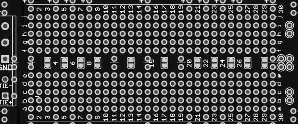
Breadboards are essential components for technicians looking to set up DIY electronics connections. These simple yet pretty useful gadgets help beginners and amateurs acquaint themselves with electronic circuits in the comfort of their homes. Doing so allows them to master the art of circuitry within a short time and without having to strain a lot.
Moreover, experts utilize these gadgets to test circuits before integrating them into larger projects. Doing so helps them catch errors in the circuitry early before using it on the larger project, which helps them save on damages.
https://www.youtube.com/watch?v=bZM2KDX221o
There are two breadboards in the market today, solderable and solderless. And just as the names dictate, solderless breadboards help technicians make simple circuits without having to solder cables onto the board. On the other hand, solderable breadboards tend to be more complex as technicians can solder cables to make permanent connections. However, even though they are complex, solderable breadboards help technicians make connections that last longer. Hence they are pretty beneficial in the long run. Therefore, we shall focus on the solderable breadboards and everything that makes these boards unique.
Solderable breadboards contain holes that you can utilize to connect electronic components onto the board. After connecting the necessary electronic component, you can then solder the components onto the board using a soldering iron. The soldering iron connects the electrical components onto the board’s copper tracing, making a permanent connection.
On the other hand, if you want to design a simple circuit, you will require jumper cables. These jumper cables will act as a link between different components. However, you will have to solder each jumper cable separately and between the components. After doing so, these jumper cables will let current flow from one element to another, generating a nice circuit.
Moreover, solderable breadboards come in varying sizes. Therefore, you can select the size that suits your project.
Advantages of utilizing a Solderable Breadboard over Solderless
When working with a solderable breadboard, you are going to enjoy the following benefits:
Robustness
Solderable breadboards tend to be pretty robust. Therefore, you can explore different circuitries on these boards without feeling as if you are pushing the board too much.
Moreover, these boards help you make permanent connections that do not come apart quickly. Therefore, you can create complex circuitries without worrying about specific components falling off.
Custom look
Solderable breadboards help you develop circuits that have a custom look. Therefore, if you utilize these components in your project, you can always be sure that the results will be unique.
Time and Cost Saver
Solderable breadboards help you save on time and cost. That is because these breadboards create a permanent circuit that stays functional for longer. You hence don’t have to make reconnections to test out your circuits.
Since solderable breadboards make permanent circuits, you can only utilize them once. Therefore, you can’t reuse them on other projects.
Repairing
If you make a mistake when soldering components onto the breadboard, repairing the error might do more bad than good to the board. That is because the process of de-soldering tends to damage the breadboard and the component alike. Hence, when working with solderable breadboards, you should be extra careful and avoid errors at all costs.
The Connection Layout of a Solderable Breadboard
Solderable breadboards typically include several connection holes (tiny sockets) that technicians utilize to make connections. These small holes have a 0.1 grid arrangement on the breadboard, which leaves enough space to make connections.
Moreover, most electrical components that technicians utilize on these breadboards come bearing connection terminals. These are the terminals that you place directly inside the connection holes to connect an electrical component to the board. To secure the component, you have to solder the terminals to the board’s copper traces.
Also, when connecting ICs (integrated circuits), you must arrange them across the center gap through their notch or dot to the left.
On the other hand, when designing a jumper cable, you must utilize a wire bearing a plastic coating. Doing so reduces the chances of short circuits occurring, potentially damaging the board. Moreover, the jumper cable must have a diameter of about 0.6mm for easier handling.
Tips to make use of when working with a Solderable Breadboard
Wires
Avoid using stranded wires on the breadboard when working with a solderable breadboard. That’s because stranded wires tend to be thick, which makes them challenging to manipulate.
Instead, it would help if you opted to utilize jumper or solid core cables. These cables are durable, thin, and easy to manipulate when creating connections on the board.
Joining Solderable Breadboards
If you are working on a large project, you can easily merge two solderable breadboards to generate more working area. Doing so can save you a lot of time and make your project look neat and custom.
Jumper Cables
Do not throw away the wires you cut when cutting capacitors and resistor lead. Instead, you can utilize these cables as jumper cables saving time and money.
Moreover, these component terminals have a nice core and are great conductors of electricity. Plus they tend to be easy to manipulate making them great jumper cables.
Type of Solder to utilize
Two varieties of solder exist that you can utilize on a breadboard:
Lead and Tin solder
Tin and silver solder (lead-free)
You can utilize any of these solder components on a solderable breadboard with little to no hassle. However, it would help if you remembered that tin and silver solder require more heat to melt. Therefore, you must utilize a high-wattage soldering iron to do the job.
Conclusion
Solderable breadboards are pretty helpful in the electrical industry. Their time and money-saving characteristics make them a go-to product to multiple individuals. Moreover, since their connections are permanent, they ease portability issues. Therefore, if you are in a dilemma regarding the type of breadboard to utilize, we suggest you try the solderable breadboard. It makes your job easier and better in the long run.
An electronic component comprises one or more discrete elements that work together to form an electronic circuit. Each element has a unique function and belongs to passive and active groups. The main function of a discrete component is to control the flow of current and to perform computation or amplification of a signal. These components are helpful in various applications, including calculators, personal computers, printers, scanners, and home appliances.
Electronic components consist of different materials. The main difference between these materials is their physical characteristics. Some components are passive, while others are active and electromechanical. For example, according to strict physics definitions, batteries are considered active components since they are energy sources. Other active components are electrical components, like transistors, triode vacuum tubes, or tunnel diodes.
Electronics components are made of different materials, depending on their purpose. The most basic features are diodes and resistors. These components are used in electronic circuits and change electric currents to carry information. Active electronic components contain gain, which allows them to add energy to a circuit. On the other hand, passive components cannot add energy to the circuit.
An integrated circuit is a series of electrical components connected by wires or electromagnetic connections. Electrolytic capacitors contain more charge per unit volume and are helpful for high-current circuits.
There are several distributors in the world. Some of them have large databases of parts and components. Others specialize in specific industries or products. Some have technical support available. In addition, the information needed by companies is increasingly available on the internet. In some cases, distributors have a dedicated technical support department to help customers troubleshoot and resolve issues.
RS Components
RS Components is one of the largest electronic component distributors in the world. Their comprehensive inventory includes more than 135,000 different product lines. Their worldwide presence allows them to serve customers in more than 40 countries. With an order fill rate of nearly 98 percent, RS Components delivers parts to their customers in 5-7 business days. They also offer free doorstep delivery, which is convenient for their customers. In addition, they are committed to supporting their customers and are actively involved in various community initiatives. For instance, RS recently launched an initiative called Okdo, which combines hardware and software to support the Internet of Things (IoT).
RS Components is an industrial and electronic component distributor that serves customers globally. Its network of over 2,500 suppliers enables it to provide a wide selection of electronic components and electronic parts. This company also provides value-added services to help customers find the right components to meet their unique needs. The company supports its customers across the entire product life cycle, from concept to production.
To remain competitive, companies in the electronic components industry must create a robust vision, plan, and omnichannel strategy to stay ahead of the Amazon Business threat. It may even require transforming the way they do business. If not, they may find themselves becoming obsolete. So it is essential to take action now to protect their business.
If you need electronic components, you can find them at RS Components, Mouser, Digi key, and other online electronics component distributors. These companies have more than 50 lakh products online from leading worldwide manufacturers. They also provide IT solutions to their customers. This makes them one of the largest electronic component distributors.
BD Electronics Ltd is one of the largest global distributors of electronic components. The company offers worldwide shipping, competitive prices, and prompt service. Its services are flexible and can customize for the US, Europe, and Asia. In addition, it has an email address protected from spam bots, so you can be confident that you will receive relevant emails to your business.
BD Electronics also utilizes an LTB notice to secure newly obsolete components. However, this only works if the PCN’s last buy and ship dates are far ahead to place an order. Despite these limitations, BD Electronics continues to maintain a large inventory of various electronic components.
Samsung Semiconductor
Samsung Semiconductor is a multinational company that manufactures various electronic components. The company is headquartered in South Korea but has operations worldwide. Its products help enrich lives and improve industrial efficiency. The company also distributes electronic components to many other companies.
Samsung Semiconductor has experienced a recent upturn in the semiconductor industry. The company posted a 19 percent jump in semiconductor sales in the second quarter of this year. The company has also become the world’s largest supplier of memory ICs, surpassing Intel in this area.
Lee Kun-hee, the founder of the company, believed that high-tech electronics would be the future growth industry. So he founded the company in 1978 and began working with foreign companies to develop advanced semiconductor technologies. Finally, in 1983, the government of South Korea forced foreign telecommunications equipment manufacturers to give Samsung their technology, giving the company access to the Korean market. As a result, the company acquired proprietary technology from Japanese and American semiconductor companies.
Samsung Semiconductor is a wholly owned subsidiary of the Samsung Group, the largest electronics manufacturer in Asia. Its products include televisions, telecommunications equipment, computers, and semiconductors. It also provides advanced process design to fabless companies. Its subsidiaries include the Samsung Display Company, the world’s largest producer of LCD and OLED displays.
Its semiconductor business continues to generate high profits. However, its smartphone division has struggled over the past few years. So although the company still makes high profits in this area, it needs to look for new businesses to increase profits. The semiconductor business is just one part of Samsung Electronics’ revenue, but it is a significant part of its business.
Future Electronics is one of the largest electronic component distributors in the world. It was founded in 1968 and has become a leading global force in the industry. Future Electronics has 5,000 employees working in 169 offices in 44 countries. IT infrastructure helps it maintain real-time inventory availability and fully integrates operations.
Founded by Robert Miller in 1968, Future Electronics is one of the most innovative companies in the electronics industry. It is the largest distributor of semiconductors, including discrete transistors, field-emitter transistors, and integrated circuits. The company is headquartered in London and has offices in the United States, Canada, and Europe.
The company is considered one of the most reliable distributors of electronic components. It received high customer ratings and is ranked number one in a recent survey by EBN. Customers ranked it as the number one distributor, garnering 68% of the vote. In addition, it offers a comprehensive range of electronic components and services.
The company’s growth and success are due to its strong supply chain, technical knowledge, and competitive pricing. The company successfully overcame supply chain disruptions and challenges during the past year. However, several obstacles have impacted its growth in recent years. Fortunately, it has managed to remain competitive despite its challenges.
Electronic component distributors are essential elements of the electronic supply chain. They help manufacturers by allowing them to buy the necessary components and schedule deliveries. Furthermore, electronic component distributors provide valuable services such as introducing new components. This is vital for development and manufacturing companies looking for the latest components.
Factors to Consider When Choosing the Electronic Component Distributor
One of the key factors in selecting an electronic component distributor is the type of components it offers. There are several different types of distributors, each focusing on a specific type of component. For example, an RF and microwave distributor will stock specialized components that are hard to find elsewhere. Specialized distributors also offer a unique service, such as arranging for the supply of components. These types of distributors usually carry no inventory and fill a niche in the market.
Reliability
When choosing an electronic component distributor, choosing a company with high reliability is essential. Sending back a component because of a quality issue wastes time. Make sure that the company you choose offers precise contact details. You should always be able to reach them directly if you have questions or need more information about a particular component. You should also look for a company with advisors and online chat options.
Choosing a reputable electronic component distributor is essential for the success of any PCB project. Without reliable suppliers, designers cannot create new prototypes or keep track of changes in the supply chain. Also, it is difficult to predict the future of the PCB market. Therefore, you must choose a distributor carefully and use the data to make the right decision.
Cost
When choosing an electronic component distributor, you should look for one with an extensive inventory. A distributor with a large inventory will be able to provide your company with the components it needs on a timely basis. This is particularly important if you are facing an emergency. Also, if you have to make a quick purchase, selecting a distributor with a large inventory will help you meet the deadline.
Electronic component prices can vary widely. This is primarily due to the materials used to manufacture the part. Cheaper materials can result in cheaper electronic components, while components with higher quality materials will be more expensive. Another factor that influences pricing is the part’s product life-cycle. Some components have a short lifespan, while others can last for decades. In some cases, distributors discount their prices to clear large inventories of obsolete parts.
Choosing the right distributor for your needs can help you manage the life cycle of your electronic products. This allows you to focus on the features of next-generation products instead of worrying about what will happen to your current components.
Life-cycle considerations include the type of components you require and the availability of alternatives. For example, a low-cost component might be available for a short time but might be obsolete in a few years. For a long-term solution, look for components with a minimum 5-year availability period.
One of the biggest challenges facing electronics manufacturers is the obsolescence of parts. As a result, manufacturers must implement an intelligent obsolescence strategy to ensure that they don’t face a supply chain crisis by being unable to replace parts. Luckily, a solid distribution partnership can help smooth out this process.
Traceability
In the modern world, manufacturers are trying to reduce costs and increase the efficiency of their operations, and traceability is an essential factor to consider. But, it is important to understand the challenges in implementing traceability. One of these challenges is that different companies approach data management differently. This creates communication barriers because different departments use different terminology.
The goal of comprehensive traceability is to connect data from raw materials, manufacturing processes, and products to their source. This helps to ensure the quality of the end product. It also helps to increase customer confidence and trust.
Quality
As an electronic component distributor, you must ensure that you get high-quality components. Counterfeit parts can cause serious damage to your revenue and brand. They can also cause your product to malfunction or fail. To avoid this, you must choose quality management and counterfeit mitigation program distributor. Such programs help distributors identify and control counterfeit parts’ risks and report fraud. These measures also help maintain the integrity of the supply chain.
Choosing a distributor that follows industry standards and participates in industry associations and governing bodies is essential. For example, if the distributor is an Electronic Components Industry Association (ECIA) member, they will know the latest industry standards. Additionally, a distributor should be a member of the Government-Industry Data Exchange Program (G-IDEP).
There are many types of Electronic Component Distributors. Some specialize in a particular type of electronic component, while others are more generalized in their offering. In either case, the distributor can be an essential partner for customers and component manufacturers. In addition, these companies stock many components, including discrete transistors, FETs, and integrated circuits. As a result, they can supply virtually any electronic component, including those not typically found in a single location.
In this case, the company is trying to expand its customer base and maintain its competitive position in the market. One way to do this is to customize the products that they distribute. Adding a unique feature to the product can draw consumers’ attention and help a business occupy a significant market position.
As the industry continues to grow and mature, these companies are also introducing new technologies to compete in a competitive environment. These new technologies can reduce costs, enhance existing products, and introduce new products. In addition, they are expanding their reach and establishing production facilities in different regions. This geographic expansion can improve sales.
If you are looking for an excellent electronic component distributor, it is essential to consider the size and volume of your project. For example, you may need a lot of a particular component type. On the other hand, if you need many specific components, you might want to find one with a large inventory and good customer service.