How to Design a Connector Pinout For Your PCB

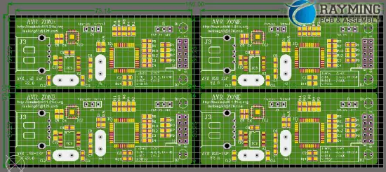
In the world of printed circuit board (PCB) design, connectors play a crucial role in facilitating communication and power transfer between various components and systems. The pinout, or the arrangement of pins on a connector, is a critical aspect that requires careful planning and consideration. A well-designed connector pinout can ensure reliable signal integrity, optimize PCB layout, and simplify assembly and maintenance processes.

This article will guide you through the essential steps and best practices for designing an effective connector pinout for your PCB. By following these guidelines, you can create a pinout that not only meets your project’s functional requirements but also adheres to industry standards and promotes efficient and robust design practices.

Understanding Connector Pinout Design

A connector pinout is the arrangement of pins or terminals on a connector, which defines the signal, power, and ground connections between the PCB and other components or systems. The pinout design process involves assigning specific signals or functions to each pin, considering factors such as signal integrity, power delivery, and grounding requirements.

Designing an effective connector pinout is crucial for several reasons:

  1. Signal Integrity: Proper pinout design can minimize crosstalk, electromagnetic interference (EMI), and other signal integrity issues, ensuring reliable data transmission and minimizing potential signal degradation.
  2. Power Delivery and Grounding: Appropriate placement of power and ground pins can ensure proper power distribution and effective grounding, reducing noise and improving overall system performance.
  3. Layout Optimization: A well-planned pinout can simplify PCB layout, reduce trace lengths, and minimize routing complexities, leading to a more efficient and compact design.
  4. Compatibility and Standardization: Adhering to industry standards and conventions for connector pinouts can ensure compatibility with existing systems and facilitate integration with third-party components or peripherals.
  5. Assembly and Maintenance: A logical and consistent pinout design can simplify the assembly process, reduce the risk of errors, and facilitate easier troubleshooting and maintenance.

Step-by-Step Guide to Designing a Connector Pinout

Follow these steps to design an effective connector pinout for your PCB:

1. Identify Connector Requirements

Begin by identifying the specific requirements for your connector, including the number of signals, power, and ground connections needed. Consider factors such as data rates, voltages, and current requirements. Additionally, determine any special requirements, such as shielding or specific connector types (e.g., USB, HDMI, or proprietary).

2. Select the Appropriate Connector Type

Choose the connector type that best suits your requirements, considering factors such as the number of pins, pitch (spacing between pins), and physical dimensions. Common connector types include headers, D-subminiature, RJ-45, and specialized connectors for specific applications.

3. Assign Signal Types

Categorize the signals based on their types, such as differential pairs, single-ended signals, power, and ground. Group related signals together, as this can simplify routing and reduce crosstalk.

4. Apply Signal Integrity Principles

Consider signal integrity principles when assigning pin positions. For example, separate high-speed differential pairs from single-ended signals to minimize crosstalk. Additionally, group high-speed signals together and place them away from power and ground pins to reduce electromagnetic interference (EMI).

5. Implement Power and Ground Strategies

Implement effective power and ground strategies by strategically placing power and ground pins. Distribute power and ground pins evenly across the connector to ensure proper power delivery and grounding. Consider using dedicated power and ground planes or polygons for high-current applications.

6. Follow Industry Standards and Conventions

Adhere to industry standards and conventions for connector pinouts whenever possible. Many connector types have established pinout standards, which can ensure compatibility and interoperability with other systems and components.

7. Consider Physical Layout Constraints

Take into account the physical layout constraints of your PCB when assigning pin positions. Minimize trace lengths by placing pins closer to the corresponding components or routing channels. Consider the routing complexity and potential obstacles, such as vias or component placements.

8. Implement Consistency and Documentation

Maintain consistency in your pinout design across multiple connectors or products within the same family or series. Document your pinout design thoroughly, including signal assignments, power and ground connections, and any special considerations or conventions used.

9. Perform Signal Integrity Simulations

For high-speed or critical applications, consider performing signal integrity simulations or analyses to validate your pinout design. These simulations can help identify potential issues, such as crosstalk, impedance mismatches, or EMI concerns, allowing you to make necessary adjustments before finalizing the design.

10. Review and Iterate

Once you have completed the initial pinout design, review it thoroughly with your team or stakeholders. Iterate and refine the design as needed based on feedback, additional requirements, or any identified issues.

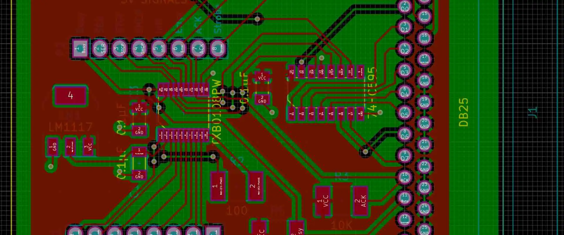
Example Connector Pinout Table

pcb-connectors-wire-to-board

To illustrate the importance of a well-designed connector pinout, consider the following example table for a high-speed digital interface connector:

Pin NumberSignal NameSignal TypeDescription
1TX+Differential PairTransmit Data Pair (Positive)
2TX-Differential PairTransmit Data Pair (Negative)
3RX+Differential PairReceive Data Pair (Positive)
4RX-Differential PairReceive Data Pair (Negative)
5GNDGroundGround Reference
63.3VPower3.3V Power Supply
7GNDGroundGround Reference
8CLK+Differential PairClock Pair (Positive)
9CLK-Differential PairClock Pair (Negative)
10GNDGroundGround Reference

In this example, the differential pairs (TX+/TX-, RX+/RX-, and CLK+/CLK-) are grouped together and separated from the single-ended signals (power and ground) to minimize crosstalk. Power and ground pins are evenly distributed across the connector, ensuring proper power delivery and grounding. Additionally, ground pins are placed adjacent to high-speed differential pairs to provide a reference and reduce EMI.

FAQs (Frequently Asked Questions)

  1. Why is connector pinout design important in PCB design? Connector pinout design is crucial because it directly impacts signal integrity, power delivery, grounding, layout optimization, compatibility, and ease of assembly and maintenance. A well-designed pinout can ensure reliable performance, minimize interference, and simplify the overall design process.
  2. How do industry standards and conventions influence connector pinout design? Industry standards and conventions for connector pinouts are essential for ensuring compatibility and interoperability with existing systems and components. Following these standards can facilitate integration with third-party devices, simplify documentation, and promote consistency across different designs or product lines.
  3. What are some common signal integrity issues related to connector pinout design? Common signal integrity issues related to connector pinout design include crosstalk, electromagnetic interference (EMI), impedance mismatches, and ground loops. Proper pinout design, with considerations for signal separation, grounding strategies, and shielding, can help mitigate these issues.
  4. How can connector pinout design affect PCB layout and routing? The connector pinout design can significantly impact PCB layout and routing. Strategic pin assignments can minimize trace lengths, reduce routing complexities, and optimize the overall PCB footprint. A well-planned pinout can simplify the layout process and promote efficient use of PCB real estate.
  5. Can signal integrity simulations aid in connector pinout design? Yes, signal integrity simulations and analyses can be valuable tools in connector pinout design, especially for high-speed or critical applications. These simulations can identify potential issues, such as crosstalk, impedance mismatches, or EMI concerns, allowing designers to make informed adjustments to the pinout before finalizing the design.

Designing an effective connector pinout is a critical step in the PCB design process. By following the guidelines outlined in this article, you can create a pinout that ensures reliable signal integrity, optimizes power delivery and grounding, simplifies PCB layout, and adheres to industry standards and best practices. A well-designed connector pinout not only enhances the performance and reliability of your PCB but also facilitates easier assembly, maintenance, and integration with other systems and components.

Most Important Points of Budgetary Quote Early in the Design Process

Modular PCB Design

In the world of product development, one of the most critical steps is obtaining an accurate budgetary quote early in the design process. This quote serves as a valuable tool for stakeholders, allowing them to assess the feasibility and viability of the project, allocate resources effectively, and make informed decisions. A well-prepared budgetary quote can help mitigate potential cost overruns, ensure smooth project execution, and ultimately contribute to the success of the final product.

This article will explore the most important points to consider when requesting a budgetary quote early in the design process. By understanding these key factors, you can obtain a more accurate and comprehensive estimate, enabling you to plan and allocate resources more effectively.

Understanding the Importance of Budgetary Quotes

A budgetary quote is a preliminary estimate of the costs associated with a project or product development. It provides a rough approximation of the expenses involved, including materials, labor, manufacturing processes, and other relevant factors. Obtaining a budgetary quote early in the design process offers several benefits:

  1. Cost Assessment: A budgetary quote allows stakeholders to evaluate the financial viability of the project and determine whether it aligns with their budget and business goals.
  2. Resource Allocation: By having an initial cost estimate, companies can allocate the necessary resources, such as funding, personnel, and equipment, more effectively.
  3. Risk Mitigation: An early budgetary quote helps identify potential cost risks and allows for proactive measures to be taken to mitigate or manage those risks.
  4. Decision-Making: With a clear understanding of the estimated costs, stakeholders can make informed decisions about proceeding with the project, modifying the design, or exploring alternative options.
  5. Supplier and Vendor Selection: A budgetary quote can assist in the selection of suitable suppliers and vendors based on their pricing and capabilities, ensuring a better fit for the project’s requirements and budget.

Key Points to Consider for Budgetary Quotes

To obtain an accurate and comprehensive budgetary quote, it is crucial to provide as much relevant information as possible to the manufacturer or supplier. The following points should be considered and addressed when requesting a budgetary quote:

1. Design Specifications and Requirements

Provide detailed design specifications, including drawings, schematics, bill of materials (BOM), and any other relevant documentation. Clear and concise specifications are essential for the manufacturer to accurately assess the complexity of the project and estimate the associated costs.

2. Materials and Components

Specify the types of materials and components required for the product, including their grades, finishes, and any special requirements. This information will help the manufacturer determine the appropriate material costs and any potential challenges or complexities associated with sourcing or processing the materials.

3. Manufacturing Processes

Outline the manufacturing processes required for your product, such as machining, molding, assembly, testing, and packaging. Each process may have different cost implications, and providing this information will enable the manufacturer to estimate the necessary resources and associated costs accurately.

4. Quantity and Production Volume

Indicate the anticipated production volume or quantity required. This information is crucial as it affects economies of scale and can significantly impact the overall cost per unit. Manufacturers may offer discounts or special pricing for larger production volumes.

5. Regulatory Compliance and Certifications

If your product requires specific regulatory compliance or certifications (e.g., CE, UL, ISO), mention these requirements in your request for a budgetary quote. Compliance and certification processes may involve additional testing, documentation, or specialized processes, which can affect the overall cost.

6. Delivery and Logistics Requirements

Specify any specific delivery or logistics requirements, such as packaging, labeling, or transportation needs. These factors can influence the overall cost and should be considered in the budgetary quote.

7. Timeline and Lead Times

Provide an expected timeline or desired lead time for the project. Manufacturers may need to factor in additional costs for expedited production or rush orders, which can impact the overall cost estimate.

8. Intellectual Property and Confidentiality

Address any intellectual property or confidentiality concerns upfront. This will ensure that the manufacturer understands the necessary precautions and potential costs associated with protecting your design or proprietary information.

9. Quality Control and Inspection Requirements

Outline any specific quality control or inspection requirements for your product. Additional testing, inspection, or verification processes may incur additional costs that should be accounted for in the budgetary quote.

10. Potential Risks and Contingencies

Identify any potential risks or contingencies that may arise during the project, such as supply chain disruptions, material shortages, or unforeseen technical challenges. Discussing these potential issues upfront can help the manufacturer provide a more comprehensive and realistic cost estimate.

By considering and addressing these key points when requesting a budgetary quote, you can ensure that the manufacturer has a comprehensive understanding of your project’s requirements and can provide a more accurate cost estimate. This, in turn, will enable you to make more informed decisions and allocate resources effectively throughout the design and development process.

Table: Comparison of Budgetary Quote Scenarios

To illustrate the importance of providing comprehensive information for budgetary quotes, consider the following table comparing three scenarios:

ScenarioInformation ProvidedAccuracy of QuotePotential Risks
1Basic design specifications, materials, and quantityLowHigh risk of cost overruns, delays, and quality issues
2Detailed design specifications, materials, processes, and quantityModeratePotential risks related to compliance, logistics, and unforeseen challenges
3Comprehensive information covering all key pointsHighMinimal risks, as potential challenges have been addressed upfront

As the table demonstrates, providing comprehensive information in scenario 3 leads to a highly accurate budgetary quote and minimizes potential risks, enabling better planning, resource allocation, and decision-making throughout the design and development process.

FAQs (Frequently Asked Questions)

  1. When is the best time to request a budgetary quote? It is recommended to request a budgetary quote as early as possible in the design process. This allows stakeholders to assess the financial viability of the project and make informed decisions before committing significant resources. Early budgetary quotes can also identify potential cost-saving opportunities and enable proactive planning.
  2. How accurate are budgetary quotes? The accuracy of a budgetary quote depends on the level of detail and information provided. A comprehensive budgetary quote that includes detailed specifications, manufacturing processes, and potential risks will generally be more accurate than a basic quote with limited information. However, it’s important to note that budgetary quotes are still estimates and may be subject to changes as the project progresses.
  3. Can a budgetary quote be revised or updated? Yes, budgetary quotes can be revised or updated as more information becomes available or if there are changes to the project requirements or specifications. It is advisable to communicate any changes or updates to the manufacturer promptly to ensure that the budgetary quote remains accurate and up-to-date.
  4. What factors can cause discrepancies between the budgetary quote and the final cost? Discrepancies between the budgetary quote and the final cost can arise due to various factors, such as changes in material costs, unforeseen technical challenges, supply chain disruptions, changes in regulatory requirements, or underestimated labor costs. Providing comprehensive information upfront can help minimize these discrepancies.
  5. Can a budgetary quote be used for supplier or vendor selection? Yes, budgetary quotes can be used as part of the supplier or vendor selection process. By obtaining budgetary quotes from multiple manufacturers or suppliers, you can compare pricing, capabilities, and services offered, ensuring that you select the best fit for your project’s requirements and budget.

Obtaining an accurate budgetary quote early in the design process is a critical step that should not be overlooked. By providing comprehensive information and considering the key points outlined in this article, you can ensure a more reliable cost estimate, facilitate effective resource allocation, and make informed decisions throughout the product development lifecycle.

PCB Via Current-Carrying Capacity: Is My PCB Too Hot?

In the world of printed circuit board (PCB) design, one of the critical factors that can significantly impact the performance and reliability of a circuit is the current-carrying capacity of vias. Vias are the small plated-through holes that interconnect different layers of a PCB, allowing for the flow of electrical signals and power. However, when these vias are subjected to excessive current loads, they can generate significant heat, potentially leading to thermal issues and even PCB failure.

Understanding the current-carrying capacity of vias is crucial for ensuring the proper thermal management of your PCB design. In this article, we will delve into the factors that affect via current-carrying capacity, explore thermal management strategies, and provide practical tips to help you determine if your PCB is running too hot.

Understanding Via Current-Carrying Capacity

The current-carrying capacity of a via is determined by several factors, including its physical dimensions, the materials used in its construction, and the thermal environment in which it operates. When current flows through a via, it encounters resistance, which results in the generation of heat. The amount of heat generated is directly proportional to the current flowing through the via and its resistance.

1. Via Dimensions

The physical dimensions of a via, such as its diameter and length (thickness of the PCB), play a crucial role in determining its current-carrying capacity. Generally, larger diameter vias have a lower resistance and can carry higher currents without overheating. Similarly, shorter vias have lower resistance and can dissipate heat more effectively than longer vias.

2. PCB Materials

The materials used in the construction of the PCB can also affect the current-carrying capacity of vias. Different materials have varying thermal conductivity properties, which influence their ability to dissipate heat. For example, PCBs made of materials with high thermal conductivity, such as aluminum or copper, can effectively dissipate heat generated by vias, allowing them to carry higher currents.

3. Thermal Environment

The thermal environment in which the PCB operates plays a significant role in determining the current-carrying capacity of vias. Factors such as ambient temperature, airflow, and the presence of heat sinks or cooling systems can greatly impact the ability of vias to dissipate heat effectively.

Calculating Via Current-Carrying Capacity

High Current PCB

Several methods and guidelines exist for calculating the current-carrying capacity of vias. One widely used approach is the IPC-2221 standard, which provides equations and tables to estimate the current rating of vias based on their dimensions and the materials used.

The IPC-2221 standard considers factors such as via diameter, plating thickness, copper weight, and the thermal resistance of the PCB materials. It provides equations to calculate the maximum current that can flow through a via without exceeding a specified temperature rise.

Another method for estimating via current-carrying capacity is through thermal simulation and analysis. Computer-aided design (CAD) tools and finite element analysis (FEA) software can be used to model the thermal behavior of vias under various current loads and environmental conditions. These simulations can provide valuable insights into the thermal performance of your PCB design and help identify potential hotspots or areas of concern.

Thermal Management Strategies for Vias

If your PCB design involves high current loads or operates in a thermally challenging environment, implementing effective thermal management strategies is crucial. Here are some approaches to consider:

1. Via Array Design

Instead of relying on a single large via to carry high currents, designers often opt for via arrays or multiple smaller vias in parallel. By distributing the current across multiple vias, the heat generation is reduced, and the overall current-carrying capacity is increased.

2. Thermal Vias

Thermal vias, also known as heat vias or thermal relief patterns, are strategically placed vias that act as thermal conductors, helping to dissipate heat from hot components or areas of the PCB. These vias are typically connected to larger copper areas or heat sinks, providing an efficient path for heat transfer.

3. Thermal Planes

Incorporating thermal planes, or solid copper planes, into your PCB design can significantly improve heat dissipation. These planes act as heat spreaders, distributing the heat generated by components and vias over a larger area, reducing hotspots and improving thermal management.

4. Thermal Interface Materials

When working with high-power components or dense via arrays, the use of thermal interface materials (TIMs) can be beneficial. TIMs, such as thermal pads or thermal greases, improve the thermal coupling between the PCB and heat sinks or cooling systems, enhancing heat transfer and dissipation.

5. Active Cooling Solutions

In extreme cases or applications with very high current loads, active cooling solutions like fans or liquid cooling systems may be necessary to maintain acceptable operating temperatures for vias and other components.

Signs of Overheating in PCBs

Even with careful design and thermal management strategies, overheating issues can still occur in PCBs. It is essential to be aware of the signs that indicate your PCB may be running too hot, allowing you to take corrective actions before failures occur. Some common indicators of overheating include:

  1. Physical Damage: Discoloration, warping, or delamination of the PCB can be signs of excessive heat exposure.
  2. Component Failure: Premature failure of components, such as capacitors or integrated circuits, may be caused by overheating.
  3. Intermittent Operation: Circuits experiencing intermittent operation or glitches could be a result of thermal stress on components or vias.
  4. Thermal Imaging: Using thermal imaging cameras or sensors can provide a visual representation of hotspots on your PCB, allowing you to identify areas of concern.

FAQs (Frequently Asked Questions)

  1. How can I determine the current rating of a via in my PCB design? You can determine the current rating of a via by using the IPC-2221 standard equations or guidelines provided by the PCB manufacturer. These equations take into account factors such as via diameter, plating thickness, copper weight, and the thermal resistance of the PCB materials. Alternatively, you can perform thermal simulations or finite element analysis to estimate the current-carrying capacity based on your specific design and environmental conditions.
  2. What are some common causes of via overheating? Common causes of via overheating include inadequate via dimensions (small diameter or excessive length), high current loads, poor PCB material selection (low thermal conductivity), lack of proper thermal management strategies, and harsh operating environments (high ambient temperatures or limited airflow).
  3. Can via arrays help mitigate overheating issues? Yes, using via arrays or multiple smaller vias in parallel can significantly improve the current-carrying capacity and reduce heat generation. By distributing the current across multiple vias, the heat generation is reduced, and the overall thermal performance is enhanced.
  4. How can thermal vias or thermal planes help with PCB thermal management? Thermal vias, also known as heat vias or thermal relief patterns, provide efficient paths for heat transfer from hot components or areas of the PCB to larger copper areas or heat sinks. Thermal planes, or solid copper planes, act as heat spreaders, distributing the heat generated by components and vias over a larger area, reducing hotspots and improving thermal management.
  5. When should I consider active cooling solutions for my PCB design? Active cooling solutions, such as fans or liquid cooling systems, may be necessary in extreme cases or applications with very high current loads or power densities. If passive cooling methods (e.g., heat sinks, thermal vias, and thermal planes) are insufficient to maintain acceptable operating temperatures, active cooling solutions should be considered to ensure reliable and safe operation of your PCB.

Proper thermal management and via current-carrying capacity considerations are crucial for ensuring the reliable operation and longevity of your PCB designs. By understanding the factors that affect via current-carrying capacity, implementing effective thermal management strategies, and monitoring for signs of overheating, you can mitigate the risk of thermal issues and create robust and high-performing PCB designs.

Rogers PCB Vs. Nelco laminates Vs. Taconic material Vs. Arlon: From Design,Manufacturing to Cost FOR Microwave Electronics

Rogers RO4500 PCB

In the realm of microwave electronics, the choice of materials for printed circuit boards (PCBs) is crucial for achieving optimal performance, reliability, and cost-effectiveness. Among the leading manufacturers of high-frequency laminates are Rogers Corporation, Nelco, Taconic, and Arlon. These companies offer a wide range of materials tailored for various microwave applications, each with its unique properties and characteristics. In this article, we will delve into the design, manufacturing, and cost considerations of these materials, providing a comprehensive comparison to assist engineers and designers in making informed decisions.

Introduction to High-Frequency Laminates

High-frequency laminates, also known as microwave laminates or RF substrates, are specialized materials used in the fabrication of PCBs for applications operating at high frequencies, such as microwave and radio frequency (RF) circuits. These materials are engineered to exhibit exceptional electrical properties, including low dielectric constant, low dissipation factor, and consistent performance over a wide frequency range.

Microwave electronics encompass a diverse range of applications, including telecommunications, radar systems, satellite communications, and aerospace electronics. The performance and reliability of these systems heavily rely on the quality of the PCB materials used, making the selection of the appropriate laminate a critical decision.

Rogers PCB Materials

Rogers AD255C PCB

Rogers Corporation is a renowned manufacturer of high-performance materials for various applications, including microwave electronics. Their PCB materials are widely used in the industry due to their excellent electrical properties and thermal stability.

1. Rogers PCB Material Overview

Rogers offers a comprehensive portfolio of PCB materials designed for microwave and RF applications, including:

  • RO3000ยฎ Series: Ceramic-filled hydrocarbon composites with exceptional electrical properties, suitable for high-frequency and high-speed digital circuits.
  • RT/duroidยฎ Series: Glass microfiber reinforced PTFE (polytetrafluoroethylene) laminates known for their low dielectric constant and low dissipation factor.
  • RO4000ยฎ Series: Hydrocarbon-based laminates with excellent dimensional stability and electrical properties for high-frequency and high-speed digital applications.
  • TC Series: Thermoset ceramic-filled composites designed for high-temperature and high-reliability applications.

2. Design and Manufacturing Considerations

Rogers PCB materials are engineered to meet the stringent requirements of microwave electronics. The design and manufacturing processes involve careful consideration of various factors, including:

  • Dielectric Constant: The dielectric constant of the material is a critical parameter that affects the propagation of electromagnetic waves. Rogers materials are designed to have a low and stable dielectric constant over a wide frequency range, enabling efficient signal transmission.
  • Dissipation Factor: The dissipation factor, also known as the loss tangent, represents the energy lost as heat in the material. Rogers materials exhibit exceptionally low dissipation factors, minimizing signal attenuation and ensuring efficient power transfer.
  • Thermal Conductivity and Coefficient of Thermal Expansion (CTE): Thermal management is crucial in microwave electronics. Rogers materials are designed with high thermal conductivity and low CTE to dissipate heat effectively and maintain dimensional stability under temperature variations.
  • Mechanical Strength and Dimensional Stability: The mechanical properties of Rogers materials, such as tensile strength and dimensional stability, ensure reliable performance and consistent electrical characteristics in demanding environments.

3. Cost Considerations

While Rogers PCB materials offer superior performance, they typically come at a higher cost compared to other laminate options. The advanced materials and specialized manufacturing processes contribute to the increased cost. However, for critical applications where high performance and reliability are paramount, the investment in Rogers materials can provide long-term benefits and cost savings through improved system performance and reduced maintenance requirements.

Nelco Laminates

Nelco N4000-13 High-Speed pcb

Nelco is a leading manufacturer of high-frequency laminates, offering a range of materials designed for microwave and RF applications.

1. Nelco Laminate Overview

Nelco’s product portfolio includes:

  • N4000 Series: Glass-reinforced hydrocarbon/ceramic composite laminates with low dielectric constant and dissipation factor.
  • N6000 Series: Woven glass-reinforced PTFE laminates with excellent electrical properties and thermal stability.
  • N8000 Series: Thermoplastic composites with low dielectric constant and dissipation factor, suitable for high-frequency applications.

2. Design and Manufacturing Considerations

Nelco laminates are engineered to meet the demanding requirements of microwave electronics, with a focus on electrical performance, thermal management, and mechanical properties. Key considerations include:

  • Dielectric Constant and Dissipation Factor: Nelco laminates are designed to maintain stable electrical properties over a wide frequency range, ensuring efficient signal transmission and low signal loss.
  • Thermal Conductivity and CTE: Nelco materials are engineered with high thermal conductivity and low CTE to dissipate heat effectively and maintain dimensional stability under temperature variations.
  • Mechanical Strength and Dimensional Stability: The mechanical properties of Nelco laminates, such as tensile strength and dimensional stability, are optimized to provide reliable performance in demanding environments.

3. Cost Considerations

Nelco laminates are generally more cost-effective than Rogers materials, while still offering excellent performance for many microwave and RF applications. The choice between Nelco and Rogers materials often involves weighing the trade-off between cost and performance based on specific application requirements.

Taconic Materials

Taconic is another leading manufacturer of high-frequency laminates, offering a wide range of materials tailored for various microwave and RF applications.

1. Taconic Material Overview

Taconic’s product portfolio includes:

  • TacCladยฎ Series: PTFE-based laminates with low dielectric constant and dissipation factor, suitable for high-frequency and high-speed digital applications.
  • TacQuikยฎ Series: Thermoset laminates with excellent electrical properties and thermal stability, designed for high-reliability applications.
  • TacSilยฎ Series: Silicone-based laminates with low dielectric constant and dissipation factor, suitable for high-frequency and high-temperature applications.

2. Design and Manufacturing Considerations

Taconic materials are engineered to meet the stringent requirements of microwave electronics, with a focus on electrical performance, thermal management, and mechanical properties. Key considerations include:

  • Dielectric Constant and Dissipation Factor: Taconic materials are designed to maintain stable electrical properties over a wide frequency range, ensuring efficient signal transmission and low signal loss.
  • Thermal Conductivity and CTE: Taconic materials are engineered with high thermal conductivity and low CTE to dissipate heat effectively and maintain dimensional stability under temperature variations.
  • Mechanical Strength and Dimensional Stability: The mechanical properties of Taconic materials, such as tensile strength and dimensional stability, are optimized to provide reliable performance in demanding environments.

3. Cost Considerations

Taconic materials are generally comparable in cost to Nelco laminates, offering a balance between performance and cost-effectiveness for many microwave and RF applications. The choice between Taconic and other manufacturers often depends on specific application requirements and performance trade-offs.

Arlon Materials

Arlon 55NT PCB

Arlon is a well-established manufacturer of high-frequency laminates, offering a range of materials suitable for microwave and RF applications.

1. Arlon Material Overview

Arlon’s product portfolio includes:

  • 25N Series: Woven glass-reinforced PTFE laminates with low dielectric constant and dissipation factor, suitable for high-frequency and high-speed digital applications.
  • 35N Series: Woven glass-reinforced hydrocarbon/ceramic composite laminates with excellent electrical properties and thermal stability.
  • AD Series: Thermoset laminates with low dielectric constant and dissipation factor, designed for high-reliability applications.

2. Design and Manufacturing Considerations

Arlon materials are engineered to meet the demanding requirements of microwave electronics, with a focus on electrical performance, thermal management, and mechanical properties. Key considerations include:

  • Dielectric Constant and Dissipation Factor: Arlon materials are designed to maintain stable electrical properties over a wide frequency range, ensuring efficient signal transmission and low signal loss.
  • Thermal Conductivity and CTE: Arlon materials are engineered with high thermal conductivity and low CTE to dissipate heat effectively and maintain dimensional stability under temperature variations.
  • Mechanical Strength and Dimensional Stability: The mechanical properties of Arlon materials, such as tensile strength and dimensional stability, are optimized to provide reliable performance in demanding environments.

3. Cost Considerations

Arlon materials are generally comparable in cost to other leading manufacturers in the microwave and RF laminate market. The choice between Arlon and other materials often depends on specific application requirements, performance trade-offs, and supplier relationships.

Comparison of Materials

To assist in the selection process, the following table provides a comparison of the key properties and characteristics of the materials discussed:

MaterialDielectric ConstantDissipation FactorThermal ConductivityCTEMechanical StrengthCost
Rogers PCB MaterialsVery LowVery LowHighLowExcellentHigh
Nelco LaminatesLowLowHighLowExcellentModerate
Taconic MaterialsLowLowHighLowExcellentModerate
Arlon MaterialsLowLowHighLowExcellentModerate

It’s important to note that the specific values of these properties may vary among different product lines within each manufacturer, and the selection should be based on the detailed material specifications and application requirements.

FAQs (Frequently Asked Questions)

  1. What are the key factors to consider when selecting a high-frequency laminate for microwave electronics? The key factors to consider include dielectric constant, dissipation factor, thermal conductivity, coefficient of thermal expansion (CTE), mechanical strength, dimensional stability, and cost. These factors directly impact the electrical performance, thermal management, and reliability of the microwave circuit.
  2. How do Rogers PCB materials compare to other laminates in terms of electrical performance? Rogers PCB materials, such as the RO3000ยฎ and RT/duroidยฎ series, are known for their exceptional electrical performance, with very low dielectric constant and dissipation factor. These materials offer superior signal transmission and minimal signal loss compared to many other high-frequency laminates.
  3. Are there any environmental or regulatory considerations when choosing a high-frequency laminate? Yes, environmental and regulatory considerations are important factors in material selection. Some manufacturers offer halogen-free and RoHS-compliant materials to meet environmental regulations. Additionally, certain applications may require materials with specific certifications or compliance standards.
  4. Can high-frequency laminates be used for flexible circuit applications? Yes, some manufacturers offer flexible high-frequency laminates that can be used for applications requiring flexible or conformal circuits. These materials combine the electrical properties of microwave laminates with flexibility and conformability.
  5. How does the cost of high-frequency laminates vary among different manufacturers? The cost of high-frequency laminates can vary significantly among different manufacturers. Generally, Rogers PCB materials are considered higher-cost options due to their advanced materials and specialized manufacturing processes. Nelco, Taconic, and Arlon laminates are typically more cost-effective while still offering excellent performance for many microwave and RF applications.

When selecting a high-frequency laminate for microwave electronics, it is crucial to consider the specific application requirements, performance needs, and cost constraints. Consulting with material experts and suppliers can help ensure the optimal choice for your design and manufacturing process.

What is LED Driver PCB?

A LED driver PCB houses the electronics necessary to operate LED lighting arrays safely and efficiently.

Key responsibilities include:

  • Regulate and transform supply voltage
  • Limit current through LEDs
  • Allow dimming control
  • Protect against faults

Understanding the special considerations for LED driving allows optimizing PCB design to achieve flicker-free long life lighting with reduced energy use.

Why LEDs Need Driver Circuits

LEDs characteristics necessitate additional circuitry:

Poor Voltage Regulation

LED forward voltage varies widely with temperature requiring compensation.

Low Reverse Breakdown

Small reverse voltages easily damage LEDs so polarity control and protection are vital.

Current/Luminosity Relationship

Precise current control directly impacts LED brightness so adjustable regulated current sources enable dimming.

Without drivers, LEDs are vulnerable while providing little analog control interface. So external driving electronics provide intelligent connection to the power supply.

Power Source Considerations

Common scenarios are constant or pulse-width modulated voltage sources, each with implications for driving needs:

AC Mains Power

Triac / relay based dimmers vary RMS voltage. Electronic converters generate regulated LED current from fluctuating supply.

DC Power

Wide voltage range DC requires buck, boost or buck-boost regulators for consistent LED drive voltage/current from fluctuating DC source like automotive or low voltage secondary supplies.

PWM Dimming Signal

Pulse-width modulated signals directly control LED brightness by gating current flow proportionally to duty cycle.

Accommodating various supplies and control interfaces adds complexity to driver PCB design.

Driver Architectures

led PCB Solution

Different configurations of power and control converter components achieve the LED current regulation. Here are some common driver architectures:

Linear vs Switch Mode Drivers

Linear uses an analog programmable resistor like a transistor between supply and LEDs.

  • Simple, low component count.
  • Wastes power as regulation element.
  • Large heat sinking.

Switch Mode chops fixed supply into adjustable high frequency pulses using inductors, capacitors and control ICs.

  • More efficient conversion.
  • Faster response for PWM dimming.
  • Generates EMI requiring suppression.

Dimming Approach

Resistor Control
Varies reference resistor setting output current magnitude.

PWM Control
Switches driver using external PWM signal ratio controlling mean LED current.

Analog Control Uses voltages or potentiometers to adjust output current.

AC vs DC Input Drivers

AC
Steps down and rectifies AC mains voltage then regulates current for LEDs.

DC
Buck, boost or inverting converters regulate fixed DC voltage to LED arrays directly. Simpler but less universal input range.

Series vs Parallel Output

Series strings multiple LEDs with single current ensuring uniformity.

Parallel drives multiple strings independently allowing zone control but needs current balancing.

Combinations or hybrid designs give optimized tradeoffs across cost, performance range and complexity depending on application needs for specialty matching LED arrays.

Typical Driver Circuitry

A typical LED driver PCB for 12V DC IN to 60V LED string OUT would contain:

AC/DC Input Stage

  • Fuse / Transient protection
  • Rectifier / smoothing capacitor
  • Power good detection

Intermediate Power Stage

  • Buck controller
  • MOSFET/Inductor step down
  • Freewheeling diode

Output Stage

  • Current sense resistor
  • Feedback amplifier
  • PWM reference generator
  • Open load detection

Auxiliary

  • Voltage reference
  • Compensation components
  • Diagnostic indicators

This handles wide DC input range down to controlled current output suitable for LED arrays. Multiple channels extend capacity driving more LED strings in parallel.

Cost Savings

Design choices balance performance versus unit costs through:

  • Choice of discrete power devices vs integrated controllers
  • Heat sinking approach – PCB copper relief versus external aluminum extrusion
  • Input surge protection level – simple clamping diode or multi-stage industrial grade
  • Conformal coating for environment protection or rely on enclosure sealing
  • Component adjustments to tune operating temperature range

Generally industrial grade components improve operating life but cost extra. The fixed development overhead is amortized across production volume allowing cost savings through simplified commercial grade designs where reliability risk is acceptable.

Improving Efficiency

Several techniques help maximize energy transfer to the LED load:

Low Loss Components

MOSFETS, inductors, sense resistors tailored for driver frequencies minimize switching and conduction losses.

Synchronization

Timing switch transitions to minimize shoot-through current when both NMOS/PMOS conduction overlaps.

Dead Time Control

Inserts brief delays between complementary switch transitions preventing any shoot-through risk.

Dimming Architectures

Stepping down both voltage and current during PWM dimming prevents wasted power across fixed resistors giving superior efficiency at lower brightness levels.

MethodTypical Efficiency Gain
Loss optimized components selection5%
Switch timing synchronization5%
Dimming architecture with variable resistor/supply15%

Gains through synchronization require fast accurate control loops to avoid glitches.

Reliability Enhancements

led pcb

Additional measures improve product reliability:

Thermal Derating

Run components below rated limits for operating lifetime improvement factors of 2-3X allowing extended warranty offerings.

Conformal Coating

Protects against humidity and contamination related leakage/corrosion especially in industrial or marine usage with risks of gases and fluids.

Over Temperature & Over Current Detection

Shutdown driver electronics rapidly on fault events before permanent LED damage. Assume LED itself lacks protection.

False Detection Immunity

Reasonable delays filtering noise induced fault triggers prevent unnecessary shutdown from transient spikes. Hysteresis on thresholds helps here too.

Component Screening

Pre-production qualification testing and burn-in eliminates early life failures.

Quality Assurance

Sample based final automated optical inspection and test coverage above 95% during volume ramp prevents factory escaped defects.

Careful design hardening prevents immediate returns or long term reliability degradation. But it increases validation overhead.

Design Tool Chain

Modern PCB solutions enhance development productivity:

Schematic Capture

Intelligent part selection, real time design rule checks and netlist generation with component data validation speeds error free translation from concept to layout.

Simulation

Time domain analysis captures switch mode power supply sequencing behaviors difficult to probe in hardware. Thermal modeling ensures sufficient heat spreading capacity.

Layout

Multi-layer autorouters with zone priority support rapid prototyping of complex multilayer stacks housing modern drivers and discrete thermal planes. Integrated 3D previews verify mechanical fit.

DFM Analysis

Quantitative process analysis highlights production risk areas like insufficient metal overlap on via farms prior to release. Suggests specific adjustments for high yield such as trace neckdowns.

Revision Control

Vaulting with managed release states dramatically eases change integration supporting ongoing maintenance improvements.

Investment in PCB design tools gives an amplifying effect on productivity over manual flows.

Conclusion

LED lighting greatly benefits from advanced electronic driver PCBs converting fluctuating supply into robustly regulated current ensuring consistent brightness over product lifetime at the best efficiency.

Voltage transformation, dimming interfaces and fault protection allow unlocking LED efficiencies. Furthermore programmable drivers support application tailored operation.

Cost sensitive commercial products make design choices trading off energy savings and diagnostics against tightly managed BoM costs and validation testing using an integrated tool chain accelerating time to market. The result is capable LED luminaires with previously impossible cost structures and 10X operational lifetime gains.

FAQ

Why are dedicated LED driver circuits needed?

LED efficiency and lifespan depends critically on precise current control. But LED voltage varies significantly with temperature while reverse polarity rapidly destroys them. So supplemental drive electronics provide robust voltage transformation, output regulation and protection enabling reliable lighting deployment.

What are the key subsystems within a LED driver?

Major building blocks are the front end AC or DC input power stage converting to regulated intermediate DC bus voltage,then an LED current regulation stage handles constant current or PWM controlled dimming power sent to LED arrays,finally protection subsystems avoid damage due to open loads or overheating through shutdown.

What are the tradeoffs between linear vs switch mode LED drivers?

Linear drivers offer simplicity with just an adjustable linear transistor element but waste significant power dropping excess voltage as heat. Switching methods use inductive energy storage for efficient conversion but require fast PWM controllers and generate EMI needing suppression filters adding costs.

How does driving topology differ for AC mains versus DC input power?

AC mains needs initial rectification and filtering to generate a DC bus followed by output regulation stages. For intermediate DC voltage sources, power factor correction is unnecessary simplifying driver stages to just voltage transformation and output regulation. But DC input range may be narrower.

What tools help accelerate LED driver PCB development?

Modern EDA packages with integrated schematic capture linked into simulation, autorouting layout editors with DFM analysis and version control streamline LED driver development lowering risks and time to market. Reusing verified circuit blocks also

Is Allegro PCB designer free?

Allegro PCB Designer is a leading professional printed circuit board (PCB) layout package developed by Cadence Design Systems. It provides sophisticated capabilities for electronics engineers to convert electronic schematics into physical board designs ready for fabrication.

Allegro is considered among the top tier of commercial PCB software thanks to advanced features like high-speed analog/RF layout, design for manufacturability analysis, team collaboration tools and integration with MCAD 3D mechanical CAD environments. It represents a major investment for organizations and is deployed widely across various industry verticals.

Naturally the superior sophistication of Allegro does come at significant financial cost when purchased outright for installation on corporate workstations or networks. So a common question raised is whether free or lower cost license options exist for access to such a powerful PCB design environment for applications like learning, evaluation or casual use.

Let’s fully explore what options both students and professional users have available when it comes to leveraging Allegro PCB technologies cost-effectively.

Commercial Allegro Licensing Approaches

For companies seeking to deploy Allegro for round-the-clock production PCB design activities powering their electronics hardware business, Cadence offers quite flexible purchasing models:

1. Perpetual License – One-time upfront capital payment to own license outright in perpetuity

2. Annual Lease License – Yearly operating lease fee providing latest software updates

3. Floating License – Shared pool allowing concurrent usage metering

In addition, various tiersSuch as Lite, Standard, Professional exist supporting different feature sets aligned to PCB design complexity needs. Academic versions for university instruction are also available.

But what about those on tighter budgets or individuals? Next let’s explore lower cost pathways for accessing Allegro capabilities.

Method 1 – Allegro Viewer for Read-Only File Examination

The Allegro Viewer application allows designers to freely view and interrogate Allegro board files (.brd) to examine layer stacks, design rules, component placements and other intelligent information present within completed layouts. This allows engineering teams to leverage data created by supply chain partners at no added cost.

However, the free Allegro Viewer strictly limits activity to READ-ONLY. No ability exists for editing, modification, exporting or generating production files like Gerbers. Just viewing for reference.

Still, access to scrutinize board databases offers helpful insights that facilitate discussions with assembly partners even without paying for full licenses. Where use cases involve just basic visualization or validation, the Allegro Viewer satisfies at no charge.

Now let’s consider options for students and hobbyists needing actual PCB layout creation capabilities on a budget.

Method 2 – Allegro Sigrity SI/PI Specialized Free Tool

Cadence offers completely free downloads targeted primarily at electrical engineering students and academics focused specifically on analysis of power distribution networks and signal integrity effects on high-speed digital PCBs.

The Sigrity PowerSI and Sigrity PowerDC tools specialize in simulations characterizing voltage drops, power plane resonance, decoupling capacitance needs and ensuring signal quality across entire board power systems. The Sigrity Signal Integrity tool concentrates directly on modeling high-speed buses, serdes links, clock trees and I/O timing analysis.

For aspiring PCB designers seeking relevant skill development, these sophisticated analysis tools offer great learning exposure. However, actual board layout functionality remains absent from the free offerings. Let’s keep searching for options.

Method 3 โ€“ Limited Term Free Trials

Cadence does periodically offer 30 or 60 day free full feature access to Allegro software for qualified professional users interested in test driving capabilities first hand before purchasing. Various limited promotions may run throughout the year for specific regions or verticals.

Individual hobbyists may also request trial access directly through their website form inquiries that get evaluated on a case by case basis for approval granting 1-2 months usage.

Such free trials allow substantial first hand working experience with most advanced features applied to a current real design project of value. Interested parties need to monitor for special opportunities periodically.

While helpful, temporary trials still leave a gap once expired though. Are there other alternatives?

Method 4 – Cloned Allegro-like Environments

Certain other competing PCB design packages intentionally developed similar graphical user interfaces, toolbars and keyboard shortcuts aiming to provide lower cost alternatives to Allegro that emulate its general experience:

Altium Designer โ€“ Highly capable electronics-focused ED tool

Eagle PCB Design Suite โ€“ Popular hobbyist/education package

KiCad EDA โ€“ Fully open source layout program

These clonish tool environments train users on skills more easily transferrable when migrating eventually to full scale Allegro implementation for advanced professional needs. Leveraging these platforms helps build relevant expertise.

But we have yet to uncover options granting enduring access to Cadence true Allegro apps without recurrent payments. Are any forever free PCB choices out there?

Method 5 โ€“ Older Releases Through Enthusiast Sharing

Among electronics hobbyist circles, certain unauthorized copies of obsolete pre-cloud era Cadence Allegro revisions (circa v16.2-17.4) still circulate via peer-to-peer sharing channels or vintage warez sites. These represent outdated offline perpetual licenses no longer supported or patched by Cadence publicly.

Tech savvy users may get these legacy versions running on modern systems through virtualization or compatibility mode workarounds. However Cadence understandably frowns on such practices that flout licenses. Plus missing decades of updates renders tools severely outdated.

Still for enthusiasts on severely constrained budgets seeking to experiment, old Allegro editions actually function surprisingly well despite dated interfaces and lack of current features if configured properly. Mint copies persisting on disks or images remain rare though.

Conclusion

In closing, while perpetual zero cost options donโ€™t officially exist for full modern Allegro PCB Designer suites from Cadence, quite a few pathways allow budget access for viewing production boards, targeted analysis tasks or time-bounded evaluations that facilitate skills development.

For academic instruction or manufacturing visualization, free limited apps get work done while low cost clone tools build familiarity for when careers lead eventually to advanced jobs justifying commercial Allegro investments. Staying resourceful pays off!

Frequently Asked Questions

Q: Does any free PCB software rival Allegro in capabilities?

A: No truly free tools offer comparable sophistication covering RF, flex/rigid and DFM needs adequately. But intermediate packages like Altium or KiCad still suffice reasonably for most mainstream boards if lacking top tier speed/precision. For ultra advanced requirements, only commercial tools like Allegro truly deliver.

Q: What risks exist trying older cracked Allegro copies?

A: Aside from legal concerns of using unauthorized software versions, running obsolete code past intended support lifetime brings cybersecurity vulnerabilities, absence of cloud license controls and lack of compatibility fixes that destabilize operations. Stick with legit free or trial tools only.

Q: Does Allegro Elements serve as a lower cost starter toolkit for learning?

A: No, Elements delivers Allegroโ€™s full professional toolset, just bundled at attractive pricing for emerging smaller firms. It omits no core features, serving as an excellent TCO ownership model that still requires commercial purchase.

Q: Can I export boards edited during a free trial if I donโ€™t continue using Allegro?

A: Fortunately Yes – well structured evaluations do allow retaining final design data in accessible formats to continue refinement with other tools later if migrating from the Cadence ecosystem after assessing capabilities delivered is deemed best practice.

Q: Where can I find the latest available free trial downloads or student learning versions?

A: Cadence modifies available options periodically. Check their website or contact regional sales representatives for recent promotinal offers if deadlines allow alignment to your project timeframe. Academic application forms qualify STEM educators always.

How To Get a Free altium viewer ?

Altium Designer 19 vs Altium Designer 18

Altium Designer is one of the most widely used printed circuit board (PCB) design software tools amongst engineers and hobbyists. However, the full licensed version carries a high price tag putting it out of reach for many casual users who simply need to view or open Altium PCB file formats.

Thankfully, Altium offers a functional free viewer that supports reading common file types generated from the Altium toolset. This allows broader access for sharing and reviewing board designs without requiring an expensive active license.

This article provides guidance on obtaining, installing and leveraging Altium’s zero-cost viewer alternative to enable PCB project visualization capabilities without financial burden.

Overview of Altium Design Software

Altium Designer represents complete, professional-grade electronics development software supporting every step of the PCB design process from schematic capture and simulation to board layout/routing all the way through to manufacturing output generations.

As a full lifecycle tool, Altium allows rapid translation of circuit concepts into physical boards ready for fabrication and component population. It streamlines development timelines through data-driven automation and integration. The unified environment reduces need to switch between disparate tools.

However, Altium requires paid license subscription on yearly basis to unlock the suite’s capabilities which presents cost barrier for many smaller organizations, students, and hobbyists. This is where the free viewer alternative steps in.

CategoryCapability
Design EntrySchematic capture & editing, HDL code development platform
SimulationMixed signal circuit simulation, analysis features
PCB LayoutMulti-layer routing/clearances, 3D viewing, MCAD collaboration
ManufacturingGerber & NC drill file generations, supply chain integrations

Table: Overview of Altium toolset categories and functionality

Altium Viewer Details

The Altium Viewer represents a freely distributed, installation-based application focused exclusively on allowing users to open, visualize, inspect, measure and navigate files generated from Altium Designer tools without ability execute edits.

It provides complete viewing access including:

  • Multi-layer 2D and 3D PCB viewing
  • Interactive board measurement
  • Drill-down from schematics to PCB layout layers
  • Flexible zooming/panning
  • DFM validation checking overlays
  • Component clearance checking
  • Linked navigation between schematic and PCB

The tool does not require licensing or activations once installed. However, saving data, exporting, or modifications are restricted. It suits teams needing to share, discuss, and critiques complete designs released from Altium Designer versus abstract representations. It also aids repair technicians tracing component placements.

For most visualization requirements, the Altium Viewer contains ample functionality at no cost burden.

Accessing the Free Viewer

Several options exist to obtain the free Altium Viewer installation package:

Direct Download

The viewer software can downloaded directly from Altium’s website via this link. Simply complete the brief registration form with email and company name to access the download page.

Request DVD

For those lacking reliable broadband internet connectivity, Altium can also mail a physical DVD with the Viewer upon request by contacting their regional customer service centers. However, this incurs greater delays.

Partner Hardware Extras

Selected hardware vendors distributing authorized partner versions of Altium sometimes bundle the Viewer into extras/accessories folders on installation disk images or as downloads incenting use of Altium file formats.

Regardless of specific access method, the viewer package itself remains standardized from Altium maintained at latest release.

SourceMediumProsCons
Altium WebsiteDirect digital downloadImmediate accessRegistration required
Altium Sales/SupportShipped DVDNo internet req’dShipping delays
Hardware Partner ExtrasDigitally bundledPotentially no separate downloadLacks standard packaging

Table: Overview of options to obtain the Altium Viewer installer

Installation Process

Once the Altium Viewer package has been acquired through one of the above methods, installing it follows common Windows application software flow:

Download or Access Package Executable

After transfer to the compatible computer, locate the setup.exe or InstallAltiumViewer.exe package to initiate installation process.

Allow Execution

Windows systems may initially block unknown scripts from running. If prompts appear, enable permissions so the view installer can commence.

Step Through Setup Wizard

The guided wizard will request acceptance of license terms, destination folder location, and configuration before proceeding with file copy operations and registry integrations finishing with confirmation display.

Launch from Start Menu

The standard Windows application menu structure will now contain program shortcut that loads the Altium Viewer ready for native files viewing without needing licenses or activation.

The tool otherwise functions akin to standard desktop programs with file I/O capabilities, window and panel adjustments. It integrates cleanly within the host operating environment.

StepAction
1. Acquire PackageDownload directly or physically via DVD/extras
2. Allow ExecutionEnable untrusted scripts to run
3. Setup WizardAccept terms, set install path, pre-check configuration
4. Complete InstallExecutable copies program files, makes Start Menu/Registry entries

Table: Required steps for installing Altium Viewer application

Software Capabilities

altium-library

With the Viewer application successfully installed, designers can fully interrogate native Altium files encompassing various design stages without edit rights or commercial limitation:

PCB Design Files

Multi-layer board layouts are rendered interactively in 2D and 3D complete with layer toggles, measurements, clearance overlays and links back to source schematics tracing connectivity.

Schematic Sheets

Complete circuit schematics integrate seamlessly supporting drill down to associated PCB layout blocks and signaling with preview toggling between hierarchical blocks if available.

Manufacturing Outputs

PCB prints, NC Drill tables, and other fabrication/assembly outputs included in releases can viewed crossed referenced between layers and schematics.

Validation Reports

Any embedded design rule checks or error reporting associated with ECO scrub prior to release tap document flow and constraints to help inspectors understand risk assessments.

While view-only access excludes manipulating data, the functional visibility empowers collaborative analysis without software barriers ultimately speeding stakeholder alignment critical in complex electronics projects prior to manufacturing commitments.

File ClassSpecific FormatsCapability
PCB Design.PcbDoc .PcbLibLinked 2D/3D viewing, measurements with schematic drill down
Schematics.SchDocSheet navigation with linked PCB drill down
Manufacturing.PDF .CSVView fabrication prints, NC Drill tables, assembly drawings
Validation.XMLAccess constraint reports from DRC, ERC checks

Table: Overview of accessible file types and viewing capabilities

Additional Licensing Considerations

How to Panelize in AlTIum Designer

While the Altium Viewer carries no explicit cost itself, for commercial organizations leveraging Altium’s tools in their product development workflows, viewer usage still warrants consideration of licensing scope to avoid non-compliance issues:

Version Alignment

If confidentiality required on bleeding edge features, ensure employees don’t leak pre-release builds outside covered viewers. Enforce upgrades once publicly available.

Data Rights

Carefully vet viewer availability doesn’t enable uncontrolled transfers of proprietary data assets beyond licensed users. Watch exported non-natives like PDFs.

Contract Manufacturers

If engaging externals like CM partners ensure your licenses enable sharing not just within organizations but also with approved supply chain extensions under MSA NDAsๅฆๅˆ™ๆ”ฏไป˜้™„ๅŠ ่ดน็”จใ€‚

When working with sensitive IP like protected schematics or layouts subject to data rights or confidentiality terms, development teams should clarify with company legal/compliance staff whether sharing files internally via freely installed Viewer conflicts process policies or dissemination agreements prior to assuming so for convenience.

While unlocking visualization, viewer distribution itself cannot supersede or override existing contractual protections on licensed deliverables and their derivative forms. Technical controls may still be required during transfers to enforce protections beyond native file policies.

FQA

What are the key limitations of the free Altium Viewer tool?

The Altium Viewer lacks abilities to modify, export, or save files. It is view-only access focused on allowing interrogation of design files originating from paid Altium licenses rather than as a full editor replacement. Additional restrictions prohibit scripting automation.

Does the Viewer require license keys or activation codes?

No licensing or special activations are needed to run the Altium Viewer since it is meant specifically as a free supplement targeted for worldwide access. Simply downloading and installing the package off Altium’s website delivers functionality.

What PCB design data can be inspected with the Viewer tool?

The Viewer enables linking between complete multi-layer board layouts and corresponding schematic sheets with 2D and 3D viewing including key overlays like clearance violations and measurements. It also allows inspecting various manufacturing outputs like assembly drawings.

Can Gerber or DXF files be imported into the Altium Viewer?

No, the Viewer supports only native Altium file types like .PCBDoc or .SchDoc files. It does not allow import or conversion of third-party files like Gerbers or AutoCAD DXFs since its scope is for inspection of Altium data specifically.

Does use of the free Viewer impact commercial licensing requirements?

If using as supplementary viewer for existing licensed seats without changing dissemination scope, then likely not problematic. But for external entity access or files containing protected IP, teams should vet with legal and process owners that levels shared within intended viewership permissions to avoid compliance issues.

What is an Arcade PCB board?

An arcade PCB (printed circuit board) is the main electronic circuit board used to operate and control an arcade or coin-operated amusement machine. Arcade PCB boards contain the core processing components, memory, graphics and sound chips, power regulation, and other supporting circuitry that brings the arcade game to life.

Custom designed for each game title, the arcade PCB allows the unique software, electronic features, and gameplay elements envisioned by the game creators to be faithfully implemented in the final product through intricate electrical engineering and specialized manufacturing.

Understanding what these complex boards comprise of, how they function, and key design differentiators across classic and modern arcade platforms lays the foundation for operating, repairing, collecting, or even developing new coin-op games.

Electrical Components

Arcade PCBs house a variety of electronic components that work in conjunction to run the arcade game machine.

CPU (Central Processing Unit)

The CPU chip or processor executes the program code and software for the game. Classic arcade CPUโ€™s ranged from simple 8-bit microprocessors to more powerful 16-bit and later 32-bit chips. High-end modern arcade boards may use advanced multi-core PC processors.

RAM (Random Access Memory)

Volatile RAM provides active working memory for real-time program operations and data storage/access during gameplay. RAM capacity and speed impacts game performance.

Graphics Processor & Support Chips

Specialized graphics chips render sprite, polygon, and other visuals to screens while support chips handle audio, input/output, protection, and more. Custom chipsets lend unique personality to many classic arcade titles.

ROM (Read Only Memory)

Non-volatile ROM chips contain the game software, audio, program data like character sprites permanently stored for access during power-up. Types include EPROM, EEPROM, and flash memory.

Regulators

Voltage regulator ICs and power management circuitry generate required voltage/current levels from the AC or DC input power bus to supply the sensitive digital logic chips and components on board.

Connectors

Edge connectors and wiring harnesses provide physical interfaces for buttons/joysticks, displays, speakers and power input. Communication buses link multiple boards together in multi-PCB systems.

While the above represents core components, arcade PCBs utilize many other supporting resistors, capacitors, crystals, fuses, transistors etc. in their circuit design. Component types and counts vary considerably based on era and game complexity.

ComponentDescription
CPU (Processor)Executes game program code
RAMWorking memory during gameplay
Graphics & Audio ChipsRenders visuals & audio output
ROMStores game software/data
RegulatorsGenerates required voltages for components
ConnectorsInterface for controls, I/O, power

Table: Major electrical components on arcade PCB board designs

PCB Architecture & Layout

The printed circuit board serving as the foundation consists of electrical conductor traces laminated onto an insulating substrate that interconnect the populated components per the schematic layout. The PCB assembly and architecture varies across arcade platforms.

Single Board

Early arcade PCBs utilized a single large board integrating all active and passive components with edge connectors for wiring harnesses to controls/displays. Lower complexity games may still rely on single board construction today.

Multi-Board Stack

Larger form factor arcade platforms link multiple smaller stacked PCBs together communicating over bus architecture. Allows segmenting functions across boards for easier assembly/maintenance.

Daughterboards

Dedicated functional daughterboards housing specialty processors, graphics chips and/or memory modules may be used in conjunction with a main CPU board to allow customization and upgrades.

Backplanes

Passive backplane boards with multi-slot card cages and bus architecture enable modular plug-in designs using interchangeable cards for discrete subsystems like CPU, video, sound etc. This supports repair/replacement.

Arcade PCB layouts strategically place components based on connection paths and critical signal timing considerations required for proper synchronization and operation. additionally, form factor constraints, connector placement, electromagnetic compatibility (EMC) and heat dissipation for thermally significant chips guide board geometries.

While early boards were often wired by hand, todayโ€™s PCBs leverage sophisticated autorouting and optimization software ensuring clean routing among dense electronics package configurations. They may also utilize advanced techniques like multi-layer boards and surface mounts for miniaturization.

PCB StyleDescriptionKey Traits
Single BoardAll components on one boardSimple design, difficult maintenance
Multi-Board StackFunctions segmented on linked boardsEasier assembly/access, bus communication
DaughterboardsSpecialty boards to supplement main PCBAllows upgrades and customization via modular approach
BackplanesPassive backplane with plugin cards for subsystemsEnables easy card swapping for repairs/replacement

Table: Overview of common architectural styles employed in arcade PCB designs

Era Comparison

Arcade PCB technological capabilities, complexity, and approaches varied considerably across different eraโ€™s from the dawn of coin-op games in the early 1970s to state-of-the art modern boards driving the latest game software and arcade experiences:

1970s Arcade PCBs

The earliest arcade boards were primitive dedicated logic boards hard-wired to run single game software titles via a few simple CPUs and support chips. They relied heavily on discrete components with graphics generated using basic TTL, CRT controllers, and clever analogue circuit techniques.

1980s Arcade PCBs

The classic โ€˜golden ageโ€™ of arcade gaming saw advancement to more standardized CPUs like M6502, Z80 paired with specialized graphics and sound processors like Yamaha FM synth chips along with proprietary chipsets. Larger code capacities on 16-bit through early 32-bit processors supported greater complexity.

1990s Arcade PCBs

This period marked a leap to advanced 32-bit CPUs and the emergence of 3D sprite-scaling graphics. CD-ROMs appeared as storage to allow far more extensive software assets. Some platforms adopted backplane designs supporting interchangeable subsystem cards as well.

Modern Arcade PCBs

Cutting-edge modern arcade boards employ multi-core PC processors, high-capacity solid state storage, discrete or integrated graphics chipsets, and even network connectivity supporting remote software updates/monitoring. Increasing convergence with PC computing hardware using customized OS environments.

While simple electromechanical games still retain charm, evolution in processing power, graphics and storage tech continues enabling unprecedented arcade experiences from virtual reality games to highly immersive multiplayer interactive environments undreamt of by early video amusement pioneers.

EraCPU ClassGraphics ChipMemory MediumNetworkingKey Traits
1970s4 and 8 bit MicroprocessorsTTL Circuits, CRT ControllersSmall ROMs, SRAMsNoneDiscrete component logic
1980s8 and 16 bit ProcessorsCustom Graphics & Sound ProcessorsROMs, SRAMsNoneSpecial co-processors
1990s32 bit ProcessorsSprite/3D Graphics CardsLarger ROMs, CD-ROMsNone3D rendering, CD-Audio
ModernMulti-Core PC CPUsDiscrete/Integrated GPUsSolid State DrivesYesCommodity computing hardware, remote communication capabilities

Table: Comparison snapshot of PCB electronics across arcade history

Interestingly, while underlying technology has radically changed, the concept of customized electronic boards driving interactive amusement persists as a vibrant global phenomenon across generations โ€“ a testament both to skilled arcade PCB designers as well as engaged participants simply seeking fun, challenge, and community around games.

Arcade Genres & PCB Distinctions

Beyond chronological capabilities, arcade game genres themselves impose unique technical demands influencing PCB designs across eras.

Classic 2D Platformers

Responsive controls, color palettes, scrolling capabilities defined platformers like Mario Bros requiring optimized sprite graphics handling and processes synchronization.

Classic Fighters

Isometric screens, animation Ahigh speed input processing was critical for fighters like Street Fighter II achieved via graphics co-processors integrated into CPU boards.

Classic Shmups

Scrolling shooters like Gradius relied on similar rapid background rendering techniques coupled with dynamic audio tied closely to actions.

Light Gun Games

Specialized light gun boards accurately timed screen output to gun input sensing using timing ICs or auxiliary controllers connected to main PCB system.

3D Racing

Sprite scaling graphics engines on pseudo-3D racers modeled smoothly animating visual perspectives responsive to quick player inputs.

Modern Emulation Platforms

Hardware emulating legacy original boards in FPGA or ARM SoC designs recreate authentic play while simplifying repair/updates.

This small sample illustrates how distinct goals prompted engineers to craft customized PCB solutions tailored to game concepts, spawning diverse electronic architectures over the history of the industry.

Key Design Considerations

Several unique factors beyond standard computing applications guide development of high performance, reliable arcade PCBs:

Harsh Operating Conditions

Coins, dust, drinks etc. and constant user interactions mandate protection for electronics along with resilience to drops, debris, even intentional abuse.

Hardware Longevity

With expected multi-year lifecycles maintaining acceptable failure rates necessitates quality boards, connectors, and components selected/tested conservative derating.

Software Protection

Risk of board compromise or game cloning led many manufacturers utilizing encryption chips, potting compounds and creative electrical defenses against unauthorized duplication.

Play Responsiveness

Input timing varies considerably across games but maintaining precise software control to action delays through the entire sensor-processor-output chain remains critical for playable, competitive experiences.

Power Protection

Uncontrolled power disruptions could corrupt memory or damage electronics. Robust regulation, electrical spike/surge suppression and battery backup of instability proved essential.

Serviceability

From component labeling to safe sectional power distribution enabling rapid diagnostics and simple sectional replacement served to maximize uptime with easier maintainability.

Cooling Management

Many high density boards demanded small fans, vents, heat pipes and even liquid cooling to discharge thermal loads when air convection proved insufficient to mitigate risks to delicate board electronics operating almost continually.

By considering combinations of the above factors among safety, security, reliability, performance, maintenance, and user engagement goals, arcade PCB shapes directly impacted the holistic game experience and perception of creatorsโ€™ brands overall.

Manufacturing Process

Producing a new arcade PCB entails sophisticated electronic design automation (EDA), rigorous testing, and advanced manufacturing techniques ensuring the final boards meet stringent technical requisites and quality standards.

Schematic Capture

Engineers draft complex circuit schematics with components interconnect into specialized CAD software suites detailing electrical functionality driving layout.

PCB Layout

Board geometries are laid out for manufacturability specifying conductor paths, layers, finishes, silkscreening, and electrical rules checks to verify trace clearances after initial testing on prototyping boards.

Fabrication

Final board designs get transferred to board houses for generating photo tools used to chemically etch copper foil laminates into desired conductor patterns on the insulating substrate. Components are machine-placed and wave soldered.

Testing & Validation

Assembled boards undergo meticulous inspection and electrical testing against acceptance criteria with iterative correction of any fabrication or design issues on new revisions until conforming to specifications.

Enclosures & Branding

Rugged enclosures securely mount boards then get customized with art, decals, warning labels. Careful manual attention finishes cable dressing.

The rigorous process combines technical engineering disciplines with practical design for environment considerations tailored for the harsh, insensitive operating conditions endemic to unattended amusement equipment deployed among general public locations.

Thousands of intricate custom electronic boards arose from global arcade factories through such methodology enabling wonderful game concepts to engage millions pursuing pleasant diversions from daily stresses โ€“ an enduring legacy still inspiring surprise and joy inside aging cabinet frames to latest immersive VR experiences or competitive eSports arena attractions.

Failure Analysis & Repair

Despite following robust design guidelines and manufacturing procedures, arcade boards inevitably still face service issues across long service lifetimes from user-induced damage, electrical failures, damaged traces, or faulty components. Professional repair technicians leverage specialized tools and techniques to diagnose issues and undertake restorative repairs.

Visual Inspection

Close examination under magnification checks for things like damaged conductors, burnt spots, debris accumulation, damaged joints/connectors that provide failure clues guiding deeper electronic testing.

Cleaning

Removal of corrosion, leaked battery residues, soda residues or other conductive contaminants using solvents can often restore compromised boards to functional state after proper drying.

Power Sequencing

Systematically testing regulation and power delivery at each stage quickly isolates bulk failures to specific subsections for more focused analysis using breakout test setups.

Signal Injection

Feeding simulated ‘test software command pulsesโ€™ substitutes control side for software errors allowing โ€˜listen modeโ€™ monitoring of expected electronic feedbackulo scopes, logic probes, and analyzers.

Component Testing

Confirms units like transistors, memory ICs, crystal oscillators and other parts still deliver expected performance versus baselines using Curve tracers and Parameter analyzers.

Signal Tracing

Following the path of compromised signals triggered by designed inputs characterizes issues across function blocks down to specific blown IC or passive elements.

Repairs & Reworks

After root cause identification, issues get resolved through replacement sockets, cables, ICs then retesting boards fully before carefully restoring to arcade cabinet.

Though complex, clearly defined electronic assembly and troubleshooting principles make restoring operation feasible in most cases โ€“ a skill essential not just to maintain availability of cherished vintage games but also ensuring the rich knowledge behind electrical designs endures into the future.

FQA

What are some key components found on most arcade PCB boards?

Typical arcade boards include a CPU processor, graphics chips, memory (RAM and ROM), regulators, custom I/O controllers, connectors and various supporting passive components like resistors and capacitors that implement the signal processing required for game software.

How did arcade platforms in the 1990s era differ from earlier decades?

By the 1990s, arcade PCBs transitioned to more powerful 32-bit CPUs, 3D graphics accelerators, and began leveraging storage mediums like CD-ROMs for far greater data capacities compared to earlier ROM cartridges and diskettes, enabling enhanced visuals and gameplay complexity.

Why might a multi-board stack architecture be used instead of a single PCB?

Stacking functionally segmented PCBs together reduces complexity of any single board assembly for manufacturing, also allows easier access or replacements of specific boards during service while enabling high speed parallel communication between boards.

How are modern arcade platforms evolving relative to past dedicated hardware?

Modern coin-op boards leverage powerful standard computing hardware like multi-core PC processors and GPUs just like the latest consoles. They increasingly use solid state disks for software and storage and may incorporate ethernet connectivity for remote reporting and software updates departing from fully proprietary designs.

What are some key considerations for engineers designing arcade PCB boards?

Long term reliability and protection of electronics against liquids, debris and abuse along with ensuring responsiveness and precision timing of all sensor and output sequences are critical. Maintainability to component level and effective heat dissipation also guide board layouts and enclosure integration for the harsh operating conditions and 24/7 runtimes.

What is Bed of Nails Test Fixture?

A bed of nails test fixture refers to a type of printed circuit board (PCB) testing jig populated with an array of spring-loaded โ€œnailsโ€ used to make electrical connections with circuits during quality control functional testing procedures. These fixtures allow engineers to rapidly validate assembled PCBs for manufacturing defects and verify proper performance before shipment to customers.

Some key things to know:

  • Provides quick access to test nodes on a PCB under test (BUT)
  • Uses array of pogo pins to contact circuits
  • Checks for errors like opens, shorts
  • Confirms circuit logic functionality
  • Essential tool for PCB quality control

Below we dive deeper into common bed of nail testing applications, fixture configurations, pogo pin specifics, usage methodology and advantages over other test options.

Typical Applications of Bed of Nail Test Fixtures

Bed of nails
Bed of nails

Bed of nails fixtures are versatile tools utilized for various PCB inspecting and debugging operations:

End-of-Line Quality Testing

Most commonly, bed of nails rigs are leveraged as critical end-of-line quality control stations in PCB assembly lines to catch errors before shipping products to clients.

Design Verification

During PCB prototyping and design verification, bed of nails provides rapid connectivity to validate board circuit integrity, functionality and performance meets specifications.

Troubleshooting

To diagnose problems with faulty boards pulled from production or returned from field failures, bed of nails testing aids engineers investigating bug root causes.

Focused Functional Test

For more extensive PCB testing needs, bed of nails jigs are often used in tandem with flying probe testers to access targeted test nodes.

Next weโ€™ll explore popular bed of nails configuration options…

Bed of Nails Fixture Designs

Bed of nail test jigs utilize a wide array of spring-loaded pins to contact test points on PCBs. But beyond the basic pogo pin bed, there are several tester designs tailored to application needs:

Standard Grid Array

The most common simple design houses pogo pins in a regular grid array of rows and columns in a plate. This works well for many boards.

Custom Layouts

For odd board shapes and sizes or tricky access points, fully custom nail placements tailored to match PCB test pad locations optimize test coverage.

Clamshell Fixtures

Clamshell testers utilize hinged top and bottom pogo pin jig plates closing over boards like a clamping cradle. This allows access to both sides of boards.

Flying Probe Hybrids

Some bed of nails integrate movable flying probes on x-y axes to reach difficult test nodes that would be impractical to access with fixed nail positions.

Minimal Fixtures

For simple boards, โ€œmicroโ€ bed of nail fixtures with small matrices of pogo pins are offered to reduce setup costs when only a few nodes require validation.

Bed of Nails Jig Pogo Pins Overview

The pogo pins embedded in bed of nails testers which make electrical connections to PCBs during in-circuit testing are available in a range of styles. Factors like:

  • Pitch โ€“ Vertical spacing between pins
  • Travel โ€“ Compressive stroke length
  • Current rating โ€“ Rated electrical current capacity
  • Precision โ€“ Tip positional accuracy
  • Durability โ€“ Expected test cycles before failure

All impact fixture selection for target board needs. Precision machined pins with long cycle life, gold plating and fine tips offer premium performance.

Using Bed of Nail Fixtures for PCB Testing

Bed of nails๏ผŒFlying probe test

The general procedure for utilizing a bed of nails PCB test jig involves:

1. Fixture Programming

  • CAD import and nail mapping
  • Establishing test protocols

2. PCB Loading

  • Properly positioning board into fixture
  • Confirming adequate nail contact pressure

3. Test Execution

  • Running through test sequence
  • Monitoring for passed/failed checks

4. PCB Unloading

  • Removing board when sequence finishes
  • Checking for pin imprints indicating pressure issues

Fixtures connect to external test equipment suites allowing engineers to define custom check routines to validate correctness of circuits based on board design rules.

Why Use Bed of Nail Test Fixtures?

Bed of nail PCB inspection provides unique advantages over alternatives:

Rapid Access to Test Points

Nails map directly to target test nodes for easy access without requiring extensive wiring hookups to board interfaces. Greatly accelerates and simplifies checking procedures.

Adaptable Configurations

Arrangement of nails can be readily customized to optimize contacting difficult nodes on any board geometry. Hybrid flying probes expand flexibility.

Scalable Testing

Small micro fixtures minimize startup costs for simple PCBs while standard plates scale to test very dense, complex boards housing thousands of nails.

Opens/Shorts Detection

Array of spring pins allows systematically checking continuity across circuits to uncover manufacturing faults like solder bridges or damaged traces/vias.

Validating Operation

Beyond electrical faults, bed of nails facilitates functionally exercising boards with test pattern stimuli to confirm intended performance.

In summary, this versatile fixture technology remains indispensable for streamlining PCB testing processes while delivering the test coverage needed to catch assembly issues before products ship.

Bed of Nails Testing Challenges

For their many benefits, bed of nails rigs also come with some inherent challenges to factor:

Accessibility Limitations

Dense boards with components on both sides can create node access difficulties. Flying probes help reach tricky spots.

Contact Intermittency

Insufficient pogo pin stroke or force can yield occasional opens during testing. Fixture tuning and maintenance helps.

Dense Pin Fields

Very dense test nail arrangements with fine pitch can suffer from shorts between neighboring pins requiring insulation.

Custom Fixturing Overhead

Specialized application-specific nail mapping and programs for unique PCB designs can increase test development costs.

Precision Maintenance

Keeping fixtures calibrated and pins properly adjusted requires ongoing diligence to prevent false failures or marginal contacts.

Bed of Nails Testing – Frequently Asked Questions

How does bed of nails PCB testing work?

An array of spring-loaded โ€œnailsโ€ embed into a plate, making electrical connections when a PCB under test is lowered onto the fixture. Continuity checks and test signals then exercise board circuits to uncover faults.

What are bed of nails fixtures made of?

The plates housing pogo pins are made from materials like aluminum or plastics able to undergo continual compressions without warping. Pogo pins themselves utilize alloys like beryllium copper with gold plating.

What kind of test equipment is used with bed of nails?

The fixtures interface with external tester boxes or PC interfaces running software to orchestrate checking routines. These generate signals sent through nails into circuits with pass/fail threshold detection.

How are bed of nails fixtures customized to PCBs?

Mapping programs import board CAD layouts to optimally organize nail positions for accessing target test nodes. Software tailors test routines to match PCB design rules and functionality.

How often do bed of nail fixtures need maintenance?

Fixtures demand regular inspection of pins for wear along with occasional recalibration and adjustments to ensure pins make solid contact. Pogo pins typically withstand 100,000+ compression cycles before needing replacement.

Best Solder for PCB: How to Choose the Right Type (Lead-Free, Rosin-Core & More)

Solderย is an essential material used to form both mechanical and electrical connections in printed circuit board (PCB) assembly. But with the variety of solder alloys available with different properties, how do you determine the โ€œbestโ€ solder type for your particular PCB application? There is no single answer, as the optimum solder choice depends on factors like:

  • Application requirementsย โ€“ e.g. operating temperatures, vibration levels
  • PCB designย considerationsย โ€“ e.g. pad sizes, pitch between joints
  • Process characteristicsย โ€“ e.g. soldering methods used, production volumes
  • Reliability expectationsย โ€“ e.g. product lifetime, expected thermal cycles
  • Compliance needsย โ€“ e.g. lead-free requirements,ย militaryย specifications

By weighing specifications against these factors, PCB designers and production engineers can zero in on the right solder materials for their boards. This article provides guidance on selecting the best solder for PCBs based on different criteria.

What Is Solder?

Solder is a metal alloy that melts at relatively low temperatures and is used to create permanent bonds between electronic components and PCB pads. When heated, solder flows into the joint, and upon cooling, it forms a strong mechanical and electrical connection. The right solder ensures not only a secure physical bond but also optimal electrical conductivity, which is crucial for the proper functioning of electronic circuits.

Read more about:

Types of Solder for PCBs

By Composition

1. Lead-Based Solder (SnPb)

Lead-based solder, typically composed of 63% tin and 37% lead (63/37), has been a staple in electronics for decades. Its low melting point, excellent wetting properties, and reliability made it a popular choice. However, due to environmental and health concerns, its use has been restricted in many applications.

Pros:

  • Low melting point (around 183ยฐC)
  • Excellent wetting and flow characteristics
  • Forgiving to work with, ideal for beginners

Cons:

  • Environmental and health hazards
  • Restricted use due to regulations like RoHS

2. Lead-Free Solder (e.g., SAC305)

With the implementation of RoHS (Restriction of Hazardous Substances) regulations, lead-free solders have become increasingly prevalent. SAC305 (96.5% tin, 3% silver, and 0.5% copper) is one of the most common lead-free alloys.

Pros:

  • Environmentally friendly
  • Compliant with RoHS and other regulations
  • Good mechanical strength

Cons:

  • Higher melting point (around 217ยฐC)
  • May require different soldering techniques
  • Can be more challenging to work with than lead-based solder

3. Silver Alloy Solder

Silver alloy solders, such as 62/36/2 (62% tin, 36% lead, 2% silver), offer improved mechanical strength and better electrical conductivity compared to standard lead-based solders.

Pros:

  • Enhanced mechanical strength
  • Improved electrical conductivity
  • Good for high-reliability applications

Cons:

  • More expensive than standard lead-based or lead-free options
  • May still contain lead, depending on the specific alloy

4. Rosin-Core Solder

Rosin-core solder contains a flux core made of rosin, which helps clean the surfaces being soldered and promotes better wetting.

Pros:

  • Built-in flux for improved soldering performance
  • Reduced need for separate flux application
  • Available in both lead-based and lead-free variants

Cons:

  • May leave residue that needs cleaning
  • Not suitable for all applications, especially those requiring no-clean processes

By Form

1. Solder Wire

Solder wire is the most common form for manual soldering operations. It’s available in various diameters and compositions, making it versatile for different applications.

Pros:

  • Easy to use for manual soldering
  • Available in many alloy compositions and diameters
  • Suitable for both through-hole and surface-mount components

Cons:

  • Requires skill for consistent application
  • Not suitable for automated processes

2. Solder Paste

Solder paste is a mixture of tiny solder particles suspended in a flux medium. It’s primarily used in surface-mount technology (SMT) applications and reflow soldering processes.

Pros:

  • Ideal for SMT and automated assembly
  • Allows for precise placement of solder
  • Available in lead-free and leaded compositions

Cons:

  • Requires special storage and handling
  • Typically needs reflow equipment for proper use

3. Solder Bars

Solder bars are large blocks of solder used in wave soldering machines and for replenishing solder pots in automated systems.

Pros:

  • Economical for large-scale production
  • Suitable for wave soldering processes
  • Available in various alloy compositions

Cons:

  • Not practical for small-scale or manual soldering operations
  • Requires specialized equipment for use

Lead vs. Lead-Free Solder: Key Differences

The shift from lead-based to lead-free solder has been one of the most significant changes in the electronics industry in recent years. Understanding the key differences between these two types of solder is crucial for making the right choice for your PCB projects.

  1. Melting Point: Lead-based solder typically melts at around 183ยฐC, while lead-free alternatives like SAC305 have a higher melting point of about 217ยฐC. This difference affects soldering techniques and equipment requirements.
  2. Wetting Properties: Lead-based solder generally has better wetting characteristics, making it easier to work with, especially for beginners. Lead-free solders may require more precise temperature control and technique to achieve good wetting.
  3. Joint Appearance: Joints made with lead-based solder tend to have a shiny, smooth appearance, while lead-free solder joints often appear duller and slightly grainier.
  4. Reliability: While both types can produce reliable joints, lead-free solders may be more prone to issues like tin whiskers in certain conditions. However, advancements in lead-free alloys have significantly improved their reliability.
  5. Environmental Impact: Lead-free solders are more environmentally friendly and comply with regulations like RoHS, making them the preferred choice for many modern applications.
  6. Cost: Lead-free solders are generally more expensive due to the higher cost of their constituent metals and the more complex manufacturing processes required.
  7. Skill Required: Working with lead-free solder often requires more skill and precision, as it can be less forgiving than lead-based alternatives.

Factors to Consider When Choosing PCB Solder

Selecting the right solder for your PCB project involves considering several factors:

1. Type of Project

The nature of your project plays a significant role in solder selection. For hobbyist or prototyping work, ease of use might be a priority, making lead-based or easier-to-work-with lead-free alloys attractive. For professional or commercial projects, regulatory compliance and long-term reliability may take precedence, favoring lead-free options.

2. Materials Being Soldered

Different PCB materials and component finishes may react differently to various solder types. For instance, some lead-free solders work better with specific surface finishes like ENIG (Electroless Nickel Immersion Gold) or OSP (Organic Solderability Preservative).

3. Wire Size

The diameter of solder wire you choose should match the scale of your work. Finer wires (e.g., 0.5mm to 0.8mm) are suitable for delicate SMD work, while thicker wires (1mm to 1.5mm) are better for through-hole components and larger joints.

4. Flux Type

The type of flux in your solder can affect both the soldering process and post-soldering cleaning requirements. Options include:

  • Rosin-based flux: Good for general-purpose use, but may require cleaning.
  • No-clean flux: Leaves minimal residue, often doesn’t require cleaning.
  • Water-soluble flux: Provides strong cleaning action but requires thorough cleaning after soldering.

5. Regulatory Requirements

If your project is for commercial use or will be sold in certain markets, you must comply with regulations like RoHS. This typically necessitates the use of lead-free solder.

6. Cost, Reliability, and Availability

Balance the cost of the solder against its reliability and availability. While lead-free options may be more expensive, they might be necessary for compliance or long-term reliability. Ensure your chosen solder is readily available to avoid production delays.

Solder Paste Deep Dive

Solder Paste Grades Explained

Solder paste is classified into different grades based on the size of the metal particles it contains:

  • Type 3 (25-45 ฮผm): Suitable for most SMT applications
  • Type 4 (20-38 ฮผm): For fine-pitch components
  • Type 5 (15-25 ฮผm): For ultra-fine pitch and micro BGA applications

Finer grades allow for more precise deposition but are generally more expensive.

How to Apply Solder Paste to PCBs

  1. Stencil Printing: The most common method for production. A metal stencil is used to apply solder paste precisely to the PCB pads.
  2. Manual Dispensing: For prototyping or rework, solder paste can be applied using a syringe or dispenser.
  3. Jet Printing: Advanced method using specialized equipment to “jet” tiny droplets of solder paste onto the PCB.

Solder Paste vs. Solder Mask

It’s important not to confuse solder paste with solder mask:

  • Solder Paste:ย A mixture of tiny solder particles and flux, used to create solder joints.
  • Solder Mask:ย A thin lacquer-like layer applied to the PCB to prevent solder from bridging between closely spaced solder pads.

Solder Paste Storage Tips

  1. Store at recommended temperatures (usually 0-10ยฐC) to maintain viscosity and prevent separation.
  2. Allow paste to reach room temperature before use to prevent moisture condensation.
  3. Mix gently before use to ensure uniform consistency.
  4. Keep containers sealed when not in use to prevent contamination and drying.

How to Use Solder Paste

  1. Apply paste to PCB pads using a stencil or dispensing method.
  2. Place components on the paste deposits.
  3. Reflow the assembly using a reflow oven or hot air station, following the recommended temperature profile for the specific paste.
  4. Allow the assembly to cool naturally to room temperature.
  5. Inspect joints for quality and touch up if necessary.

Safety Precautions When Soldering

Manual Soldering
Manual Soldering
  1. Ventilation:ย Work in a well-ventilated area or use a fume extractor to avoid inhaling harmful fumes.
  2. Eye Protection:ย Wear safety glasses to protect your eyes from solder splatter.
  3. Temperature Control:ย Use soldering irons with temperature control to prevent overheating.
  4. Clean Workspace:ย Keep your soldering area clean and free from flammable materials.
  5. Hand Protection:ย Use heat-resistant gloves when handling hot PCBs or components.
  6. Lead Safety:ย When using lead-based solder, wash hands thoroughly after soldering and avoid eating or drinking in the work area.
  7. Fire Safety:ย Keep a fire extinguisher nearby and never leave a hot soldering iron unattended.

Common Soldering Issues & Solder Selection Fixes

  1. Cold Joints: Often caused by insufficient heat. Use a higher temperature or switch to a solder with a lower melting point.
  2. Solder Bridges: Can occur with excess solder. Use a finer gauge solder wire or adjust your technique.
  3. Dry Joints: May result from insufficient flux. Consider using a solder with a higher flux content or apply additional flux.
  4. Component Damage: Often due to excessive heat. Use a lower temperature or a solder with a lower melting point.
  5. Poor Wetting: Can be caused by oxidized surfaces or inadequate flux. Ensure proper cleaning and consider a solder with more active flux.
  6. Tin Whiskers: More common with pure tin solders. Use alloys with small amounts of other metals (like silver or copper) to mitigate this risk.

Top 10 Solder Brands for Circuit Boards

  1. Kester
  2. AIM Solder
  3. MG Chemicals
  4. Chip Quik
  5. Indium Corporation
  6. Alpha Assembly Solutions
  7. Multicore
  8. Maker’s Guide
  9. SRA Soldering Products
  10. Sn100c

Each of these brands offers a range of solder products suitable for various PCB applications, from hobbyist to professional use.

Where to Buy High-Quality Solder

  1. Electronics Supply Stores: Retailers like Digi-Key, Mouser, or Newark offer a wide range of professional-grade solders.
  2. Online Marketplaces: Amazon, eBay, and AliExpress carry many solder options, but be sure to verify the authenticity and quality of the products.
  3. Local Electronics Shops: Many carry a selection of solders suitable for hobbyist and professional use.
  4. Direct from Manufacturers: Some solder manufacturers sell directly to consumers or businesses through their websites.
  5. Specialty PCB Suppliers: Companies that specialize in PCB prototyping and small-scale production often sell high-quality solders as well.

When purchasing solder, always check for proper certification and compliance with relevant standards, especially if you’re working on commercial or regulated projects.

In conclusion, choosing the best solder for your PCB project involves considering multiple factors, from the type of project and regulatory requirements to specific soldering needs and personal preferences. By understanding the different types of solder available and the key considerations in selecting the right one, you can ensure better results in your PCB assembly process. Remember to prioritize safety, quality, and compliance with relevant standards to achieve the best outcomes in your electronic projects.