Influence on Soldermask Thickness Uniformity by Silkscreen Printing Nail-Bed Design

In the realm of Printed Circuit Board (PCB) manufacturing, the uniformity of soldermask thickness plays a crucial role in ensuring the quality, reliability, and performance of electronic devices. One of the key factors influencing this uniformity is the design of the silkscreen printing nail-bed. This article delves into the intricate relationship between nail-bed design and soldermask thickness uniformity, exploring various aspects of this critical manufacturing process.

Understanding Soldermask and Its Importance

What is Soldermask?

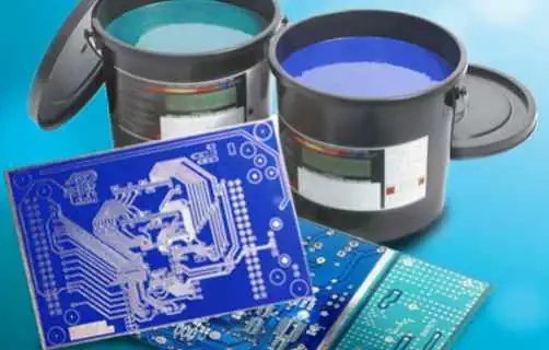
Soldermask, also known as solder resist, is a thin layer of polymer applied to the copper traces of a PCB. Its primary functions include:
  1. Protecting the copper traces from oxidation
  2. Preventing solder bridges during the assembly process
  3. Providing electrical insulation between conductors
  4. Enhancing the PCB’s aesthetic appearance

Importance of Soldermask Thickness Uniformity

The uniformity of soldermask thickness is critical for several reasons:

AspectImportancePotential Issues with Non-Uniformity
Electrical PerformanceConsistent insulation propertiesVariations in impedance, signal integrity problems
Solder Mask Dam IntegrityPrevents solder bridgingSolder bridges, short circuits
Component PlacementConsistent surface for component mountingMisalignment, poor solder joints
Visual AppearanceProfessional, high-quality lookUneven coloration, visible thickness variations
Thermal ManagementUniform heat distributionHotspots, thermal str

Silkscreen Printing Process for Soldermask Application

Overview of Silkscreen Printing

Silkscreen printing, also known as screen printing or serigraphy, is a widely used method for applying soldermask to PCBs. The process involves:

  1. Preparing a screen mesh with the desired pattern
  2. Applying soldermask ink to the screen
  3. Using a squeegee to force the ink through the screen onto the PCB
  4. Curing the applied soldermask

Key Components of Silkscreen Printing

Screen Mesh

The screen mesh is a finely woven fabric (typically made of polyester or stainless steel) stretched over a frame. Its characteristics include:

CharacteristicDescriptionImpact on Printing
Mesh CountNumber of threads per inchAffects ink deposit thickness and resolution
Thread DiameterThickness of individual threadsInfluences ink flow and print quality
Mesh TensionTightness of the mesh on the frameAffects print accuracy and consisten

Squeegee

The squeegee is a blade that moves across the screen, forcing ink through the mesh onto the PCB. Important factors include:

  1. Material (typically polyurethane or rubber)
  2. Hardness (measured in durometer)
  3. Profile (straight, beveled, or rounded edge)
  4. Pressure applied during printing

Soldermask Ink

The soldermask ink is a specially formulated polymer designed for PCB application. Key properties include:

  1. Viscosity
  2. Solid content
  3. Curing method (UV, thermal, or combination)
  4. Color and opacity

Nail-Bed Design in Silkscreen Printing

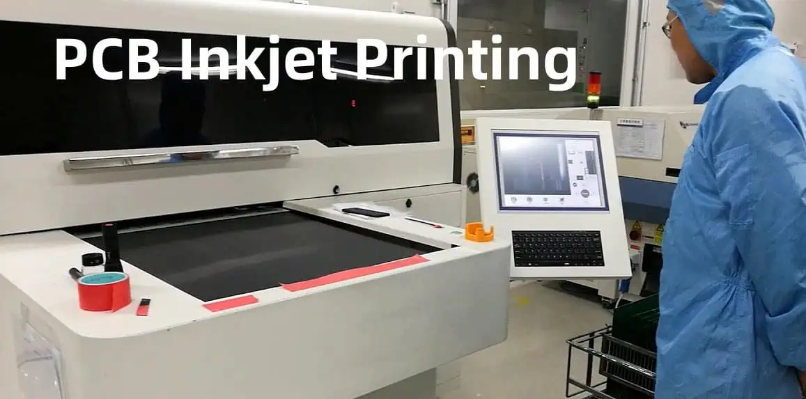
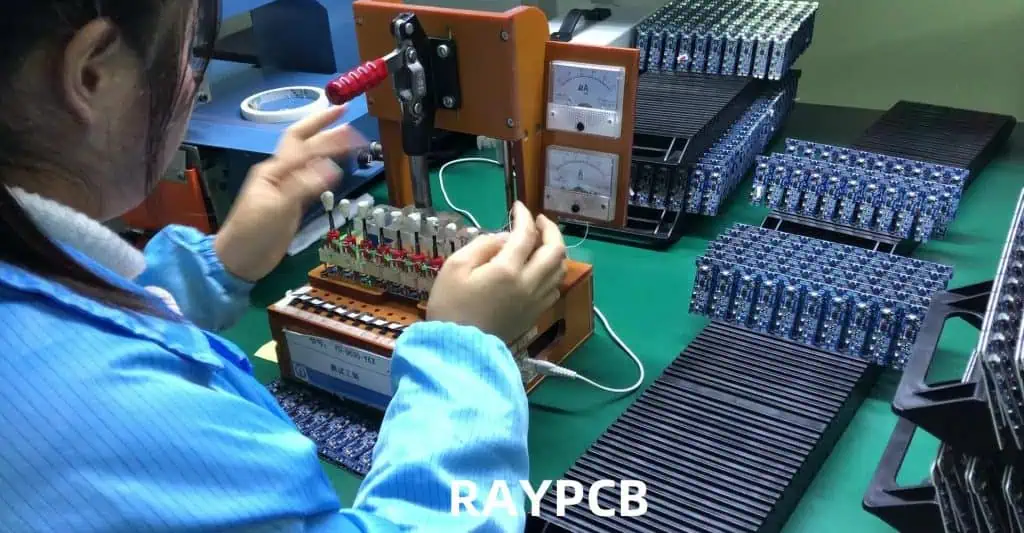
solder mask screen silk print machine
Solder mask screen silk print machine

What is a Nail-Bed Design?

The nail-bed design refers to the pattern of small, raised points or “nails” on the surface that supports the PCB during the silkscreen printing process. This design is crucial for:

  1. Minimizing contact area between the support surface and the PCB
  2. Allowing excess ink to flow away from the print area
  3. Ensuring uniform pressure distribution during printing

Key Parameters of Nail-Bed Design

ParameterDescriptionImpact on Soldermask Uniformity
Nail DensityNumber of nails per unit areaAffects support and ink flow
Nail HeightHeight of individual nailsInfluences PCB flatness during printing
Nail ShapeGeometry of nail tips (round, flat, conical)Affects contact area and pressure distribution
Nail PatternArrangement of nails (grid, offset, random)Impacts overall support and uniformit

Influence of Nail-Bed Design on Soldermask Thickness Uniformity

Pressure Distribution

The nail-bed design significantly affects the distribution of pressure during the printing process:

  1. Uniform Pressure: A well-designed nail-bed ensures even pressure across the PCB surface, promoting consistent ink deposition.
  2. Localized Pressure Points: Poorly designed nail-beds can create areas of high pressure, leading to uneven soldermask thickness.
  3. Edge Effects: The nail pattern near PCB edges can influence soldermask uniformity in these critical areas.

Ink Flow and Evacuation

The nail-bed design also impacts how excess ink flows during and after printing:

  1. Ink Channeling: Proper nail spacing allows for efficient evacuation of excess ink.
  2. Ink Pooling: Inadequate spacing can lead to ink pooling, causing thickness variations.
  3. Edge Accumulation: The nail pattern can influence ink accumulation near PCB edges.

PCB Support and Flatness

Maintaining PCB flatness during printing is crucial for uniform soldermask application:

  1. Warpage Prevention: An optimal nail-bed design helps prevent PCB warpage during printing.
  2. Consistent Gap: Proper support ensures a consistent gap between the screen and PCB surface.
  3. Thin PCB Support: The design must adequately support thin or flexible PCBs without causing deformation.

Optimizing Nail-Bed Design for Soldermask Thickness Uniformity

PCB Solder Mask

Nail Density Optimization

Finding the optimal nail density is crucial for balancing support and ink flow:

Nail DensityAdvantagesDisadvantages
High DensityBetter PCB support, reduced warpageLimited ink evacuation, potential for pressure points
Low DensityImproved ink flow and evacuationReduced support, potential for PCB deformation
Optimal DensityBalanced support and ink flowRequires careful design and testing

Recommendations for nail density optimization:

  1. Consider PCB thickness and flexibility
  2. Analyze PCB layout and component density
  3. Conduct print tests with varying nail densities
  4. Use computational fluid dynamics (CFD) simulations to predict ink flow

Nail Height and Shape Considerations

The height and shape of individual nails play a significant role in soldermask uniformity:

AspectConsiderationsImpact on Uniformity
Nail HeightMust accommodate PCB thickness variationsEnsures consistent screen-to-PCB distance
Nail Tip ShapeAffects contact area and pressure distributionInfluences local soldermask thickness
Nail ProfileCan impact ink flow around nail baseAffects evacuation of excess ink

Optimization strategies:

  1. Use adjustable-height nail-beds for different PCB thicknesses
  2. Experiment with various nail tip shapes (flat, rounded, conical)
  3. Consider tapered nail profiles to improve ink flow

Nail Pattern Design

The arrangement of nails can significantly influence soldermask uniformity:

PatternDescriptionBenefitsChallenges
GridRegular, aligned rows and columnsPredictable support, easy manufacturingPotential for regular pattern artifacts
OffsetStaggered arrangementImproved ink flow, reduced pattern effectsMore complex design and manufacturing
Variable DensityChanging density across the bedOptimized for specific PCB layouts

Optimization approaches:

  1. Analyze PCB layout to identify critical areas requiring support
  2. Use computer-aided design (CAD) tools to optimize nail patterns
  3. Consider hybrid patterns combining different arrangements

Edge Support Considerations

The nail-bed design near PCB edges requires special attention:

  1. Enhanced Edge Support: Increase nail density near edges to prevent warpage
  2. Ink Flow Management: Design channels for ink evacuation along edges
  3. Adjustable Edge Nails: Implement independently adjustable edge supports

Advanced Techniques for Nail-Bed Design Optimization

Computational Modeling and Simulation

Leveraging computational tools can significantly enhance nail-bed design:

  1. Finite Element Analysis (FEA):
    • Simulate PCB deformation under printing pressure
    • Optimize nail placement for minimal warpage
  2. Computational Fluid Dynamics (CFD):
    • Model ink flow through the nail-bed
    • Identify areas of potential ink accumulation or insufficient flow
  3. Multi-physics Simulations:
    • Combine mechanical and fluid simulations
    • Predict overall impact on soldermask thickness uniformity

Adaptive Nail-Bed Systems

Implementing adaptive systems can accommodate various PCB designs:

  1. Programmable Nail Heights:
    • Adjust individual nail heights based on PCB layout
    • Compensate for PCB thickness variations
  2. Dynamic Pressure Control:
    • Implement real-time pressure sensing and adjustment
    • Ensure uniform pressure distribution during printing
  3. Modular Nail-Bed Design:
    • Create interchangeable nail-bed sections
    • Customize support for different PCB sizes and layouts

Integration with PCB Design Process

Incorporating nail-bed considerations into the PCB design phase:

  1. Design for Manufacturability (DFM) Guidelines:
    • Develop PCB design rules that consider nail-bed support
    • Optimize component placement and copper distribution
  2. Nail-Bed Simulation in PCB Design Software:
    • Integrate nail-bed simulation tools with PCB design software
    • Predict soldermask uniformity issues during the design phase
  3. Collaborative Design Approach:
    • Foster communication between PCB designers and manufacturing engineers
    • Iteratively optimize both PCB and nail-bed designs

Measuring and Monitoring Soldermask Thickness Uniformity

PCB solder mask expose machine

Measurement Techniques

Various methods can be employed to measure soldermask thickness uniformity:

TechniqueDescriptionAdvantagesLimitations
Optical MicroscopyVisual inspection of cross-sectionsSimple, widely availableDestructive, limited sampling
X-ray Fluorescence (XRF)Non-contact measurement of thicknessNon-destructive, quickAffected by underlying materials
Eddy Current TestingMeasures thickness based on conductivityNon-destructive, fastRequires conductive substrate
3D ProfilometryCreates 3D surface mapHigh resolution, non-contactTime-consuming for large areas

Statistical Process Control (SPC)

Implementing SPC for soldermask thickness uniformity:

  1. Sampling Plans:
    • Develop appropriate sampling strategies
    • Balance between inspection thoroughness and production efficiency
  2. Control Charts:
    • Monitor thickness measurements over time
    • Identify trends and out-of-control situations
  3. Capability Analysis:
    • Calculate process capability indices (Cp, Cpk)
    • Ensure process meets specification requirements

Continuous Improvement Strategies

Leveraging measurement data for ongoing optimization:

  1. Root Cause Analysis:
    • Investigate sources of non-uniformity
    • Correlate issues with specific nail-bed design parameters
  2. Design of Experiments (DOE):
    • Systematically vary nail-bed design factors
    • Identify optimal settings for uniformity
  3. Machine Learning Approaches:
    • Develop predictive models for soldermask uniformity
    • Optimize nail-bed designs based on historical data and outcomes

Future Trends and Innovations

Advanced Materials and Processes

Emerging technologies that may impact nail-bed design and soldermask uniformity:

  1. Novel Soldermask Materials:
    • Self-leveling formulations
    • Nanotechnology-enhanced polymers
  2. Alternative Application Methods:
    • Inkjet printing of soldermask
    • Electrophoretic deposition techniques
  3. Smart Materials for Nail-Beds:
    • Shape-memory alloys for adaptive support
    • Self-cleaning surfaces to prevent ink buildup

Industry 4.0 Integration

Incorporating nail-bed optimization into the smart factory concept:

  1. Real-time Process Monitoring:
    • In-line thickness measurements
    • Adaptive control of printing parameters
  2. Digital Twin Technology:
    • Virtual modeling of the entire printing process
    • Predictive maintenance of nail-beds and printing equipment
  3. AI-Driven Optimization:
    • Machine learning algorithms for continuous process improvement
    • Automated design of optimal nail-bed configurations

Conclusion

The design of silkscreen printing nail-beds plays a crucial role in achieving uniform soldermask thickness on PCBs. By carefully considering factors such as nail density, height, shape, and pattern, manufacturers can significantly improve the quality and reliability of their products. As the electronics industry continues to demand higher performance and miniaturization, the importance of optimizing these seemingly small details becomes ever more critical.

The future of nail-bed design lies in the integration of advanced computational tools, adaptive systems, and smart manufacturing concepts. By embracing these technologies and continuously refining their processes, PCB manufacturers can ensure they meet the evolving demands of the electronics industry while maintaining the highest standards of quality and reliability.

Frequently Asked Questions (FAQ)

  1. Q: How does nail-bed design affect the overall PCB manufacturing process? A: Nail-bed design significantly impacts the silkscreen printing process, which in turn affects soldermask thickness uniformity. This uniformity is crucial for the PCB’s electrical performance, solder mask dam integrity, component placement accuracy, and overall quality. A well-designed nail-bed ensures consistent pressure distribution and proper ink flow, leading to improved manufacturing yield and product reliability.
  2. Q: What are the most critical parameters to consider when designing a nail-bed for silkscreen printing? A: The most critical parameters include:
    • Nail density: Affects support and ink flow
    • Nail height: Influences PCB flatness during printing
    • Nail shape: Impacts contact area and pressure distribution
    • Nail pattern: Affects overall support and uniformity Each of these parameters must be optimized based on the specific PCB design and manufacturing requirements.
  3. Q: How can manufacturers measure and monitor soldermask thickness uniformity effectively? A: Manufacturers can use various techniques to measure soldermask thickness uniformity:
    • Optical microscopy for visual inspection of cross-sections
    • X-ray fluorescence (XRF) for non-destructive measurements
    • Eddy current testing for quick, non-destructive assessments
    • 3D profilometry for high-resolution surface mapping Implementing statistical process control (SPC) with appropriate sampling plans and control charts is crucial for effective monitoring and continuous improvement.
  4. Q: What role does computational modeling play in nail-bed design optimization? A: Computational modeling plays a significant role in optimizing nail-bed design:
    • Finite Element Analysis (FEA) helps simulate PCB deformation under printing pressure
    • Computational Fluid Dynamics (CFD) models ink flow through the nail-bed
    • Multi-physics simulations combine mechanical and fluid simulations to predict overall impact on soldermask uniformity These tools allow designers to optimize nail-bed configurations virtually, reducing the need for extensive physical prototyping and testing.
  5. Q: How are emerging technologies and Industry 4.0 concepts influencing nail-bed design and soldermask application? A: Emerging technologies and Industry 4.0 concepts are revolutionizing nail-bed design and soldermask application:
    • Advanced materials, such as self-leveling soldermasks and smart nail-bed materials, are being developed
    • Real-time process monitoring and adaptive control systems are enabling more precise and consistent printing
    • Digital twin technology allows for virtual modeling and optimization of the entire printing process
    • AI-driven optimization techniques are being employed for continuous process improvement and automated nail-bed design These advancements are leading to more efficient, flexible, and high-quality PCB manufacturing processes.

How to Implement Quality Inspection of PCBs

Printed Circuit Boards (PCBs) are the backbone of modern electronics, serving as the foundation for countless devices we use daily. Ensuring the quality of these intricate components is crucial for the reliability and performance of electronic products. This article delves into the comprehensive process of implementing quality inspection for PCBs, covering various stages of inspection, advanced technologies, and best practices in the industry.

Understanding PCB Quality Inspection

Importance of PCB Quality Inspection

Quality inspection of PCBs is critical for several reasons:

  1. Ensuring product reliability
  2. Minimizing field failures and recalls
  3. Maintaining brand reputation
  4. Complying with industry standards and regulations
  5. Optimizing production processes

Types of PCB Defects

PCB defects can be categorized into several types:

Defect CategoryExamplesPotential Causes
Manufacturing DefectsOpen circuits, short circuits, wrong componentsProcess issues, human error
Design DefectsSignal integrity problems, thermal issuesPoor PCB layout, inadequate thermal management
Material DefectsDelamination, copper separationSubstandard materials, improper handling
Assembly DefectsSolder bridges, misaligned componentsIncorrect assembly proce

Implementing a Comprehensive PCB Inspection Process

pcb x ray inspection

Incoming Material Inspection

Raw Material Verification

  1. Base material inspection
    • Check for correct material type (e.g., FR-4, high-frequency materials)
    • Verify thickness and dielectric properties
  2. Copper foil inspection
    • Examine copper thickness and purity
    • Check for surface defects or contamination
  3. Solder mask and silkscreen material verification
    • Ensure correct color and type
    • Verify compatibility with PCB design requirements

Component Inspection

  1. Visual inspection
    • Check for physical damage or discoloration
    • Verify correct package types and markings
  2. Electrical parameter verification
    • Sample testing of critical components
    • Verification of key electrical parameters (e.g., resistance, capacitance)
  3. Documentation review
    • Check component datasheets and certificates of conformance
    • Verify compliance with RoHS and other relevant standards

Bare Board Inspection

Visual Inspection

  1. Surface examination
    • Check for scratches, dents, or other physical damage
    • Inspect solder mask and silkscreen quality
  2. Hole quality assessment
    • Examine drill hole size and position accuracy
    • Check for burrs or copper remnants in holes
  3. Copper pattern inspection
    • Verify trace width and spacing
    • Check for copper shorts or opens

Dimensional Inspection

  1. Board outline verification
    • Measure overall board dimensions
    • Check for correct profiling and edge quality
  2. Hole positioning
    • Verify hole locations against design specifications
    • Check critical hole-to-hole distances
  3. Layer alignment
    • Inspect registration between layers in multi-layer PCBs
    • Check for misalignment issues in plated through-holes

Electrical Testing

  1. Continuity and isolation testing
    • Perform automated testing to check for shorts and opens
    • Verify correct connections between pads and vias
  2. Impedance testing
  3. High-potential (Hi-Pot) testing
    • Test for dielectric strength between layers
    • Identify potential breakdown or insulation issues

PCB Assembly Inspection

Pre-Reflow Inspection

  1. Solder paste inspection (SPI)
    • Check solder paste volume and alignment
    • Identify insufficient or excessive solder paste deposits
  2. Component placement inspection
    • Verify correct component placement and orientation
    • Check for missing or misaligned components

Post-Reflow Inspection

  1. Automated Optical Inspection (AOI)
    • Inspect solder joint quality
    • Check for solder bridges, insufficient solder, or component misalignment
  2. X-ray Inspection
    • Examine hidden solder joints (e.g., BGA, QFN packages)
    • Detect voids or defects in solder connections
  3. Manual Visual Inspection
    • Perform detailed visual checks for any defects missed by automated systems
    • Inspect overall board quality and cleanliness

Functional Testing

  1. In-Circuit Testing (ICT)
    • Test individual components on the assembled PCB
    • Verify correct component values and basic functionality
  2. Boundary Scan Testing (JTAG)
    • Test interconnections between components
    • Verify functionality of complex ICs and programmable devices
  3. Functional Circuit Testing
    • Simulate real-world operating conditions
    • Verify overall PCB functionality and performance

Environmental and Reliability Testing

  1. Thermal Cycling
    • Subject PCBs to extreme temperature variations
    • Identify potential issues with solder joints or component connections
  2. Vibration Testing
    • Simulate transportation and operational vibrations
    • Verify mechanical integrity of the PCB assembly
  3. Humidity Testing
    • Expose PCBs to high humidity conditions
    • Check for potential corrosion or delamination issues

Advanced Inspection Technologies

Automated Optical Inspection (AOI)

Working Principle

AOI systems use high-resolution cameras and sophisticated image processing algorithms to inspect PCBs for defects. They compare the captured images against a “golden” reference or CAD data to identify anomalies.

Key Features

  1. High-speed inspection capabilities
  2. Detection of surface mount and through-hole defects
  3. Color analysis for solder joint quality assessment
  4. 3D measurement capabilities for component co-planarity

Inspection Parameters

ParameterDescriptionTypical Tolerance
Component PresenceVerifies if all components are present100% detection
Component OrientationChecks correct rotational alignment±5 degrees
Solder Joint QualityAssesses solder fillet shape and size±10% of ideal
Solder BridgesDetects unwanted solder connections100% detection
Component PlacementMeasures X, Y, and theta positioning±0.1mm, ±0.5 degrees

X-ray Inspection

Working Principle

FQC inspection

X-ray inspection uses high-energy radiation to penetrate through the PCB and components, creating images of internal structures. This allows for inspection of hidden solder joints and internal PCB layers.

Key Applications

  1. Inspection of Ball Grid Array (BGA) solder joints
  2. Detection of voids in solder connections
  3. Examination of internal PCB layers for defects
  4. Verification of through-hole component soldering

Inspection Capabilities

FeatureDescriptionTypical Resolution
2D X-rayProvides top-down view of PCB5-10 µm
3D X-ray (Computed Tomography)Creates 3D model of PCB internals5-20 µm
Void DetectionIdentifies and measures solder voidsDown to 2% void ratio
BGA Ball AnalysisMeasures ball size, shape, and position±1 µm accuracy

Laser-Based Inspection

Working Principle

Laser-based inspection systems use laser triangulation to create high-resolution 3D profiles of PCB surfaces. This allows for precise measurement of solder paste deposits, component heights, and coplanarity.

Key Features

  1. High-precision 3D measurements
  2. Non-contact inspection method
  3. Capability to inspect transparent or reflective surfaces
  4. Solder paste volume calculation

Inspection Parameters

ParameterDescriptionTypical Accuracy
Solder Paste HeightMeasures height of solder paste deposits±1 µm
Solder Paste VolumeCalculates volume of solder paste±3%
Component CoplanarityMeasures lead/ball heights for flatness±2 µm
Board WarpageAssesses overall PCB flatness±5 µm

Implementing an Effective PCB Inspection Strategy

Developing Inspection Criteria

  1. Review industry standards
    • IPC-A-610 for acceptability of electronic assemblies
    • IPC-6012 for rigid PCB qualification and performance specifications
  2. Analyze critical factors
    • Identify critical components and connections
    • Determine key performance parameters
  3. Establish acceptance criteria
    • Define acceptable ranges for measured parameters
    • Set pass/fail criteria for visual and functional tests

Creating Inspection Procedures

  1. Define inspection points
    • Identify key stages in the production process for inspection
    • Determine appropriate inspection methods for each stage
  2. Develop detailed work instructions
    • Create step-by-step procedures for each inspection task
    • Include visual aids and reference images
  3. Implement data collection and reporting systems
    • Define data to be collected during inspections
    • Establish reporting formats and frequency

Training and Certification

  1. Operator training
    • Provide comprehensive training on inspection equipment and procedures
    • Conduct regular refresher courses
  2. Certification programs
    • Implement internal certification processes for inspectors
    • Encourage external certifications (e.g., IPC Certification)
  3. Continuous improvement
    • Regularly assess inspector performance
    • Update training materials based on new technologies and processes

Data Analysis and Process Improvement

  1. Statistical Process Control (SPC)
    • Implement SPC techniques to monitor inspection results
    • Identify trends and potential process issues
  2. Root Cause Analysis
    • Conduct thorough investigations of recurring defects
    • Implement corrective and preventive actions
  3. Continuous process optimization
    • Use inspection data to drive process improvements
    • Regularly review and update inspection criteria and procedures

Challenges and Considerations

Balancing Inspection Thoroughness and Production Efficiency

  1. Risk-based inspection
    • Focus more rigorous inspection on critical areas or high-risk products
    • Implement sampling plans based on historical data and product criticality
  2. Inline vs. offline inspection
    • Determine optimal placement of inspection steps within the production line
    • Balance the need for 100% inspection with production speed requirements
  3. Automation vs. manual inspection
    • Evaluate the cost-effectiveness of automated inspection systems
    • Identify areas where human inspection adds significant value

Keeping Up with Technological Advancements

  1. Regular technology assessments
    • Stay informed about new inspection technologies and methodologies
    • Evaluate potential benefits of upgrading inspection systems
  2. Collaboration with equipment suppliers
    • Engage with suppliers for training and support
    • Participate in beta testing of new inspection technologies
  3. Industry networking
    • Attend conferences and trade shows focused on PCB inspection
    • Participate in industry working groups and standards committees

Managing Inspection Data

  1. Data storage and retrieval
    • Implement robust systems for storing inspection data
    • Ensure easy accessibility for analysis and traceability
  2. Data security
    • Protect sensitive inspection data and intellectual property
    • Comply with data protection regulations
  3. Integration with MES and ERP systems
    • Connect inspection data with broader manufacturing and business systems
    • Enable real-time decision making based on inspection results

Future Trends in PCB Inspection

Artificial Intelligence and Machine Learning

  1. Defect classification and prediction
    • Use AI algorithms to improve defect detection accuracy
    • Implement predictive maintenance for inspection equipment
  2. Adaptive inspection
    • Develop systems that can adjust inspection parameters based on historical data
    • Implement self-learning algorithms for continual improvement

Industry 4.0 Integration

  1. IoT-enabled inspection equipment
    • Connect inspection systems to the broader factory network
    • Enable real-time monitoring and control of inspection processes
  2. Digital twin technology
    • Create virtual models of PCBs for enhanced defect analysis
    • Simulate inspection processes for optimization

Advanced Imaging Technologies

  1. Terahertz imaging
    • Explore non-destructive testing methods for internal PCB structures
    • Improve detection of hidden defects in multi-layer PCBs
  2. Hyperspectral imaging
    • Enhance material analysis capabilities
    • Improve detection of contamination and material defects

Conclusion

Implementing a comprehensive quality inspection process for PCBs is crucial for ensuring the reliability and performance of electronic products. By combining visual, automated, and functional inspection methods, manufacturers can detect a wide range of defects and maintain high-quality standards. As technology continues to advance, staying up-to-date with the latest inspection techniques and equipment will be essential for remaining competitive in the PCB manufacturing industry.

Effective PCB inspection requires a holistic approach, integrating advanced technologies with well-defined procedures, trained personnel, and continuous improvement processes. By focusing on these elements and adapting to new challenges and technologies, PCB manufacturers can ensure the highest levels of quality and reliability in their products.

Frequently Asked Questions (FAQ)

  1. Q: What is the most critical stage of PCB inspection? A: While all stages are important, the post-reflow inspection is often considered the most critical. This stage, which typically includes AOI and X-ray inspection, can detect a wide range of assembly defects such as solder joint issues, component misalignment, and hidden defects in BGA packages.
  2. Q: How does automated inspection compare to manual inspection? A: Automated inspection systems like AOI and AXI offer high-speed, consistent, and objective inspection capabilities, making them ideal for high-volume production. Manual inspection, while slower, can be more flexible and better at detecting certain types of defects that require human judgment. A combination of both methods is often the most effective approach.
  3. Q: What are the key factors to consider when choosing PCB inspection equipment? A: Key factors include the types of PCBs being produced (e.g., complexity, size), production volume, required inspection speed, types of defects to be detected, integration with existing systems, and overall cost-effectiveness. It’s also important to consider the equipment’s ease of use, reliability, and the availability of technical support.
  4. Q: How often should inspection criteria and procedures be updated? A: Inspection criteria and procedures should be reviewed and updated regularly, typically at least annually or whenever there are significant changes in product design, manufacturing processes, or industry standards. Additionally, they should be reviewed after any major quality issues or customer complaints to ensure continuous improvement.
  5. Q: What role does data analysis play in PCB inspection? A: Data analysis is crucial in PCB inspection for several reasons:
    • Identifying trends and patterns in defects
    • Optimizing inspection processes and parameters
    • Driving continuous improvement in manufacturing processes
    • Enabling predictive maintenance of inspection equipment
    • Supporting traceability and compliance requirements By effectively analyzing inspection data, manufacturers can proactively address quality issues and improve overall production efficiency.

Methods Contributing to Optimization of LED PCB Design and Quality Control

Light Emitting Diode (LED) technology has revolutionized the lighting industry, offering energy-efficient and long-lasting solutions for various applications. The heart of any LED-based product lies in its Printed Circuit Board (PCB) design. Optimizing LED PCB design and implementing rigorous quality control measures are crucial for ensuring the performance, reliability, and longevity of LED products. This article delves into the methods that contribute to the optimization of LED PCB design and quality control, providing insights for manufacturers, engineers, and quality assurance professionals in the LED industry.

Understanding LED PCB Basics

What is an LED PCB?

An LED PCB is a specialized circuit board designed to support and power Light Emitting Diodes. These PCBs are engineered to provide optimal electrical, thermal, and mechanical performance for LED applications. They differ from standard PCBs in several ways:

  1. Enhanced thermal management capabilities
  2. Specialized copper patterns for current distribution
  3. Reflective surfaces for improved light output
  4. Customized layouts for specific LED arrangements

Types of LED PCBs

LED PCBs come in various types, each suited for different applications and performance requirements:

PCB TypeDescriptionAdvantagesCommon Applications
FR-4Standard fiberglass-based PCBCost-effective, widely availableLow-power LED applications
Aluminum PCB (MCPCB)PCB with aluminum base for heat dissipationExcellent thermal managementHigh-power LED lighting
Ceramic PCBMade from ceramic materialsSuperior thermal performance, high frequency capabilityAutomotive lighting, high-reliability applications
Flexible PCBBendable PCB made from flexible materialsConformable to various s

Optimization Techniques for LED PCB Design

Thermal Management Strategies

Effective thermal management is crucial for LED PCB performance and longevity. Here are some key strategies:

Heat Dissipation Design

  1. Thermal vias: Implement an array of thermal vias beneath LED components to efficiently transfer heat from the top layer to the bottom layer or internal heat-spreading planes.
  2. Copper pour: Maximize copper area on all layers to improve heat spreading and dissipation.
  3. Thermal pads: Design larger thermal pads for LED components to enhance heat transfer to the PCB.

Material Selection

Choose PCB materials with high thermal conductivity:

MaterialThermal Conductivity (W/mK)Advantages
FR-40.25 – 0.5Cost-effective, suitable for low-power applications
Aluminum PCB1.0 – 3.0Excellent heat dissipation, ideal for high-power LEDs
Ceramic PCB20 – 170Superior thermal performance, suitable for extr

Thermal Simulation and Analysis

Utilize thermal simulation software to:

  • Identify hotspots on the PCB
  • Optimize component placement for better heat distribution
  • Validate thermal design before production

Electrical Design Considerations

Current Distribution

  1. Trace width calculation: Use appropriate trace widths to handle the required current without excessive voltage drop or heat generation.
  2. Power planes: Implement dedicated power planes for high-current applications to ensure uniform current distribution.
  3. Star topology: Arrange LED connections in a star topology to maintain consistent voltage across all LEDs.

EMI/EMC Optimization

  1. Ground plane design: Use a solid ground plane to minimize electromagnetic interference (EMI) and improve signal integrity.
  2. Component placement: Keep high-frequency components and sensitive signal traces away from power circuits to reduce EMI.
  3. Filtering: Implement proper filtering techniques, such as decoupling capacitors and ferrite beads, to suppress noise and EMI.

Optical Performance Enhancement

Reflective Surfaces

  1. White solder mask: Use white solder mask on the LED side of the PCB to increase reflectivity and improve light output.
  2. Reflective coatings: Apply specialized reflective coatings to enhance light reflection and overall efficiency.

LED Placement and Spacing

  1. Uniform distribution: Ensure uniform spacing between LEDs to achieve consistent light output and avoid hotspots.
  2. Angle consideration: Adjust LED placement angles to optimize light distribution for specific applications.

Advanced PCB Design Techniques

Multi-layer PCB Design

Multi-layer PCB designs offer several advantages for complex LED applications:

  1. Improved thermal management: Dedicated internal layers for heat spreading.
  2. Enhanced signal integrity: Separation of power and signal layers.
  3. Increased functionality: More space for additional components and features.

Design considerations for multi-layer LED PCBs:

  • Use internal layers for power distribution and heat spreading
  • Implement proper layer stackup for optimal performance
  • Utilize blind and buried vias for compact designs

Flexible and Rigid-Flex PCB Design

Flexible and rigid-flex PCBs enable unique LED applications:

  1. Curved surfaces: Conform to non-planar surfaces for architectural lighting.
  2. Dynamic lighting: Create movable or foldable LED displays.
  3. Space-saving designs: Fit LED circuits into compact or irregularly shaped spaces.

Key considerations:

  • Choose appropriate flexible materials with good thermal properties
  • Design for stress relief in bent areas
  • Implement proper layer transitions between rigid and flexible sections

High-Frequency PCB Design for LED Drivers

Modern LED drivers often operate at high frequencies, requiring special PCB design techniques:

  1. Controlled impedance: Design traces with specific impedance for high-frequency signals.
  2. Signal integrity: Minimize crosstalk and reflections through proper trace routing and termination.
  3. EMI suppression: Implement advanced EMI suppression techniques such as guard traces and stitching vias.

Quality Control Measures for LED PCBs

Incoming Material Inspection

Implement rigorous inspection processes for incoming materials:

  1. PCB substrate: Check for defects, proper thickness, and material composition.
  2. Components: Verify authenticity, specifications, and condition of LEDs and other components.
  3. Solder paste and flux: Ensure proper composition and storage conditions.

In-Process Quality Control

Monitor and control critical parameters during the PCB assembly process:

Solder Paste Inspection (SPI)

Inspection ParameterAcceptable RangePotential Issues if Out of Range
Paste volume±20% of nominalInsufficient solder joints, tombstoning
Paste alignment±50% of pad areaSolder bridges, open circuits
Paste height±25% of stencil thicknessWeak solder joints, component misalignme

Automated Optical Inspection (AOI)

Implement AOI at various stages of the assembly process:

  1. Pre-reflow: Verify component placement and orientation.
  2. Post-reflow: Inspect solder joint quality and component presence.
  3. Final inspection: Check for overall PCB quality and cleanliness.

X-ray Inspection

Use X-ray inspection for:

  1. Detecting voids in solder joints, especially for bottom-terminated components.
  2. Inspecting hidden solder joints in multi-layer or double-sided PCBs.
  3. Verifying internal layer connections and via structures.

Functional Testing

Develop comprehensive functional test procedures:

  1. Electrical testing: Verify correct voltages, currents, and LED functionality.
  2. Thermal testing: Conduct thermal imaging to identify hotspots and verify thermal design.
  3. Optical testing: Measure light output, color consistency, and beam patterns.
  4. Environmental testing: Subject PCBs to temperature cycling, humidity, and vibration tests to ensure reliability.

Reliability Testing and Analysis

Implement long-term reliability testing:

  1. Accelerated life testing: Subject LEDs to elevated temperatures and currents to predict long-term performance.
  2. Thermal cycling: Expose PCBs to extreme temperature variations to test for thermal stress resistance.
  3. Failure analysis: Conduct root cause analysis on any failures to improve design and processes.

Emerging Technologies and Future Trends

Advanced Materials

  1. Graphene-based PCBs: Explore the potential of graphene for improved thermal conductivity and electrical performance.
  2. Nano-ceramic composites: Investigate new ceramic composites for enhanced thermal management in high-power applications.

Intelligent PCB Design

  1. AI-assisted design: Utilize artificial intelligence algorithms for optimizing PCB layouts and thermal management.
  2. Digital twins: Implement digital twin technology for real-time monitoring and predictive maintenance of LED PCBs.

Integration of IoT and Smart Lighting

  1. Embedded sensors: Integrate environmental and occupancy sensors directly into LED PCBs for smart lighting applications.
  2. Wireless connectivity: Incorporate low-power wireless modules for IoT-enabled lighting control and monitoring.

Conclusion

Optimizing LED PCB design and quality control is a multifaceted process that requires careful consideration of thermal, electrical, and optical factors. By implementing advanced design techniques, rigorous quality control measures, and staying abreast of emerging technologies, manufacturers can produce high-performance, reliable LED PCBs that meet the demanding requirements of modern lighting applications.

As the LED industry continues to evolve, the integration of new materials, intelligent design processes, and IoT capabilities will further enhance the functionality and efficiency of LED PCBs. Staying informed about these advancements and continuously refining design and quality control processes will be crucial for success in the competitive LED market.

Frequently Asked Questions (FAQ)

  1. Q: What is the most critical factor in LED PCB design? A: While all aspects are important, thermal management is often considered the most critical factor in LED PCB design. Effective heat dissipation is essential for maintaining LED performance, color stability, and longevity.
  2. Q: How does the choice of PCB material affect LED performance? A: PCB material significantly impacts thermal management and, consequently, LED performance. Materials with higher thermal conductivity, such as aluminum or ceramic, allow for better heat dissipation, which can lead to improved LED efficiency and lifespan.
  3. Q: What are the advantages of using multi-layer PCBs for LED applications? A: Multi-layer PCBs offer improved thermal management through dedicated heat-spreading layers, enhanced signal integrity by separating power and signal layers, and increased functionality by providing more space for additional components and features.
  4. Q: How important is automated inspection in LED PCB quality control? A: Automated inspection, including SPI, AOI, and X-ray inspection, is crucial for maintaining high quality in LED PCB production. These technologies can detect defects that are difficult or impossible to spot with manual inspection, ensuring consistent product quality and reliability.
  5. Q: What emerging technologies are likely to impact LED PCB design in the near future? A: Key emerging technologies include advanced materials like graphene-based PCBs, AI-assisted design for optimization, digital twin technology for real-time monitoring, and the integration of IoT capabilities for smart lighting applications. These technologies have the potential to significantly enhance LED PCB performance, efficiency, and functionality.

How to Design Embedded Resistors in PCB?

Printed Circuit Boards (PCBs) are the backbone of modern electronics, providing a compact and efficient platform for mounting and interconnecting electronic components. As technology advances and the demand for miniaturization grows, designers are constantly seeking innovative ways to optimize PCB designs. One such innovation is the use of embedded resistors, which offer numerous advantages over traditional surface-mount resistors.

This comprehensive guide will explore the world of embedded resistors in PCB design, covering everything from the basics to advanced techniques and considerations. We’ll delve into the benefits, design process, materials, manufacturing techniques, and best practices for incorporating embedded resistors into your PCB designs.

Understanding Embedded Resistors

What Are Embedded Resistors?

Embedded resistors are resistive elements that are integrated directly into the inner layers of a PCB, rather than being mounted on the surface. These resistors are formed using specialized resistive materials and manufacturing processes, becoming an integral part of the PCB structure.

Advantages of Embedded Resistors

Embedded resistors offer several significant advantages over traditional surface-mount resistors:

  1. Space-saving: By integrating resistors into the PCB layers, valuable surface area is freed up for other components or routing.
  2. Improved reliability: Embedded resistors are protected from environmental factors and mechanical stress, leading to increased durability.
  3. Enhanced electrical performance: Shorter connection paths reduce parasitic effects and improve signal integrity.
  4. Cost-effective for high-volume production: While initial setup costs may be higher, embedded resistors can be more economical in large-scale manufacturing.
  5. Improved thermal management: Embedded resistors distribute heat more evenly throughout the PCB.

Types of Embedded Resistors

There are several types of embedded resistors, each with its own characteristics and applications:

  1. Printed Resistors: Created by printing resistive ink or paste onto the PCB substrate.
  2. Plated Resistors: Formed by electroplating a resistive material onto the PCB.
  3. Thin-film Resistors: Deposited as a thin film of resistive material on the PCB surface.
  4. Thick-film Resistors: Similar to thin-film, but with a thicker layer of resistive material.

Designing Embedded Resistors

Design Considerations

When incorporating embedded resistors into your PCB design, several factors must be considered:

  1. Resistance value and tolerance
  2. Power dissipation
  3. Temperature coefficient of resistance (TCR)
  4. Frequency response
  5. Current-carrying capacity
  6. Available PCB real estate
  7. Manufacturing process compatibility

Design Process

The process of designing embedded resistors typically involves the following steps:

  1. Determine resistor requirements
  2. Select appropriate resistive material
  3. Calculate resistor dimensions
  4. Choose resistor location within PCB layers
  5. Design resistor terminations
  6. Verify design using simulation tools
  7. Create necessary documentation for manufacturing

Let’s explore each of these steps in detail.

1. Determine Resistor Requirements

Begin by clearly defining the electrical specifications for each embedded resistor:

  • Resistance value and tolerance
  • Maximum power dissipation
  • Operating temperature range
  • Frequency range (if applicable)
  • Current rating

2. Select Appropriate Resistive Material

Choose a resistive material that best meets your design requirements. Common materials include:

MaterialSheet Resistance Range (Ω/sq)TCR (ppm/°C)Typical Tolerance
NiCr10 – 1000±50 to ±100±5% to ±10%
TaN10 – 1000±25 to ±50±1% to ±5%
RuO210 – 10000±50 to ±200±5% to ±20%
Carbon10 – 1000000-200 to -600±10% to ±30%

3. Calculate Resistor Dimensions

SMD Resistor

Use the following formula to determine the dimensions of your embedded resistor:

R = (ρ * L) / (W * T)

Where:

  • R: Resistance value (Ω)
  • ρ: Resistivity of the material (Ω·m)
  • L: Length of the resistor (m)
  • W: Width of the resistor (m)
  • T: Thickness of the resistive layer (m)

Adjust the length and width to achieve the desired resistance value while considering manufacturing limitations and available space.

4. Choose Resistor Location

Determine the optimal location for each embedded resistor within the PCB stack-up. Consider factors such as:

  • Proximity to associated components
  • Thermal management
  • Signal integrity
  • Layer availability

5. Design Resistor Terminations

Create appropriate terminations for the embedded resistors to ensure proper electrical connection and mechanical stability. Common termination methods include:

6. Verify Design Using Simulation Tools

Use PCB design and simulation software to verify the performance of your embedded resistors. Key aspects to simulate include:

  • DC and AC performance
  • Thermal behavior
  • Signal integrity
  • Electromagnetic compatibility (EMC)

7. Create Manufacturing Documentation

Prepare detailed documentation for the PCB manufacturer, including:

  • PCB stack-up information
  • Resistor material specifications
  • Resistor dimensions and locations
  • Termination details
  • Test and verification requirements

Manufacturing Techniques for Embedded Resistors

Printed Resistor Process

  1. Screen printing: Resistive ink is applied through a patterned screen onto the PCB substrate.
  2. Photolithography: A photosensitive resistive material is applied, exposed, and developed to create the resistor pattern.

Plated Resistor Process

  1. Subtractive process: A resistive layer is plated over the entire board, then selectively etched to form resistors.
  2. Additive process: Resistive material is selectively plated onto pre-defined areas of the PCB.

Thin-film and Thick-film Processes

  1. Sputtering: Resistive material is deposited onto the PCB substrate using physical vapor deposition.
  2. Chemical vapor deposition (CVD): Resistive material is formed on the PCB through chemical reactions in a vapor phase.

Best Practices for Embedded Resistor Design

  1. Start with larger tolerances: Begin your design with wider tolerance ranges and tighten them as necessary during prototyping and testing.
  2. Consider thermal management: Design your PCB layout to efficiently dissipate heat generated by embedded resistors.
  3. Use standardized values: Whenever possible, use standard resistance values to simplify manufacturing and reduce costs.
  4. Implement proper terminations: Ensure that resistor terminations are designed for reliability and ease of testing.
  5. Account for parasitic effects: Consider the impact of parasitic capacitance and inductance when designing high-frequency circuits.
  6. Utilize design rules: Implement and follow design rules specific to embedded resistors to ensure manufacturability and reliability.
  7. Plan for testing and verification: Design your PCB with test points or structures that allow for easy verification of embedded resistor values.

Challenges and Limitations

While embedded resistors offer numerous advantages, they also come with some challenges and limitations:

  1. Limited resistance range: The available resistance values are typically more limited compared to discrete resistors.
  2. Trimming requirements: Some embedded resistors may require laser trimming to achieve precise resistance values, adding complexity to the manufacturing process.
  3. Design flexibility: Once embedded, resistors cannot be easily modified or replaced, limiting design flexibility.
  4. Initial cost: The setup and tooling costs for embedded resistor manufacturing can be higher than those for traditional surface-mount resistors.
  5. Thermal considerations: Heat dissipation can be more challenging with embedded resistors, requiring careful thermal management in high-power designs.

Future Trends in Embedded Resistor Technology

As PCB technology continues to evolve, several trends are emerging in the field of embedded resistors:

  1. Improved materials: Development of new resistive materials with better stability, lower TCR, and wider resistance ranges.
  2. Enhanced manufacturing processes: Advancements in printing and deposition technologies for more precise and reliable embedded resistors.
  3. Integration with other passive components: Combining embedded resistors with capacitors and inductors to create fully integrated passive networks.
  4. 3D printing: Exploration of additive manufacturing techniques for creating complex embedded resistor structures.
  5. Smart PCBs: Integration of embedded resistors with sensors and microcontrollers for self-monitoring and adaptive functionality.

Conclusion

Embedded resistors represent a significant advancement in PCB design, offering numerous benefits in terms of space savings, reliability, and performance. By understanding the design process, manufacturing techniques, and best practices outlined in this guide, PCB designers can effectively incorporate embedded resistors into their designs, pushing the boundaries of miniaturization and functionality in electronic devices.

As technology continues to evolve, embedded resistors will likely play an increasingly important role in the future of electronics, enabling more compact, efficient, and reliable designs across a wide range of applications.

Frequently Asked Questions (FAQ)

1. What is the typical tolerance range for embedded resistors?

Embedded resistors typically have tolerances ranging from ±1% to ±20%, depending on the material and manufacturing process used. Printed and plated resistors often have wider tolerances (±5% to ±20%), while thin-film resistors can achieve tighter tolerances (±1% to ±5%). It’s important to note that tighter tolerances generally come with higher manufacturing costs.

2. How do I choose between embedded resistors and surface-mount resistors for my PCB design?

The choice between embedded and surface-mount resistors depends on several factors:

  • Space constraints: If board real estate is at a premium, embedded resistors can free up valuable surface area.
  • Production volume: For high-volume production, embedded resistors can be more cost-effective despite higher initial setup costs.
  • Electrical performance: If your design requires minimal parasitic effects or improved signal integrity, embedded resistors may be preferable.
  • Design flexibility: If you anticipate frequent design changes or need the ability to easily replace components, surface-mount resistors offer greater flexibility.
  • Resistance value range: If you need a wide range of precise resistance values, surface-mount resistors may be more suitable.

Consider these factors in the context of your specific design requirements to make the best choice.

3. Can embedded resistors be used in high-frequency applications?

Yes, embedded resistors can be used in high-frequency applications and often offer better performance than surface-mount resistors due to reduced parasitic effects. However, proper design considerations are crucial:

  • Use materials with low dielectric loss for the PCB substrate.
  • Minimize the length of resistor terminations to reduce inductance.
  • Consider the skin effect at high frequencies when calculating resistor dimensions.
  • Use electromagnetic simulation tools to verify performance and optimize layouts for high-frequency operation.

4. What are the key challenges in testing and verifying embedded resistors?

Testing and verifying embedded resistors can be challenging due to their integration within the PCB layers. Key challenges include:

  1. Limited physical access: Traditional probing methods may not be possible.
  2. Influence of surrounding circuitry: Adjacent traces and components can affect measurements.
  3. Accuracy of test equipment: High-precision equipment may be required for tight-tolerance resistors.
  4. Temperature effects: Thermal considerations during testing can impact resistance measurements.

To address these challenges, consider implementing dedicated test structures, using flying probe testers, or employing built-in self-test (BIST) circuitry in your design.

5. How do embedded resistors impact the overall reliability of a PCB?

Embedded resistors generally improve the overall reliability of a PCB in several ways:

  1. Protection from environmental factors: Being embedded within the PCB layers shields the resistors from moisture, dust, and other contaminants.
  2. Reduced mechanical stress: Embedded resistors are less susceptible to vibration and shock compared to surface-mounted components.
  3. Improved thermal management: Heat dissipation is more evenly distributed throughout the PCB.
  4. Fewer solder joints: Reducing the number of solder connections decreases potential failure points.
  5. Consistent performance: Embedded resistors maintain more stable characteristics over time due to their protected environment.

However, it’s important to note that proper design and manufacturing processes are crucial to realizing these reliability benefits. Poorly designed or manufactured embedded resistors can potentially lead to difficult-to-diagnose failures within the PCB structure.

Streamline Assembly and Improve Reliability with Flexible and Flex-rigid PCBs

In the ever-evolving world of electronics, the demand for smaller, lighter, and more reliable devices continues to grow. As a result, manufacturers are constantly seeking innovative solutions to meet these challenges. One such solution that has gained significant traction in recent years is the use of flexible and flex-rigid printed circuit boards (PCBs). These advanced PCB technologies offer a range of benefits that can streamline assembly processes and improve overall product reliability.

This comprehensive article will delve into the world of flexible and flex-rigid PCBs, exploring their characteristics, advantages, applications, and the impact they have on assembly processes and product reliability. We’ll also discuss design considerations, manufacturing techniques, and future trends in this exciting field of electronics.

Understanding Flexible and Flex-rigid PCBs

What are Flexible PCBs?

Flexible PCBs, also known as flex circuits, are thin, bendable circuit boards made from flexible materials such as polyimide or polyester. These boards can be bent, folded, or shaped to fit into tight spaces or conform to irregular surfaces. Unlike traditional rigid PCBs, flexible PCBs offer a level of versatility that opens up new possibilities in product design and functionality.

What are Flex-rigid PCBs?

Flex-rigid PCBs combine the best of both worlds by integrating flexible and rigid board technologies into a single circuit board. These hybrid designs typically consist of multiple layers of flexible circuits bonded to rigid board sections. This unique construction allows for complex circuit designs that can bend in specific areas while maintaining rigidity where needed.

Key Differences Between Flexible and Flex-rigid PCBs

To better understand the distinctions between flexible and flex-rigid PCBs, let’s compare their key characteristics:

CharacteristicFlexible PCBsFlex-rigid PCBs
CompositionSingle or multi-layer flexible materialsCombination of flexible and rigid materials
FlexibilityEntirely flexibleFlexible in specific areas, rigid in others
ThicknessTypically thinnerGenerally thicker due to rigid sections
ComplexitySimpler designsCan accommodate more complex designs
CostGenerally lowerUsually higher due to complex manufacturing
ApplicationsWearables, mobile devicesAerospace, medical devices, automotive

Advantages of Flexible and Flex-rigid PCBs

Space and Weight Savings

One of the primary advantages of flexible and flex-rigid PCBs is their ability to save space and reduce weight in electronic devices. These boards can be bent, folded, or shaped to fit into tight or irregularly shaped spaces, allowing for more compact and lightweight designs. This is particularly beneficial in industries such as aerospace, wearable technology, and mobile devices, where every gram and millimeter counts.

Improved Reliability

Flexible and flex-rigid PCBs offer enhanced reliability compared to traditional rigid boards in several ways:

  1. Resistance to vibration and shock: The flexible nature of these boards allows them to absorb vibrations and shocks more effectively, reducing the risk of component failure or solder joint fractures.
  2. Reduced connector count: By eliminating the need for multiple rigid boards connected by cables or connectors, flex and flex-rigid designs reduce potential points of failure.
  3. Better thermal management: Flexible materials can dissipate heat more efficiently, helping to prevent thermal stress and extend the lifespan of components.
  4. Resistance to flexing fatigue: High-quality flexible materials can withstand repeated bending and flexing without degradation, ensuring long-term reliability in dynamic applications.

Simplified Assembly Process

The use of flexible and flex-rigid PCBs can significantly streamline the assembly process:

  1. Reduced part count: By integrating multiple boards into a single flexible or flex-rigid design, manufacturers can reduce the number of separate components that need to be assembled.
  2. Elimination of connectors and cables: Flex circuits can replace traditional wire harnesses and connectors, simplifying assembly and reducing the potential for human error.
  3. 3D design capabilities: Flex-rigid boards can be designed to fit precisely into three-dimensional spaces, reducing the need for complex assembly procedures.
  4. Automated assembly compatibility: Many flexible and flex-rigid PCBs are compatible with automated assembly processes, further streamlining production.

Enhanced Design Freedom

Flexible and flex-rigid PCBs offer designers greater freedom to create innovative and efficient product layouts:

  1. Conforming to unique form factors: These boards can be shaped to fit around obstacles or conform to curved surfaces, enabling more creative product designs.
  2. Dynamic applications: Flexible circuits can be used in applications that require movement, such as folding smartphones or rotating camera modules.
  3. Improved signal integrity: By reducing the need for long traces and interconnects, flex and flex-rigid designs can improve signal integrity and reduce electromagnetic interference.

Applications of Flexible and Flex-rigid PCBs

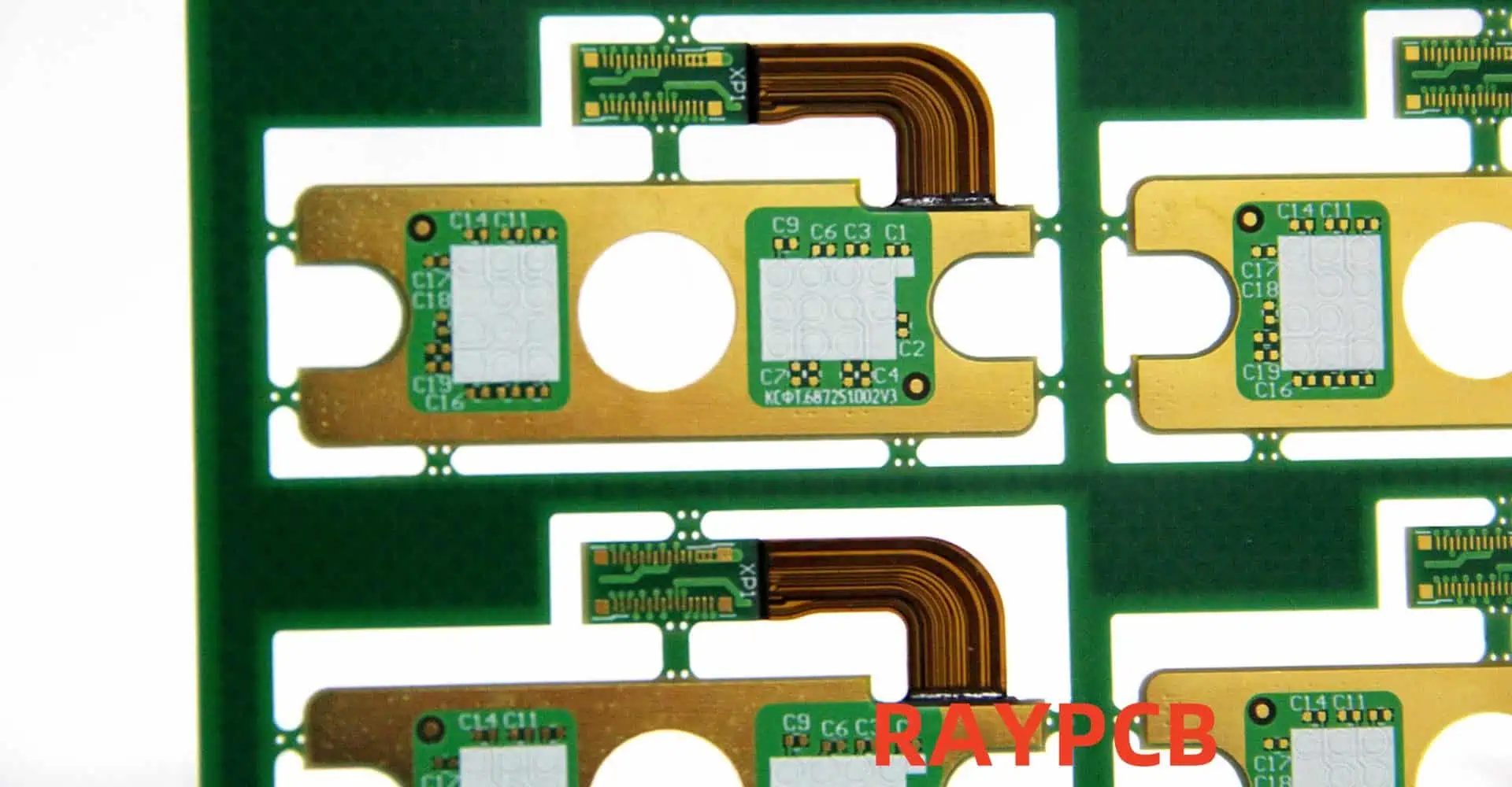
rigid-flex pcb
rigid-flex pcb

The versatility of flexible and flex-rigid PCBs has led to their adoption across a wide range of industries and applications:

Consumer Electronics

  1. Smartphones and tablets
  2. Wearable devices (smartwatches, fitness trackers)
  3. Digital cameras and camcorders
  4. Laptop computers and e-readers

Automotive Industry

  1. Dashboard displays and control panels
  2. Advanced driver assistance systems (ADAS)
  3. Engine control modules
  4. LED lighting systems

Aerospace and Defense

  1. Satellite systems
  2. Aircraft avionics
  3. Missile guidance systems
  4. Radar and communication equipment

Medical Devices

  1. Implantable medical devices
  2. Hearing aids
  3. Portable diagnostic equipment
  4. Surgical robots

Industrial Applications

  1. Robotics and automation systems
  2. Smart sensors and IoT devices
  3. Handheld test and measurement equipment
  4. 3D printers

Design Considerations for Flexible and Flex-rigid PCBs

Designing flexible and flex-rigid PCBs requires careful consideration of several factors to ensure optimal performance and reliability:

Material Selection

Choosing the right materials is crucial for the success of flexible and flex-rigid PCB designs:

Material TypeCommon OptionsConsiderations
Base materialPolyimide, PolyesterTemperature resistance, flexibility, cost
ConductorCopper, AluminumConductivity, weight, cost
AdhesivesAcrylic, EpoxyBond strength, flexibility, thermal properties
Coverlay/Solder maskPolyimide, LPIProtection, flexibility, ease of application

Bend Radius and Flex Zones

When designing flexible sections, it’s essential to consider the minimum bend radius to prevent damage to the circuit:

  1. Calculate the minimum bend radius based on the material thickness and copper weight.
  2. Design flex zones with gradual transitions to distribute stress evenly.
  3. Avoid placing components or vias in areas subject to frequent bending.

Component Placement

Proper component placement is critical for the reliability of flexible and flex-rigid PCBs:

  1. Place components on rigid sections when possible to reduce stress on solder joints.
  2. If components must be placed on flexible areas, use appropriate stiffeners or support structures.
  3. Consider the direction of board flexing when orienting components.

Layer Stack-up Design

The layer stack-up in flex-rigid PCBs requires careful planning:

  1. Balance the number of layers in rigid and flexible sections to minimize overall thickness.
  2. Use symmetrical designs to prevent warping during manufacturing.
  3. Consider impedance control requirements when designing the stack-up.

Trace Routing

Proper trace routing is essential for maintaining signal integrity and reliability:

  1. Use rounded corners for traces in flexible areas to reduce stress concentrations.
  2. Route traces perpendicular to bend lines when possible.
  3. Utilize hatched ground planes in flexible sections to improve flexibility.

Manufacturing Processes for Flexible and Flex-rigid PCBs

The manufacturing of flexible and flex-rigid PCBs involves several specialized processes:

Flexible PCB Manufacturing

  1. Material preparation: Cutting and cleaning of base materials.
  2. Imaging and etching: Creating circuit patterns using photolithography and chemical etching.
  3. Coverlay application: Applying protective layers to exposed circuits.
  4. Final processing: Cutting, drilling, and shaping the flexible circuit.

Flex-rigid PCB Manufacturing

  1. Layer fabrication: Creating individual flexible and rigid layers.
  2. Lamination: Bonding flexible and rigid layers together under heat and pressure.
  3. Drilling and plating: Creating through-holes and vias to connect layers.
  4. Outer layer processing: Imaging, etching, and finishing of outer layers.
  5. Final processing: Cutting, shaping, and testing the completed flex-rigid board.

Quality Control and Testing

Ensuring the quality and reliability of flexible and flex-rigid PCBs requires rigorous testing:

  1. Visual inspection: Checking for defects in circuit patterns and materials.
  2. Electrical testing: Verifying continuity and insulation resistance.
  3. Bend testing: Ensuring flexibility and durability of flex sections.
  4. Environmental testing: Subjecting boards to temperature, humidity, and vibration tests.

Future Trends in Flexible and Flex-rigid PCB Technology

The field of flexible and flex-rigid PCBs continues to evolve, with several exciting trends on the horizon:

  1. Stretchable electronics: Development of PCBs that can not only bend but also stretch, opening up new possibilities in wearable technology and soft robotics.
  2. Advanced materials: Research into new flexible substrate materials with improved thermal, electrical, and mechanical properties.
  3. Additive manufacturing: Exploration of 3D printing techniques for creating flexible and flex-rigid PCBs, potentially revolutionizing prototyping and small-scale production.
  4. Integration with other technologies: Combining flexible PCBs with technologies such as printed electronics and embedded components to create highly integrated and compact devices.
  5. Sustainability: Development of eco-friendly materials and manufacturing processes to reduce the environmental impact of flexible and flex-rigid PCB production.

Conclusion

Flexible and flex-rigid PCBs represent a significant advancement in electronic design and manufacturing. By offering space and weight savings, improved reliability, simplified assembly processes, and enhanced design freedom, these innovative circuit board technologies are enabling the creation of smaller, lighter, and more reliable electronic devices across a wide range of industries.

As the demand for compact, high-performance electronics continues to grow, the importance of flexible and flex-rigid PCBs is likely to increase. Designers and manufacturers who embrace these technologies and master their unique design and production challenges will be well-positioned to create the next generation of innovative electronic products.

By streamlining assembly processes and improving overall product reliability, flexible and flex-rigid PCBs are not just a trend but a fundamental shift in how we approach electronic design. As the technology continues to evolve, we can expect to see even more exciting applications and advancements in this dynamic field.

Frequently Asked Questions (FAQ)

  1. Q: What are the main differences between flexible and flex-rigid PCBs? A: Flexible PCBs are entirely bendable and made from flexible materials, while flex-rigid PCBs combine flexible and rigid sections in a single board. Flex-rigid PCBs offer more design complexity and can accommodate a wider range of components, but are generally more expensive to produce than fully flexible PCBs.
  2. Q: Are flexible and flex-rigid PCBs more expensive than traditional rigid PCBs? A: Generally, yes. The specialized materials and manufacturing processes required for flexible and flex-rigid PCBs typically result in higher costs compared to traditional rigid PCBs. However, these costs can often be offset by the benefits they offer, such as space savings, reduced assembly complexity, and improved reliability.
  3. Q: How do I determine if my project would benefit from using a flexible or flex-rigid PCB? A: Consider using flexible or flex-rigid PCBs if your project requires: fitting electronics into tight or irregularly shaped spaces, reducing weight, improving reliability in high-vibration environments, or simplifying complex interconnections between multiple boards. They are particularly beneficial in applications such as wearables, mobile devices, aerospace, and medical equipment.
  4. Q: What are the key design considerations for flexible and flex-rigid PCBs? A: Important design considerations include: selecting appropriate materials, calculating minimum bend radii, designing proper flex zones, careful component placement, optimizing layer stack-up, and implementing specialized trace routing techniques. It’s also crucial to consider manufacturing processes and testing requirements early in the design phase.
  5. Q: How long do flexible and flex-rigid PCBs last compared to rigid PCBs? A: When properly designed and manufactured, flexible and flex-rigid PCBs can offer comparable or even superior lifespan to rigid PCBs. Their ability to withstand repeated flexing and better resistance to vibration and shock can contribute to improved longevity in many applications. However, the exact lifespan depends on factors such as the specific materials used, environmental conditions, and the frequency and degree of flexing in the application.

Stencil Design Requirement on QFN Components for Optimal Performance of PCBA

In the world of printed circuit board assembly (PCBA), the quest for miniaturization and improved performance has led to the widespread adoption of Quad Flat No-lead (QFN) components. These compact, surface-mount devices offer excellent electrical and thermal performance, making them a popular choice in various electronic applications. However, the successful implementation of QFN components heavily relies on precise solder paste deposition, which is primarily achieved through stencil design.

This comprehensive guide delves into the intricacies of stencil design requirements for QFN components, exploring how optimal stencil design can significantly enhance the performance and reliability of PCBAs. We’ll cover everything from the basics of QFN packages and stencil printing to advanced design considerations and troubleshooting techniques.

Understanding QFN Components

QFN Component Mounting

What are QFN Components?

Quad Flat No-lead (QFN) components are a type of surface-mount device characterized by their compact size, excellent thermal performance, and lack of protruding leads. Instead of traditional leads, QFN packages have a planar copper lead frame that terminates at the bottom edge of the package, forming electrical connections when soldered to the PCB.

Advantages of QFN Components

QFN components offer several benefits that make them increasingly popular in modern electronics:

  1. Smaller footprint and lower profile
  2. Improved electrical performance due to shorter connection paths
  3. Enhanced thermal performance through exposed pad
  4. Reduced parasitic effects
  5. Cost-effective manufacturing

Challenges in QFN Assembly

Despite their advantages, QFN components present unique challenges in the assembly process:

  1. Difficulty in visual inspection of solder joints
  2. Potential for solder bridging between closely spaced pads
  3. Risk of insufficient solder on corner pads
  4. Voiding in the thermal pad area
  5. Sensitivity to moisture and handling

The Importance of Stencil Design in QFN Assembly

Role of Stencil Printing

Stencil printing is a critical step in the surface mount technology (SMT) process, responsible for depositing precise amounts of solder paste onto the PCB pads. For QFN components, accurate solder paste deposition is crucial for:

  1. Ensuring proper electrical connections
  2. Achieving optimal thermal performance
  3. Preventing solder defects such as bridging or insufficient solder
  4. Controlling voiding in the thermal pad area

Impact of Stencil Design on PCBA Performance

The stencil design directly influences the quality and reliability of the solder joints in QFN components. Proper stencil design can:

  1. Improve first-pass yield rates
  2. Enhance long-term reliability of the assembly
  3. Optimize thermal management
  4. Reduce rework and associated costs
  5. Ensure consistent electrical performance

Key Considerations in Stencil Design for QFN Components

Stencil Thickness

The thickness of the stencil plays a crucial role in determining the volume of solder paste deposited. For QFN components, consider the following:

  • Typical stencil thickness ranges from 3 to 5 mils (0.076 to 0.127 mm)
  • Thinner stencils (3-4 mils) are often used for fine-pitch QFNs
  • Thicker stencils (4-5 mils) may be necessary for larger thermal pads

Aperture Design

Aperture design is critical for achieving the right solder paste volume and distribution. Key aspects include:

  1. Aperture size
  2. Aperture shape
  3. Area ratio
  4. Aspect ratio

Aperture Size

For QFN perimeter pads:

  • Typically 1:1 ratio with pad size
  • May be slightly reduced (80-90% of pad width) for fine-pitch QFNs

For thermal pads:

  • Usually divided into smaller apertures
  • Total aperture area typically 50-80% of the thermal pad area

Aperture Shape

  • Rectangular apertures for perimeter pads
  • Various shapes for thermal pad apertures (e.g., square, circular, or cross-shaped)

Area Ratio

Area ratio is the ratio of the aperture opening area to the aperture wall area. For reliable paste release:

  • Aim for an area ratio ≥ 0.66 for square apertures
  • Aim for an area ratio ≥ 0.60 for circular apertures

Aspect Ratio

Aspect ratio is the ratio of the aperture width to the stencil thickness. For optimal performance:

  • Maintain an aspect ratio ≥ 1.5 for square apertures
  • Maintain an aspect ratio ≥ 1.8 for circular apertures

Thermal Pad Considerations

The thermal pad (exposed pad) of QFN components requires special attention in stencil design:

  1. Use multiple smaller apertures instead of a single large aperture
  2. Implement a “window pane” or gridded pattern
  3. Consider the use of “home plate” shaped apertures for corner coverage
  4. Adjust aperture sizes to control solder paste volume and voiding

Stencil Design Strategies for Different QFN Package Types

Fine-Pitch QFNs

For QFN packages with pitches below 0.5 mm:

  • Use thinner stencils (3-4 mils)
  • Reduce aperture width to 80-90% of pad width
  • Consider stepped stencils for simultaneous fine-pitch and standard components

Large Thermal Pad QFNs

For QFNs with large thermal pads:

  • Implement gridded aperture patterns
  • Adjust aperture sizes to achieve 50-80% solder paste coverage
  • Consider multi-level stencils for balanced paste deposition

Mixed-Technology Boards

When assembling boards with QFNs and other component types:

  • Use step stencils to accommodate different paste volume requirements
  • Consider multi-level stencils for complex mixed-technology designs
  • Optimize aperture designs for each component type

Advanced Stencil Design Techniques

Stepped Stencils

Stepped stencils feature areas of different thicknesses, allowing for:

  • Optimized paste volumes for different component types
  • Improved solder paste release for fine-pitch QFNs
  • Enhanced control over thermal pad solder volume

Multi-Level Stencils

Multi-level stencils offer even greater flexibility:

  • Multiple thickness levels for complex mixed-technology boards
  • Precise control over solder paste volume for various component types
  • Improved first-pass yield rates in challenging designs

Nano-Coated Stencils

Nano-coated stencils feature a special surface treatment that:

  • Enhances solder paste release, especially for fine-pitch applications
  • Improves print definition and consistency
  • Extends stencil life and reduces cleaning frequency

Stencil Material Selection

The choice of stencil material can significantly impact printing performance:

MaterialCharacteristicsBest For
Stainless SteelDurable, cost-effectiveGeneral purpose, high-volume production
NickelSmoother aperture walls, better releaseFine-pitch applications, challenging designs
Electroformed NickelExtremely smooth aperture walls, excellent releaseUltra-fine-pitch, critical applications
Laser-Cut PolyimideFlexible, suitable for step stencilsPrototyping, low-volu

Optimizing Stencil Design for QFN Components

Design Rules and Best Practices

  1. Maintain consistent aperture sizes for perimeter pads
  2. Use area and aspect ratio guidelines to ensure reliable paste release
  3. Implement gridded patterns for thermal pad apertures
  4. Consider component proximity and adjust apertures accordingly
  5. Use corner apertures or “home plate” designs for improved corner coverage
  6. Validate designs through simulation and testing

Simulation and Modeling

Utilize advanced simulation tools to:

  • Predict solder paste behavior
  • Optimize aperture designs
  • Identify potential issues before production

Design for Manufacturing (DFM) Considerations

  1. Collaborate with your stencil manufacturer and assembly partner
  2. Consider the capabilities and limitations of available printing equipment
  3. Design for easy stencil cleaning and maintenance
  4. Implement fiducial marks for accurate stencil alignment

Troubleshooting Common QFN Stencil Printing Issues

IssuePossible CausesSolutions
Insufficient SolderUndersized apertures, poor paste releaseIncrease aperture size, adjust stencil thickness, consider nano-coating
Solder BridgingOversized apertures, excessive pasteReduce aperture size, optimize stencil thickness, improve printer setup
Corner LiftingInsufficient corner solderImplement corner apertures, use “home plate” designs
Excessive VoidingImproper thermal pad aperture designAdjust gridded pattern, optimize aperture sizes
Inconsistent PrintingStencil flexing, poor gasketingUse tensioned stencils, improve

Future Trends in QFN Stencil Design

As technology continues to evolve, several trends are emerging in QFN stencil design:

  1. Integration of artificial intelligence for optimized aperture designs
  2. Advanced materials for improved paste release and durability
  3. 3D-printed stencils for rapid prototyping and small-batch production
  4. Enhanced simulation tools for more accurate prediction of solder paste behavior
  5. Automated stencil design systems integrated with PCB design software

Conclusion

Stencil design plays a crucial role in the successful assembly of QFN components, directly impacting the performance, reliability, and yield of PCBAs. By understanding the key considerations, implementing advanced design techniques, and following best practices, engineers and designers can optimize their stencil designs for QFN components, ensuring high-quality assemblies that meet the demanding requirements of modern electronics.

As QFN packages continue to evolve and miniaturize, the importance of precise stencil design will only grow. Staying informed about the latest techniques, materials, and technologies in stencil design will be essential for maintaining a competitive edge in the rapidly advancing field of electronics manufacturing.

Frequently Asked Questions (FAQ)

1. What is the optimal stencil thickness for QFN components?

The optimal stencil thickness for QFN components typically ranges from 3 to 5 mils (0.076 to 0.127 mm). The specific thickness depends on several factors:

  • QFN pitch: Fine-pitch QFNs (< 0.5 mm) often require thinner stencils (3-4 mils) for better control of solder paste volume.
  • Thermal pad size: Larger thermal pads may benefit from thicker stencils (4-5 mils) to ensure sufficient solder paste volume.
  • Mixed-technology boards: When assembling boards with various component types, a compromise thickness or step stencil may be necessary.

It’s important to balance the stencil thickness with aperture design to achieve optimal area and aspect ratios for reliable paste release.

2. How do I determine the appropriate aperture design for the thermal pad of a QFN?

Designing apertures for QFN thermal pads involves several considerations:

  1. Coverage area: Aim for 50-80% solder paste coverage of the total thermal pad area.
  2. Pattern: Use a gridded or “window pane” pattern rather than a single large aperture.
  3. Aperture shape: Consider square, circular, or cross-shaped apertures.
  4. Size distribution: Implement smaller apertures around the edges and larger ones in the center to promote outgassing.
  5. Corner coverage: Use “home plate” shaped apertures in the corners for better solder distribution.

Start with a standard pattern and adjust based on assembly results and thermal requirements. Simulation tools can help optimize the design before production.

3. What are the main differences in stencil design for fine-pitch QFNs compared to standard QFNs?

Stencil design for fine-pitch QFNs (typically < 0.5 mm pitch) requires special considerations:

  1. Thinner stencils: Usually 3-4 mils thick for better control of solder paste volume.
  2. Reduced aperture width: Often 80-90% of the pad width to prevent solder bridging.
  3. Stricter area and aspect ratios: More critical for ensuring reliable paste release.
  4. Nano-coatings: May be beneficial for improving paste release in challenging fine-pitch designs.
  5. Step stencils: Consider using step stencils when fine-pitch QFNs are combined with other component types on the same board.

These adjustments help manage the smaller solder paste volumes required for fine-pitch QFNs while maintaining reliable connections and preventing defects.

4. How can I minimize voiding in QFN thermal pads through stencil design?

Minimizing voiding in QFN thermal pads through stencil design involves several strategies:

  1. Optimize aperture pattern: Use a gridded pattern with spaces between apertures to allow for outgassing.
  2. Adjust aperture sizes: Implement smaller apertures around the edges and larger ones in the center to promote outward flow of volatiles.
  3. Control solder paste volume: Aim for 50-80% coverage of the thermal pad area to balance thermal performance and void reduction.
  4. Consider aperture shapes: Experiment with circular or cross-shaped apertures, which can promote better outgassing.
  5. Implement corner apertures: Use “home plate” shaped apertures in the corners to ensure good coverage while allowing gas escape paths.
  6. Fine-tune through testing: Adjust your design based on X-ray inspection results and thermal performance testing.

Remember that while stencil design is crucial, other factors like solder paste formulation, reflow profile, and PCB surface finish also play important roles in void reduction.

5. What are the advantages of using step stencils for QFN assembly?

Step stencils offer several advantages for QFN assembly, especially in mixed-technology boards:

  1. Optimized paste volumes: Different thicknesses can be used for various component types, ensuring appropriate solder paste volume for each.
  2. Improved fine-pitch printing: Thinner sections can be used for fine-pitch QFNs while maintaining thicker areas for standard components.
  3. Enhanced thermal pad control: Stepped areas can provide better control over solder paste volume for QFN thermal pads.
  4. Reduced need for compromise: Instead of choosing a single thickness that’s a compromise for all components, step stencils allow optimization for each area.
  5. Improved first-pass yield: By providing optimal solder paste volumes for different component types, step stencils can reduce assembly defects and improve overall yield.
  6. Cost-effective solution: While more expensive than standard stencils, step stencils can be more cost-effective than using multiple stencils or dealing with high rework rates.

When designing a step stencil, work closely with your stencil manufacturer to ensure the design is within their manufacturing capabilities and compatible with your printing equipment.

What is Buried Capacitance PCB?

Printed Circuit Boards (PCBs) are the backbone of modern electronics, providing a sturdy foundation for components and facilitating electrical connections between them. As electronic devices become increasingly complex and compact, PCB designers are constantly seeking innovative ways to optimize board performance and space utilization. One such innovation that has gained significant traction in recent years is the concept of Buried Capacitance PCB.

In this comprehensive article, we will delve deep into the world of Buried Capacitance PCB technology, exploring its definition, principles, advantages, challenges, and applications. We’ll also discuss how this technology compares to traditional PCB designs and examine its impact on the electronics industry as a whole.

Understanding Buried Capacitance PCB

Definition and Basic Concept

Buried Capacitance PCB, also known as embedded capacitance or power-ground laminate technology, is an advanced PCB design technique that integrates capacitance directly into the board structure. This is achieved by creating an extremely thin dielectric layer between power and ground planes within the PCB stack-up.

The fundamental principle behind buried capacitance is based on the basic formula for capacitance:

CopyC = ε * A / d

Where:

  • C is the capacitance
  • ε is the dielectric constant of the material
  • A is the area of the conductive plates
  • d is the distance between the plates

By minimizing the distance between power and ground planes and using materials with high dielectric constants, PCB designers can create significant capacitance within the board itself.

Historical Context

The concept of buried capacitance in PCBs emerged in the late 1990s as a response to the increasing challenges posed by high-speed digital circuits. As clock speeds and edge rates increased, traditional discrete decoupling capacitors began to show limitations in their ability to suppress noise and maintain power integrity.

The development of buried capacitance technology was driven by the need for:

  1. Improved power distribution
  2. Enhanced signal integrity
  3. Reduced electromagnetic interference (EMI)
  4. More efficient use of PCB real estate

Over the years, the technology has evolved and matured, finding applications in various industries, from consumer electronics to aerospace and defense.

How Buried Capacitance PCB Works

Physical Structure

A typical buried capacitance PCB incorporates the following key elements:

  1. Power plane
  2. Ultra-thin dielectric layer (usually less than 10 μm)
  3. Ground plane

These layers are typically placed near the center of the PCB stack-up, surrounded by signal layers and additional power/ground planes as needed.

Electrical Characteristics

The buried capacitance structure exhibits several important electrical characteristics:

  1. Low inductance: Due to the extremely short current path between power and ground planes, the inductance is significantly reduced compared to discrete capacitors.
  2. Distributed capacitance: The capacitance is spread evenly across the entire board area, providing more uniform decoupling.
  3. High-frequency performance: The low inductance and distributed nature of buried capacitance make it effective at suppressing high-frequency noise.
  4. Reduced impedance: The power distribution network (PDN) impedance is lowered, improving overall system performance.

Comparison with Traditional Decoupling Methods

To better understand the advantages of buried capacitance, let’s compare it with traditional decoupling methods:

CharacteristicTraditional DecouplingBuried Capacitance
Component CountHigh (many discrete capacitors)Low (integrated into PCB)
Board SpaceSignificant space requiredMinimal impact on board space
Effectiveness at High FrequenciesLimited by parasitic inductanceHighly effective
Uniformity of DecouplingLocalizedDistributed across the board
Design ComplexityCan be complex (placement optimization)Simplified design process
CostVariable (depends on component count)Higher initial cost, po

Advantages of Buried Capacitance PCB

Improved Signal Integrity

One of the primary benefits of buried capacitance PCB is the significant improvement in signal integrity. This is achieved through:

  1. Reduced ground bounce: The low-impedance power distribution network minimizes voltage fluctuations.
  2. Decreased crosstalk: The tighter coupling between power and ground planes reduces electromagnetic interference between signal traces.
  3. Better return path: The continuous ground plane provides an optimal return path for high-speed signals.

Enhanced Power Integrity

Buried capacitance technology offers several advantages for power integrity:

  1. Lower PDN impedance: The distributed capacitance reduces the overall impedance of the power distribution network.
  2. Improved transient response: The low-inductance path between power and ground planes allows for faster charge delivery to switching components.
  3. Reduced voltage ripple: The integrated decoupling helps maintain a more stable supply voltage across the board.

Space Savings and Component Reduction

By integrating capacitance into the PCB structure, designers can:

  1. Eliminate or reduce the number of surface-mounted decoupling capacitors.
  2. Free up valuable board space for additional components or further miniaturization.
  3. Simplify the PCB assembly process by reducing the number of components to be placed.

EMI Reduction

Buried capacitance PCBs contribute to reduced electromagnetic interference (EMI) through:

  1. Lower ground plane impedance, which minimizes common-mode radiation.
  2. Reduced current loop areas, decreasing the antenna effect of PCB traces.
  3. Improved shielding effectiveness due to the tightly coupled power and ground planes.

Reliability Improvements

The use of buried capacitance can enhance overall system reliability:

  1. Fewer solder joints: With fewer discrete components, there are fewer potential points of failure.
  2. Reduced thermal stress: The elimination of surface-mounted capacitors can lead to more even heat distribution.
  3. Improved resistance to mechanical stress: The integrated nature of buried capacitance makes it less susceptible to vibration and shock.

Design Considerations for Buried Capacitance PCB

Material Selection

Choosing the right materials is crucial for effective buried capacitance implementation:

  1. Dielectric material: High-k materials are preferred to maximize capacitance.
  2. Copper foil: Ultra-thin copper foils are often used to minimize the distance between planes.
  3. Prepreg and core materials: These must be compatible with the thin dielectric and copper layers.

Stack-up Design

Careful consideration of the PCB stack-up is essential:

  1. Placement of buried capacitance layers: Typically near the center of the stack-up for optimal performance.
  2. Signal layer arrangement: Proper distribution of signal layers around the buried capacitance structure.
  3. Impedance control: Adjusting trace widths and spacings to maintain desired impedances.

Power Plane Design

Effective power plane design is critical for maximizing the benefits of buried capacitance:

  1. Partitioning: Separating different voltage domains while maintaining capacitive coupling.
  2. Void management: Minimizing voids in the power plane to ensure uniform capacitance.
  3. Current capacity: Ensuring sufficient copper weight to handle the required current.

Simulation and Modeling

Advanced simulation tools are often necessary to optimize buried capacitance designs:

  1. 3D electromagnetic simulation: For accurate modeling of the complex PCB structure.
  2. Power integrity analysis: To verify PDN performance and identify potential issues.
  3. Signal integrity simulation: To ensure that high-speed signals maintain their integrity.

Challenges and Limitations

Manufacturing Complexities

Buried capacitance PCBs present several manufacturing challenges:

  1. Thin material handling: Working with ultra-thin dielectrics requires specialized equipment and processes.
  2. Registration accuracy: Precise alignment of layers is crucial for consistent capacitance.
  3. Yield considerations: The complexity of the process can lead to lower yields, especially in early implementations.

Cost Considerations

While buried capacitance can offer long-term cost benefits, there are initial cost hurdles:

  1. Higher material costs: Specialized materials for buried capacitance are often more expensive.
  2. Increased manufacturing costs: The complex process and potential for lower yields can drive up production costs.
  3. Design costs: Additional time and expertise required for optimizing buried capacitance designs.

Design Tool Limitations

Many existing PCB design tools may not fully support buried capacitance technology:

  1. Stack-up definition: Some tools may struggle with ultra-thin layers in the stack-up.
  2. Capacitance calculation: Accurate modeling of distributed capacitance can be challenging.
  3. Design rule checking: Specialized rules for buried capacitance may not be readily available.

Performance Limitations

While buried capacitance offers many advantages, it’s not a universal solution:

  1. Frequency limitations: There’s an upper limit to the frequency range where buried capacitance is effective.
  2. Capacitance density: The achievable capacitance per unit area may be lower than with some discrete components.
  3. Voltage limitations: The thin dielectric layers may limit the maximum operating voltage.

Applications of Buried Capacitance PCB

High-Speed Digital Systems

Buried capacitance technology finds extensive use in high-speed digital applications:

  1. Servers and data centers: Where signal integrity and power distribution are critical.
  2. Telecommunications equipment: For handling high-speed data transmission.
  3. High-performance computing: To support the demands of advanced processors and memory systems.

RF and Microwave Circuits

The low-inductance characteristics of buried capacitance make it valuable in RF applications:

  1. Wireless communication devices: For improved signal quality and reduced interference.
  2. Radar systems: To enhance sensitivity and reduce noise.
  3. Satellite communications: Where space and weight savings are crucial.

Aerospace and Defense

The reliability and performance benefits of buried capacitance are particularly valuable in aerospace:

  1. Avionics systems: For enhanced reliability in critical flight control systems.
  2. Satellite electronics: Where size, weight, and power (SWaP) optimization is essential.
  3. Military communications: For improved EMI resistance and signal security.

Consumer Electronics

As consumer devices become more compact and powerful, buried capacitance offers advantages:

  1. Smartphones and tablets: Enabling more features in smaller form factors.
  2. Wearable devices: Where space savings and power efficiency are paramount.
  3. High-end audio equipment: For improved signal purity and noise reduction.

Automotive Electronics

The automotive industry is increasingly adopting buried capacitance technology:

  1. Advanced driver assistance systems (ADAS): For reliable, high-speed signal processing.
  2. Infotainment systems: To manage complex multimedia and connectivity features.
  3. Electric vehicle control systems: For efficient power management and noise reduction.

Future Trends and Developments

Material Advancements

Ongoing research in materials science is likely to yield improvements:

  1. Higher-k dielectrics: To achieve greater capacitance density.
  2. Thinner and more robust materials: For improved performance and manufacturability.
  3. Novel composite materials: Combining electrical and thermal management properties.

Integration with Other Technologies

Buried capacitance is likely to be combined with other advanced PCB technologies:

  1. Embedded active and passive components: Further miniaturization and performance improvements.
  2. 3D printed electronics: Potential for customized, high-performance buried capacitance structures.
  3. Flexible and stretchable electronics: Adapting buried capacitance concepts to non-rigid substrates.

Design Tool Evolution

PCB design software is expected to evolve to better support buried capacitance:

  1. Improved simulation capabilities: More accurate modeling of distributed capacitance effects.
  2. Automated optimization: Tools to help designers maximize the benefits of buried capacitance.
  3. Integration with AI and machine learning: For more efficient and effective PCB designs.

Standardization Efforts

As the technology matures, we can expect to see:

  1. Industry standards: Defining best practices for buried capacitance implementation.
  2. Testing and qualification procedures: Ensuring reliability and performance consistency.
  3. Design guidelines: Helping engineers effectively incorporate buried capacitance in their designs.

Conclusion

Buried Capacitance PCB technology represents a significant advancement in the field of electronic design, offering a range of benefits including improved signal and power integrity, space savings, and enhanced reliability. While it presents some challenges in terms of manufacturing complexity and initial costs, the advantages it offers make it an increasingly attractive option for a wide range of applications.

As the technology continues to evolve and mature, we can expect to see even greater adoption across various industries, from consumer electronics to aerospace and defense. The ongoing developments in materials science, design tools, and manufacturing processes will likely address many of the current limitations, further expanding the potential of buried capacitance PCB technology.

For engineers and PCB designers, understanding and leveraging buried capacitance technology will be crucial in creating the next generation of high-performance, compact, and reliable electronic systems. As we move towards an increasingly connected and digital world, the role of advanced PCB technologies like buried capacitance will only grow in importance, enabling the innovative devices and systems that will shape our future.

Frequently Asked Questions (FAQ)

1. What is the main difference between buried capacitance and traditional decoupling methods?

The main difference lies in how capacitance is implemented. Traditional decoupling methods use discrete capacitors soldered onto the PCB surface, while buried capacitance integrates the capacitance directly into the PCB structure using extremely thin dielectric layers between power and ground planes. This results in distributed, low-inductance capacitance that is effective at higher frequencies and doesn’t consume valuable board space.

2. Is buried capacitance PCB technology suitable for all types of electronic designs?

While buried capacitance offers significant advantages, it’s not necessarily suitable or cost-effective for all designs. It’s most beneficial in high-speed digital systems, RF applications, and designs where space is at a premium. For simpler, low-speed designs or where cost is the primary concern, traditional PCB designs with discrete components may still be more appropriate.

3. How does buried capacitance PCB affect the overall cost of a product?

The cost impact of buried capacitance PCB is complex. Initially, it may increase costs due to more expensive materials and manufacturing processes. However, it can lead to cost savings in other areas, such as reduced component count, simplified assembly, and improved reliability. The overall cost-effectiveness depends on the specific application, production volume, and long-term reliability requirements.

4. Can buried capacitance completely eliminate the need for discrete decoupling capacitors?

In most cases, buried capacitance significantly reduces the need for discrete decoupling capacitors but doesn’t entirely eliminate it. Some designs may still require a few strategically placed discrete capacitors to handle specific frequency ranges or provide localized decoupling for sensitive components. The exact balance depends on the specific design requirements and performance goals.

5. What are the key challenges in manufacturing buried capacitance PCBs?

The main challenges in manufacturing buried capacitance PCBs include:

  1. Handling and processing ultra-thin dielectric materials
  2. Achieving precise registration and alignment of layers
  3. Maintaining consistent quality and yield, especially for large board sizes
  4. Managing the increased complexity of the PCB stack-up
  5. Implementing effective testing and quality control procedures for the buried capacitance structure

These challenges require specialized equipment, expertise, and careful process control to overcome.

Elements Ensuring Your First-Time Success in New Product Introduction (NPI) during Electronic Manufacturing

In the fast-paced world of electronic manufacturing, bringing a new product to market successfully is a complex and challenging process. New Product Introduction (NPI) is a critical phase that can make or break the success of your product. It’s the bridge between product development and full-scale production, requiring careful planning, execution, and coordination across multiple disciplines.

This comprehensive guide will explore the key elements that ensure first-time success in NPI during electronic manufacturing. We’ll delve into the crucial steps, best practices, and strategies that can help you navigate this intricate process with confidence and efficiency.

Understanding New Product Introduction (NPI)

Definition and Scope

New Product Introduction (NPI) is the complete process of bringing a new product from concept to market. In the context of electronic manufacturing, it encompasses all the steps necessary to transform a design into a manufacturable, high-quality product that can be produced at scale.

The Importance of NPI in Electronic Manufacturing

NPI plays a pivotal role in the success of any new electronic product. It’s during this phase that potential issues are identified and resolved, manufacturing processes are optimized, and the groundwork for efficient, high-quality production is laid. A well-executed NPI process can:

  1. Reduce time-to-market
  2. Minimize production costs
  3. Ensure product quality and reliability
  4. Improve manufacturing efficiency
  5. Enhance customer satisfaction

Phases of NPI

The NPI process typically consists of several distinct phases:

  1. Concept Development
  2. Design and Engineering
  3. Prototype assembly board Development
  4. Design Validation and Testing
  5. Process Development
  6. Pilot Production
  7. Ramp to Volume Production

Each phase builds upon the previous one, creating a structured approach to bringing a new product to market.

Key Elements for NPI Success

Electronic Devices Manufacturing

1. Robust Design for Manufacturability (DFM)

Design for Manufacturability is a crucial element in ensuring NPI success. It involves designing the product with manufacturing considerations in mind from the outset.

Principles of DFM

  • Simplify the design
  • Use standard components where possible
  • Design for easy assembly
  • Consider tolerances and manufacturing variability
  • Minimize the number of parts

Benefits of DFM in NPI

  1. Reduced manufacturing costs
  2. Improved product quality
  3. Faster time-to-market
  4. Enhanced reliability
  5. Easier maintenance and repair

DFM Checklist for Electronic Products

Design Aspect Consideration
PCB Layout Adequate spacing between components
Component Selection Use of readily available, standard parts
Thermal Management Proper heat dissipation design
Testability Inclusion of test points and debug interfaces
Assembly Minimize manual assembly steps

2. Comprehensive Design Verification and Validation

Thorough design verification and validation are essential to catch and resolve issues early in the NPI process.

Types of Design Verification

  1. Functional Testing
  2. Environmental Testing
  3. Reliability Testing
  4. Safety Testing
  5. Electromagnetic Compatibility (EMC) Testing

Importance of Early Validation

  • Identifies design flaws before production
  • Reduces costly redesigns
  • Ensures compliance with industry standards
  • Validates product performance under various conditions

Best Practices for Design Verification

  1. Develop a comprehensive test plan
  2. Use simulation tools for early verification
  3. Conduct thorough prototype testing
  4. Involve manufacturing engineers in the validation process
  5. Document and analyze all test results

3. Effective Supply Chain Management

A well-managed supply chain is critical for successful NPI in electronic manufacturing.

Key Aspects of Supply Chain Management in NPI

  1. Supplier Selection and Qualification
  2. Component Sourcing and Management
  3. Inventory Planning
  4. Logistics and Transportation
  5. Risk Management

Strategies for Optimizing the Supply Chain

  • Develop strong supplier relationships
  • Implement multi-sourcing strategies for critical components
  • Use advanced forecasting techniques
  • Leverage technology for supply chain visibility
  • Establish clear communication channels with suppliers

Supply Chain Risk Mitigation Table

Risk Factor Mitigation Strategy
Component Obsolescence Regular BOM reviews, lifetime buys
Supply Disruptions Multi-sourcing, buffer inventory
Quality Issues Supplier audits, incoming quality control
Lead Time Variations Safety stock, flexible production planning
Cost Fluctuations Long-term contracts, hedging strategies

4. Robust Process Development and Optimization

Developing and optimizing manufacturing processes is crucial for ensuring consistent quality and efficiency in production.

Key Elements of Process Development

  1. Manufacturing Process Design
  2. Equipment Selection and Setup
  3. Process Parameter Optimization
  4. Work Instructions and Standard Operating Procedures (SOPs)
  5. Quality Control Measures

Techniques for Process Optimization

  • Statistical Process Control (SPC)
  • Design of Experiments (DOE)
  • Lean Manufacturing Principles
  • Six Sigma Methodology
  • Continuous Improvement Programs

Benefits of Process Optimization in NPI

  1. Improved product quality
  2. Increased production efficiency
  3. Reduced manufacturing costs
  4. Enhanced process consistency
  5. Faster problem resolution

5. Comprehensive Documentation and Change Management

Proper documentation and change management are essential for maintaining control and traceability throughout the NPI process.

Types of Critical Documentation in NPI

  1. Bill of Materials (BOM)
  2. Assembly Drawings and Instructions
  3. Test Procedures and Specifications
  4. Process Flow Charts
  5. Quality Control Plans
  6. Engineering Change Orders (ECOs)

Importance of Effective Change Management

  • Ensures all stakeholders are aware of design or process changes
  • Maintains product consistency and quality
  • Facilitates regulatory compliance
  • Enables efficient problem-solving and continuous improvement

Best Practices for Documentation and Change Management

  1. Implement a robust document control system
  2. Establish clear change request and approval processes
  3. Maintain version control for all documents
  4. Ensure accessibility of documentation to relevant team members
  5. Regularly review and update documentation

6. Cross-Functional Team Collaboration

Successful NPI requires seamless collaboration between various departments and disciplines.

Key Teams Involved in NPI

  1. Research and Development
  2. Engineering (Electrical, Mechanical, Software)
  3. Manufacturing
  4. Quality Assurance
  5. Supply Chain Management
  6. Marketing and Sales

Strategies for Effective Collaboration

  • Establish clear roles and responsibilities
  • Implement regular cross-functional meetings
  • Use collaborative tools and platforms
  • Encourage open communication and feedback
  • Align team goals and incentives

Benefits of Strong Cross-Functional Collaboration

  1. Faster decision-making
  2. Improved problem-solving
  3. Enhanced innovation
  4. Reduced time-to-market
  5. Better alignment between product design and manufacturing capabilities

7. Advanced Quality Planning and Control

Implementing robust quality planning and control measures is crucial for ensuring product reliability and customer satisfaction.

Elements of Quality Planning in NPI

  1. Failure Mode and Effects Analysis (FMEA)
  2. Control Plans
  3. Measurement System Analysis (MSA)
  4. Process Capability Studies
  5. Quality Function Deployment (QFD)

Quality Control Techniques

  • In-Process Quality Checks
  • Final Product Testing
  • Statistical Quality Control
  • Automated Optical Inspection (AOI)
  • X-ray Inspection for PCB Assemblies

Quality Metrics for NPI Success

Metric Description
First Pass Yield (FPY) Percentage of units passing all tests without rework
Defects Per Million Opportunities (DPMO) Number of defects per million chances for a defect
Customer Returns Rate Percentage of products returned by customers
On-Time Delivery Percentage of orders delivered on schedule
Cost of Poor Quality (COPQ) Total costs associated with producing defective prod

8. Effective Project Management and Timeline Planning

Proper project management and timeline planning are essential for keeping the NPI process on track and within budget.

Key Project Management Techniques for NPI

  1. Critical Path Analysis
  2. Gantt Charts
  3. Resource Allocation
  4. Risk Management
  5. Milestone Tracking

Best Practices for NPI Timeline Planning

  • Set realistic and achievable timelines
  • Include buffer time for unexpected issues
  • Clearly define project milestones and deliverables
  • Regularly review and update project timelines
  • Use project management software for better visibility and coordination

Sample NPI Timeline

Phase Duration Key Activities
Concept Development 4-6 weeks Market research, initial design concepts
Design and Engineering 8-12 weeks Detailed design, DFM review
Prototype Development 4-6 weeks Building and testing prototypes
Design Validation 6-8 weeks Comprehensive testing and validation
Process Development 4-6 weeks Manufacturing process design and setup
Pilot Production 2-4 weeks Small-scale production run
Ramp to Volume 4-8 weeks Gradual increase to full production volume

9. Leveraging Advanced Manufacturing Technologies

Incorporating advanced manufacturing technologies can significantly enhance the efficiency and effectiveness of the NPI process.

Key Technologies in Modern Electronic Manufacturing

  1. Industry 4.0 and Smart Factory Solutions
  2. Additive Manufacturing (3D Printing)
  3. Automated Assembly Systems
  4. Advanced Robotics
  5. Artificial Intelligence and Machine Learning

Benefits of Advanced Manufacturing Technologies in NPI

  • Faster prototyping and iteration
  • Improved production flexibility
  • Enhanced quality control
  • Increased efficiency and reduced costs
  • Better data collection and analysis for continuous improvement

Considerations for Implementing Advanced Technologies

  1. Assess technology readiness and relevance to your products
  2. Consider the impact on existing processes and workforce
  3. Evaluate the return on investment (ROI)
  4. Plan for proper training and integration
  5. Ensure compatibility with existing systems and supply chain

10. Continuous Improvement and Feedback Loop

Establishing a system for continuous improvement and feedback is crucial for long-term NPI success.

Elements of a Continuous Improvement System

  1. Post-Production Reviews
  2. Customer Feedback Analysis
  3. Lessons Learned Documentation
  4. Performance Metric Tracking
  5. Regular Process Audits

Strategies for Effective Feedback Loops

  • Implement a formal system for collecting and analyzing feedback
  • Encourage open communication across all levels of the organization
  • Use data analytics to identify trends and improvement opportunities
  • Regularly review and update NPI processes based on feedback
  • Foster a culture of continuous improvement

Benefits of a Strong Feedback System

  1. Ongoing process optimization
  2. Improved product quality over time
  3. Enhanced customer satisfaction
  4. Faster resolution of recurring issues
  5. Increased organizational learning and knowledge sharing

Conclusion

Successful New Product Introduction in electronic manufacturing is a complex but crucial process that requires careful planning, execution, and coordination across multiple disciplines. By focusing on these key elements – from robust Design for Manufacturability to effective project management and continuous improvement – manufacturers can significantly increase their chances of first-time success in NPI.

Remember that NPI is not a one-time event but an ongoing process of refinement and optimization. Each new product introduction provides opportunities for learning and improvement, contributing to the overall growth and success of your organization in the competitive landscape of electronic manufacturing.

By embracing these elements and continuously refining your NPI process, you can reduce time-to-market, improve product quality, minimize costs, and ultimately deliver innovative electronic products that meet and exceed customer expectations.

Frequently Asked Questions (FAQ)

1. What is the most critical phase in the NPI process for electronic manufacturing?

While all phases are important, the Design and Engineering phase is often considered the most critical. This is where the foundation for manufacturability, quality, and cost-effectiveness is laid. A well-executed design phase that incorporates Design for Manufacturability (DFM) principles can prevent many downstream issues and significantly contribute to the overall success of the NPI process.

2. How long does a typical NPI process take in electronic manufacturing?

The duration of an NPI process can vary significantly depending on the complexity of the product, the maturity of the technology, and the efficiency of the organization. However, a typical NPI process for electronic products might take anywhere from 6 to 12 months from concept to volume production. Some simpler products might be completed in as little as 3-4 months, while more complex or innovative products could take 18 months or more.

3. What are some common pitfalls to avoid during the NPI process?

Some common pitfalls in NPI include:

  1. Inadequate Design for Manufacturability considerations
  2. Insufficient testing and validation
  3. Poor communication between different teams
  4. Unrealistic timeline expectations
  5. Neglecting supply chain considerations
  6. Lack of proper documentation and change management
  7. Rushing to production without adequate process optimization

Avoiding these pitfalls requires careful planning, cross-functional collaboration, and a commitment to thorough execution at each stage of the NPI process.

4. How can we balance speed-to-market with ensuring product quality in NPI?

Balancing speed-to-market with product quality is a common challenge in NPI. Some strategies to achieve this balance include:

  1. Implementing concurrent engineering practices to parallelize certain processes
  2. Using rapid prototyping technologies for faster iterations
  3. Leveraging simulation tools for early design validation
  4. Focusing on critical-to-quality (CTQ) characteristics to prioritize efforts
  5. Implementing stage-gate processes to ensure quality checks at each phase
  6. Utilizing agile methodologies for more flexible and responsive development
  7. Investing in advanced manufacturing technologies to speed up production while maintaining quality

The key is to find ways to accelerate the process without compromising on essential quality checks and validations.

5. How do you measure the success of an NPI process?

The success of an NPI process can be measured using various metrics, including:

  1. Time-to-Market: How quickly the product moves from concept to full production
  2. First Pass Yield: The percentage of units that pass all tests without requiring rework
  3. Customer Satisfaction: Initial feedback and satisfaction levels from early customers
  4. Cost Targets: Whether the product meets its cost objectives for materials and manufacturing
  5. Quality Metrics: Such as defect rates, field failure rates, and warranty claims
  6. Sales Performance: How well the product meets its sales targets in the initial launch period
  7. Return on Investment (ROI): The overall financial performance of the product

It’s important to establish these metrics at the beginning of the NPI process and track them throughout to ensure alignment with organizational goals and to identify areas for improvement in future NPI projects.

High-Speed PCB Routing Techniques to Reduce the Influence of EMI

In the ever-evolving world of electronics, the push for faster, smaller, and more efficient devices has led to significant challenges in printed circuit board (PCB) design. One of the most critical challenges is managing electromagnetic interference (EMI) in high-speed PCB layouts. As clock speeds increase and signal rise times decrease, the potential for EMI grows exponentially, threatening signal integrity and regulatory compliance.

This comprehensive guide explores advanced high-speed PCB routing techniques aimed at reducing the influence of EMI. We’ll delve into the fundamental principles of EMI, examine various routing strategies, and provide practical tips for designers looking to optimize their high-speed PCB layouts for minimal electromagnetic interference.

Understanding EMI in High-Speed PCB Design

PCB Design Guidelines For EMI EMC

What is EMI?

Electromagnetic Interference (EMI) refers to the unwanted electromagnetic energy that can disrupt the normal operation of electronic devices. In PCB design, EMI can manifest as:

  1. Conducted EMI: Interference that propagates through conductive paths
  2. Radiated EMI: Interference that propagates through space as electromagnetic waves

Sources of EMI in High-Speed PCBs

High-speed PCBs are particularly susceptible to EMI due to several factors:

  1. Fast edge rates
  2. High clock frequencies
  3. Densely packed components
  4. Long signal traces
  5. Inadequate grounding
  6. Power supply noise

The Impact of EMI on PCB Performance

Uncontrolled EMI can lead to various issues in PCB performance:

  1. Signal integrity problems
  2. Crosstalk between adjacent traces
  3. Increased jitter and noise
  4. Reduced system reliability
  5. Failure to meet regulatory EMC standards

Fundamental Principles for EMI Reduction

Before diving into specific routing techniques, it’s essential to understand the fundamental principles that govern EMI reduction in PCB design.

1. Minimize Loop Areas

Reducing the area enclosed by current loops is crucial for minimizing EMI. Larger loop areas act as more efficient antennas, both for emitting and receiving electromagnetic energy.

2. Control Return Paths

Ensuring well-defined and low-impedance return paths for all signals is vital for reducing EMI. Uncontrolled return currents can lead to increased emissions and susceptibility.

3. Maintain Signal Integrity

Preserving signal integrity through proper impedance control and termination helps reduce the potential for EMI by minimizing reflections and ringing.

4. Implement Effective Shielding

Strategic use of shielding techniques, both at the board and system level, can significantly reduce EMI emissions and susceptibility.

5. Optimize Power Distribution

A clean and stable power distribution network is essential for minimizing EMI generated by power supply noise and ground bounce.

Advanced High-Speed PCB Routing Techniques

Now, let’s explore specific routing techniques that can help reduce the influence of EMI in high-speed PCB designs.

1. Layer Stack-up Optimization

Proper layer stack-up is foundational for effective EMI control in high-speed PCBs.

Key Considerations for Layer Stack-up

  • Use an even number of layers for better symmetry
  • Alternate signal and ground/power layers
  • Keep high-speed signals on inner layers when possible
  • Use tight coupling between signal layers and adjacent planes

Example Layer Stack-up for a 6-Layer High-Speed PCB

LayerTypeDescription
1SignalTop Layer (Low-speed signals, components)
2PlaneGround
3SignalHigh-speed signals
4PlanePower
5SignalHigh-speed signals
6PlaneGround

2. Differential Pair Routing

Differential signaling is highly effective in reducing EMI due to its inherent noise cancellation properties.

Best Practices for Differential Pair Routing

  1. Maintain consistent spacing between the pair
  2. Keep the pair tightly coupled throughout the route
  3. Avoid splits in the pair
  4. Match the length of each signal in the pair
  5. Use symmetrical via patterns for layer transitions

Differential Pair Spacing Guidelines

Differential ImpedanceTrace WidthTrace Spacing
85 Ohms5 mils5 mils
100 Ohms4 mils8 mils
120 Ohms3.5 mils12 mils

3. Controlled Impedance Routing

Maintaining consistent impedance along signal paths is crucial for minimizing reflections and EMI.

Techniques for Controlled Impedance Routing

  1. Use impedance calculators to determine trace geometries
  2. Maintain consistent trace widths and spacings
  3. Avoid abrupt changes in reference planes
  4. Use proper via design for impedance matching
  5. Implement proper termination strategies

Common Impedance Values and Corresponding Trace Widths

ImpedanceTrace Width (microstrip)Trace Width (stripline)
50 Ohms10 mils5 mils
75 Ohms5 mils3 mils
100 Ohms3 mils2 mils

4. Ground Plane Design and Via Stitching

Effective ground plane design is critical for EMI control in high-speed PCBs.

Ground Plane Best Practices

  1. Use solid ground planes whenever possible
  2. Avoid splitting ground planes under high-speed signals
  3. Implement ground plane stitching vias
  4. Ensure proper grounding of all components
  5. Use ground floods on signal layers judiciously

Via Stitching Guidelines

Signal FrequencyMaximum Via Spacing
< 100 MHz1/20 wavelength
100 MHz – 1 GHz1/40 wavelength
> 1 GHz1/60 wavelength

5. Power Distribution Network (PDN) Design

A well-designed PDN is essential for minimizing power-related EMI issues.

PDN Design Strategies

  1. Use dedicated power planes when possible
  2. Implement power plane stitching
  3. Use decoupling capacitors effectively
  4. Consider using embedded planar capacitance
  5. Optimize power trace routing for high-current paths

Decoupling Capacitor Selection Guide

Frequency RangeCapacitor Value
< 10 MHz10  µF – 100  µF
10 MHz – 100 MHz0.1  µF – 1  µF
100 MHz – 1 GHz1 nF – 10 nF
> 1 GHz100 pF – 1 nF

6. Signal Routing Techniques

Careful signal routing is crucial for minimizing EMI in high-speed designs.

Signal Routing Best Practices

  1. Keep high-speed traces short and direct
  2. Use 45-degree angles instead of 90-degree turns
  3. Route critical signals on inner layers
  4. Maintain proper clearances between signal groups
  5. Implement length matching for parallel buses

Recommended Trace Separation for Different Signal Types

GroupComponents
High-Speed DigitalMicroprocessors, FPGAs, High-speed memory
Low-Speed DigitalLow-frequency logic ICs, LEDs, Switches
AnalogOp-amps, ADCs, DACs, Sensors
PowerVoltage regulators, Power inductors, Bulk capacitors
I/OConnectors, Transceivers, Level shifters

7. Clock and Reset Signal Routing

Clock and reset signals require special attention due to their potential for generating EMI.

Clock Routing Techniques

  1. Use dedicated clock layers when possible
  2. Implement controlled impedance routing for clock signals
  3. Minimize the number of vias in clock paths
  4. Consider using differential clock distribution
  5. Implement proper termination for clock signals

Reset Signal Routing Guidelines

  1. Keep reset traces short and direct
  2. Avoid routing reset signals parallel to high-speed signals
  3. Use a star topology for reset distribution
  4. Consider using a dedicated reset controller IC

8. Shielding and Isolation Techniques

Implementing effective shielding and isolation can significantly reduce EMI in high-speed PCBs.

Board-Level Shielding Strategies

  1. Use guard traces around sensitive signals
  2. Implement moats and electromagnetic bandgaps
  3. Consider using buried stripline for critical signals
  4. Use shielding vias around board edges
  5. Implement faraday cages for sensitive circuits

Component-Level Isolation Techniques

  1. Use local ground islands for noisy components
  2. Implement split planes for analog and digital sections
  3. Use ferrite beads for power supply isolation
  4. Consider using optocouplers or digital isolators for crossing domain boundaries

9. EMI-Aware Component Placement

Strategic component placement can significantly impact EMI performance.

Component Placement Guidelines

  1. Group similar components together
  2. Keep noisy components away from sensitive circuits
  3. Place decoupling capacitors close to IC power pins
  4. Consider the direction of current flow in component placement
  5. Minimize the distance between differential pair components

Example Component Grouping Strategy

GroupComponentsHigh-Speed DigitalMicroprocessors, FPGAs, High-speed memoryLow-Speed DigitalLow-frequency logic ICs, LEDs, SwitchesAnalogOp-amps, ADCs, DACs, SensorsPowerVoltage regulators, Power inductors, Bulk capacitorsI/OConnectors, Transceivers, Level shifters

10. Post-Layout EMI Reduction Techniques

Even after careful layout, additional steps can be taken to further reduce EMI.

Post-Layout EMI Mitigation Strategies

  1. Perform EMI simulations and analysis
  2. Conduct pre-compliance testing
  3. Implement EMI filters on problematic signals
  4. Add ferrite beads or common-mode chokes on I/O lines
  5. Consider using spread spectrum clock generation

Common EMI Filter Configurations

Filter TypeConfigurationTypical Application
LC Low-PassSeries inductor, shunt capacitorPower supply lines
RC Low-PassSeries resistor, shunt capacitorDigital signal conditioning
Ferrite BeadSeries ferrite beadHigh-frequency noise suppression
Common-Mode ChokeCoupled inductorsDifferential pair EMI reduction

Conclusion

Mastering high-speed PCB routing techniques for EMI reduction is crucial in today’s electronic design landscape. By implementing the strategies outlined in this guide – from optimizing layer stack-ups and differential pair routing to careful power distribution and post-layout mitigation techniques – designers can significantly reduce the influence of EMI in their high-speed PCB designs.

Remember that EMI reduction is not a one-size-fits-all process. Each design may require a unique combination of techniques based on its specific requirements, constraints, and performance goals. Continuous learning, simulation, and testing are key to developing expertise in this critical area of PCB design.

By prioritizing EMI considerations throughout the design process, from initial component selection to final testing, engineers can create high-speed PCBs that not only meet performance requirements but also achieve electromagnetic compatibility, ensuring reliable operation in real-world environments.

Frequently Asked Questions (FAQ)

1. What is the most critical factor in reducing EMI in high-speed PCB designs?

While many factors contribute to EMI reduction, the most critical factor is often proper management of return currents. This involves:

  1. Using solid ground planes
  2. Maintaining signal-to-ground reference integrity
  3. Minimizing current loop areas
  4. Implementing effective via stitching

By ensuring well-defined, low-impedance return paths for all signals, designers can significantly reduce both conducted and radiated EMI.

2. How does differential signaling help in reducing EMI?

Differential signaling is highly effective in reducing EMI for several reasons:

  1. Common-mode noise rejection: Differential receivers respond to the difference between the two signals, naturally rejecting common-mode noise.
  2. Reduced loop area: The close proximity of differential pairs minimizes the loop area, reducing EMI emission and susceptibility.
  3. Cancellation of magnetic fields: The opposite currents in a differential pair create opposing magnetic fields that tend to cancel each other out.
  4. Lower amplitude: Differential signals typically use lower voltage swings, reducing the overall EMI potential.

These properties make differential signaling an excellent choice for high-speed, low-EMI designs.

3. What are some common mistakes in high-speed PCB routing that can lead to increased EMI?

Some common mistakes that can lead to increased EMI in high-speed PCB routing include:

  1. Neglecting proper layer stack-up design
  2. Routing high-speed signals over split planes
  3. Using 90-degree angles in trace routing
  4. Inadequate use of decoupling capacitors
  5. Improper termination of transmission lines
  6. Mixing analog and digital grounds improperly
  7. Neglecting proper shielding techniques
  8. Inconsistent impedance control
  9. Poor placement of components, especially clocks and oscillators
  10. Insufficient attention to power distribution network design

Avoiding these mistakes and adhering to best practices in high-speed PCB design can significantly reduce EMI issues.

4. How can I determine if my PCB design will pass EMC testing without expensive equipment?

While professional EMC testing is ultimately necessary for certification, there are several steps you can take to assess your design’s EMI performance without expensive equipment:

  1. Use EMI simulation software: Many PCB design tools offer EMI/EMC simulation capabilities.
  2. Perform near-field probing: Use low-cost near-field probes with an oscilloscope to identify EMI hotspots.
  3. Conduct functional testing in noisy environments: Test your product’s functionality in the presence of intentional electromagnetic disturbances.
  4. Use pre-compliance testing services: Some test labs offer lower-cost pre-compliance testing options.
  5. Implement design reviews: Have experienced designers review your layout for potential EMI issues.
  6. Follow established design guidelines: Adhering to industry best practices and guidelines can increase your chances of passing EMC testing.

Remember that while these methods can provide valuable insights, they are not substitutes for full EMC testing in a certified lab.

5. What are the key differences in EMI reduction techniques for digital versus analog circuits in a mixed-signal PCB?

While many EMI reduction techniques apply to both digital and analog circuits, there are some key differences in approach:

Digital Circuits:

  1. Focus on controlling edge rates and minimizing ringing
  2. Use of termination techniques to reduce reflections
  3. Emphasis on maintaining signal integrity through impedance control
  4. Clock distribution and synchronization are critical concerns
  5. Ground bounce and power supply noise are major issues

Analog Circuits:

  1. Greater emphasis on isolation and shielding
  2. Use of guard rings and ground planes for sensitive circuits
  3. Careful attention to grounding schemes (e.g., star grounding)
  4. Avoidance of high-frequency digital signals near analog circuits
  5. Use of differential signaling for noise-sensitive analog paths

In mixed-signal designs, the key is to effectively isolate the analog and digital sections while maintaining a cohesive grounding and power distribution strategy. This often involves techniques such as split planes, careful component placement, and strategic use of ferrite beads or other isolation components.

How to Evaluate A PCB Manufacturer or A PCB Assembler

In the rapidly evolving world of electronics, selecting the right Printed Circuit Board (PCB) manufacturer or assembler is crucial for the success of your project. Whether you’re a startup developing a new product or an established company looking to optimize your supply chain, the choice of PCB partner can significantly impact your product’s quality, cost, and time-to-market. This comprehensive guide will walk you through the essential factors to consider when evaluating PCB manufacturers and assemblers, helping you make an informed decision that aligns with your project requirements and business goals.

Understanding the Difference: PCB Manufacturer vs. PCB Assembler

Before diving into the evaluation process, it’s important to understand the distinction between a PCB manufacturer and a PCB assembler:

PCB Manufacturer

  • Focuses on producing bare PCBs
  • Handles processes like etching, drilling, and lamination
  • Typically does not deal with component placement or soldering

PCB Assembler

  • Specializes in populating PCBs with components
  • Manages processes such as surface-mount technology (SMT) and through-hole assembly
  • May offer additional services like functional testing and packaging

Some companies offer both manufacturing and prototype assembly services, while others specialize in one area. Your evaluation process may differ slightly depending on whether you’re looking for a manufacturer, an assembler, or a full-service provider.

Key Factors for Evaluation

multilayer pcb manufacturers

When assessing PCB manufacturers or assemblers, consider the following crucial factors:

1. Technical Capabilities

Manufacturing Capabilities (for PCB Manufacturers)

  • Board sizes and thicknesses
  • Layer count capabilities
  • Minimum trace width and spacing
  • Via types (through-hole, blind, buried)
  • Substrate materials offered
  • Special processes (e.g., flex PCB, rigid-flex)

Assembly Capabilities (for PCB Assemblers)

  • SMT capabilities (component sizes, pitch)
  • Through-hole assembly options
  • Mixed technology assembly
  • BGA and fine-pitch component handling
  • Specialized processes (e.g., conformal coating, potting)

2. Quality Management Systems

  • ISO 9001 certification
  • Industry-specific certifications (e.g., ISO 13485 for medical devices)
  • IPC standards compliance
  • In-house testing capabilities
  • Defect tracking and analysis processes

3. Production Capacity and Flexibility

  • Minimum and maximum order quantities
  • Turnaround times for prototypes and production runs
  • Ability to handle rush orders
  • Scalability for future production increases

4. Technology and Equipment

5. Experience and Expertise

  • Years in business
  • Industry focus and specializations
  • Experience with similar projects or technologies
  • Engineering support capabilities

6. Supply Chain Management

  • Component sourcing capabilities
  • Inventory management practices
  • Counterfeit prevention measures
  • Supply chain transparency

7. Communication and Customer Service

  • Responsiveness to inquiries
  • Technical support availability
  • Project management processes
  • Online ordering and tracking systems

8. Pricing and Cost Structure

  • Pricing for prototypes and production runs
  • Volume discounts
  • Payment terms
  • Hidden costs or fees

9. Location and Logistics

  • Geographic location
  • Shipping options and costs
  • Import/export considerations
  • Time zone compatibility for communication

10. Environmental and Social Responsibility

  • Environmental certifications (e.g., ISO 14001)
  • RoHS and REACH compliance
  • Sustainable practices
  • Labor practices and ethical standards

Evaluation Process

To effectively evaluate PCB manufacturers or assemblers, follow these steps:

1. Initial Research

  • Compile a list of potential partners
  • Review company websites and marketing materials
  • Check online reviews and testimonials
  • Seek recommendations from industry peers

2. Request for Information (RFI)

  • Prepare a detailed RFI document
  • Include project specifications and requirements
  • Ask for information on all relevant evaluation factors
  • Set a clear deadline for responses

3. Analysis of RFI Responses

  • Create a comparison matrix of responses
  • Identify strengths and weaknesses of each provider
  • Shortlist the most promising candidates

4. Site Visits and Audits

  • Arrange visits to shortlisted facilities
  • Observe manufacturing/assembly processes firsthand
  • Meet with key personnel
  • Conduct quality system audits if necessary

5. Request for Quotation (RFQ)

  • Provide detailed project specifications
  • Request quotes for prototypes and production runs
  • Ask for a breakdown of costs
  • Inquire about lead times and delivery options

6. Sample or Prototype Orders

  • Place small orders to test capabilities
  • Evaluate quality of delivered products
  • Assess communication and project management

7. Final Evaluation and Selection

  • Consider all factors holistically
  • Weigh the importance of each factor for your specific needs
  • Make a decision based on the best overall fit for your project

Comparison Table: Evaluating PCB Manufacturers vs. PCB Assemblers

To help visualize the differences in evaluation criteria between PCB manufacturers and assemblers, consider the following comparison table:

Evaluation Factor PCB Manufacturer PCB Assembler
Core Competency Bare PCB production Component placement and soldering
Key Technical Capabilities Layer count, trace width, via types Component sizes, SMT/THT processes
Quality Standards IPC-6010 series IPC-A-610
Equipment Focus Etching, drilling, pressing Pick-and-place machines, reflow ovens
Material Considerations PCB substrates, copper thickness Solder paste, flux
Design Support PCB layout optimization Component placement optimization
Testing Methods Electrical testing, impedance testing Functional testing, in-circuit testing
Supply Chain Involvement Limited to PCB materials Extensive component sourcing
Typical Lead Times Days to weeks Hours to days (for assembly only)
Cost Factors Material grade, layer count, finish Component costs, assembly complexity

Industry-Specific Considerations

Different industries may have unique requirements when evaluating PCB manufacturers or assemblers:

Automotive

  • IATF 16949 certification
  • Automotive-grade component sourcing
  • Stringent thermal and vibration testing

Aerospace and Defense

  • AS9100 certification
  • ITAR compliance (for U.S. companies)
  • Traceability and documentation requirements

Medical Devices

  • ISO 13485 certification
  • Clean room assembly capabilities
  • Biocompatibility considerations for materials

Consumer Electronics

  • High-volume production capabilities
  • Flexible scaling for seasonal demands
  • Rapid prototyping for fast time-to-market

Industrial and IoT Devices

  • Ruggedized design capabilities
  • Long-term availability of components
  • Experience with wireless technologies

Red Flags to Watch For

During your evaluation process, be alert for these potential warning signs:

  • Reluctance to provide references or facility tours
  • Outdated or poorly maintained equipment
  • Lack of proper certifications or quality systems
  • Inconsistent or evasive communication
  • Unusually low prices without justification
  • Inability to handle your specific technology requirements
  • Poor organization or cleanliness in production areas
  • High employee turnover or inexperienced staff

Building a Long-Term Partnership

Remember that selecting a PCB manufacturer or assembler is not just about finding a vendor for a single project. Ideally, you’re looking to establish a long-term partnership that can support your business as it grows and evolves. Consider these factors for building a lasting relationship:

  • Scalability of services
  • Willingness to invest in new technologies
  • Collaborative approach to problem-solving
  • Stability and financial health of the company
  • Alignment of business values and goals
  • Continuous improvement initiatives

Frequently Asked Questions (FAQ)

1. What’s the difference between a turnkey PCB assembly service and consigned assembly?

Turnkey PCB assembly is a comprehensive service where the assembler handles everything from PCB fabrication to component sourcing and final assembly. The customer provides only the design files and specifications. In consigned assembly, the customer provides both the PCBs and the components, and the assembler performs only the assembly process. Turnkey services offer more convenience but may be more expensive, while consigned assembly gives the customer more control over component selection and costs.

2. How important are certifications when evaluating a PCB manufacturer or assembler?

Certifications are crucial indicators of a company’s commitment to quality and industry standards. ISO 9001 is a baseline for quality management, while industry-specific certifications like ISO 13485 for medical devices or AS9100 for aerospace are essential for those sectors. However, certifications alone don’t guarantee performance – they should be considered alongside other factors like equipment, expertise, and track record.

3. What are the key differences in evaluating a domestic versus an overseas PCB partner?

When comparing domestic and overseas partners, consider factors such as:

  • Communication: Language barriers and time zone differences with overseas partners
  • Logistics: Shipping times and costs, import/export regulations
  • Intellectual property protection: Varying levels of IP law enforcement
  • Quality control: Potential need for more rigorous oversight with overseas partners
  • Cost: Generally lower labor costs overseas, but potentially higher shipping and management costs
  • Responsiveness: Potentially faster turnaround with local partners for prototypes or urgent needs

The best choice depends on your specific project requirements, budget, and risk tolerance.

4. How can I assess a PCB manufacturer’s or assembler’s technological capabilities without technical expertise?

If you lack in-house technical expertise, consider these approaches:

  • Request detailed capability statements and compare them to your project requirements
  • Ask for samples or case studies of similar projects they’ve completed
  • Engage a third-party consultant for an independent evaluation
  • Request references from current customers in your industry
  • Start with small prototype orders to assess capabilities firsthand

Remember, reputable manufacturers and assemblers should be willing to discuss their capabilities in terms you can understand and provide evidence of their expertise.

5. What are the most critical factors to consider for high-volume PCB production?

For high-volume PCB production, prioritize these factors:

  • Production capacity and scalability
  • Automated assembly capabilities
  • Quality control systems and defect rates
  • Supply chain robustness and component management
  • Cost-effectiveness and volume pricing
  • Consistency across large production runs
  • Ability to handle design revisions and product updates
  • Inventory management and just-in-time production capabilities

High-volume production requires a partner with not only the right equipment but also the processes and experience to maintain quality and efficiency at scale.