In the world of printed circuit board assembly (PCBA), the quest for miniaturization and improved performance has led to the widespread adoption of Quad Flat No-lead (QFN) components. These compact, surface-mount devices offer excellent electrical and thermal performance, making them a popular choice in various electronic applications. However, the successful implementation of QFN components heavily relies on precise solder paste deposition, which is primarily achieved through stencil design.
This comprehensive guide delves into the intricacies of stencil design requirements for QFN components, exploring how optimal stencil design can significantly enhance the performance and reliability of PCBAs. We’ll cover everything from the basics of QFN packages and stencil printing to advanced design considerations and troubleshooting techniques.
Understanding QFN Components
What are QFN Components?
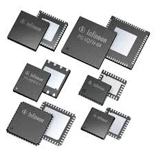
Quad Flat No-lead (QFN) components are a type of surface-mount device characterized by their compact size, excellent thermal performance, and lack of protruding leads. Instead of traditional leads, QFN packages have a planar copper lead frame that terminates at the bottom edge of the package, forming electrical connections when soldered to the PCB.
Advantages of QFN Components
QFN components offer several benefits that make them increasingly popular in modern electronics:
- Smaller footprint and lower profile
- Improved electrical performance due to shorter connection paths
- Enhanced thermal performance through exposed pad
- Reduced parasitic effects
- Cost-effective manufacturing
Challenges in QFN Assembly
Despite their advantages, QFN components present unique challenges in the assembly process:
- Difficulty in visual inspection of solder joints
- Potential for solder bridging between closely spaced pads
- Risk of insufficient solder on corner pads
- Voiding in the thermal pad area
- Sensitivity to moisture and handling
The Importance of Stencil Design in QFN Assembly
Role of Stencil Printing
Stencil printing is a critical step in the surface mount technology (SMT) process, responsible for depositing precise amounts of solder paste onto the PCB pads. For QFN components, accurate solder paste deposition is crucial for:
- Ensuring proper electrical connections
- Achieving optimal thermal performance
- Preventing solder defects such as bridging or insufficient solder
- Controlling voiding in the thermal pad area
Impact of Stencil Design on PCBA Performance
The stencil design directly influences the quality and reliability of the solder joints in QFN components. Proper stencil design can:
- Improve first-pass yield rates
- Enhance long-term reliability of the assembly
- Optimize thermal management
- Reduce rework and associated costs
- Ensure consistent electrical performance
Key Considerations in Stencil Design for QFN Components

Stencil Thickness
The thickness of the stencil plays a crucial role in determining the volume of solder paste deposited. For QFN components, consider the following:
- Typical stencil thickness ranges from 3 to 5 mils (0.076 to 0.127 mm)
- Thinner stencils (3-4 mils) are often used for fine-pitch QFNs
- Thicker stencils (4-5 mils) may be necessary for larger thermal pads
Aperture Design
Aperture design is critical for achieving the right solder paste volume and distribution. Key aspects include:
- Aperture size
- Aperture shape
- Area ratio
- Aspect ratio
Aperture Size
For QFN perimeter pads:
- Typically 1:1 ratio with pad size
- May be slightly reduced (80-90% of pad width) for fine-pitch QFNs
For thermal pads:
- Usually divided into smaller apertures
- Total aperture area typically 50-80% of the thermal pad area
Aperture Shape
- Rectangular apertures for perimeter pads
- Various shapes for thermal pad apertures (e.g., square, circular, or cross-shaped)
Area Ratio
Area ratio is the ratio of the aperture opening area to the aperture wall area. For reliable paste release:
- Aim for an area ratio ≥ 0.66 for square apertures
- Aim for an area ratio ≥ 0.60 for circular apertures
Aspect Ratio
Aspect ratio is the ratio of the aperture width to the stencil thickness. For optimal performance:
- Maintain an aspect ratio ≥ 1.5 for square apertures
- Maintain an aspect ratio ≥ 1.8 for circular apertures
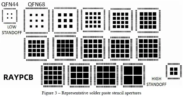
Thermal Pad Considerations
The thermal pad (exposed pad) of QFN components requires special attention in stencil design:
- Use multiple smaller apertures instead of a single large aperture
- Implement a “window pane” or gridded pattern
- Consider the use of “home plate” shaped apertures for corner coverage
- Adjust aperture sizes to control solder paste volume and voiding
Stencil Design Strategies for Different QFN Package Types
Fine-Pitch QFNs
For QFN packages with pitches below 0.5 mm:
- Use thinner stencils (3-4 mils)
- Reduce aperture width to 80-90% of pad width
- Consider stepped stencils for simultaneous fine-pitch and standard components
Large Thermal Pad QFNs
For QFNs with large thermal pads:
- Implement gridded aperture patterns
- Adjust aperture sizes to achieve 50-80% solder paste coverage
- Consider multi-level stencils for balanced paste deposition
Mixed-Technology Boards
When assembling boards with QFNs and other component types:
- Use step stencils to accommodate different paste volume requirements
- Consider multi-level stencils for complex mixed-technology designs
- Optimize aperture designs for each component type
Advanced Stencil Design Techniques
Stepped Stencils
Stepped stencils feature areas of different thicknesses, allowing for:
- Optimized paste volumes for different component types
- Improved solder paste release for fine-pitch QFNs
- Enhanced control over thermal pad solder volume
Multi-Level Stencils
Multi-level stencils offer even greater flexibility:
- Multiple thickness levels for complex mixed-technology boards
- Precise control over solder paste volume for various component types
- Improved first-pass yield rates in challenging designs
Nano-Coated Stencils
Nano-coated stencils feature a special surface treatment that:
- Enhances solder paste release, especially for fine-pitch applications
- Improves print definition and consistency
- Extends stencil life and reduces cleaning frequency
Stencil Material Selection
The choice of stencil material can significantly impact printing performance:
| Material | Characteristics | Best For |
| Stainless Steel | Durable, cost-effective | General purpose, high-volume production |
| Nickel | Smoother aperture walls, better release | Fine-pitch applications, challenging designs |
| Electroformed Nickel | Extremely smooth aperture walls, excellent release | Ultra-fine-pitch, critical applications |
| Laser-Cut Polyimide | Flexible, suitable for step stencils | Prototyping, low-volu |
Optimizing Stencil Design for QFN Components
Design Rules and Best Practices
- Maintain consistent aperture sizes for perimeter pads
- Use area and aspect ratio guidelines to ensure reliable paste release
- Implement gridded patterns for thermal pad apertures
- Consider component proximity and adjust apertures accordingly
- Use corner apertures or “home plate” designs for improved corner coverage
- Validate designs through simulation and testing
Simulation and Modeling
Utilize advanced simulation tools to:
- Predict solder paste behavior
- Optimize aperture designs
- Identify potential issues before production
Design for Manufacturing (DFM) Considerations
- Collaborate with your stencil manufacturer and assembly partner
- Consider the capabilities and limitations of available printing equipment
- Design for easy stencil cleaning and maintenance
- Implement fiducial marks for accurate stencil alignment
Troubleshooting Common QFN Stencil Printing Issues
| Issue | Possible Causes | Solutions |
| Insufficient Solder | Undersized apertures, poor paste release | Increase aperture size, adjust stencil thickness, consider nano-coating |
| Solder Bridging | Oversized apertures, excessive paste | Reduce aperture size, optimize stencil thickness, improve printer setup |
| Corner Lifting | Insufficient corner solder | Implement corner apertures, use “home plate” designs |
| Excessive Voiding | Improper thermal pad aperture design | Adjust gridded pattern, optimize aperture sizes |
| Inconsistent Printing | Stencil flexing, poor gasketing | Use tensioned stencils, improve |
Future Trends in QFN Stencil Design
As technology continues to evolve, several trends are emerging in QFN stencil design:
- Integration of artificial intelligence for optimized aperture designs
- Advanced materials for improved paste release and durability
- 3D-printed stencils for rapid prototyping and small-batch production
- Enhanced simulation tools for more accurate prediction of solder paste behavior
- Automated stencil design systems integrated with PCB design software
Conclusion
Stencil design plays a crucial role in the successful assembly of QFN components, directly impacting the performance, reliability, and yield of PCBAs. By understanding the key considerations, implementing advanced design techniques, and following best practices, engineers and designers can optimize their stencil designs for QFN components, ensuring high-quality assemblies that meet the demanding requirements of modern electronics.
As QFN packages continue to evolve and miniaturize, the importance of precise stencil design will only grow. Staying informed about the latest techniques, materials, and technologies in stencil design will be essential for maintaining a competitive edge in the rapidly advancing field of electronics manufacturing.
Frequently Asked Questions (FAQ)
1. What is the optimal stencil thickness for QFN components?
The optimal stencil thickness for QFN components typically ranges from 3 to 5 mils (0.076 to 0.127 mm). The specific thickness depends on several factors:
- QFN pitch: Fine-pitch QFNs (< 0.5 mm) often require thinner stencils (3-4 mils) for better control of solder paste volume.
- Thermal pad size: Larger thermal pads may benefit from thicker stencils (4-5 mils) to ensure sufficient solder paste volume.
- Mixed-technology boards: When assembling boards with various component types, a compromise thickness or step stencil may be necessary.
It’s important to balance the stencil thickness with aperture design to achieve optimal area and aspect ratios for reliable paste release.
2. How do I determine the appropriate aperture design for the thermal pad of a QFN?
Designing apertures for QFN thermal pads involves several considerations:
- Coverage area: Aim for 50-80% solder paste coverage of the total thermal pad area.
- Pattern: Use a gridded or “window pane” pattern rather than a single large aperture.
- Aperture shape: Consider square, circular, or cross-shaped apertures.
- Size distribution: Implement smaller apertures around the edges and larger ones in the center to promote outgassing.
- Corner coverage: Use “home plate” shaped apertures in the corners for better solder distribution.
Start with a standard pattern and adjust based on assembly results and thermal requirements. Simulation tools can help optimize the design before production.
3. What are the main differences in stencil design for fine-pitch QFNs compared to standard QFNs?
Stencil design for fine-pitch QFNs (typically < 0.5 mm pitch) requires special considerations:
- Thinner stencils: Usually 3-4 mils thick for better control of solder paste volume.
- Reduced aperture width: Often 80-90% of the pad width to prevent solder bridging.
- Stricter area and aspect ratios: More critical for ensuring reliable paste release.
- Nano-coatings: May be beneficial for improving paste release in challenging fine-pitch designs.
- Step stencils: Consider using step stencils when fine-pitch QFNs are combined with other component types on the same board.
These adjustments help manage the smaller solder paste volumes required for fine-pitch QFNs while maintaining reliable connections and preventing defects.
4. How can I minimize voiding in QFN thermal pads through stencil design?
Minimizing voiding in QFN thermal pads through stencil design involves several strategies:
- Optimize aperture pattern: Use a gridded pattern with spaces between apertures to allow for outgassing.
- Adjust aperture sizes: Implement smaller apertures around the edges and larger ones in the center to promote outward flow of volatiles.
- Control solder paste volume: Aim for 50-80% coverage of the thermal pad area to balance thermal performance and void reduction.
- Consider aperture shapes: Experiment with circular or cross-shaped apertures, which can promote better outgassing.
- Implement corner apertures: Use “home plate” shaped apertures in the corners to ensure good coverage while allowing gas escape paths.
- Fine-tune through testing: Adjust your design based on X-ray inspection results and thermal performance testing.
Remember that while stencil design is crucial, other factors like solder paste formulation, reflow profile, and PCB surface finish also play important roles in void reduction.
5. What are the advantages of using step stencils for QFN assembly?
Step stencils offer several advantages for QFN assembly, especially in mixed-technology boards:
- Optimized paste volumes: Different thicknesses can be used for various component types, ensuring appropriate solder paste volume for each.
- Improved fine-pitch printing: Thinner sections can be used for fine-pitch QFNs while maintaining thicker areas for standard components.
- Enhanced thermal pad control: Stepped areas can provide better control over solder paste volume for QFN thermal pads.
- Reduced need for compromise: Instead of choosing a single thickness that’s a compromise for all components, step stencils allow optimization for each area.
- Improved first-pass yield: By providing optimal solder paste volumes for different component types, step stencils can reduce assembly defects and improve overall yield.
- Cost-effective solution: While more expensive than standard stencils, step stencils can be more cost-effective than using multiple stencils or dealing with high rework rates.
When designing a step stencil, work closely with your stencil manufacturer to ensure the design is within their manufacturing capabilities and compatible with your printing equipment.