In the ever-evolving world of automotive electronics, the importance of reliable and durable printed circuit boards (PCBs) cannot be overstated. One crucial component in the PCB manufacturing process is the solder resist ink, also known as solder mask. This protective layer plays a vital role in ensuring the longevity and performance of automotive PCBs, which are subject to harsh environmental conditions and rigorous safety standards. In this comprehensive guide, we’ll explore the critical factors in selecting the best solder resist ink for automotive PCBs, delve into the various types available, and provide insights into the latest industry trends and innovations.

Understanding Solder Resist Ink and Its Importance in Automotive PCBs
What is Solder Resist Ink?
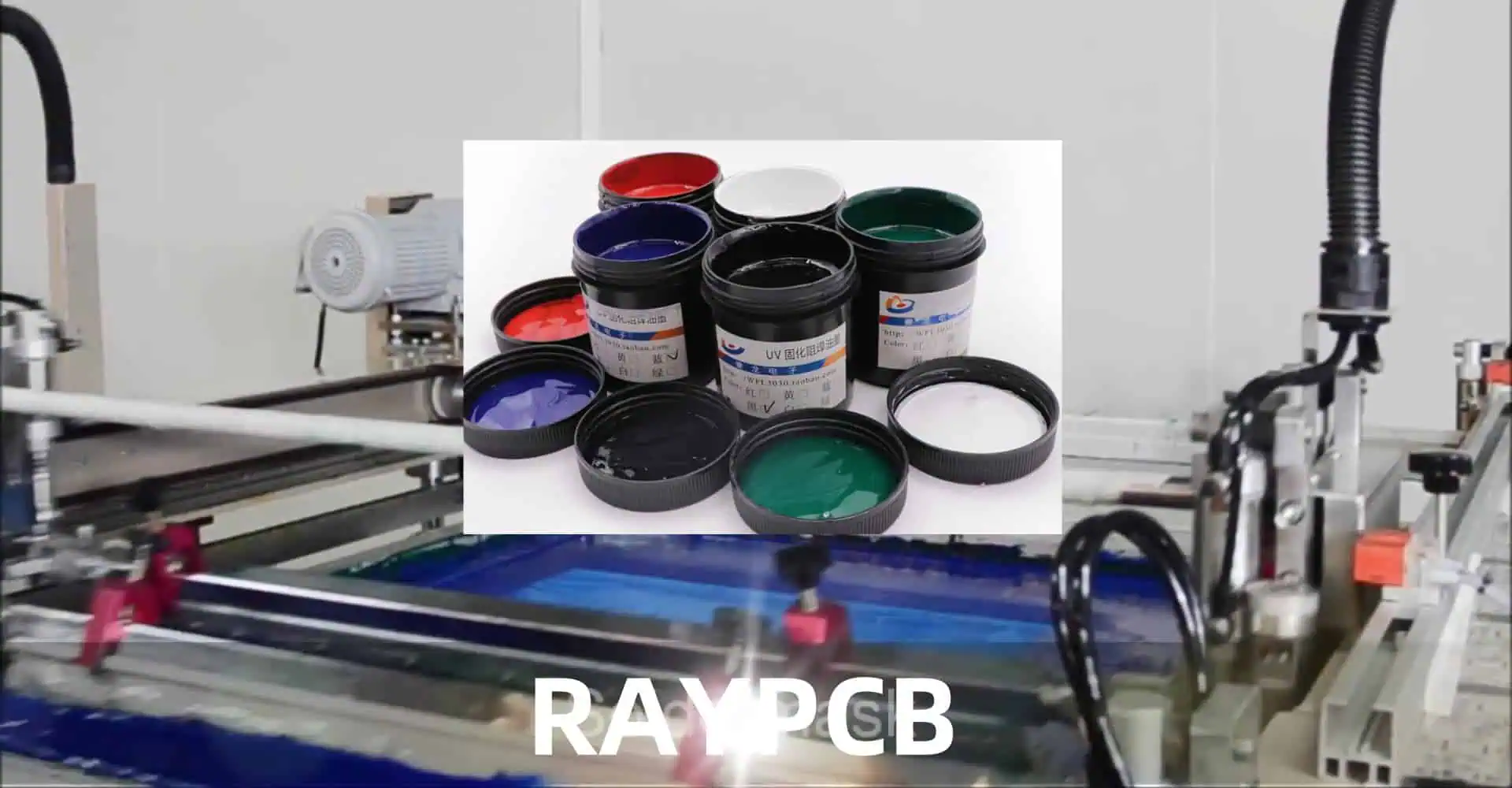
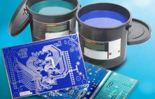
Solder resist ink is a polymer coating applied to the PCB surface to protect the copper traces from oxidation, moisture, dust, and short circuits. It also helps to control solder flow during the assembly process and provides insulation between conductive parts.
The Unique Demands of Automotive PCBs
Automotive PCBs face unique challenges compared to those used in consumer electronics:
- Extreme temperature variations
- Exposure to chemicals and fluids
- Constant vibration and shock
- Extended lifespan requirements
- Stringent safety and reliability standards
These factors make the choice of solder resist ink crucial for automotive PCB performance and longevity.
Key Properties to Consider When Choosing Solder Resist Ink
1. Temperature Resistance
Automotive PCBs must withstand extreme temperatures, from sub-zero conditions to the heat generated by engines and other components. The ideal solder resist ink should maintain its integrity across a wide temperature range.
2. Chemical Resistance
Exposure to automotive fluids, cleaning agents, and environmental pollutants requires solder resist inks with excellent chemical resistance to prevent degradation and maintain protection.
3. Adhesion Strength
Strong adhesion to the PCB substrate is essential to prevent peeling or flaking, which could lead to board failure.
4. Flexibility
The ability to withstand bending and flexing without cracking is crucial, especially in applications where the PCB may be subject to vibration or movement.
5. Dielectric Strength
High dielectric strength ensures proper insulation between conductive parts, preventing short circuits and improving overall PCB reliability.
6. Flame Retardancy
To meet automotive safety standards, solder resist inks must possess flame retardant properties to prevent fire hazards.
7. Curing Method and Time
The curing process affects production efficiency and the final properties of the solder resist layer. UV-curable inks are often preferred for their fast curing times and environmental friendliness.
8. Color Stability
Maintaining color stability over time, especially under UV exposure, is important for both aesthetic and functional reasons in automotive applications.
Types of Solder Resist Inks for Automotive PCBs
1. Liquid Photoimageable Solder Resist (LPSR)
LPSR is widely used in automotive PCB manufacturing due to its excellent resolution and ability to create fine patterns.
Advantages:
- High resolution for fine-pitch components
- Good chemical and thermal resistance
- Excellent adhesion to various substrates
Disadvantages:
- Requires multiple process steps (application, exposure, development)
- May have limitations in extreme temperature environments
2. Thermal Curable Solder Resist
This type of solder resist is cured using heat, which can provide excellent thermal stability.
Advantages:
- Superior heat resistance
- Good chemical resistance
- Simple application process
Disadvantages:
- Lower resolution compared to LPSR
- Longer curing times
3. UV Curable Solder Resist
UV curable solder resists offer fast curing times and are environmentally friendly.
Advantages:
- Rapid curing process
- Low VOC emissions
- Good flexibility
Disadvantages:
- May have limitations in high-temperature applications
- Requires special equipment for UV curing
4. Epoxy-based Solder Resist
Epoxy-based solder resists are known for their excellent chemical and thermal resistance.
Advantages:
- Outstanding chemical resistance
- Good adhesion to various substrates
- High temperature stability
Disadvantages:
- Can be brittle, potentially leading to cracking under extreme stress
- May yellow over time when exposed to UV light
Comparison of Solder Resist Ink Properties
| Property | LPSR | Thermal Curable | UV Curable | Epoxy-based |
| Temperature Resistance | Good | Excellent | Moderate | Excellent |
| Chemical Resistance | Very Good | Excellent | Good | Excellent |
| Adhesion Strength | Excellent | Very Good | Good | Excellent |
| Flexibility | Good | Moderate | Excellent | Poor to Moderate |
| Dielectric Strength | Very Good | Excellent | Good | Excellent |
| Flame Retardancy | Good | Excellent | Moderate | Excellent |
| Curing Time | Moderate | Long | Very Short | Long |
| Color Stability | Good | Very Good | Moderate | Moderate |
| Resolution | Excellent | Moderate | Good | Good |
Latest Innovations in Solder Resist Inks for Automotive PCBs

1. Nano-reinforced Solder Resists
Incorporating nanoparticles into solder resist formulations has led to significant improvements in mechanical strength, thermal conductivity, and chemical resistance.
2. High-Temperature Resistant Formulations
New formulations capable of withstanding temperatures up to 300°C have been developed to meet the demands of high-power automotive applications.
3. Self-healing Solder Resists
Emerging technologies in self-healing polymers show promise for creating solder resists that can repair minor damage autonomously, potentially extending PCB lifespan.
4. Low-temperature Curable Resists
These innovative formulations allow for curing at lower temperatures, reducing energy consumption and enabling the use of more temperature-sensitive components.
5. Conductive Solder Resists
While traditionally insulating, new conductive solder resist formulations are being developed for specific automotive applications, such as EMI shielding or heat dissipation.
Selecting the Best Solder Resist Ink for Your Automotive PCB Project
Factors to Consider:
- Application Requirements: Consider the specific environmental conditions and performance needs of your automotive PCB.
- Component Density: High-density boards with fine-pitch components may require LPSR for its superior resolution.
- Temperature Range: For high-temperature applications, thermal curable or epoxy-based resists may be more suitable.
- Production Volume and Speed: UV curable resists offer faster processing times for high-volume production.
- Regulatory Compliance: Ensure the chosen solder resist meets automotive industry standards such as IATF 16949 and AEC-Q100.
- Cost Considerations: Balance performance requirements with budget constraints, considering both material and processing costs.
- Compatibility: Ensure compatibility with other materials and processes used in your PCB manufacturing.
Decision-Making Process:
- Define your PCB’s specific requirements and operating conditions.
- Research and shortlist solder resist options that meet these requirements.
- Request samples and perform thorough testing under simulated conditions.
- Evaluate test results and consider long-term reliability projections.
- Consult with solder resist manufacturers and PCB fabrication experts.
- Make a final selection based on performance, cost, and production considerations.
Best Practices for Applying and Curing Solder Resist Ink
Surface Preparation
- Ensure the PCB surface is clean and free of contaminants.
- Use mechanical or chemical methods to create an optimal surface profile for adhesion.
- Perform a thorough cleaning process immediately before solder resist application.
Application Techniques
- Screen printing: Ideal for high-volume production and consistent thickness.
- Curtain coating: Provides excellent uniformity for large boards.
- Spray coating: Suitable for covering irregular surfaces and components.
Curing Process
- Follow manufacturer recommendations for curing parameters (time, temperature, UV intensity).
- Ensure even exposure or heat distribution across the entire board.
- Implement proper cooling procedures to prevent thermal stress.
Quality Control
- Perform visual inspections for defects such as pinholes, bubbles, or uneven coverage.
- Conduct electrical tests to verify insulation properties.
- Carry out environmental stress tests to simulate real-world conditions.
Future Trends in Automotive PCB Solder Resist Technology

- Integration of IoT and Smart Features: Solder resists with embedded sensors for real-time monitoring of PCB health and performance.
- Eco-friendly Formulations: Development of bio-based and fully recyclable solder resist materials to meet increasing sustainability demands.
- Additive Manufacturing Compatibility: Solder resists designed for 3D-printed electronics and flexible PCBs in automotive applications.
- Enhanced Thermal Management: Advanced formulations with improved heat dissipation properties to support high-power density designs.
- Multi-functional Coatings: Solder resists that combine protection with additional features such as EMI shielding or self-cleaning properties.
Conclusion
Selecting the best solder resist ink for automotive PCBs is a critical decision that impacts the reliability, performance, and longevity of electronic systems in vehicles. By understanding the unique demands of automotive environments, considering the key properties of different solder resist types, and staying informed about the latest innovations, manufacturers can make informed choices that meet the stringent requirements of the automotive industry.
As technology continues to advance, solder resist inks will play an increasingly important role in enabling the next generation of automotive electronics. From electric vehicles to autonomous driving systems, the demand for high-performance, reliable PCBs will only grow. By carefully selecting and properly applying the right solder resist ink, manufacturers can ensure their automotive PCBs are well-equipped to meet these challenges and drive innovation in the automotive industry.
Frequently Asked Questions (FAQ)
1. What is the difference between solder resist ink and conformal coating?
Solder resist ink is applied during the PCB manufacturing process and primarily protects against solder bridges and oxidation. Conformal coating is applied after component assembly and provides additional protection against moisture, chemicals, and environmental contaminants. While solder resist is essential for all PCBs, conformal coating is an optional extra layer of protection often used in harsh environments.
2. Can solder resist ink be removed or reworked?
Yes, solder resist ink can be removed or reworked, but it requires careful handling to avoid damaging the underlying copper traces. Common methods include mechanical abrasion, chemical stripping, or laser ablation. However, rework should be performed by skilled technicians and may affect the board’s long-term reliability.
3. How does the choice of solder resist ink affect PCB assembly processes?
The choice of solder resist ink can impact various assembly processes, including:
- Solder paste printing: The solder resist’s surface energy affects paste release and print quality.
- Component placement: Some resists may be more prone to scratching during placement.
- Reflow soldering: The resist’s temperature resistance is crucial for preventing degradation during reflow.
- Cleaning: Chemical resistance is important for compatibility with cleaning agents used post-assembly.
4. Are there specific color requirements for automotive PCB solder resists?
While green is the most common color for solder resists, automotive applications often use other colors for specific purposes:
- Black: For improved heat dissipation and aesthetic reasons in visible applications.
- White: To enhance reflectivity in LED applications or improve visual inspection.
- Red: Sometimes used as an indicator for high-voltage areas.
The color choice should also consider color stability under UV exposure and high temperatures.
5. How often should solder resist ink formulations be re-evaluated for automotive PCB projects?
It’s recommended to re-evaluate solder resist ink formulations regularly, typically every 2-3 years or when:
- New automotive standards or regulations are introduced.
- Significant advancements in solder resist technology emerge.
- Changes in PCB design or manufacturing processes occur.
- Performance issues are observed in current production.
Regular re-evaluation ensures that the chosen solder resist continues to meet the evolving demands of automotive electronics and takes advantage of the latest improvements in material technology.