Debugging a Non-Working PCB: A Comprehensive Guide

When you’ve invested hours designing a printed circuit board (PCB), ordered the components, carefully soldered everything in place, and powered it up for the first timeโ€”only to find it doesn’t workโ€”frustration is natural. However, debugging a non-working PCB is a methodical process that can be both educational and rewarding. With the right approach, tools, and patience, most PCB issues can be identified and resolved.

YouTube video

Initial Assessment and Safety

Before diving into debugging, ensure your workspace is safe and properly organized. Check that your power supply is set to the correct voltage and current limits. If your PCB is designed for 3.3V, accidentally applying 5V could damage sensitive components irreversibly. Always start with the lowest reasonable voltage and gradually increase while monitoring current consumption.

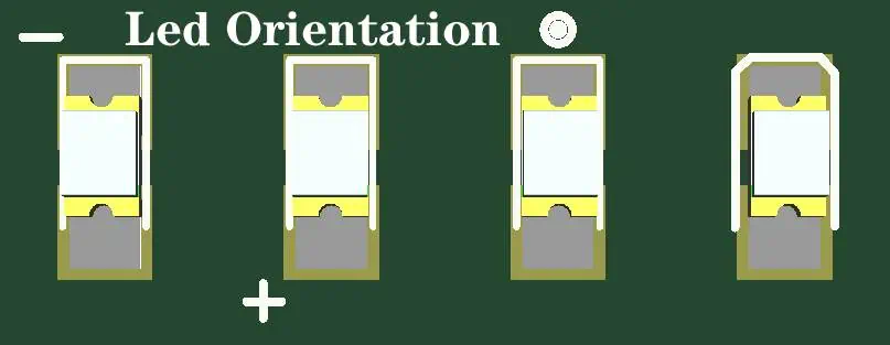
Begin with a visual inspection using good lighting and magnification. Look for obvious issues like solder bridges, cold solder joints, missing components, or components installed backwards. Pay special attention to polarized components such as diodes, electrolytic capacitors, and integrated circuits. A backwards diode or IC can prevent the entire circuit from functioning and may cause permanent damage.

Check your PCB against the schematic and bill of materials. It’s surprisingly easy to install the wrong value resistor or capacitor, especially when component markings are small or unclear. Verify that all components are present and correctly oriented. Use a multimeter to confirm resistor values if their color codes are difficult to read.

Power Supply Verification

PCB Programmer Debugger

Power issues are among the most common causes of non-working PCBs. Start by verifying that power is reaching your board correctly. Use a multimeter to check voltage levels at key points throughout your circuit. Begin at the power input and work your way through any voltage regulators to ensure each stage is functioning properly.

Measure both DC voltage levels and AC ripple. Excessive ripple can cause digital circuits to malfunction or analog circuits to produce noisy outputs. If you have access to an oscilloscope, examine the power supply waveforms under different load conditions. A switching regulator that works fine at light loads might become unstable or drop out under heavier loads.

Current consumption is equally important. If your circuit is drawing significantly more current than expected, you likely have a short circuit or a component failure. Conversely, if it’s drawing much less current than anticipated, critical components might not be powered or functioning. Use your power supply’s current limiting feature to protect your circuit while troubleshooting.

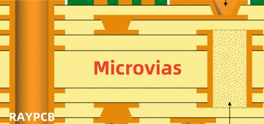
Ground connections are often overlooked but critical. Verify continuity between all ground points on your PCB. A broken ground connection can cause erratic behavior that’s difficult to diagnose. In multi-layer boards, via failures can create ground loops or isolated ground islands.

Systematic Signal Tracing

Once you’ve confirmed that power is distributed correctly, move on to signal tracing. Start from inputs and work toward outputs, or begin with known good signals and follow them through the circuit. This methodical approach helps isolate the problem to specific sections of your design.

For digital circuits, use a logic analyzer or oscilloscope to examine signal integrity. Check for proper voltage levels, timing relationships, and signal quality. Look for issues like ringing, overshoot, undershoot, or excessive rise/fall times. These problems often stem from improper termination, ground plane issues, or electromagnetic interference.

In analog circuits, signal tracing becomes more nuanced. Use an oscilloscope to examine waveforms at various stages of amplification or filtering. Compare measured results with your design calculations. Pay attention to frequency response, gain, offset voltages, and noise levels. A slight DC offset early in a signal chain can become a major problem after several stages of amplification.

Don’t forget about clock signals in digital systems. Clock integrity is crucial for proper operation. Verify that clock signals have appropriate amplitude, frequency, and duty cycle. Check for clock skew between different parts of your circuit, especially in high-speed designs.

Component-Level Testing

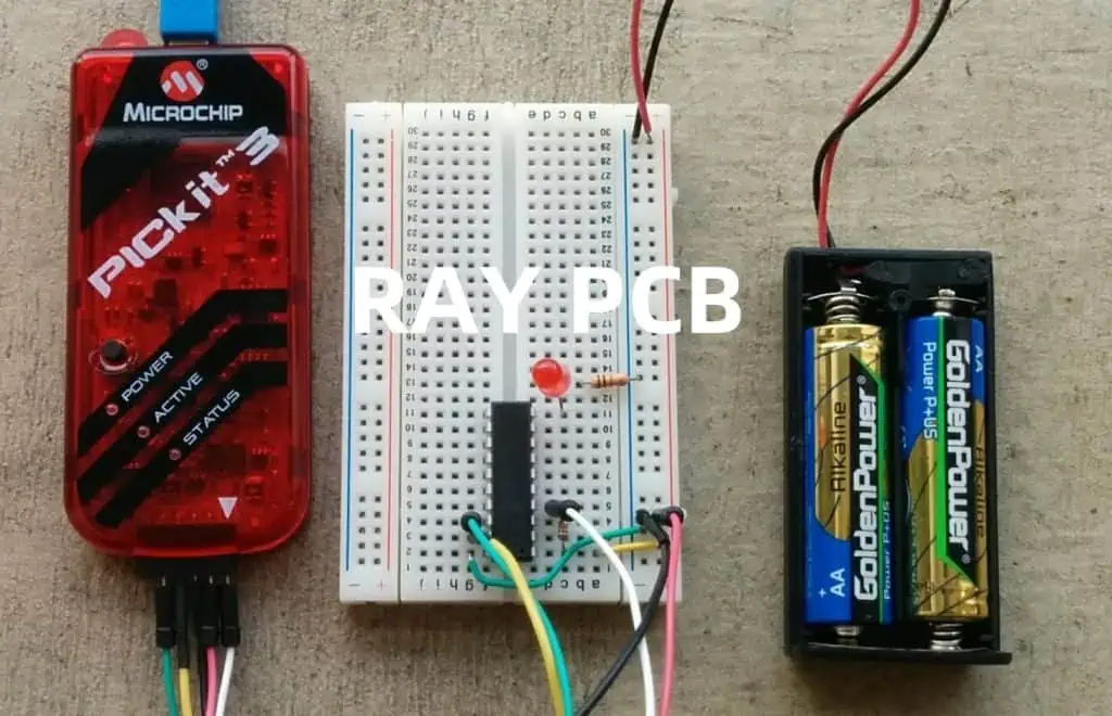
When system-level debugging doesn’t reveal the problem, it’s time to test individual components. Remove suspect components from the circuit when possible and test them independently. This is especially important for active components like transistors, operational amplifiers, and microcontrollers.

For semiconductors, check basic parameters like forward voltage drops on diodes, transistor beta values, and op-amp offset voltages. Compare these measurements with datasheet specifications. Components that test within specifications individually might still fail when operating in-circuit due to thermal effects or specific bias conditions.

Passive components can also fail in subtle ways. Capacitors might have correct capacitance but excessive equivalent series resistance (ESR) or leakage current. Inductors can have shorted turns that reduce their effective inductance. Even resistors can drift from their nominal values, especially if they’ve been stressed by overcurrent conditions.

Crystal oscillators deserve special attention in digital designs. These components are sensitive to loading conditions, temperature, and mechanical stress. If a crystal isn’t oscillating, check the load capacitors, bias resistors, and PCB layout around the oscillator circuit. Sometimes, simply touching the crystal with a probe is enough to start or stop oscillation, indicating a marginal design.

Advanced Debugging Techniques

For complex problems that resist conventional debugging approaches, advanced techniques may be necessary. Thermal imaging can reveal components that are running unexpectedly hot, indicating possible failures or design issues. Conversely, components that should be warm but remain cool might not be functioning at all.

In RF and high-frequency circuits, network analyzers can measure impedance, return loss, and insertion loss. These measurements help identify problems with transmission lines, matching networks, and filter circuits that might not be apparent with conventional instruments.

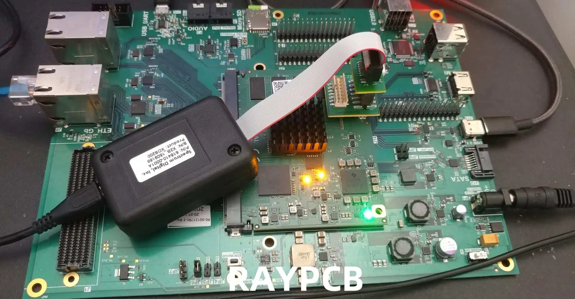
For microcontroller-based designs, in-circuit debugging tools like JTAG interfaces provide invaluable insight into program execution. You can set breakpoints, examine memory contents, and step through code execution to identify software-related issues. Sometimes what appears to be a hardware problem is actually a software bug.

Boundary scan testing, where available, allows you to test interconnections and basic functionality of digital ICs without removing them from the circuit. This technique is particularly useful for complex designs with fine-pitch components that are difficult to probe directly.

Environmental and Layout Considerations

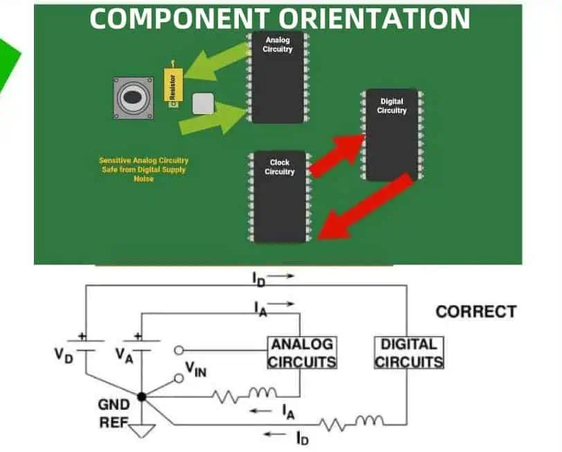
PCB layout issues can cause problems that are difficult to diagnose with conventional approaches. Poor ground plane design can create ground loops, causing noise and instability. Inadequate power plane design might cause voltage drops or noise coupling between different circuit sections.

Electromagnetic interference (EMI) can cause intermittent problems that are particularly frustrating to debug. Use an oscilloscope with good bandwidth to look for high-frequency noise on power and signal lines. Sometimes adding small bypass capacitors or ferrite beads can resolve these issues.

Thermal effects can cause components to behave differently than expected. Some failures only occur when the PCB reaches operating temperature, while others might disappear as components warm up. Use a heat gun or cooling spray to deliberately change component temperatures while monitoring circuit behavior.

Mechanical stress can also affect PCB performance. Flexing the board slightly while powered might reveal intermittent connection problems. Pay attention to areas where the PCB might be under mechanical stress, such as connector mounting points or areas near mounting holes.

Documentation and Prevention

Throughout the debugging process, maintain detailed documentation of your findings. Record which tests were performed, what measurements were taken, and what changes were made. This documentation becomes invaluable if similar problems occur in future designs or if you need to reproduce your debugging steps.

Consider implementing design for testability (DFT) features in future PCBs. Test points, LED indicators, and jumpers can significantly simplify debugging. Design in current measurement points and voltage monitoring capabilities where appropriate.

Review your design and manufacturing processes to prevent similar issues in the future. Was the problem caused by a design error, a manufacturing defect, or a component failure? Understanding root causes helps improve your design methodology and reduces the likelihood of similar problems in subsequent projects.

Conclusion

Debugging a non-working PCB requires patience, systematic thinking, and the right tools. Start with basic power and visual checks before moving to more sophisticated signal analysis. Remember that the most complex-seeming problems often have simple causesโ€”a backwards diode or solder bridge can render an entire design non-functional.

The debugging process, while sometimes frustrating, is an excellent learning opportunity. Each problem solved adds to your experience and makes future debugging efforts more efficient. With practice, you’ll develop an intuition for where problems are likely to occur and how to isolate them quickly.

Most importantly, don’t give up too quickly. Many PCB problems that initially seem insurmountable can be resolved with methodical debugging. The satisfaction of bringing a non-working design to life makes the effort worthwhile and contributes significantly to your growth as an electronics engineer.

Component Selection for PCBs โ€“ Common Mistakes

Selecting the right components for printed circuit board (PCB) design is a critical phase that can make or break a project’s success. Poor component choices often lead to increased costs, manufacturing delays, reliability issues, and even complete project failures. Understanding and avoiding common mistakes in component selection is essential for engineers at all levels, from hobbyists working on personal projects to professionals developing commercial products.

YouTube video

Package and Footprint Mismatches

One of the most fundamental yet frequently encountered mistakes is selecting components with incorrect packages or footprints. This error typically occurs when engineers focus solely on electrical specifications while overlooking physical dimensions and pin configurations. For instance, choosing a component available only in a Ball Grid Array (BGA) package when the design requires through-hole mounting for easy prototyping and repair can create significant manufacturing challenges.

The confusion often stems from component databases that list multiple package options for the same part number family. Engineers might select a component based on its electrical characteristics without verifying that the chosen package matches their PCB layout requirements. Surface-mount components are particularly prone to this issue, as packages like SOT-23, SOT-223, and TO-252 may appear similar but have vastly different thermal and electrical characteristics.

Additionally, land pattern compatibility poses another layer of complexity. Even when the package type is correct, variations in pad sizes, spacing, and thermal relief requirements can lead to assembly issues. Modern components often require specific land patterns defined by industry standards like IPC-7351, and deviating from these specifications can result in poor solder joint formation, thermal stress, or electrical performance degradation.

Inadequate Power and Thermal Management

Power-related component selection errors represent another major category of mistakes that can severely impact PCB performance and reliability. Engineers frequently underestimate power dissipation requirements, leading to component overheating, reduced lifespan, and potential failure under normal operating conditions.

Voltage regulators exemplify this challenge perfectly. Selecting a linear regulator when a switching regulator would be more appropriate can result in excessive heat generation and poor efficiency. Conversely, choosing an overly complex switching regulator for low-power applications can increase cost, board space, and electromagnetic interference unnecessarily. The thermal resistance from junction to ambient must be carefully calculated, considering not only the component’s internal thermal characteristics but also the PCB’s ability to dissipate heat through copper pours, thermal vias, and ambient airflow.

Power supply decoupling represents another area where mistakes frequently occur. Engineers often select capacitors based solely on capacitance values without considering equivalent series resistance (ESR), equivalent series inductance (ESL), and frequency response characteristics. High-frequency switching circuits require low-ESR capacitors placed strategically near power pins, while bulk energy storage might benefit from higher-capacity electrolytic capacitors despite their higher ESR.

Current handling capability extends beyond simple amperage ratings. Trace width, copper thickness, and temperature rise must be factored into component selection decisions. Connectors, switches, and fuses must be selected with adequate current margins, considering both steady-state and transient conditions. Inrush current, short-circuit protection, and derating factors based on ambient temperature all influence the appropriate component specifications.

Signal Integrity and High-Frequency Considerations

As operating frequencies continue to increase in modern electronic systems, signal integrity becomes increasingly critical in component selection. Engineers working with digital circuits often overlook the analog behavior of high-frequency signals, leading to poor component choices that degrade system performance.

Passive components like resistors, capacitors, and inductors exhibit parasitic effects that become significant at high frequencies. A standard ceramic capacitor might provide excellent performance at DC or low frequencies but exhibit significant inductance at MHz frequencies, making it unsuitable for high-speed decoupling applications. Similarly, carbon film resistors may introduce noise and exhibit frequency-dependent behavior that wire-wound or thin-film alternatives would handle better.

Connector selection becomes particularly challenging in high-frequency applications. Standard pin headers and terminal blocks that work perfectly for DC or low-frequency signals can introduce significant impedance discontinuities, crosstalk, and signal reflection in high-speed digital or RF circuits. Controlled impedance connectors, proper shielding, and matched transmission line characteristics become essential considerations.

Clock distribution presents another area where component selection mistakes are common. Crystal oscillators, clock buffers, and phase-locked loops must be selected not only for frequency accuracy but also for jitter performance, phase noise, and electromagnetic compatibility. A low-cost crystal oscillator might meet frequency requirements but introduce timing variations that cause data corruption in high-speed digital systems.

Environmental and Reliability Oversights

Environmental considerations in component selection are often underestimated, particularly in consumer electronics where products may be used in conditions far from ideal laboratory environments. Temperature ratings represent the most obvious environmental factor, but humidity, vibration, shock, and chemical exposure can equally impact component reliability.

Automotive, industrial, and outdoor applications require components with extended temperature ranges, often rated for -40ยฐC to +125ยฐC operation. Consumer-grade components typically rated for 0ยฐC to +70ยฐC may function initially but fail prematurely under extreme conditions. Military and aerospace applications have even more stringent requirements, necessitating components that meet specific qualification standards and traceability requirements.

Electrolytic capacitors are particularly sensitive to temperature and lifetime considerations. These components have finite lifespans that decrease exponentially with temperature and voltage stress. Selecting capacitors with inadequate voltage derating or temperature ratings can lead to premature failure, especially in applications with significant temperature cycling or extended operational requirements.

Mechanical stress factors are frequently overlooked, particularly in portable devices or equipment subject to vibration. Ceramic capacitors can crack under mechanical stress, while large components may require additional mechanical support to prevent solder joint failure. Flexible PCB applications require components specifically designed for bending stress, as standard rigid components may fail when subjected to repeated flexing.

Supply Chain and Lifecycle Management

Modern electronics development must consider component availability, lifecycle status, and supply chain resilience. Engineers often select components based purely on technical specifications without considering long-term availability, leading to costly redesigns when components become obsolete or unavailable.

Component lifecycle management requires understanding manufacturer roadmaps and industry trends. Selecting components that are already in end-of-life status or that use obsolete manufacturing processes can create significant challenges during production scaling or product maintenance phases. Preferred parts lists maintained by manufacturing partners can help guide component selection toward options with proven supply chain stability.

Single-source components represent a particular risk in today’s global supply chain environment. Selecting specialized components available from only one manufacturer can create supply bottlenecks and price volatility. Where possible, engineers should identify second-source alternatives or design flexibility that allows component substitution without significant PCB changes.

Lead times and minimum order quantities also impact component selection, particularly for low-volume or prototype applications. Components with long lead times or high minimum order quantities can significantly impact project schedules and budgets. Planning for component procurement early in the design process helps identify potential supply chain issues before they become critical.

Cost Optimization Mistakes

Cost considerations in component selection require balancing immediate component costs with long-term implications for manufacturing, testing, and maintenance. Engineers often focus on individual component prices without considering the total cost of ownership throughout the product lifecycle.

Over-specification represents a common cost mistake, where engineers select components with capabilities far exceeding application requirements. Using precision resistors in non-critical applications, specifying military-grade components for consumer products, or selecting high-speed operational amplifiers for DC applications can unnecessarily increase costs without providing corresponding benefits.

Conversely, under-specification in an attempt to reduce costs can lead to reliability issues, performance degradation, and expensive field failures. The cost of warranty repairs, customer support, and brand reputation damage often far exceeds the savings from using lower-grade components.

Volume pricing considerations become important for production quantities. Components that appear expensive in small quantities may offer significant cost advantages at production volumes due to volume pricing tiers. Understanding manufacturer pricing structures and working with distributors to optimize component costs can significantly impact overall product profitability.

Testing and Validation Considerations

Component selection must consider not only operational requirements but also testing and validation needs throughout the development process. Components that are difficult to test or require specialized equipment for validation can significantly increase development time and costs.

Built-in test features, diagnostic capabilities, and monitoring functions can simplify system validation and field troubleshooting. Selecting components with integrated test modes, status reporting, or fault detection can reduce external test circuitry requirements and improve system maintainability.

Prototype availability and evaluation support from component manufacturers can accelerate development timelines. Components with readily available evaluation boards, reference designs, and application support reduce development risk and time-to-market. Consideration of manufacturer support quality, documentation completeness, and technical expertise availability should factor into component selection decisions.

Conclusion

Successful PCB component selection requires a holistic approach that considers electrical performance, physical constraints, environmental requirements, supply chain factors, and cost implications. Avoiding common mistakes requires systematic evaluation of each component choice against multiple criteria, not just primary electrical specifications.

The complexity of modern electronic systems demands that engineers develop comprehensive component selection processes that account for the interconnected nature of these various factors. Regular review of component choices throughout the design process, combined with lessons learned from previous projects, helps build the experience and judgment necessary for making sound component selection decisions.

Ultimately, successful component selection contributes significantly to overall project success, affecting everything from initial development timelines to long-term product reliability and profitability. Investing time and effort in proper component selection early in the design process pays dividends throughout the entire product lifecycle.

BGA ROUTING AND IMPEDANCE CONTROL IN HDI PCBs

In the rapidly evolving world of electronics, High-Density Interconnect (HDI) Printed Circuit Boards (PCBs) have become crucial for meeting the demands of miniaturization and increased functionality. Among the challenges faced by PCB designers, Ball Grid Array (BGA) routing and impedance control stand out as critical aspects that significantly impact the performance and reliability of electronic devices. This article delves into the intricacies of BGA routing and impedance control in HDI PCBs, exploring best practices, challenges, and emerging technologies in this field.

YouTube video

Understanding BGA Technology

What is BGA?

Ball Grid Array (BGA) is a surface-mount packaging technology for integrated circuits. It is designed to address the increasing demand for higher pin counts and better electrical and thermal performance in a compact form factor.

Advantages of BGA

  1. Higher pin count in a smaller area
  2. Better thermal and electrical performance
  3. Reduced lead inductance
  4. Improved reliability due to self-alignment during reflow

Types of BGA Packages

BGA TypeDescriptionTypical Application
Plastic BGA (PBGA)Uses plastic substrateConsumer electronics
Ceramic BGA (CBGA)Uses ceramic substrateHigh-reliability applications
Tape BGA (TBGA)Uses polyimide tape substrateLightweight applications
Micro BGA (BGA)Smaller pitch, typically < 0.8mmMobile devices
Flip Chip BGA (FCBGA)Die is flipped and connected directly to substrateHigh-performance computing

HDI PCB Technology

Definition of HDI

High-Density Interconnect (HDI) PCBs are characterized by higher wiring density per unit area. They typically feature finer lines and spaces, smaller vias and capture pads, and higher connection pad density than traditional PCBs.

Key Features of HDI PCBs

  1. Microvias (laser-drilled vias with diameter < 150ยตm)
  2. Fine line width and spacing (typically < 100ยตm)
  3. High layer count (often > 10 layers)
  4. Buried and blind vias
  5. Sequential lamination process

Benefits of HDI in BGA Routing

  1. Improved signal integrity
  2. Reduced board size and weight
  3. Enhanced electrical performance
  4. Better thermal management
  5. Increased design flexibility

BGA Routing Strategies in HDI PCBs

Fanout Techniques

1. Dog Bone Fanout

  • Description: Uses short traces (“dog bones”) to connect BGA pads to vias
  • Pros: Simple, cost-effective
  • Cons: Limited routing density, longer signal paths

2. Via-in-Pad

  • Description: Vias placed directly in BGA pads
  • Pros: Highest density, shortest signal paths
  • Cons: More complex manufacturing, potential reliability issues

3. Via-near-Pad

  • Description: Vias placed adjacent to BGA pads
  • Pros: Balance between density and manufacturability
  • Cons: Slightly longer signal paths than via-in-pad

Layer Stack-up Considerations

  1. Signal layer allocation
  2. Power and ground plane placement
  3. Microvia structure (stacked, staggered, or skip vias)

Routing Guidelines

  1. Maintain consistent trace widths
  2. Use 45-degree angles for direction changes
  3. Implement differential pair routing for high-speed signals
  4. Avoid routing under BGA to minimize crosstalk
  5. Consider signal grouping and length matching

Impedance Control in HDI PCBs

Importance of Impedance Control

Impedance control is crucial for maintaining signal integrity, especially in high-speed designs. It helps minimize signal reflections, reduce electromagnetic interference (EMI), and ensure proper signal transmission.

Factors Affecting Impedance

  1. Trace width
  2. Trace thickness
  3. Dielectric constant of PCB material
  4. Distance to reference planes
  5. Presence of nearby conductors

Common Impedance Values

ApplicationTypical Impedance
Single-ended50ฮฉ or 75ฮฉ
Differential100ฮฉ or 120ฮฉ
USB90ฮฉ differential
HDMI100ฮฉ differential
PCIe100ฮฉ differential

Impedance Calculation

While exact impedance calculations can be complex, a simplified formula for microstrip impedance is:

Zโ‚€ = 87 / โˆš(ฮตแตฃ + 1.41) * ln(5.98h / (0.8w + t))

Where:

  • Zโ‚€ is the characteristic impedance
  • ฮตแตฃ is the dielectric constant of the PCB material
  • h is the height of the trace above the ground plane
  • w is the width of the trace
  • t is the thickness of the trace

Impedance Control Techniques

1. Controlled Dielectric Thickness

HDI PCB Board Laminate Structure-PCB Manufacturer-4
  • Maintain consistent dielectric thickness between signal layers and adjacent planes
  • Use high-quality, low-tolerance PCB materials

2. Trace Width Control

  • Adjust trace widths to achieve desired impedance
  • Use impedance calculators or field solvers for accurate calculations

3. Copper Weight Management

  • Consider the impact of copper thickness on impedance
  • Use consistent copper weights across the board

4. Reference Plane Design

  • Ensure solid, uninterrupted reference planes
  • Implement proper return path design

5. Differential Pair Routing

  • Maintain consistent spacing between differential pairs
  • Use serpentine routing for length matching

Challenges in BGA Routing and Impedance Control

1. High-Density Routing

  • Limited space for routing between BGA pads
  • Need for advanced PCB fabrication techniques

2. Signal Integrity

  • Managing crosstalk and EMI in dense layouts
  • Maintaining consistent impedance across the board

3. Thermal Management

  • Dealing with heat dissipation in high-pin-count BGAs
  • Balancing thermal and electrical requirements

4. Manufacturing Complexity

  • Increased cost due to more complex fabrication processes
  • Higher potential for manufacturing defects

5. Testing and Inspection

  • Limited access to BGA solder joints for inspection
  • Need for advanced testing techniques (e.g., X-ray inspection)

Advanced Techniques and Future Trends

1. 3D Routing

2. AI-Assisted Routing

  • Using machine learning algorithms for optimal trace routing
  • Automated impedance control and signal integrity analysis

3. Advanced Materials

  • Development of low-loss, high-speed PCB materials
  • Implementation of novel dielectrics for improved performance

4. Optical Interconnects

  • Integration of optical layers in HDI PCBs
  • Hybrid electro-optical routing solutions

5. Additive Manufacturing

  • 3D-printed PCBs with integrated BGA routing
  • Custom impedance control through additive processes

Best Practices for BGA Routing and Impedance Control

  1. Use appropriate design tools and simulators
  2. Implement a well-planned layer stack-up
  3. Follow manufacturer’s guidelines for BGA fanout
  4. Perform thorough signal integrity analysis
  5. Use controlled impedance techniques consistently
  6. Implement proper power distribution network (PDN) design
  7. Consider thermal management early in the design process
  8. Collaborate closely with PCB fabricators and assemblers
  9. Implement robust design for manufacturability (DFM) practices
  10. Conduct thorough testing and verification before production

Conclusion

BGA routing and impedance control in HDI PCBs represent critical challenges in modern electronic design. As devices continue to shrink in size while increasing in complexity and performance, mastering these aspects becomes essential for creating reliable, high-performance electronics.

The successful implementation of BGA routing and impedance control requires a deep understanding of PCB design principles, material properties, and manufacturing processes. Designers must balance the demands of high-density routing with the need for signal integrity, thermal management, and manufacturability.

As we look to the future, emerging technologies such as 3D routing, AI-assisted design, and advanced materials promise to push the boundaries of what’s possible in HDI PCB design. However, these advancements will also bring new challenges that designers must be prepared to address.

Ultimately, the key to success in BGA routing and impedance control lies in a holistic approach to PCB design, combining technical expertise with creativity and a willingness to embrace new technologies and methodologies. By following best practices and staying abreast of industry developments, designers can create HDI PCBs that meet the ever-increasing demands of modern electronics.

FAQ

Q1: What are the main advantages of using BGAs in HDI PCB designs?

A1: The main advantages of using BGAs in HDI PCB designs include:

  1. Higher pin count in a smaller area, allowing for more compact designs
  2. Improved electrical performance due to shorter interconnects and reduced parasitic effects
  3. Better thermal performance, as the entire bottom surface of the package can be used for heat dissipation
  4. Reduced lead inductance, which is crucial for high-speed applications
  5. Self-alignment during the reflow process, which can improve manufacturing yield
  6. More robust mechanical connection compared to leaded packages
  7. Ability to accommodate complex ICs with high I/O requirements

Q2: How does impedance control impact signal integrity in HDI PCBs?

A2: Impedance control significantly impacts signal integrity in HDI PCBs in several ways:

  1. Minimizes signal reflections: Consistent impedance along the signal path reduces reflections that can cause signal distortion.
  2. Reduces electromagnetic interference (EMI): Proper impedance control helps contain electromagnetic fields, reducing unwanted radiation and coupling.
  3. Improves signal quality: Controlled impedance environments maintain signal shape and timing, crucial for high-speed data transmission.
  4. Enhances power integrity: Well-controlled impedance in power distribution networks helps maintain stable power delivery to components.
  5. Enables faster edge rates: Consistent impedance allows for faster signal transition times without degradation.
  6. Facilitates matching: Controlled impedance makes it easier to match source, transmission line, and load impedances, maximizing power transfer.
  7. Supports higher bandwidth: By maintaining signal quality, impedance control enables higher data rates and bandwidth in digital systems.

Q3: What are the key challenges in routing high pin-count BGAs in HDI PCBs?

A3: Routing high pin-count BGAs in HDI PCBs presents several key challenges:

  1. Limited space: The high density of BGA pins leaves little room for routing between pads.
  2. Layer count management: Balancing the need for multiple routing layers with manufacturing constraints and cost considerations.
  3. Via management: Efficiently using and placing microvias to access inner layers without blocking too many routing channels.
  4. Signal integrity: Maintaining proper signal quality, especially for high-speed signals, in a dense routing environment.
  5. Power delivery: Ensuring adequate power and ground connections to all parts of the BGA.
  6. Thermal management: Dealing with heat dissipation in high-pin-count, densely routed areas.
  7. Manufacturability: Ensuring the design can be reliably manufactured and assembled despite its complexity.
  8. Impedance control: Maintaining consistent impedance in a constrained routing space.
  9. Crosstalk minimization: Managing electromagnetic coupling between closely spaced traces.
  10. Testability: Providing adequate test points and implementing design-for-test strategies in a limited-access environment.

Q4: How does the choice of PCB material affect impedance control in HDI designs?

A4: The choice of PCB material significantly affects impedance control in HDI designs in several ways:

  1. Dielectric constant: Materials with lower and more stable dielectric constants allow for more precise impedance control.
  2. Loss tangent: Lower loss tangent materials reduce signal attenuation, especially at high frequencies.
  3. Thickness control: Materials with tighter thickness tolerances enable more accurate impedance calculations and control.
  4. Thermal stability: Materials with lower coefficients of thermal expansion (CTE) maintain more consistent impedance across temperature ranges.
  5. Moisture absorption: Materials with lower moisture absorption rates maintain more stable electrical properties over time.
  6. Frequency dependence: Some materials maintain more consistent properties across a wide frequency range, crucial for broadband applications.
  7. Copper adhesion: Better copper adhesion allows for finer lines and spaces, enabling more precise impedance control.
  8. Homogeneity: More homogeneous materials provide more consistent electrical properties across the board.
  9. Cost: High-performance materials often come at a higher cost, requiring a balance between performance and budget.

Q5: What emerging technologies are likely to impact BGA routing and impedance control in the future?

A5: Several emerging technologies are poised to impact BGA routing and impedance control:

  1. 3D printing of PCBs: Enabling complex 3D routing strategies and custom impedance structures.
  2. AI-assisted routing: Using machine learning algorithms to optimize BGA breakout and routing patterns.
  3. Advanced PCB materials: Development of novel substrate materials with improved electrical and thermal properties.
  4. Embedded components: Integrating passive and active components within PCB layers to free up surface routing space.
  5. Optical interconnects: Incorporating optical layers in HDI PCBs for high-speed, low-loss signal transmission.
  6. Additive manufacturing techniques: Allowing for more precise control of trace geometries and material deposition.
  7. Advanced simulation tools: More accurate and efficient electromagnetic and thermal simulation capabilities.
  8. Photonic PCBs: Integration of optical waveguides with traditional PCB technology for ultra-high-speed applications.
  9. Flexible and stretchable electronics: New form factors requiring novel approaches to BGA mounting and impedance control.
  10. Quantum computing integration: Adapting PCB design for quantum computing requirements, including cryogenic operations and specialized signal routing.

CSP AND FINE-PITCH PCB ASSEMBLY

eMMC BGA

In the ever-evolving world of electronics, the demand for smaller, faster, and more powerful devices continues to drive innovation in printed circuit board (PCB) assembly techniques. Two key technologies at the forefront of this miniaturization trend are Chip Scale Packaging (CSP) and fine-pitch assembly. This article explores these cutting-edge approaches, their benefits, challenges, and their impact on the electronics manufacturing industry.

YouTube video

Understanding Chip Scale Packaging (CSP)

Definition and Characteristics

Chip Scale Packaging (CSP) is an advanced integrated circuit (IC) packaging technology where the package is no more than 1.2 times the size of the die. CSPs are designed to minimize the physical size of electronic components while maintaining or improving their performance.

Key characteristics of CSPs include:

  1. Small form factor
  2. Direct surface mountable
  3. Reduced parasitics
  4. Improved thermal performance
  5. Enhanced electrical characteristics

Types of CSP

1. Flip Chip CSP

Flip Chip
Flip Chip

Flip Chip CSP involves mounting the chip face-down on the substrate, with connections made through small solder bumps.

2. Wire Bonded CSP

In this type, the chip is connected to the package substrate using wire bonds before being encapsulated.

3. Wafer Level CSP (WLCSP)

WLCSP is created directly on the wafer before singulation, resulting in a package the same size as the die.

4. Stacked CSP

Multiple chips are stacked vertically within a single package, allowing for even greater miniaturization.

Advantages of CSP

  1. Reduced footprint and weight
  2. Improved electrical performance due to shorter interconnects
  3. Better thermal management
  4. Higher I/O density
  5. Cost-effective for high-volume production

Challenges in CSP Implementation

  1. Requires advanced assembly equipment
  2. More sensitive to thermal stress
  3. Increased complexity in PCB design
  4. Potential reliability issues due to smaller solder joints

Fine-Pitch PCB Assembly

Definition and Importance

Fine-pitch assembly refers to the process of placing and soldering components with very close lead spacing on a PCB. As electronic devices become smaller and more complex, the need for fine-pitch assembly has become crucial.

Fine-Pitch Categories

CategoryLead Pitch
Standard> 0.65 mm
Fine0.4 mm – 0.65 mm
Ultra-Fine0.3 mm – 0.4 mm
Super-Fine< 0.3 mm

Key Technologies in Fine-Pitch Assembly

1. Advanced Pick-and-Place Machines

Modern pick-and-place machines offer high accuracy and speed, capable of placing components with pitches as small as 0.3 mm or less.

2. High-Precision Stencil Printing

Stencil printing technology has evolved to accommodate fine-pitch requirements, with improvements in stencil materials, designs, and printing processes.

3. Reflow Soldering Optimization

Reflow profiles must be carefully optimized to ensure proper solder joint formation without causing component damage or solder bridging.

4. Automated Optical Inspection (AOI)

AOI systems play a crucial role in detecting defects in fine-pitch assemblies, offering high-resolution imaging and advanced algorithms for defect detection.

Challenges in Fine-Pitch Assembly

  1. Increased risk of solder bridging
  2. Difficulty in rework and repair
  3. Higher sensitivity to PCB warpage and coplanarity issues
  4. Stringent requirements for component placement accuracy
  5. Need for advanced inspection techniques

PCB Design Considerations for CSP and Fine-Pitch Assembly

Xilinx Versal FPGA
Xilinx Versal FPGA

Layout and Routing

  1. Careful planning of component placement
  2. Use of microvias and HDI techniques
  3. Consideration of signal integrity and power distribution
  4. Implementation of proper thermal management strategies

Solder Pad Design

  1. Optimization of pad size and shape
  2. Use of solder mask defined (SMD) vs. non-solder mask defined (NSMD) pads
  3. Implementation of proper pad finish (e.g., ENIG, HASL)

Design for Manufacturability (DFM)

  1. Adherence to minimum spacing rules
  2. Consideration of pick-and-place machine capabilities
  3. Design for testability and inspection

Material Selection

  1. Use of appropriate PCB substrate materials
  2. Selection of solder paste with suitable particle size and flux characteristics
  3. Consideration of underfill materials for certain CSP applications

Manufacturing Process for CSP and Fine-Pitch Assembly

1. PCB Fabrication

  • High-precision drilling and etching
  • Implementation of advanced PCB technologies (e.g., HDI, microvias)

2. Solder Paste Printing

  • Use of ultra-fine pitch stencils
  • Optimization of printing parameters (speed, pressure, separation speed)
  • Implementation of automated solder paste inspection (SPI)

3. Component Placement

  • Use of advanced pick-and-place machines with high accuracy
  • Implementation of fiducial marks for improved placement precision
  • Consideration of component-specific placement requirements

4. Reflow Soldering

  • Development of optimized reflow profiles
  • Use of nitrogen atmosphere for improved soldering results
  • Implementation of proper cooling strategies

5. Inspection and Quality Control

  • Automated optical inspection (AOI) for solder joint and placement verification
  • X-ray inspection for hidden solder joints (e.g., BGA, CSP)
  • Implementation of in-circuit testing (ICT) and functional testing

6. Rework and Repair (if necessary)

  • Use of specialized rework stations for CSP and fine-pitch components
  • Implementation of proper handling and ESD protection procedures

Advanced Techniques in CSP and Fine-Pitch Assembly

1. 3D Package Integration

  • Stacking of multiple CSPs
  • Integration of different component types within a single package

2. Embedded Components

  • Incorporation of passive and active components within PCB layers
  • Reduction of overall PCB size and improvement of electrical performance

3. Laser-Assisted Bonding

  • Use of laser technology for precise solder reflow
  • Enablement of ultra-fine pitch assembly

4. Plasma Cleaning

  • Implementation of plasma cleaning processes to improve solder joint reliability
  • Enhancement of surface wettability for improved solder paste adhesion

5. Conformal Coating

  • Application of protective coatings to improve reliability in harsh environments
  • Use of advanced coating materials and application techniques

Industry Trends and Future Outlook

xilinx-spartan-6-fpga-tutorial

Miniaturization Trends

The push for smaller, more powerful devices continues to drive the development of even smaller CSPs and finer pitch assemblies.

YearMinimum CSP SizeMinimum Lead Pitch
20200.4 mm x 0.4 mm0.3 mm
20220.3 mm x 0.3 mm0.25 mm
2024 (projected)0.2 mm x 0.2 mm0.2 mm
2026 (projected)0.15 mm x 0.15 mm0.15 mm

Integration with Advanced Technologies

  1. 5G and high-frequency applications
  2. Internet of Things (IoT) devices
  3. Artificial Intelligence (AI) and machine learning hardware
  4. Automotive electronics
  5. Wearable technology

Sustainability and Environmental Considerations

  1. Development of lead-free and halogen-free CSP solutions
  2. Implementation of more energy-efficient assembly processes
  3. Focus on recyclability and end-of-life considerations in package design

Automation and Industry 4.0

  1. Increased use of AI and machine learning in assembly processes
  2. Implementation of digital twin technology for process optimization
  3. Development of fully automated, lights-out manufacturing facilities

Conclusion

CSP and fine-pitch PCB assembly technologies have revolutionized the electronics industry, enabling the creation of smaller, more powerful devices that were once thought impossible. As we continue to push the boundaries of miniaturization, these technologies will play an increasingly critical role in shaping the future of electronics.

The challenges associated with CSP and fine-pitch assembly are significant, requiring ongoing innovation in materials, processes, and equipment. However, the benefits in terms of device performance, size reduction, and functionality make these challenges worth overcoming.

As the industry moves forward, we can expect to see even more advanced packaging solutions, finer pitches, and more integrated assemblies. The convergence of CSP and fine-pitch technologies with other emerging trends such as 3D integration, embedded components, and advanced materials will likely lead to new breakthroughs in electronic device design and manufacturing.

The future of CSP and fine-pitch PCB assembly is bright, promising continued innovation and exciting new possibilities in the world of electronics. As these technologies evolve, they will enable the next generation of electronic devices that will shape our increasingly connected and technology-driven world.

FAQ

Q1: What is the main difference between CSP and traditional IC packaging?

A1: The main difference lies in the size and efficiency of the package. Chip Scale Packaging (CSP) is designed to be very close to the size of the actual silicon die, typically no more than 1.2 times the size of the die. Traditional IC packages, on the other hand, are often significantly larger than the die they contain. CSPs offer several advantages, including:

  1. Smaller footprint on the PCB
  2. Improved electrical performance due to shorter interconnects
  3. Better thermal characteristics
  4. Higher I/O density
  5. Often more cost-effective for high-volume production

Q2: What are the key challenges in implementing fine-pitch PCB assembly?

A2: Implementing fine-pitch PCB assembly comes with several challenges:

  1. Increased risk of solder bridging due to closer component leads
  2. Higher demands on placement accuracy for pick-and-place machines
  3. Need for more precise stencil printing to control solder paste volume
  4. Difficulty in inspection and quality control due to smaller features
  5. Increased sensitivity to PCB warpage and coplanarity issues
  6. Challenges in rework and repair of defective joints
  7. Requirements for more advanced PCB design techniques, such as the use of microvias

Q3: How does the use of CSPs and fine-pitch assembly impact PCB design?

A3: The use of CSPs and fine-pitch assembly significantly impacts PCB design in several ways:

  1. Requires more careful component placement and routing to manage the higher density
  2. Often necessitates the use of advanced PCB technologies like High-Density Interconnect (HDI) and microvias
  3. Demands greater attention to signal integrity due to closer proximity of components
  4. Requires more sophisticated power distribution network design
  5. Necessitates careful thermal management strategies
  6. Calls for stricter adherence to design for manufacturability (DFM) guidelines
  7. Often requires the use of more advanced PCB materials to meet performance requirements

Q4: What are some emerging technologies that complement CSP and fine-pitch assembly?

A4: Several emerging technologies are complementing and enhancing CSP and fine-pitch assembly:

  1. 3D package integration, allowing for vertical stacking of multiple chips
  2. Embedded component technology, integrating passive and active components within PCB layers
  3. Advanced materials, such as low-loss dielectrics for high-frequency applications
  4. Laser-assisted bonding for ultra-fine pitch assembly
  5. Plasma cleaning processes to improve solder joint reliability
  6. Advanced inspection technologies, including high-resolution X-ray and 3D AOI systems
  7. AI and machine learning for process optimization and defect prediction

Q5: How is the industry addressing the environmental concerns related to CSP and fine-pitch assembly?

A5: The industry is addressing environmental concerns through several initiatives:

  1. Development of lead-free and halogen-free CSP solutions to comply with regulations like RoHS
  2. Implementation of more energy-efficient assembly processes to reduce carbon footprint
  3. Design for recyclability, considering end-of-life disassembly and material recovery
  4. Use of more environmentally friendly flux and cleaning agents in the assembly process
  5. Optimization of manufacturing processes to reduce waste and improve yield
  6. Development of more durable designs to extend product lifespan
  7. Implementation of circular economy principles in the electronics supply chain

Micro-Hole Technology for HDI PCBs

What is Micro-Hole Technology?

Micro-hole technology represents a revolutionary advancement in printed circuit board (PCB) manufacturing, specifically designed to meet the demanding requirements of High Density Interconnect (HDI) boards. This sophisticated drilling technique creates extremely small holes, typically ranging from 50 to 150 micrometers in diameter, which are significantly smaller than traditional mechanical drill holes that usually measure 200 micrometers or larger.

The technology enables manufacturers to create intricate interconnections between different layers of multilayer PCBs, allowing for unprecedented component density and miniaturization. These microscopic holes serve as pathways for electrical signals, connecting traces on different layers while occupying minimal board real estate.

YouTube video

Types of Micro-Holes in HDI PCBs

Microvias

Microvias are the most common type of micro-holes found in HDI PCBs. These small-diameter holes connect adjacent layers and are typically created using laser drilling technology. Microvias can be categorized into several types:

Blind vias connect an outer layer to one or more inner layers without penetrating the entire board thickness. These vias are essential for maintaining signal integrity in high-speed applications while preserving valuable routing space on internal layers.

Buried vias exist entirely within the internal layers of the PCB, connecting two or more inner layers without reaching either outer surface. This design approach maximizes routing density and allows for more complex interconnection schemes.

Stacked vias involve multiple microvias placed directly on top of each other, creating connections through multiple layers. This configuration requires precise alignment and advanced manufacturing capabilities but offers exceptional routing flexibility.

Through Holes vs. Micro-Holes

Traditional through holes penetrate the entire PCB thickness and are primarily used for component mounting and layer-to-layer connections in conventional designs. In contrast, micro-holes in HDI technology offer several advantages:

The smaller diameter reduces the capture pad size, freeing up valuable routing space around components. This space efficiency is crucial in modern electronic devices where every square millimeter counts.

Micro-holes also provide superior electrical performance due to their reduced parasitic capacitance and inductance, making them ideal for high-frequency applications where signal integrity is paramount.

Manufacturing Processes for Micro-Holes

Laser Drilling Technology

Laser drilling has become the predominant method for creating micro-holes in HDI PCBs due to its precision and versatility. The process uses focused laser beams to ablate material, creating clean, precise holes with minimal thermal damage to surrounding areas.

CO2 lasers are commonly used for drilling through organic materials like prepreg and core materials. These lasers operate at a wavelength of 10.6 micrometers and are particularly effective at removing resin-based materials.

UV lasers excel at drilling through copper layers and provide exceptional precision for the smallest diameter holes. Operating at wavelengths around 355 nanometers, UV lasers offer superior beam quality and minimal heat-affected zones.

Femtosecond lasers represent the cutting edge of micro-hole drilling technology, providing unprecedented precision and virtually no thermal damage. These ultra-short pulse lasers can create holes with extremely smooth walls and precise geometries.

Mechanical Drilling Considerations

While laser drilling dominates micro-hole creation, mechanical drilling still plays a role in certain applications. High-speed spindles capable of rotating at speeds exceeding 200,000 RPM can create small-diameter holes using specialized micro-drill bits.

Mechanical drilling offers advantages in terms of hole wall quality and the ability to drill through multiple layers simultaneously. However, it faces limitations in minimum achievable hole sizes and is more prone to drill breakage when creating extremely small features.

Sequential Build-Up Process

The sequential build-up process is fundamental to HDI PCB manufacturing and directly impacts micro-hole creation. This method involves building the PCB layer by layer, with micro-holes drilled at specific stages of the construction process.

Each build-up sequence allows for optimal placement of microvias and ensures proper interlayer connections. The process requires careful planning and coordination between drilling operations and layer lamination to achieve the desired electrical and mechanical properties.

Design Considerations for Micro-Hole Implementation

Aspect Ratio Management

The aspect ratio, defined as the hole depth divided by its diameter, is a critical parameter in micro-hole design. HDI technology typically achieves aspect ratios between 0.75:1 and 1.5:1, which is significantly lower than traditional through-hole technology.

Lower aspect ratios provide several benefits including easier plating, better via fill reliability, and reduced manufacturing complexity. Designers must balance the desire for high routing density with practical manufacturing constraints.

Via-in-Pad Technology

Via-in-pad design places microvias directly within component pads, maximizing routing efficiency and enabling ultra-high-density layouts. This approach requires careful consideration of via fill materials and processes to ensure reliable solder joint formation.

The technique is particularly valuable for fine-pitch components like Ball Grid Arrays (BGAs) and Chip Scale Packages (CSPs), where traditional routing methods become impractical due to space constraints.

Signal Integrity Optimization

Micro-holes significantly impact signal integrity in high-speed digital circuits. Their smaller size reduces parasitic effects, but proper design practices are essential to maintain signal quality.

Controlled impedance design becomes more challenging with microvias due to their unique geometry and the proximity of reference planes. Advanced simulation tools are often required to predict and optimize electrical performance.

Applications and Benefits of Micro-Hole Technology

Mobile Device Integration

Smartphones and tablets represent the largest application area for HDI PCBs with micro-hole technology. The relentless demand for smaller, lighter devices with increased functionality drives the need for higher interconnect density.

Micro-holes enable multiple signal layers within extremely thin PCB stackups, allowing manufacturers to pack more functionality into less space. This capability is essential for integrating advanced features like multiple cameras, sensors, and wireless communication systems.

Automotive Electronics

Modern vehicles contain numerous electronic control units that benefit from HDI technology. Advanced driver assistance systems, infotainment units, and autonomous driving components require high-reliability circuits with excellent signal integrity.

Micro-hole technology supports the automotive industry’s transition toward more sophisticated electronic systems while meeting stringent reliability requirements for harsh operating environments.

Medical Device Applications

Medical electronics demand exceptional reliability and often require miniaturization for implantable or portable devices. HDI PCBs with micro-hole technology enable the creation of complex circuits within biocompatible packages.

The precision possible with micro-holes supports the integration of multiple sensors, wireless communication, and power management functions within space-constrained medical devices.

Challenges and Solutions in Micro-Hole Manufacturing

Plating Uniformity

Achieving uniform copper plating within micro-holes presents significant challenges due to their high aspect ratios and small dimensions. Specialized plating chemistry and current density control are essential for reliable via formation.

Advanced plating techniques, including pulse plating and additive chemistry, help ensure complete via fill and eliminate potential reliability issues associated with poor plating coverage.

Registration Accuracy

Precise alignment between layers becomes increasingly critical as hole sizes decrease. Advanced registration systems and measurement techniques are required to maintain the tight tolerances necessary for reliable micro-hole formation.

Automated optical inspection and X-ray imaging systems help verify proper registration and detect potential misalignment issues before they impact product reliability.

Cost Considerations

Micro-hole technology requires significant investment in specialized equipment and process development. However, the benefits in terms of product miniaturization and performance often justify the additional manufacturing costs.

Economies of scale and continued technology advancement are driving down the cost barriers, making HDI with micro-holes more accessible across various market segments.

Future Developments and Trends

Advanced Materials Integration

Next-generation HDI PCBs will incorporate new dielectric materials optimized for micro-hole processing. Low-loss materials and thermally conductive substrates will enable even higher performance applications.

Research into organic and inorganic hybrid materials promises to deliver improved electrical properties while maintaining compatibility with existing micro-hole manufacturing processes.

Automation and Industry 4.0

Smart manufacturing concepts are being applied to micro-hole production, with real-time monitoring and adaptive process control improving yield and consistency. Machine learning algorithms help optimize drilling parameters and predict potential quality issues.

The integration of artificial intelligence into manufacturing processes will continue to enhance the precision and reliability of micro-hole technology while reducing production costs.

Emerging Applications

New applications in areas like 5G telecommunications, Internet of Things devices, and advanced computing systems will drive further development of micro-hole technology. These applications demand even smaller features and higher interconnect densities.

The continued evolution of electronic devices toward greater functionality and miniaturization ensures that micro-hole technology will remain at the forefront of PCB manufacturing innovation.

Micro-hole technology represents a fundamental shift in PCB design and manufacturing, enabling the creation of electronic devices that were previously impossible. As the technology continues to mature, it will play an increasingly important role in shaping the future of electronics across all market segments.

To Fill or Not to Fill Vias in PCB?

When designing printed circuit boards (PCBs), one critical decision that engineers face is whether to fill vias or leave them unfilled. This choice can significantly impact the board’s performance, reliability, manufacturability, and cost. Understanding the advantages and disadvantages of each approach is essential for making informed design decisions that align with your project’s specific requirements.

What Are Vias and Why Does Filling Matter?

Vias are small holes drilled through PCB layers to create electrical connections between different layers of the board. These cylindrical pathways are plated with conductive material, typically copper, to ensure electrical continuity. The question of whether to fill these holes with additional material has become increasingly important as PCB designs become more complex and miniaturized.

The filling process involves depositing material into the via barrel after the initial plating process. This can be done using various materials and techniques, each offering different benefits and serving specific purposes in the overall PCB design strategy.

YouTube video

Benefits of Filling Vias

Enhanced Structural Integrity

Filled vias provide superior mechanical strength compared to their unfilled counterparts. The filling material adds structural support that helps prevent via barrel cracking during thermal cycling, mechanical stress, or board flexing. This is particularly crucial in applications where the PCB will experience significant temperature variations or mechanical vibrations.

The additional structural support becomes even more critical in high-density interconnect (HDI) boards where via sizes are smaller and more susceptible to mechanical failure. Filled vias can withstand higher stress levels, making them ideal for aerospace, automotive, and military applications where reliability is paramount.

Improved Thermal Performance

Via filling can significantly enhance thermal management in PCB designs. When vias are filled with thermally conductive materials, they create efficient heat transfer pathways between layers. This is especially beneficial for high-power applications where heat dissipation is critical for maintaining component performance and preventing thermal damage.

Thermal vias filled with conductive materials can effectively transfer heat from hot components to heat sinks or ground planes, improving overall thermal performance. This capability is essential in LED lighting, power electronics, and high-frequency applications where thermal management directly impacts device longevity and performance.

Superior Electrical Performance

Filled vias offer several electrical advantages, particularly in high-frequency applications. The filling material can reduce parasitic inductance and capacitance, leading to improved signal integrity. This is crucial for high-speed digital circuits, RF applications, and precision analog designs where signal quality is paramount.

Additionally, filled vias provide better electromagnetic interference (EMI) shielding and can help maintain consistent impedance characteristics across the board. This results in cleaner signal transmission and reduced crosstalk between adjacent circuits.

Enhanced Reliability and Durability

The filling process creates a more robust interconnection that can withstand harsh environmental conditions. Filled vias are less susceptible to contamination, moisture ingress, and oxidation, which can compromise electrical performance over time. This enhanced reliability is particularly valuable in outdoor applications, marine environments, and industrial settings where PCBs face challenging conditions.

Drawbacks of Via Filling

Increased Manufacturing Costs

Via filling adds complexity to the manufacturing process, resulting in higher production costs. The additional processing steps, specialized materials, and quality control requirements can significantly increase the overall cost per board. For cost-sensitive applications or high-volume production runs, this cost increase may be prohibitive.

The cost impact becomes more pronounced when using specialized filling materials like thermally conductive compounds or when tight tolerance requirements necessitate additional processing steps.

Extended Manufacturing Time

The via filling process adds time to the production schedule. Depending on the filling method and material used, this can extend lead times by several days or even weeks. For projects with tight deadlines or rapid prototyping requirements, this additional time may be unacceptable.

The curing time for certain filling materials and the need for additional inspection steps can further extend manufacturing schedules, potentially impacting project timelines.

Process Complexity and Yield Issues

Via filling introduces additional variables into the manufacturing process, potentially affecting yield rates. Issues such as incomplete filling, void formation, or material shrinkage can lead to defective boards and reduced overall yield. This complexity requires more sophisticated process control and quality assurance measures.

Manufacturers must carefully control parameters such as temperature, pressure, and material viscosity to ensure consistent filling quality, adding complexity to the production process.

Types of Via Filling Materials

Conductive Filling

Conductive materials such as copper paste, silver-filled epoxy, or conductive polymers are used when electrical conductivity through the via is required. These materials maintain electrical connectivity while providing mechanical support and thermal conductivity benefits.

Conductive filling is essential for applications requiring current carrying capacity through the via or when the via serves as a thermal path for heat dissipation.

Non-Conductive Filling

Non-conductive materials like epoxy resins, polyimides, or specialized polymers are used when electrical isolation is desired while still providing mechanical support. These materials are often used in applications where via filling is primarily for structural reasons or to prevent contamination.

Non-conductive filling is common in applications where the via serves only as a mechanical support structure or when preventing solder wicking during assembly is important.

Soldermask-Defined Filling

In some applications, vias are filled with soldermask material during the soldermask application process. This approach provides a cost-effective way to fill vias while maintaining the overall manufacturing flow, though it offers limited structural and thermal benefits compared to dedicated filling materials.

When to Fill Vias

High-Reliability Applications

Applications requiring maximum reliability, such as aerospace, medical devices, or critical infrastructure systems, often benefit from via filling. The enhanced mechanical strength and protection from environmental factors justify the additional cost and complexity.

Thermal Management Requirements

When thermal management is critical, filled vias can provide essential heat transfer pathways. Power electronics, LED drivers, and high-performance computing applications often require filled thermal vias to maintain optimal operating temperatures.

High-Frequency and RF Applications

High-frequency designs benefit from the improved electrical characteristics of filled vias. The reduced parasitic effects and better impedance control can significantly improve signal integrity in RF and microwave applications.

Harsh Environmental Conditions

PCBs operating in challenging environments with exposure to moisture, chemicals, or extreme temperatures benefit from the protection offered by filled vias. The filling material helps prevent contamination and corrosion that could compromise long-term reliability.

When to Avoid Via Filling

Cost-Sensitive Applications

For consumer electronics or other cost-sensitive applications, the additional expense of via filling may not be justified if the performance benefits are not critical to the application’s success.

Simple, Low-Performance Designs

Basic circuits without high-frequency signals, significant thermal loads, or reliability requirements may not benefit from via filling. The added complexity and cost may not provide sufficient value in these applications.

Rapid Prototyping

During the design and prototyping phase, unfilled vias allow for faster turnaround times and lower costs, enabling more rapid design iterations and testing cycles.

Design Considerations and Best Practices

When deciding whether to fill vias, consider the specific requirements of your application, including performance specifications, environmental conditions, reliability requirements, and cost constraints. Work closely with your PCB manufacturer to understand their capabilities and recommendations for your specific design.

Consider the aspect ratio of your vias, as high aspect ratio vias may be more challenging to fill completely. Ensure that your design files clearly specify which vias should be filled and with what material to avoid manufacturing confusion.

Plan for the impact of via filling on your project timeline and budget early in the design process. This planning helps ensure that the decision aligns with overall project constraints and objectives.

Conclusion

The decision to fill or not fill vias in PCB design depends on multiple factors including application requirements, performance specifications, cost constraints, and manufacturing considerations. While via filling offers significant benefits in terms of reliability, thermal performance, and electrical characteristics, it also introduces additional costs and complexity.

Careful evaluation of your specific application requirements, working closely with experienced PCB manufacturers, and considering the long-term implications of your decision will help ensure the best outcome for your project. Whether you choose filled or unfilled vias, understanding the trade-offs involved will help you make an informed decision that balances performance, reliability, and cost effectively.

OPTIMIZING PCB COMPONENT ORIENTATION

Printed Circuit Board (PCB) design is a critical aspect of electronic product development. One of the key factors that contribute to the overall efficiency, reliability, and manufacturability of a PCB is the orientation of its components. Proper component orientation can significantly impact the board’s performance, assembly process, and long-term reliability. This article delves into the importance of optimizing PCB component orientation and provides comprehensive guidelines for engineers and designers to achieve the best results.

YouTube video

The Importance of Component Orientation

Electrical Performance

Component orientation plays a crucial role in the electrical performance of a PCB. Proper orientation can:

  1. Minimize signal interference
  2. Reduce electromagnetic emissions
  3. Improve signal integrity
  4. Enhance overall circuit efficiency

Thermal Management

The orientation of components affects heat dissipation and thermal management on the PCB. Optimal orientation can:

  1. Facilitate better heat distribution
  2. Prevent hotspots
  3. Improve overall thermal performance

Manufacturing and Assembly

Correct component orientation is essential for efficient manufacturing and assembly processes. It can:

  1. Streamline automated assembly
  2. Reduce assembly errors
  3. Improve soldering quality
  4. Enhance overall production yield

Reliability and Longevity

Proper orientation contributes to the long-term reliability of the PCB by:

  1. Reducing mechanical stress on components
  2. Minimizing the risk of component failure
  3. Improving resistance to environmental factors

Guidelines for Optimizing Component Orientation

1. Follow Industry Standards and Best Practices

IPC Standards

Adhere to IPC (Institute of Printed Circuits) standards for component placement and orientation. Key standards include:

  • IPC-7351B: Generic Requirements for Surface Mount Design and Land Pattern Standard
  • IPC-2221: Generic Standard on Printed Board Design
  • IPC-2222: Sectional Design Standard for Rigid Organic Printed Boards

Manufacturer Guidelines

Consider component manufacturer guidelines for optimal orientation and placement.

2. Prioritize Signal Integrity

Component Placement

  • Place sensitive components away from noise sources
  • Group related components together
  • Minimize signal path lengths

Orientation for Signal Flow

  • Align components to facilitate logical signal flow
  • Orient components to minimize crossovers and vias

3. Optimize for Thermal Management

Heat-Generating Components

  • Orient high-power components for optimal heat dissipation
  • Align components to create thermal corridors

Thermal Considerations

  • Consider airflow direction when orienting components
  • Use thermal simulations to validate component orientation

4. Enhance Manufacturing and Assembly Efficiency

Pick-and-Place Optimization

  • Orient components consistently for efficient pick-and-place operations
  • Align component reference designators for easy identification

Soldering Considerations

  • Orient components to facilitate proper solder fillets
  • Consider reflow direction when orienting surface-mount components

5. Improve Testability and Maintenance

Test Point Access

  • Orient components to allow easy access to test points
  • Consider in-circuit test (ICT) requirements when placing components

Rework and Repair

  • Orient components to facilitate easy rework and replacement
  • Consider clearance for soldering tools and equipment

Component-Specific Orientation Guidelines

Integrated Circuits (ICs)

  • Align pin 1 consistently across the board (e.g., top-left corner)
  • Orient ICs to minimize crossing of critical signals

Capacitors and Resistors

  • Orient passive components in the same direction when possible
  • Align components parallel or perpendicular to the board edge

Inductors and Transformers

  • Orient magnetic components to minimize electromagnetic interference (EMI)
  • Consider mutual inductance effects when placing multiple inductors

Connectors

  • Orient connectors for easy access and cable management
  • Align connectors with board edges when appropriate

LEDs and Optical Components

  • Orient LEDs consistently for uniform light distribution
  • Consider viewing angles when placing optical components

Advanced Techniques for Component Orientation Optimization

Led Orientation
Led Orientation

1. Design for Manufacturing (DFM) Analysis

Utilize DFM software tools to:

  • Identify potential manufacturing issues related to component orientation
  • Optimize component placement for assembly efficiency
  • Validate compliance with design rules and standards

2. Signal Integrity Simulation

Employ signal integrity simulation tools to:

  • Analyze the impact of component orientation on signal quality
  • Optimize critical signal paths
  • Identify and mitigate potential EMI issues

3. Thermal Analysis and Simulation

Use thermal analysis software to:

  • Evaluate the effect of component orientation on heat distribution
  • Identify potential hotspots
  • Optimize component placement for improved thermal performance

4. 3D Modeling and Visualization

Leverage 3D PCB design tools to:

  • Visualize component orientation in a three-dimensional space
  • Identify potential mechanical conflicts
  • Optimize component placement for space utilization

5. Machine Learning and AI-Assisted Placement

Explore emerging technologies that use machine learning and artificial intelligence to:

  • Suggest optimal component orientations based on design goals
  • Analyze large datasets of successful PCB designs for pattern recognition
  • Continuously improve placement strategies based on manufacturing feedback

Case Studies: Successful Component Orientation Strategies

Case Study 1: High-Speed Digital Design

AspectStrategyResult
Signal IntegrityAligned critical components along signal paths30% reduction in signal reflections
EMI ReductionOriented ICs to minimize loop areas25% decrease in electromagnetic emissions
Thermal ManagementCreated thermal corridors for heat dissipation15% improvement in overall thermal performance

Case Study 2: Power Supply Design

AspectStrategyResult
EfficiencyOptimized placement of power components10% increase in power conversion efficiency
Thermal PerformanceOriented heat-generating components for better airflow20% reduction in maximum component temperature
EMI SuppressionAligned filter components to minimize noise coupling40% reduction in conducted emissions

Case Study 3: IoT Device Miniaturization

AspectStrategyResult
Space UtilizationOptimized component orientation for compact layout25% reduction in overall PCB size
Assembly EfficiencyStandardized component orientations15% decrease in assembly time
Antenna PerformanceCarefully oriented RF components20% improvement in wireless range

Common Pitfalls and How to Avoid Them

  1. Inconsistent orientation of similar components
    • Solution: Establish and follow standardized orientation guidelines
  2. Neglecting thermal considerations in component placement
    • Solution: Conduct thermal simulations and prioritize heat dissipation in layout
  3. Poor accessibility for testing and rework
    • Solution: Consider test point access and rework requirements during initial placement
  4. Ignoring manufacturability in component orientation
    • Solution: Collaborate with PCB manufacturers and consider their feedback
  5. Overlooking signal integrity in high-speed designs
    • Solution: Use signal integrity simulations to validate component orientations

Future Trends in PCB Component Orientation

Placement Orientation of LED
  1. Increased adoption of AI-assisted placement and routing
  2. Integration of augmented reality (AR) in PCB design processes
  3. Advanced thermal management techniques for high-density designs
  4. Enhanced focus on design for recycling and sustainability
  5. Automation of compliance checks for component orientation standards

Conclusion

Optimizing PCB component orientation is a critical aspect of successful electronic design. By following industry standards, considering electrical and thermal performance, and prioritizing manufacturability, designers can create more efficient, reliable, and cost-effective PCBs. As technology continues to advance, new tools and techniques will emerge to further enhance the component orientation process, leading to even more innovative and high-performing electronic products.

Frequently Asked Questions (FAQ)

Q1: How does component orientation affect PCB manufacturing costs?

A1: Proper component orientation can significantly reduce manufacturing costs by:

  • Streamlining the assembly process, reducing production time
  • Minimizing errors during automated pick-and-place operations
  • Improving soldering quality, reducing rework and scrap rates
  • Enhancing overall production yield

Q2: What are the key considerations for orienting components in high-frequency PCB designs?

A2: In high-frequency PCB designs, consider the following:

  • Minimize signal path lengths to reduce signal degradation
  • Orient components to reduce loop areas and minimize EMI
  • Align sensitive components to avoid coupling and crosstalk
  • Consider the impact of component orientation on impedance matching

Q3: How can I ensure consistent component orientation across multiple PCB designs?

A3: To maintain consistency across designs:

  • Develop and document standardized orientation guidelines for your organization
  • Create component libraries with predefined orientations
  • Use design rule checks (DRCs) to enforce orientation standards
  • Conduct regular design reviews to ensure compliance with guidelines

Q4: What tools can help optimize component orientation in PCB design?

A4: Several tools can assist in optimizing component orientation:

Q5: How does component orientation impact the reliability of a PCB in harsh environments?

A5: Proper component orientation can enhance PCB reliability in harsh environments by:

  • Improving heat dissipation, reducing thermal stress on components
  • Minimizing mechanical stress on solder joints during vibration or thermal cycling
  • Enhancing resistance to moisture ingress and corrosion
  • Facilitating better conformal coating coverage for environmental protection

WHAT ARE DIELECTRIC CALL-OUTS?

PTFE Dielectric Constant

In the world of printed circuit board (PCB) design and manufacturing, precision and clarity are paramount. One crucial aspect of PCB design that often requires special attention is the specification of dielectric materials. This is where dielectric call-outs come into play. Dielectric call-outs are essential annotations that provide critical information about the insulating materials used in PCB construction. This article will delve deep into the concept of dielectric call-outs, their importance, how they’re used, and their impact on PCB performance and manufacturing.

YouTube video

Understanding Dielectrics in PCBs

Before we dive into dielectric call-outs, it’s essential to understand what dielectrics are and their role in PCBs.

What are Dielectrics?

Dielectrics are insulating materials that do not conduct electricity but can support electrostatic fields. In PCBs, dielectrics serve as the insulating layers between conductive copper layers.

Types of Dielectric Materials

PCBs use various dielectric materials, each with unique properties:

MaterialDielectric Constant (Dk)Dissipation Factor (Df)Typical Applications
FR-44.0 – 4.80.01 – 0.02General purpose
Polyimide3.2 – 3.50.002 – 0.004High-temperature
PTFE2.1 – 2.50.0002 – 0.0004High-frequency
Ceramic6.0 – 10.00.001 – 0.01High-power RF

What are Dielectric Call-Outs?

Dielectric call-outs are specific annotations or notations on PCB design documents that provide detailed information about the dielectric materials used in different layers of the PCB stack-up.

Purpose of Dielectric Call-Outs

The primary purposes of dielectric call-outs include:

  1. Specifying exact dielectric materials
  2. Indicating dielectric thickness
  3. Defining electrical properties (Dk and Df)
  4. Ensuring manufacturability
  5. Maintaining signal integrity

Components of Dielectric Call-Outs

A comprehensive dielectric call-out typically includes several key components:

1. Material Designation

This specifies the type of dielectric material to be used, such as FR-4, polyimide, or PTFE.

2. Thickness

The thickness of the dielectric layer is crucial for maintaining proper impedance control and overall PCB thickness.

3. Dielectric Constant (Dk)

Also known as relative permittivity, Dk indicates how much electric field energy can be stored in the material.

4. Dissipation Factor (Df)

Df, also called loss tangent, represents the amount of energy lost as heat in the dielectric material.

5. Glass Transition Temperature (Tg)

Tg indicates the temperature at which the material begins to soften and lose its rigid properties.

6. Coefficient of Thermal Expansion (CTE)

CTE describes how the material expands or contracts with temperature changes.

Importance of Dielectric Call-Outs

Dielectric call-outs play a crucial role in PCB design and manufacturing for several reasons:

1. Ensuring Proper Impedance Control

Accurate dielectric information is essential for maintaining consistent impedance throughout the PCB.

2. Maintaining Signal Integrity

The dielectric properties significantly affect signal propagation and integrity, especially in high-speed designs.

3. Meeting Thermal Requirements

Proper specification of thermal properties ensures the PCB can withstand expected operating temperatures.

4. Facilitating Accurate Manufacturing

Clear dielectric call-outs help PCB fabricators produce boards that meet the designer’s exact specifications.

5. Enabling Repeatable Performance

Consistent dielectric specifications ensure that PCBs perform reliably across different production runs.

How to Create Dielectric Call-Outs

Creating effective dielectric call-outs requires attention to detail and a thorough understanding of the PCB design requirements.

Steps to Create Dielectric Call-Outs

  1. Determine the required dielectric properties based on the circuit design
  2. Select appropriate dielectric materials
  3. Calculate necessary thicknesses for impedance control
  4. Specify the dielectric constant and dissipation factor
  5. Include additional properties like Tg and CTE as needed
  6. Use standardized notation for clarity

Example of a Dielectric Call-Out

A typical dielectric call-out might look like this:

CopyFR-4 / 0.008" / Dk=4.3 / Df=0.02 / Tg=180ยฐC / CTE=60ppm/ยฐC

This call-out specifies:

  • Material: FR-4
  • Thickness: 0.008 inches
  • Dielectric Constant: 4.3
  • Dissipation Factor: 0.02
  • Glass Transition Temperature: 180ยฐC
  • Coefficient of Thermal Expansion: 60 parts per million per degree Celsius

Dielectric Call-Outs in Different PCB Types

The complexity and importance of dielectric call-outs can vary depending on the type of PCB being designed.

Single-Layer PCBs

In single-layer PCBs, dielectric call-outs are relatively simple, typically specifying only the base material and thickness.

Multi-Layer PCBs

Multi-layer PCBs require more detailed call-outs, as different dielectric materials may be used between various layers.

LayerDielectric Call-Out
TopFR-4 / 0.004″ / Dk=4.5 / Df=0.018
InnerFR-4 / 0.008″ / Dk=4.3 / Df=0.020
BottomFR-4 / 0.004″ / Dk=4.5 / Df=0.018

High-Frequency PCBs

High-frequency PCBs often require specialized low-loss dielectric materials, making precise call-outs crucial for performance.

Flexible PCBs

Flexible PCBs may use unique dielectric materials like polyimide, requiring specific call-outs to ensure flexibility and durability.

Common Challenges in Dielectric Call-Outs

While dielectric call-outs are essential, they can present several challenges in PCB design and manufacturing:

1. Material Property Variations

Dielectric properties can vary between manufacturers and even between production lots, requiring careful specification and tolerance definition.

2. Balancing Performance and Cost

High-performance dielectric materials often come at a premium, necessitating a balance between desired performance and budget constraints.

3. Accounting for Environmental Factors

Environmental conditions like temperature and humidity can affect dielectric properties, requiring consideration in the call-outs.

4. Ensuring Manufacturability

Some dielectric specifications may be challenging to manufacture consistently, requiring collaboration with PCB fabricators.

5. Maintaining Consistency Across Revisions

As PCB designs evolve, maintaining consistent dielectric call-outs across revisions can be challenging but is crucial for performance.

Best Practices for Dielectric Call-Outs

To ensure effective use of dielectric call-outs, consider the following best practices:

1. Be Specific and Clear

Provide all necessary information in a clear, standardized format to avoid ambiguity.

2. Consider Tolerances

Specify acceptable tolerances for critical parameters like thickness and Dk to account for manufacturing variations.

3. Collaborate with Manufacturers

Work closely with PCB fabricators to ensure that specified materials and properties are achievable and cost-effective.

4. Document Material Choices

Maintain a record of why specific dielectric materials were chosen for future reference and revisions.

5. Stay Updated on Materials

Keep informed about new dielectric materials and their properties to optimize designs for performance and cost.

6. Use Simulation Tools

Leverage electromagnetic simulation tools to verify the impact of dielectric choices on circuit performance.

Impact of Dielectric Call-Outs on PCB Performance

The accuracy and completeness of dielectric call-outs can significantly affect various aspects of PCB performance:

1. Signal Integrity

Proper dielectric specification ensures consistent impedance and minimal signal distortion.

2. Power Integrity

Dielectric properties influence power distribution network performance, affecting voltage stability.

3. Thermal Management

Accurate thermal property specifications help predict and manage heat distribution in the PCB.

4. Mechanical Reliability

Proper CTE specification helps prevent issues like delamination and solder joint failures.

5. Electrical Performance

Dielectric properties directly impact circuit parameters like capacitance and propagation delay.

Future Trends in Dielectric Materials and Call-Outs

As PCB technology continues to evolve, we can expect several trends in dielectric materials and their specification:

1. Advanced Low-Loss Materials

Development of new materials with extremely low loss for high-frequency and high-speed applications.

2. Environmentally Friendly Options

Increased focus on eco-friendly dielectric materials to meet sustainability goals.

3. Integration with Design Software

Enhanced integration of dielectric libraries and automated call-out generation in PCB design software.

4. Adaptive Materials

Research into dielectric materials that can adapt their properties based on operating conditions.

5. Standardization Efforts

Industry-wide efforts to standardize dielectric call-out formats for improved communication and manufacturability.

Conclusion

Dielectric call-outs are a critical aspect of PCB design and manufacturing, providing essential information about the insulating materials used in circuit boards. By specifying the exact dielectric materials, their thicknesses, and electrical properties, designers can ensure proper impedance control, maintain signal integrity, and facilitate accurate manufacturing.

As PCB technology continues to advance, with increasing speeds and densities, the importance of precise dielectric call-outs will only grow. Designers and manufacturers must stay informed about new dielectric materials, emerging trends, and best practices in creating and interpreting dielectric call-outs.

By mastering the art and science of dielectric call-outs, PCB designers can create more reliable, high-performance circuit boards that meet the demanding requirements of modern electronic devices. As we look to the future, the evolution of dielectric materials and call-out practices will play a crucial role in pushing the boundaries of what’s possible in PCB design and electronic product development.

Frequently Asked Questions (FAQ)

1. Why are dielectric call-outs important in PCB design?

Dielectric call-outs are crucial in PCB design because they provide specific information about the insulating materials used between conductive layers. This information is essential for maintaining proper impedance control, ensuring signal integrity, meeting thermal requirements, and facilitating accurate manufacturing. Precise dielectric specifications help designers create PCBs that perform reliably and consistently across different production runs.

2. What information is typically included in a dielectric call-out?

A comprehensive dielectric call-out typically includes:

  • Material designation (e.g., FR-4, polyimide)
  • Thickness of the dielectric layer
  • Dielectric constant (Dk)
  • Dissipation factor (Df)
  • Glass transition temperature (Tg)
  • Coefficient of thermal expansion (CTE)

For example: FR-4 / 0.008″ / Dk=4.3 / Df=0.02 / Tg=180ยฐC / CTE=60ppm/ยฐC

3. How do dielectric properties affect PCB performance?

Dielectric properties significantly impact PCB performance in several ways:

  • Signal Integrity: Dk and Df affect signal propagation and loss
  • Impedance Control: Dielectric thickness and Dk influence trace impedance
  • Thermal Management: Tg and CTE affect the board’s ability to withstand temperature changes
  • Power Integrity: Dielectric properties impact power distribution network performance
  • Mechanical Reliability: CTE affects the board’s resistance to delamination and other stress-related issues

4. What are some common challenges in creating accurate dielectric call-outs?

Common challenges in creating accurate dielectric call-outs include:

  • Material property variations between manufacturers and production lots
  • Balancing performance requirements with cost constraints
  • Accounting for environmental factors that can affect dielectric properties
  • Ensuring manufacturability of specified dielectric configurations
  • Maintaining consistency in call-outs across design revisions

5. How are dielectric call-outs likely to evolve in the future?

Future trends in dielectric call-outs may include:

  • Integration of advanced low-loss materials for high-frequency applications
  • Increased focus on environmentally friendly dielectric options
  • Better integration with PCB design software for automated call-out generation
  • Development of adaptive dielectric materials
  • Industry-wide efforts to standardize call-out formats for improved communication between designers and manufacturers

As PCB technology continues to advance, dielectric call-outs will likely become more detailed and precise to meet the demands of higher speeds and greater circuit densities.

USING AIR-GAPS IN RIGID-FLEX PCBS

Rigid-flex PCBs have revolutionized the electronics industry by combining the best features of rigid and flexible circuit boards. These hybrid designs offer unique advantages in terms of space savings, weight reduction, and enhanced reliability. One crucial aspect of rigid-flex PCB design that often goes unnoticed but plays a significant role in their performance is the use of air-gaps. This article delves deep into the world of air-gaps in rigid-flex PCBs, exploring their importance, implementation techniques, benefits, and challenges.

YouTube video

Understanding Rigid-Flex PCBs

Before we dive into the specifics of air-gaps, it’s essential to understand what rigid-flex PCBs are and how they differ from traditional PCBs.

What are Rigid-Flex PCBs?

Rigid-flex PCBs are a type of printed circuit board that combines rigid and flexible board technologies. They consist of rigid sections interconnected by flexible sections, allowing for three-dimensional configurations and dynamic flexing applications.

Components of Rigid-Flex PCBs

A typical rigid-flex PCB consists of the following components:

ComponentDescription
Rigid SectionsMade of traditional FR-4 or high-performance laminates
Flexible SectionsComposed of flexible polyimide or similar materials
Copper LayersConduct electrical signals across both rigid and flex sections
CoverlayProtective layer for the flexible sections
AdhesivesBond the various layers together

The Role of Air-Gaps in Rigid-Flex PCBs

Air-gaps play a crucial role in the design and functionality of rigid-flex PCBs. They are intentional spaces left within the PCB structure, typically in the flexible sections or at the transition between rigid and flexible areas.

Purpose of Air-Gaps

The primary purposes of air-gaps in rigid-flex PCBs include:

  1. Enhancing flexibility
  2. Reducing stress on copper traces
  3. Improving thermal management
  4. Facilitating complex bending requirements
  5. Increasing the overall reliability of the PCB

Designing Air-Gaps in Rigid-Flex PCBs

Incorporating air-gaps into rigid-flex PCB designs requires careful consideration and planning. Let’s explore the key aspects of air-gap design.

Types of Air-Gaps

There are several types of air-gaps commonly used in rigid-flex PCBs:

1. Selective Bonding Air-Gaps

These air-gaps are created by selectively applying adhesive in specific areas, leaving other areas unbonded.

2. Cutout Air-Gaps

Cutouts are physical openings in one or more layers of the PCB, creating space for flexing or component clearance.

3. Transition Zone Air-Gaps

These air-gaps are implemented at the junction between rigid and flexible sections to reduce stress and improve reliability.

4. Stress Relief Air-Gaps

Strategically placed air-gaps designed to alleviate mechanical stress in areas prone to repeated bending or flexing.

Design Considerations for Air-Gaps

When incorporating air-gaps into rigid-flex PCB designs, several factors must be considered:

FactorConsideration
LocationPlacement of air-gaps relative to components and traces
SizeDimensions of air-gaps to achieve desired flexibility
ShapeContour of air-gaps to optimize stress distribution
NumberQuantity of air-gaps needed for the application
Layer Stack-upIntegration of air-gaps within the PCB layer structure

Tools and Software for Air-Gap Design

Designing air-gaps in rigid-flex PCBs requires specialized tools and software. Some popular options include:

  1. Altium Designer
  2. Cadence Allegro
  3. Mentor Graphics Xpedition
  4. Zuken CR-8000

These tools offer features specifically tailored for rigid-flex PCB design, including air-gap modeling and analysis capabilities.

Benefits of Using Air-Gaps in Rigid-Flex PCBs

Incorporating air-gaps into rigid-flex PCB designs offers numerous advantages. Let’s explore some of the key benefits:

1. Enhanced Flexibility

Air-gaps allow for greater flexibility in the bendable sections of the PCB. This increased flexibility enables:

  • Tighter bend radii
  • More complex folding configurations
  • Improved conformability to irregular shapes

2. Reduced Mechanical Stress

By providing space for movement and deformation, air-gaps help reduce mechanical stress on:

  • Copper traces
  • Solder joints
  • Component connections

This stress reduction leads to improved reliability and longer product life.

3. Improved Thermal Management

Air-gaps can act as thermal barriers, helping to:

  • Isolate heat-generating components
  • Reduce heat transfer between sections
  • Improve overall thermal performance

4. Weight Reduction

The inclusion of air-gaps can contribute to overall weight reduction in the PCB assembly, which is crucial for applications such as:

5. Increased Design Flexibility

Air-gaps provide designers with more options for:

  • Component placement
  • Routing traces
  • Accommodating mechanical constraints

Challenges and Considerations in Air-Gap Implementation

rigid-flex-pcb-design

While air-gaps offer numerous benefits, their implementation also comes with challenges that designers must address.

1. Structural Integrity

Balancing flexibility with structural integrity is crucial. Designers must ensure that:

  • The PCB maintains its shape and function
  • Components remain securely attached
  • The overall assembly can withstand expected mechanical stresses

2. Electrical Performance

Air-gaps can affect the electrical characteristics of the PCB. Considerations include:

3. Manufacturing Complexity

Incorporating air-gaps can increase manufacturing complexity, potentially affecting:

4. Cost Implications

The addition of air-gaps may impact the overall cost of the PCB due to:

  • Increased design time
  • More complex manufacturing processes
  • Potential yield issues

5. Reliability and Testing

Ensuring the long-term reliability of rigid-flex PCBs with air-gaps requires:

  • Comprehensive testing protocols
  • Accelerated life testing
  • Consideration of environmental factors (temperature, humidity, etc.)

Best Practices for Air-Gap Design in Rigid-Flex PCBs

To maximize the benefits of air-gaps while minimizing potential issues, designers should follow these best practices:

1. Simulate and Analyze

Utilize advanced simulation tools to:

  • Model air-gap behavior under various conditions
  • Analyze stress distribution
  • Optimize air-gap placement and dimensions

2. Consider the Entire System

When designing air-gaps, take into account:

  • Overall product requirements
  • Mechanical constraints
  • Environmental conditions
  • Expected lifecycle

3. Collaborate with Manufacturers

Work closely with PCB fabricators to:

  • Ensure manufacturability of the design
  • Understand process limitations
  • Optimize air-gap implementation for production

4. Implement Gradual Transitions

Design smooth transitions between rigid and flexible sections by:

  • Using stepped layers
  • Implementing transition zones
  • Gradually reducing layer count

5. Conduct Thorough Testing

Develop comprehensive testing protocols that include:

  • Flex testing (static and dynamic)
  • Environmental stress testing
  • Electrical performance verification

Future Trends in Air-Gap Design for Rigid-Flex PCBs

As technology continues to evolve, we can expect to see advancements in air-gap design and implementation for rigid-flex PCBs.

1. Advanced Materials

New materials are being developed that could enhance the performance of air-gaps, including:

  • Novel adhesives with controlled bonding properties
  • High-performance flexible substrates
  • Specialized coatings for improved reliability

2. 3D Printing and Additive Manufacturing

Additive manufacturing techniques may enable:

  • More precise air-gap geometries
  • Custom-designed flexible sections
  • Integration of air-gaps with other PCB features

3. AI and Machine Learning in Design

Artificial intelligence and machine learning algorithms could revolutionize air-gap design by:

  • Optimizing air-gap placement and dimensions
  • Predicting performance under various conditions
  • Automating aspects of the design process

4. Integration with Other Technologies

Air-gap design may be integrated with other emerging technologies, such as:

Conclusion

Air-gaps play a crucial role in the design and performance of rigid-flex PCBs. By providing enhanced flexibility, reducing mechanical stress, and offering design freedom, air-gaps enable the creation of more compact, reliable, and versatile electronic devices. As technology continues to advance, the importance of air-gaps in rigid-flex PCB design is likely to grow, driving innovation in materials, manufacturing processes, and design techniques.

While challenges exist in implementing air-gaps effectively, careful design consideration, advanced simulation tools, and close collaboration with manufacturers can help overcome these obstacles. By following best practices and staying abreast of emerging trends, designers can harness the full potential of air-gaps to create cutting-edge rigid-flex PCB solutions for a wide range of applications.

Frequently Asked Questions (FAQ)

1. What is the primary purpose of using air-gaps in rigid-flex PCBs?

The primary purpose of using air-gaps in rigid-flex PCBs is to enhance flexibility, reduce mechanical stress on copper traces and components, improve thermal management, and increase overall reliability. Air-gaps allow for more complex bending configurations and help the PCB conform to tight spaces or irregular shapes.

2. How do air-gaps affect the electrical performance of a rigid-flex PCB?

Air-gaps can impact the electrical performance of a rigid-flex PCB in several ways. They may affect impedance control, signal integrity, and EMI/EMC performance. Designers need to carefully consider the placement and dimensions of air-gaps to minimize any negative impacts on electrical characteristics while maximizing mechanical benefits.

3. Are there any drawbacks to using air-gaps in rigid-flex PCBs?

While air-gaps offer many benefits, there are some potential drawbacks to consider. These include increased design complexity, potential manufacturing challenges, and possible impacts on structural integrity if not properly implemented. Additionally, the use of air-gaps may increase the overall cost of the PCB due to more complex design and manufacturing processes.

4. How are air-gaps typically created in rigid-flex PCBs?

Air-gaps in rigid-flex PCBs are typically created through several methods:

  1. Selective bonding: applying adhesive only in specific areas
  2. Cutouts: physical openings in one or more layers of the PCB
  3. Transition zones: specially designed areas between rigid and flexible sections
  4. Stress relief patterns: strategically placed openings to alleviate mechanical stress

The specific method used depends on the design requirements and manufacturing capabilities.

5. What future developments can we expect in air-gap technology for rigid-flex PCBs?

Future developments in air-gap technology for rigid-flex PCBs may include:

  • Advanced materials with improved flexibility and bonding properties
  • Integration of 3D printing techniques for more precise air-gap geometries
  • AI-driven optimization of air-gap design and placement
  • Combination of air-gaps with other emerging technologies like embedded components or stretchable electronics

These advancements are likely to expand the capabilities and applications of rigid-flex PCBs in various industries.

SECRETS OF FINE-PITCH PCB ASSEMBLY

Fine-pitch PCB assembly is a critical process in the electronics manufacturing industry, enabling the production of smaller, more complex, and highly efficient electronic devices. As technology advances, the demand for miniaturization and increased functionality in electronic products continues to grow. This article delves into the intricacies of fine-pitch PCB assembly, exploring the challenges, techniques, and best practices that ensure successful outcomes in this demanding field.

What is Fine-Pitch PCB Assembly?

Fine-pitch PCB assembly refers to the process of mounting components with very small lead spacing on printed circuit boards. Typically, fine-pitch components have lead spacings of 0.5 mm or less, pushing the boundaries of traditional PCB assembly techniques.

Evolution of PCB Assembly

To understand the significance of fine-pitch assembly, it’s essential to look at the evolution of PCB assembly:

EraLead PitchTypical Components
1970s-1980s>2.54 mmThrough-hole components
1990s1.27-2.54 mmEarly surface-mount devices (SMDs)
2000s0.5-1.27 mmFine-pitch SMDs
2010s-Present<0.5 mmUltra-fine pitch, BGAs, QFNs

This progression towards finer pitches has been driven by the need for higher component density, improved performance, and reduced device sizes.

Challenges in Fine-Pitch PCB Assembly

1. Component Placement Accuracy

One of the primary challenges in fine-pitch assembly is achieving precise component placement. As lead pitches decrease, the margin for error becomes increasingly small.

Factors Affecting Placement Accuracy:

  • Pick-and-place machine precision
  • Component size and weight
  • PCB warpage
  • Thermal expansion coefficients

2. Solder Paste Deposition

Accurate solder paste deposition is crucial for successful fine-pitch assembly. Challenges include:

  • Controlling solder paste volume
  • Maintaining consistent paste height
  • Avoiding solder bridges between adjacent pads

3. Reflow Process Control

The reflow soldering process becomes more critical with fine-pitch components. Key challenges include:

  • Achieving uniform heating across the PCB
  • Managing thermal profiles for different component types
  • Preventing component shifting during reflow

4. Inspection and Quality Control

Detecting defects in fine-pitch assemblies requires advanced inspection techniques:

  • Limitations of visual inspection
  • Need for automated optical inspection (AOI) systems
  • X-ray inspection for hidden solder joints (e.g., BGAs)

Advanced Techniques for Fine-Pitch PCB Assembly

1. Stencil Design and Printing

Stencil design plays a crucial role in accurate solder paste deposition for fine-pitch components.

Key Considerations in Stencil Design:

FactorDescription
Aperture SizeTypically 80-90% of pad size for fine-pitch components
Stencil ThicknessUsually 3-4 mils (0.076-0.102 mm) for fine-pitch applications
Aperture ShapeCustomized shapes (e.g., home plate) for optimal release
Nano-coatingImproves paste release and reduces bridging

2. Advanced Pick-and-Place Technologies

Modern pick-and-place machines incorporate several technologies to improve accuracy:

  • Vision systems for component alignment
  • Closed-loop feedback for placement verification
  • Multi-nozzle heads for increased throughput
  • Linear motors for smoother, more precise movements

3. Reflow Profiling for Fine-Pitch Components

Developing an optimal reflow profile is critical for fine-pitch assembly success.

Typical Reflow Profile Zones:

  1. Preheat Zone
  2. Soak Zone
  3. Reflow Zone
  4. Cooling Zone

Each zone must be carefully controlled to ensure proper solder joint formation without damaging sensitive components.

4. Nitrogen Reflow Atmosphere

Using a nitrogen atmosphere during reflow can provide several benefits for fine-pitch assembly:

  • Improved wetting and spread of solder
  • Reduced oxidation of solder joints
  • Lower defect rates, especially for lead-free solders

Best Practices for Fine-Pitch PCB Assembly

1. Design for Manufacturability (DFM)

Implementing DFM principles from the outset can significantly improve the success rate of fine-pitch assemblies.

Key DFM Considerations:

  • Adequate spacing between components
  • Proper pad design and solder mask clearances
  • Thermal relief for large ground planes
  • Fiducial marks for accurate component placement

2. Process Control and Monitoring

Maintaining tight control over the assembly process is crucial for consistent results.

Critical Process Parameters to Monitor:

ParameterTypical Range
Solder Paste Temperature20-25ยฐC
Stencil Print Pressure0.18-0.27 kg/cm of squeegee length
Print Speed25-100 mm/s
Reflow Peak Temperature230-250ยฐC (for SAC305 solder)
Cooling Rate2-4ยฐC/s

3. Environmental Control

Maintaining a controlled environment is essential for fine-pitch assembly success.

Environmental Factors to Control:

4. Training and Skill Development

Investing in operator training and skill development is crucial for achieving consistent results in fine-pitch assembly.

Key Training Areas:

  • Proper handling of fine-pitch components
  • Visual inspection techniques
  • Process control and troubleshooting
  • Equipment maintenance and calibration

Advanced Inspection Techniques for Fine-Pitch Assemblies

1. Automated Optical Inspection (AOI)

AOI systems use high-resolution cameras and advanced image processing algorithms to detect defects in fine-pitch assemblies.

Common Defects Detected by AOI:

  • Component misalignment
  • Solder bridges
  • Insufficient solder
  • Missing components

2. X-ray Inspection

X-ray inspection is particularly useful for inspecting hidden solder joints, such as those found in BGA packages.

Advantages of X-ray Inspection:

  • Non-destructive testing
  • Ability to detect voids in solder joints
  • Inspection of multiple board layers

3. In-Circuit Testing (ICT)

ICT provides electrical verification of assembled PCBs, helping to catch defects that may not be visible through optical or X-ray inspection.

ICT Capabilities:

  • Short circuit detection
  • Open circuit detection
  • Component value verification
  • Functional testing of active components

Future Trends in Fine-Pitch PCB Assembly

As technology continues to evolve, several trends are shaping the future of fine-pitch PCB assembly:

1. Further Miniaturization

The drive towards smaller, more powerful devices is pushing lead pitches even lower. Some emerging technologies include:

  • 01005 (0.4 x 0.2 mm) passive components
  • 0.3 mm pitch BGAs
  • Wafer-level chip scale packages (WLCSP)

2. Advanced Materials

New materials are being developed to address the challenges of fine-pitch assembly:

  • Low-temperature solders for heat-sensitive components
  • Novel flux formulations for improved wetting and cleaning
  • High-reliability conformal coatings

3. Artificial Intelligence in Assembly Processes

AI and machine learning are being integrated into various aspects of the assembly process:

  • Predictive maintenance for assembly equipment
  • Real-time process optimization
  • Defect detection and classification in inspection systems

4. Additive Manufacturing Techniques

3D printing and other additive manufacturing techniques are being explored for PCB production, potentially revolutionizing fine-pitch assembly:

  • Printed electronics for flexible circuits
  • Embedded components within PCB substrates
  • Custom package designs for optimal performance

Conclusion

Fine-pitch PCB assembly represents the cutting edge of electronics manufacturing technology. By understanding the challenges, implementing advanced techniques, and following best practices, manufacturers can successfully navigate the complexities of fine-pitch assembly. As technology continues to evolve, staying informed about emerging trends and continuously improving processes will be key to remaining competitive in this demanding field.

Frequently Asked Questions (FAQ)

1. What is considered “fine-pitch” in PCB assembly?

Fine-pitch typically refers to components with lead spacings of 0.5 mm or less. However, the definition can vary depending on the industry and application. Some ultra-fine-pitch components may have lead spacings as small as 0.3 mm or even less.

2. How does fine-pitch assembly differ from standard PCB assembly?

Fine-pitch assembly requires higher precision in all aspects of the process, including stencil printing, component placement, and reflow soldering. It often necessitates specialized equipment, more stringent process controls, and advanced inspection techniques to ensure quality and reliability.

3. What are the most common defects in fine-pitch PCB assembly?

Common defects in fine-pitch assembly include solder bridges (shorts between adjacent pads), insufficient solder (open circuits), component misalignment, and solder balling. These defects can be more difficult to detect and correct compared to those in standard PCB assembly.

4. How can manufacturers improve their fine-pitch assembly capabilities?

Manufacturers can improve their fine-pitch assembly capabilities by investing in advanced equipment, implementing rigorous process controls, providing comprehensive training to operators, and utilizing advanced inspection techniques. Additionally, working closely with PCB designers to ensure design for manufacturability can significantly improve outcomes.

5. What future developments can we expect in fine-pitch PCB assembly?

Future developments in fine-pitch PCB assembly are likely to include further miniaturization of components, advanced materials for improved reliability, integration of artificial intelligence for process optimization, and potentially the adoption of additive manufacturing techniques for PCB production. These developments will enable even more compact and powerful electronic devices in the future.