Why 0603 SMD Package Sizes are Popular in the PCB Industry

0603 SMD

The standardization in the electrical and electronics industry has made it possible for through-hole components to always have a surface-mount equivalent for circuit boards. Designers and engineers have several alternatives for common components that are in a standard footprint. Therefore, designers can source large volumes of comparable components from several manufacturers and replace a component if it isnโ€™t available.

SMD components feature common land patterns and package sizes. The ECAD software can help to replace obsolete SMD components. The 0603 SMD passives are very popular in the electronics industry. Also, the low price, small land area, and ease of assembly of 0603 SMD makes it a popular choice among designers.

What are SMD Sizes?

YouTube video

SMDs feature several dimensions. The size and shape of SMT resistors are usually standardized. Most manufacturers integrate the JEDEC standards. A numerical code like 1206, 1210, and 0603 indicates the size of SMD resistors.  The SMD package code can be in metric or imperial units. Generally, the imperial code is widely used to specify the package size.

However, designers use the metric dimensions during PCB design. The size of the SMD resistor utilized majorly depends on the minimum feature size of the PCB, the limitations of pick-and-place equipment, and the required power rating. There are several specifications and dimensions of surface mount packages.

What is 0603 SMD?

0603 is a numerical code that indicates the size of SMD resistors. This code specifies the height and width of the SMD package. Therefore, 0603 SMD means that an SMD packages features 0.060โ€ in length and 0.030โ€ width. Furthermore, the SMD package footprints feature two different sizing and naming standards that indicate footprints for 0603 components in imperial and metric units.

Therefore, the 0603 SMD component generally refers to the imperial version of a 0603 package footprint. Also, the 0603 SMD metric package features similar dimensions as a 0201 imperial package.

Dimensions and Land Patterns for SMDs

FULL PCB MANUFACTURING Quote

The IPC 7351 standard offers some restrictions on land patterns and pad sizes. As a result, not all 0603 SMDs feature similar dimensions. This is a great idea for designers that need to verify the dimension of the 0603โ€™s datasheet to know if it matches the typical sizing. Therefore, designers might encounter mistakes later when they assume all 0603s are similar.

Generally, the arrangement of the land pad extends above the edge of the electrical contacts. Therefore, this leaves space for soldering during assembly and as well enables minor shifts in the component without the creation of any open circuit.

Land pattern standards

IPC 7351 is the standard designed by the IPC as regards SMT footprints. Various CAD tools feature a footprint generator that will design compliant land patterns for footprints.

MELF Resistor Package Sizes

MELF which stands for Metal electrode leadless face is a type of surface mount resistor package. One great thing about MELF is that it features better stability and lower thermal coefficient. Also, the TCR i.e temperature coefficient of resistance of MELF resistors ranges between 25 to 50 ppm/K. However, standard thick film SMD resistors feature a TCR less than or equal to 200 ppm/K.

MELF features a lower TCR because of its cylindrical construction. Also, the cylindrical construction offers package disadvantages primarily when components placement requires the use of pick and place machines. As a result of their round shape, there is a need for more vacuum.

0603 SMD Electrical Ratings

 0603 SMD packages have no standard set of electrical ratings. Capacitors, resistors, and inductors feature different specifications. Therefore, these values rely on the materials for building the component. Generally, 0603 inductorsโ€™ inductance value will be lower than that of larger packages. The same thing goes for capacitors.

However, these setbacks are due to the fact that these values rely on the package size. 0603 SMD capacitors usually feature low voltage ratings since the electric field between the capacitorโ€™s ends will be extremely high when the package becomes small.  The current/power ratings for inductors and resistors are low since these ratings cause heat in the package. Also, a small package needs less heat to heat up.

It is crucial to utilize larger components when designing a high current/ high voltage. There are special 0603 RF inductors and capacitors for high-frequency RF systems. The parasitic values of the capacitors and inductors are weak in the package. Therefore, their impedance will be very reliable. Once you decide on the type of components needed, use an E-parts finder to quickly locate 0603 package footprints.

Also, you can locate the components needed when looking for 3D models and 0603 package footprints. Furthermore, you can locate the components needed by using the parts search features. You will be able to access CAD models from manufacturers. You can import these CAD models into ECAD applications. Also, you access sourcing information from distributors across the world.

More Facts about 0603 SMD

When you look into an electronic device these days, you will find thousands of tiny components. These tiny components are surface mount devices. These components are usually installed with the help of surface mount technology. Instead of integrating traditional components that feature wire guides, engineers and designers prefer to use surface mount devices.

Also, these components are usually mounted on the surface of printed circuit boards and they are often tiny. SMDs are specially designed in a way that they are directly placed and soldered on a circuit board. However, it is crucial to understand that these surface mount devices are available in different sizes. Also, it is important to know the right size that suits your requirements.

The 0603 SMD size is commonly used among PCB manufacturers. The 0603 is a code that describes the size of surface mount devices. Size is one of the physical characteristics of surface mount devices. SMD capacitors and resistors feature rectangular packages with designations. These designations represent inch based measurements.

Conclusion

0603 SMD package sizes are popularly integrated by PCB manufacturers. This article discussed crucial details about the 0603 SMD package size. The 0603 refers to the length and width of a surface mount device.

What you should Know about 0201 SMD Package Size

0201 SMD

In modern electronic devices, there are thousands of tiny components know as SMD. Electronic designers no longer use traditional components. As the demand for more compact electronics increases, there is an increasing demand for surface mount devices. Surface mount devices (SMD) help in fabricating very compact, complex electronics.

Almost all electronic devices integrate surface mount technology (SMT). SMT is the technology integrated for mounting surface mount devices on PCBs. SMT offers more spacing and as such, it provides significant benefits during circuit board fabrication.

Furthermore, the use of SMDs enables more components to be packed in a smaller space. However, SMDs come in different sizes like 0603, 0201, 0402, and more. Our main focus in this article is 0201 SMD.

What is 0201 SMD?

components package

Surface mount devices include capacitors, transistors, resistors and more. SMD components usually come in different sizes. These sizes are always indicated on the SMD components.  Also, the 0201 SMD package measures 0.024โ€ x 0.012โ€ which is 0.6 x 0.3 mm.

The 0201 SMD is specially designed to enhance reliability in applications that need spacing. These applications include portable devices like tablets, digital cameras, smartphones, and more. However, the 0201 SMD components need delicate handling during assembly.

0201 SMD package size is much smaller than 0402 SMD. Therefore, precise process is essential when mounting 0201 components.  0201 SMD packages are very small. However, this package has imperial code and metric code.

Understanding the 0201 SMD imperial code and metric code

There are two ways to indicate the component sizes of SMD. Identifying these ways can be very challenging for buyers of components. Metric or imperial code can cause some confusion. However, it is very simple to understand these codes. The number code on a component indicates the size of the component.

Imperial code is usually in inches. For instance the 0201 imperial code indicates that the component is 0.02 by 0.01 inches. However, metric code is usually measured in millimeter. For instance 0201 SMD metric code indicates that the component is 0.2 by 0.1 mm in size.

Rules for Working with 0201 SMD

https://www.youtube.com/watch?v=-EwlEtEaAMk

Surface mount components are usually smaller than lead-based components. Also, they offer a higher component density. These components come in various sizes and shapes specified by some standardized codes. The 0201 SMD is one of the smallest components. It measures 0.024 x 0.012.

With the small dimensions of an 0201 SMD package, it is important assemblers abide by some guidelines during the mounting process.  As regards the solderable metallization and the design of the circuit board mounting pads, PCB assembler should review this information.

Ensure there is a tolerance of +-0.05mm and a dual image optical system when placing 0201 SMD packages. This is because the dual-image system helps to align the packageโ€™s bottomside with the pad of the circuit board.

Guidelines for PCB Solder Pad in SMDs

The two most popularly utilized PCB pad configuration for SMD packages are the non-solder masked defined (NSMD) and solder mask defined (SMD). SMD pads feature a solder mask usually placed over the metallization margin that limits the flow of solder paste on the metallization top. Also, this solder mask prevents the flow of solder on the metal padโ€™s size.

NSMD pads have a solder mask that pulls away from the metallization. Therefore, there is the flow of solder around the top and sides of the metalization. Also, these pads are a preferred pad configuration in circuit board design. This is because the lack of solder mask shows more copper etching beneath.

Therefore, this creates a bigger opening around the metal pad which enhances the reliability of the solder joint. Also, the solder maskโ€™s presence may result in package tilting. More so, the copper etching possesses a greater tolerance.

Sphere-sized or type 4 solder paste is highly effective for 0201 SMD components. Ensure you pair this paste with flux for cleaning.

More Facts about 0201 SMD Package Size

FULL PCB MANUFACTURING Quote

Solder selection

The solder padโ€™s small size and the 0201 SMD creates a bump in the PCB. Therefore, this makes the component to tilt. You can prevent tilting by integrating a PCB trace equivalent to the mounting padโ€™s width.

Solder stencil screening

Stencils can accurately apply paste on the circuit board. The ideal stencil thickness for an 0201 SMD is 0.1mm. Therefore, ensure the stencilโ€™s sidewalls are approximately tapered five degrees. Also, ensure it includes electro-polish finish to help discharge the solder paste after removing the stencil. Since the introduction of jet paste printers, there has been no need for stencils, particularly when working with designs integrating small components.

Jet paste printers monitor the volumes of solder paste in real-time and make instant changes to adjust volume. These printers can adjust the area coverage and solder paste layers for each component, packages, and pad. This is crucial for fine-pitch components.

Component overages

Considering component overages is important to help your project delivered on-time. Therefore, you need to buy extra parts to replace any lost past. This is particularly essential for smaller components like 0402 and 0201-sized components. These components are among the smallest. They are invisible. Parts can get lost when dismount or mounting on the feeder.

While various assemblers need various amounts of coverage based on its capabilities. Some examples include:

  • 0402 and 0201 foot prints need 100% overage and 100 extra pieces
  • 0603 and larger footprints need 20% overage + 20 extra pieces.

Solder reflow

Verify the 0201 SMD going into the reflow oven, particularly if there are several packages on the circuit board. Also, solder paste manufacturers offer guidelines for the suitable profile. The temperature of devices shouldnโ€™t increase at a much faster rate.

Conclusion

SMDs are different from lead-based components. Also, SMD components are specially designed to be directly placed and soldered on the circuit board. 0201 SMD package features miniaturized dimensions. Choosing the right SMD components for your PCB project can be very challenging. Therefore, it is important to abide by some guidelines. We have discussed important information about the 0201 SMD package in this article.

KiCad Flex PCB Design Guide: Creating Flexible Circuits with Open-Source Tools

Flexible Printed Circuit Board Manufacturers

Learn how to design professional KiCad flex PCB projects using only open-source tools. This comprehensive guide will walk you through everything you need to know about creating flexible printed circuit boards with KiCad, from basic concepts to advanced techniques.

Understanding Flex PCBs

Flexible printed circuit boards (flex PCBs) represent a revolutionary advancement in electronics design, offering capabilities that traditional rigid boards simply cannot match. These bendable, lightweight circuit platforms are transforming industries from consumer electronics to medical devices.

What is a Flexible PCB?

A flexible PCB is a circuit board manufactured on a flexible substrate, typically polyimide, that allows the board to bend, fold, and conform to three-dimensional shapes. Unlike their rigid counterparts, flex PCBs can be twisted, curved, and even dynamically flexed during operation, opening up new possibilities for electronic design.

Common Applications for Flex Circuits

Flex PCB technology has found its way into numerous applications:

  • Consumer electronics: Smartphones, tablets, and wearables
  • Medical devices: Hearing aids, pacemakers, and implantable sensors
  • Automotive electronics: Dashboard displays and control systems
  • Aerospace: Satellite components and lightweight avionics
  • Industrial equipment: Rotating and moving assemblies

Differences Between Flex, Rigid, and Rigid-Flex PCBs

Understanding the distinctions between these PCB types is crucial for effective design:

  • Flex PCBs: Completely flexible, can bend in multiple directions, ideal for dynamic applications
  • Rigid PCBs: Traditional solid circuit boards with no flexibility
  • Rigid-Flex PCBs: Hybrid designs combining rigid sections for components with flexible interconnections

Key Challenges in Flex PCB Design

Designing flex PCBs comes with unique considerations:

  • Managing bend radii to prevent copper trace fractures
  • Accounting for material elongation and compression during flexing
  • Ensuring reliable connections between components and the flexible substrate
  • Controlling impedance across bending areas
  • Optimizing layer stackups for both flexibility and functionality

Why Choose KiCad for Flex PCB Design?

flexible PCB cover film

KiCad flex PCB design is now easier than ever thanks to recent software advancements in this powerful open-source EDA (Electronic Design Automation) suite. More designers are turning to KiCad for their flexible circuit needs.

The Open-Source Advantage

KiCad’s open-source nature provides several distinct benefits:

  • Zero licensing costs: Completely free for personal and commercial use
  • Full feature set: Access to professional-grade PCB design capabilities
  • Transparency: Direct visibility into how the software functions
  • Customizability: Ability to modify the software for specific requirements

Cost Savings vs. Proprietary Tools

When compared to commercial alternatives like Altium Designer or Cadence Allegro, KiCad offers substantial savings:

  • No recurring subscription fees (saving thousands annually)
  • No seat licensing restrictions for team environments
  • Free updates and new feature releases
  • Reduced training costs through accessible documentation

Community Support and Available Plugins

The vibrant KiCad community provides valuable resources:

  • Extensive user forums and discussion boards
  • Specialized plugins for flex PCB design workflows
  • Shared footprint and symbol libraries
  • Collaborative troubleshooting for complex design challenges

Latest KiCad Features Supporting Flex PCB Workflows

Recent KiCad versions have introduced capabilities specifically beneficial for flex PCB design:

  • Enhanced zone handling for complex outlines
  • Improved DRC (Design Rule Checking) for flexible regions
  • Better visualization of bend areas
  • More sophisticated layer stack management
  • Advanced teardrops and rounded tracks for improved flex durability

Preparing for Your Flex PCB Project

Proper preparation is essential before starting your KiCad flex PCB project.

Initial Project Planning

Begin with thorough planning:

  • Define clear mechanical and electrical requirements
  • Identify fixed and flexible regions
  • Establish bend requirements (static vs. dynamic)
  • Document environmental considerations (temperature range, humidity)
  • Determine manufacturing constraints

Mechanical Considerations

Pay special attention to these critical mechanical factors:

  • Bend radius: Typically 6-10 times the material thickness for reliable operation
  • Stack-up complexity: Single-sided, double-sided, or multi-layer configurations
  • Neutral bend axis: Positioning critical traces at the neutral bend axis
  • Stiffener locations: Strategic placement for component mounting areas

Choosing the Right Substrate

Substrate selection impacts performance:

  • Polyimide (Kapton): Most common, excellent flexibility and temperature resistance
  • PET (Polyethylene terephthalate): Lower cost alternative for less demanding applications
  • LCP (Liquid Crystal Polymer): Superior electrical properties for high-frequency designs
  • Modified FR4: For semi-flexible applications with limited bend requirements

Best Practices Before Starting Layout

Establish these fundamentals before beginning layout:

  • Create detailed mechanical drawings including bend areas
  • Define layer stackup and material specifications
  • Set up appropriate design rules for flex circuits
  • Prepare component placement strategy for flex/rigid zones
  • Document flexing requirements (one-time vs. dynamic)

Setting Up KiCad for Flex PCB Design

flexible pcb define

Properly configuring KiCad is crucial for successful flex PCB projects.

Installing and Updating KiCad

Ensure you’re using the latest version:

  • Download KiCad from the official website (kicad.org)
  • Check for updates regularly as flex PCB support continues to improve
  • Consider nightly builds for cutting-edge features if you’re comfortable with beta software

Creating a New Project for Flex PCB

Start with a well-organized project structure:

  • Create a dedicated project folder
  • Set up hierarchical sheets if using complex designs
  • Establish proper version control practices
  • Configure project-specific libraries for specialized flex components

Layer Stack-up Configuration for Flex Circuits

Optimize your layer configuration:

  • Typically use fewer layers than rigid boards (1-2 layers is common)
  • Place signal layers at the neutral bend axis when possible
  • Consider asymmetrical stackups carefully (can cause bias toward bending in one direction)
  • Document stack-up details for fabrication

Recommended Design Rules and DRC Settings

Configure these specialized design rules:

  • Trace width: Usually wider than rigid PCBs (minimum 0.15mm recommended)
  • Spacing: Greater clearances in flex areas (minimum 0.15mm)
  • Via usage: Limited or eliminated in flex regions
  • Pad sizes: Larger pads with teardrops for better adhesion

Using Zones, Keepouts, and Controlled Impedance Traces

Implement these advanced features:

  • Define no-route zones in bend areas
  • Create keepouts for areas requiring specific clearances
  • Design controlled impedance traces perpendicular to bend lines
  • Use hatched ground planes in flex regions instead of solid copper

Read more about:

Pro Tip: How to set up your first KiCad flex PCB project correctly

For best results, start by creating custom design rule profiles specifically for flexible circuits. Set up separate rules for rigid areas and flexible zones, with more conservative constraints for the latter. This dual-rule approach helps prevent common flex PCB failures.

Schematic Capture for Flex PCBs

Effective schematic design is the foundation of successful flex PCBs.

Tips for Modular, Flexible Designs

Create schematics with flexibility in mind:

  • Organize circuits by functional blocks
  • Use hierarchical sheets for complex designs
  • Consider physical layout requirements during schematic design
  • Group components that will reside on the same flex section

Net Naming Conventions for Complex Circuits

Implement clear naming standards:

  • Use descriptive prefixes for different flex sections
  • Label critical signals that cross bend areas
  • Document high-speed signals requiring impedance control
  • Create naming hierarchies for complex multi-board designs

Best Practices for Schematic Clarity

Enhance readability and maintainability:

  • Add detailed annotations about flex requirements
  • Include mechanical constraints as drawing notes
  • Use color coding for different flex regions
  • Document expected bend locations and requirements

PCB Layout: Flex-Specific Strategies

The layout phase requires specialized techniques for successful flex PCB design.

Setting Board Outlines and Flexible Zones

Define your flex PCB geometry:

  • Create precise board outlines following mechanical requirements
  • Designate flex zones with clear boundary markings
  • Add bend indicators for fabrication guidance
  • Include alignment features for assembly

Designing for Bending and Dynamic Flexing

Accommodate movement in your design:

  • Place traces perpendicular to bend lines when possible
  • Use curved traces rather than right angles in flex areas
  • Implement teardrop pad transitions for improved durability
  • Stagger traces across layers to prevent stress concentration

Trace Width and Spacing Recommendations

Follow these guidelines for reliable flex circuits:

  • Use wider traces in flex regions (minimum 0.15mm recommended)
  • Maintain greater spacing between traces in bend areas
  • Avoid abrupt width transitions in flexible sections
  • Consider using rounded corners for all traces

Via and Pad Design Considerations

Optimize these critical elements:

  • Eliminate vias in flex regions when possible
  • Use larger pads with teardrops for component mounting
  • Consider anchoring techniques for SMT components
  • Implement stress relief patterns around pad connections

Adding Stiffeners and Support Regions

Incorporate mechanical reinforcements:

  • Design stiffener areas for component mounting
  • Add support for connectors and high-stress regions
  • Include proper transitions between stiff and flexible areas
  • Document stiffener materials and thicknesses

Visualizing Bending Areas in KiCad

Enhance your design visibility:

  • Use separate layers to mark bend lines
  • Create 3D models showing the expected flex configuration
  • Add bend radius indicators to fabrication drawings
  • Include notes about maximum bend angles

Optimizing Copper Pours for Flexibility

Modify standard pour techniques:

  • Use hatched ground planes instead of solid copper in flex areas
  • Implement spokes or mesh patterns for improved flexibility
  • Add strain relief cutouts in copper areas crossing bend regions
  • Maintain symmetrical copper distribution when possible

Advanced Techniques

Take your KiCad flex PCB designs to the next level with these specialized approaches.

Designing Rigid-Flex Circuits in KiCad

Create hybrid designs:

  • Define distinct rigid and flexible zones
  • Implement proper transitions between regions
  • Use specialized stackups for different areas
  • Document fabrication requirements precisely

Multi-Board Projects and Panelization Tips

Efficiently produce multiple designs:

  • Create panelized layouts for cost-effective manufacturing
  • Include test coupons for quality verification
  • Add tooling holes and fiducial markers
  • Design break-away tabs or mouse bites for separation

Impedance Control for High-Speed Flex PCBs

Maintain signal integrity:

  • Calculate impedance requirements considering substrate properties
  • Implement coplanar waveguides for critical signals
  • Maintain reference planes for controlled impedance traces
  • Document impedance requirements for fabrication

Tips for Creating Flexible Antennas and Sensors

Explore specialized applications:

  • Design flexible antennas with precise impedance matching
  • Create distributed sensor arrays utilizing the flex substrate
  • Implement strain gauges integrated into the flex circuit
  • Develop wearable interfaces with ergonomic considerations

Fabrication and Export

Prepare your KiCad flex PCB designs for successful manufacturing.

Preparing Gerber Files for Flex PCB Manufacturers

Generate comprehensive fabrication data:

  • Export complete Gerber file sets (including coverlay layers)
  • Create detailed fabrication notes
  • Include stack-up specifications and material requirements
  • Add bend line indicators and flex zone markings

Specific Fabrication Notes for Flex Boards

Provide clear manufacturing guidance:

  • Specify coverlay materials and thicknesses
  • Document stiffener requirements and locations
  • Include detailed information on bend requirements
  • Add notes about dynamic vs. static flex applications

Recommended Fab Houses for Flex PCBs

Consider these manufacturing partners:

  • PCBWay
  • JLCPCB
  • FPCBA
  • All Flex
  • MKS Flex

Using KiCad’s Fabrication Outputs Efficiently

Maximize manufacturing success:

  • Generate comprehensive drill files
  • Export detailed assembly drawings
  • Create pick-and-place files for automated assembly
  • Provide 3D models showing the intended flex configuration

Testing and Validation

Ensure your flex PCB designs perform as expected.

Visual Inspections Specific to Flex PCBs

Look for these critical factors:

  • Examine bend areas for defects or stress indicators
  • Check layer alignment in multi-layer designs
  • Inspect coverlay adhesion and edge coverage
  • Verify stiffener placement and attachment

Flex Cycle Testing Tips

Validate durability:

  • Implement systematic bend testing procedures
  • Document cycle count expectations
  • Test under environmental extremes when applicable
  • Monitor for early failure indicators

Common Issues and Prevention

Address these frequent problems proactively:

  • Trace cracking in bend areas
  • Delamination of copper from substrate
  • Component or solder joint failure during flexing
  • Coverlay separation or adhesion problems

Resources and Further Learning

Continue developing your KiCad flex PCB design skills.

Useful KiCad Plugins and Scripts

Enhance your workflow with these tools:

  • KiCad StepUp for improved mechanical integration
  • InteractiveHtmlBom for assembly documentation
  • KiCost for bill of materials management
  • RF-tools-KiCad for impedance calculations

Links to Official Documentation

Access authoritative information:

  • KiCad official documentation (docs.kicad.org)
  • IPC-2223 Sectional Design Standard for Flexible PCBs
  • Material manufacturer design guidelines
  • Fabrication house design rules

Recommended Forums and Communities

Connect with fellow designers:

  • KiCad.info Forums
  • Reddit’s r/KiCad and r/PrintedCircuitBoard
  • EEVblog Electronics Forum
  • PCB Design Stack Exchange

Conclusion

With practice, anyone can master KiCad flex PCB design and create professional flexible circuits. The combination of powerful open-source tools and a supportive community makes KiCad an excellent choice for flex PCB development. As flexible electronics continue to grow in importance across industries, the skills you develop using KiCad for flex design will become increasingly valuable.

By following the guidelines in this article, you’ll be well-equipped to tackle flex PCB projects of varying complexity. Remember that successful flex PCB design requires attention to both electrical and mechanical considerations, with particular focus on materials, bend requirements, and manufacturing constraints.

We encourage you to experiment with KiCad’s flex PCB capabilities and share your experiences with the open-source community. Each project contributes to the collective knowledge base and helps advance the state of flexible circuit design for everyone.

Frequently Asked Questions

What minimum trace width should I use for flex PCB designs in KiCad?

For flexible circuits, it’s recommended to use trace widths of at least 0.15mm (6 mil) in bend areas. This provides better durability during flexing compared to narrower traces. For static areas, standard trace widths can be used, but always verify your manufacturer’s capabilities first.

Can KiCad handle rigid-flex PCB designs?

Yes, KiCad can handle rigid-flex PCB designs through careful layer stack-up configuration and zone management. The process requires defining different design rules for rigid and flex sections, creating appropriate board outlines, and adding detailed fabrication notes. Recent versions of KiCad have improved support for these hybrid designs.

How do I indicate bend lines in KiCad for flex PCB manufacturing?

The best practice is to create dedicated layers for bend lines using KiCad’s user layers. These should be included in your fabrication outputs with clear annotations about bend direction, radius, and whether the bend is dynamic or static. Adding dimensioned drawings showing the bend specifications is also highly recommended.

What’s the main difference between designing a regular PCB and a flex PCB in KiCad?

The main differences involve mechanical considerations, trace routing approaches, and layer stack-up. Flex PCBs require careful attention to bend areas, typically use fewer layers, need wider traces in flex regions, and often include stiffeners for component mounting. Design rules must be more conservative, and copper pours should use hatched patterns rather than solid fills in bend areas.

How can I test my flex PCB design before manufacturing?

Before committing to fabrication, use KiCad’s 3D viewer to visualize the design, verify all DRC rules are properly configured for flex circuits, perform manual reviews of bend areas, and consider creating simplified mechanical prototypes using paper or plastic films to validate the folding concept. For critical designs, some manufacturers offer prototype services with faster turnarounds specifically for testing flex circuit concepts.

HDI PCB Design Guidelines: Best Practices for High Density PCB Layout and Board Design

hdi pcb design

Introduction

In today’s rapidly evolving electronics landscape, the demand for smaller, faster, and more powerful devices continues to drive innovation in printed circuit board (PCB) technology. High Density Interconnect (HDI) PCB design has emerged as a critical solution to meet these ever-increasing requirements. As electronic devices shrink in size while simultaneously growing in functionality, HDI PCBs have become the backbone of modern electronics manufacturing.

HDI PCB technology enables engineers to pack more components and connections into significantly smaller spaces without compromising performance or reliability. From the smartphone in your pocket to lifesaving medical devices and advanced automotive systems, HDI PCBs are powering the electronics revolution across virtually every industry.

This comprehensive guide explores the fundamental principles, design considerations, and best practices for HDI PCB design. Whether you’re an experienced PCB designer looking to refine your HDI techniques or an engineer exploring high-density solutions for the first time, this article will provide valuable insights to help you optimize your designs for performance, manufacturability, and cost-effectiveness.

What is HDI PCB (High Density Interconnect PCB)?

Definition and Core Characteristics

High Density Interconnect (HDI) PCBs are advanced printed circuit boards characterized by higher wiring density per unit area than conventional PCBs. This increased density is achieved through finer lines and spaces, smaller vias, and more sophisticated build-up layer structures. The Institute for Printed Circuits (IPC) defines HDI as a PCB with a higher routing density than conventional PCBs, typically featuring:

  • Microvias with diameters less than or equal to 150 microns
  • Capture pads with diameters less than or equal to 400 microns
  • Conductor line width/spacing of 100 microns or less
  • High connection pad density (>20 pads per square centimeter)

Evolution of HDI Technology

HDI technology represents the natural evolution of PCB design, driven by the miniaturization trends in electronics. While traditional PCBs have served the industry well for decades, they reached practical limitations as component densities increased and signal integrity requirements became more demanding.

The development of laser drilling technology in the 1990s was a pivotal moment for HDI, enabling the creation of much smaller vias than was possible with mechanical drilling. This technological breakthrough, combined with advances in laminate materials and manufacturing processes, paved the way for today’s sophisticated HDI designs.

Importance of HDI Design in Modern Electronics

HDI PCB technology has become indispensable across numerous industries:

  • Consumer Electronics: Smartphones, tablets, and wearables rely on HDI to achieve their compact form factors while accommodating increasingly powerful processors and more features.
  • Medical Devices: Implantable and portable medical equipment benefits from the size reduction and reliability improvements HDI offers.
  • Automotive Electronics: Advanced driver assistance systems (ADAS), infotainment, and vehicle control modules leverage HDI to meet strict space constraints and reliability requirements.
  • Aerospace and Defense: Mission-critical systems utilize HDI for its superior signal integrity and robustness in harsh environments.
  • Telecommunications: 5G infrastructure and networking equipment depend on HDI to handle high-frequency signals and thermal challenges.

What Makes an HDI PCB Different from Standard PCBs?

Key Technological Differences

HDI PCBs differ from standard PCBs in several fundamental ways:

Microvias

Perhaps the most distinctive feature of HDI technology is the use of microviasโ€”small holes typically less than 150 microns in diameter that create connections between adjacent layers. Unlike conventional through-holes that span the entire board, microvias connect only specific layers, allowing for more efficient use of routing space. These microvias are typically created using laser drilling rather than mechanical methods, enabling much higher precision.

Blind and Buried Vias

HDI designs make extensive use of specialized via structures:

  • Blind vias: Connect an outer layer to one or more inner layers without passing through the entire board
  • Buried vias: Connect internal layers without extending to either outer surface

These structures allow designers to create more efficient interconnections while preserving valuable routing space on critical layers.

Finer Lines and Spaces

HDI PCBs feature significantly narrower conductor traces and smaller spacing between themโ€”often 100 microns or less compared to 150-200 microns in standard PCBs. This increased density allows for more signal traces in the same area, supporting higher component densities.

More Complex Layer Stacks

HDI boards typically employ build-up construction methods with multiple lamination cycles, creating sophisticated layer structures that optimize signal routing while minimizing the overall board thickness.

Advantages of HDI PCBs

The technological differences of HDI translate into several significant advantages:

Reduced Size and Weight

The most obvious benefit of HDI is the dramatic reduction in PCB size and weight. By utilizing finer traces, smaller vias, and more efficient routing strategies, HDI designs can achieve the same functionality in a fraction of the space required by conventional PCBsโ€”often reducing board area by 40-60%.

Enhanced Electrical Performance

HDI designs offer superior electrical performance through:

  • Shorter signal paths that reduce propagation delays
  • Reduced parasitic inductance and capacitance
  • Better control of impedance for high-speed signals
  • Improved power distribution with lower DC resistance
  • Reduced electromagnetic interference (EMI)

These electrical benefits are particularly valuable for high-frequency applications where signal integrity is critical.

Improved Reliability

Despite their complexity, properly designed HDI PCBs often demonstrate superior reliability:

  • Fewer drilled holes result in better board structural integrity
  • Smaller vias are less susceptible to thermal stress failures
  • More efficient thermal management reduces component temperatures
  • Better power distribution minimizes voltage fluctuations

Design Flexibility

HDI technology gives designers unprecedented flexibility to:

  • Place components on both sides of the board with optimized connections
  • Route high-density BGAs and fine-pitch components more efficiently
  • Integrate multiple functions into a single board
  • Optimize critical signal paths for performance

Read more about:

Core Concepts of HDI Board Design

Layer Stacking Strategies

The layer stack is the foundation of any HDI design. Several common approaches exist, each offering different trade-offs between complexity, performance, and cost:

1+N+1 Structure

This basic HDI configuration features a conventional core with one build-up layer on each side. It supports blind vias from outer layers to the adjacent inner layers but does not include buried vias. This approach offers moderate density improvements while keeping manufacturing costs reasonable.

2+N+2 Structure

With two build-up layers on each side of the core, this structure allows for more sophisticated interconnection strategies, including stacked and staggered vias between the build-up layers. This approach provides greater routing density but requires additional lamination cycles.

Any-Layer Structure

The most advanced HDI designs employ “any-layer” technology, where microvias can connect any two adjacent layers throughout the board. This approach offers maximum design flexibility but increases manufacturing complexity and cost.

Via Types and Structures

Understanding via options is crucial for effective HDI design:

Laser-Drilled Microvias

These small-diameter vias (typically 50-150 microns) are formed using laser drilling, which offers greater precision than mechanical methods. Laser drilling is particularly effective for creating blind vias in thin dielectric layers.

Stacked vs. Staggered Vias

  • Stacked vias: Align directly on top of each other, creating a vertical connection through multiple layers. While space-efficient, stacked vias can create reliability challenges due to stress concentration.
  • Staggered vias: Offset horizontally from each other, distributing stress more evenly. Though they require more horizontal space, staggered vias generally offer better reliability.

Via-in-Pad

This technique places vias directly within component pads, eliminating the need for fan-out traces and significantly reducing the PCB footprint. Via-in-pad designs require filled and plated-over vias to create a flat surface for component mounting.

Material Considerations

HDI designs impose specific requirements on PCB materials:

High-Tg Laminates

Glass transition temperature (Tg) indicates when a material transitions from rigid to more pliable. HDI PCBs typically utilize high-Tg materials (170ยฐC or higher) to withstand multiple lamination cycles and provide dimensional stability.

Resin-Coated Copper (RCC)

RCC consists of a thin layer of copper foil coated with partially cured resin. It’s commonly used in build-up layers for HDI PCBs because it eliminates the need for copper plating within microvias.

Low-Loss Materials

For high-frequency applications, low-loss dielectric materials such as modified FR-4, PTFE, or ceramic-filled hydrocarbon resins help maintain signal integrity by reducing dielectric losses.

HDI PCB Design Guidelines

Trace Width and Spacing Recommendations

Effective HDI designs carefully balance trace parameters:

Minimum Trace Width

While HDI technology can support traces as narrow as 50 microns or less, most commercial designs typically use:

  • 75-100 microns for signal traces
  • Wider traces (125-200 microns) for power distribution

Always consider the manufacturer’s capabilities and yield expectations when specifying minimum trace widths.

Spacing Requirements

Minimum spacing between traces depends on several factors:

  • Manufacturing capabilities (typically 75-100 microns minimum)
  • Voltage requirements (higher voltages require greater spacing)
  • Signal integrity considerations (to minimize crosstalk)

Controlled Impedance

For high-speed signals, maintaining precise impedance control is essential:

  • Single-ended traces typically target 50ฮฉ impedance
  • Differential pairs commonly use 85-100ฮฉ differential impedance
  • Account for manufacturing tolerances in impedance calculations

Via-in-Pad Techniques

Via-in-pad design is often essential for routing high-density components like fine-pitch BGAs:

Filling Methods

Vias must be filled to create a flat surface for component mounting:

  • Conductive epoxy filling provides electrical continuity through the via
  • Non-conductive epoxy is more cost-effective but requires plating through
  • Copper filling offers the best electrical and thermal performance but at higher cost

Design Considerations

When implementing via-in-pad:

  • Ensure the manufacturer can reliably fill and plate over the vias
  • Consider thermal requirements, as filled vias conduct heat differently
  • Account for potential outgassing during reflow soldering

Managing Signal Integrity in Dense Layouts

HDI’s compact nature makes signal integrity management critical:

Return Path Control

Every signal needs a well-defined return path:

  • Keep signal traces close to their reference planes
  • Avoid crossing splits in reference planes
  • Use stitching vias to connect ground planes and reduce loop area

Crosstalk Mitigation

In densely routed boards, crosstalk becomes a significant concern:

  • Maintain adequate spacing between critical signals
  • Use orthogonal routing on adjacent layers
  • Insert ground traces between parallel high-speed signals when necessary

Electromagnetic Interference (EMI) Control

HDI designs must still meet electromagnetic compatibility requirements:

  • Implement proper grounding and shielding techniques
  • Consider edge effects and guard traces for sensitive signals
  • Use embedded capacitance planes to reduce power distribution noise

Power Distribution Strategies

Effective power delivery is essential for HDI performance:

Power/Ground Plane Pairs

Closely coupled power and ground planes offer several benefits:

  • Lower power distribution impedance
  • Reduced electromagnetic emissions
  • Inherent decoupling capacitance

Embedded Capacitance

Ultra-thin dielectric layers between power and ground create distributed capacitance that:

  • Reduces the need for discrete decoupling capacitors
  • Improves high-frequency power delivery
  • Lowers electromagnetic emissions

Dedicated Power Vias

For high-current applications:

  • Allocate sufficient vias for power connections
  • Calculate current capacity based on via size and quantity
  • Position power vias to minimize voltage drop at critical components

Best Practices for High Density PCB Layout

hdi technology in pcb

Component Placement for High-Density Designs

Strategic component placement lays the foundation for successful HDI routing:

Critical Component Identification

Begin by identifying components with the most demanding routing requirements:

  • Fine-pitch BGAs and QFNs
  • High-speed connectors
  • Clock generators and PLLs
  • Power management ICs

Place these components first, optimizing their locations for signal integrity and routability.

Placement Optimization

Consider these factors when arranging components:

  • Group functionally related components to minimize trace lengths
  • Orient components to facilitate efficient escape routing
  • Allow adequate spacing for thermal management
  • Consider assembly requirements and test accessibility

Fanout Strategy: Managing Escape Routing

Escaping high-density components requires careful planning:

BGA Fanout Techniques

Several approaches exist for routing BGAs:

  • Dog-bone fanout using via-in-pad for highest density
  • Via-near-pad for more cost-sensitive designs
  • Layer-by-layer assignment to manage routing congestion

Signal Layer Assignment

Plan signal layer allocation based on:

  • Signal speed and sensitivity
  • Trace length requirements
  • Impedance control needs
  • Available routing channels

Grounding and Shielding Techniques

Proper grounding is particularly critical in dense designs:

Ground Plane Integrity

Maintain solid ground planes by:

  • Minimizing splits and gaps
  • Using stitching vias around board perimeter
  • Creating isolation regions only when absolutely necessary

Shield Routing

For sensitive signals:

  • Route differential pairs with consistent spacing
  • Provide ground guard traces for critical single-ended signals
  • Use ground vias to create shielding “fences” around sensitive areas

Design for Manufacturability (DFM) Tips

Ensuring manufacturability is essential for cost-effective HDI:

Via Aspect Ratio Control

Maintain appropriate via aspect ratios:

  • Typical limit is 10:1 (depth) for mechanical drilling
  • 1:1 to 0.8:1 for laser-drilled microvias

Registration Tolerance

Account for layer-to-layer registration tolerances:

  • Provide adequate annular rings (typically minimum 50ฮผm)
  • Consider teardrops at via-trace intersections
  • Allow for manufacturing tolerances in impedance calculations

Test Point Access

Plan for electrical testing:

  • Allocate test points for critical nets
  • Consider using via-in-pad for test access
  • Design for flying probe or bed-of-nails testing as appropriate

Common Challenges in HDI Layout and How to Solve Them

Dealing with Warpage

HDI boards are susceptible to warpage due to their complex structure:

Symmetrical Layer Stacking

Create balanced layer stacks with:

  • Similar copper distribution on corresponding layers
  • Symmetrical arrangement of prepreg and core materials
  • Balanced dielectric thicknesses

Material Selection

Choose materials with compatible thermal expansion characteristics:

  • Match CTE between different laminate materials
  • Consider the impact of copper density on thermal behavior
  • Use stress-relieving adhesives between dissimilar materials

Cost Management with Multiple Lamination Cycles

HDI manufacturing costs increase significantly with lamination cycles:

Layer Count Optimization

Balance performance and cost:

  • Use the minimum number of layers necessary
  • Consider 1+N+1 structures for moderate density requirements
  • Reserve 2+N+2 or more complex structures for the most demanding designs

Via Structure Efficiency

Minimize manufacturing complexity:

  • Use staggered rather than stacked vias where possible
  • Combine multiple connections into shared vias
  • Consider microvia diameter standardization to reduce drilling costs

Ensuring Reliability in Stacked Via Designs

Stacked vias present particular reliability challenges:

Thermal Stress Management

Mitigate thermal stress factors:

  • Limit the number of stacked microvias (typically to 3 or fewer)
  • Use staggered vias for less critical connections
  • Ensure adequate copper plating thickness in via barrels

Material Selection for Reliability

Choose materials that enhance reliability:

  • High Tg laminates (>170ยฐC) resist deformation during thermal cycling
  • Materials with low z-axis expansion reduce stress on plated vias
  • Consider laser-ablatable materials for consistent microvia formation

HDI PCB Fabrication Considerations

Choosing the Right PCB Manufacturer

Not all PCB manufacturers have equal HDI capabilities:

Technical Capability Assessment

Evaluate manufacturers based on:

  • Minimum line width and spacing capabilities
  • Laser drilling precision and via diameter range
  • Layer registration accuracy
  • Available base materials and prepregs

Quality Control Systems

Look for manufacturers with:

  • ISO 9001 certification at minimum
  • Industry-specific certifications (ISO 13485 for medical, etc.)
  • Statistical process control for critical parameters
  • Documented reliability testing protocols

Inspection Methods

Thorough inspection is essential for HDI quality assurance:

X-ray Inspection

X-ray systems allow verification of:

  • Buried via alignment and quality
  • Stacked via integrity
  • Internal layer registration
  • Void detection in via filling

Automated Optical Inspection (AOI)

AOI systems check for:

  • Conductor width and spacing violations
  • Exposed copper or insufficient solder mask
  • Surface defects and contamination
  • Component placement accuracy

Testing Reliability

HDI boards require comprehensive reliability testing:

Thermal Cycling

Temperature cycling tests verify:

  • Via barrel integrity under thermal stress
  • Lamination bond strength
  • Plating adhesion reliability
  • Interconnection stability

Impedance Testing

For high-speed designs, verify:

  • Controlled impedance within specified tolerances
  • Insertion loss performance
  • Return loss characteristics
  • Crosstalk levels

Future Trends in High Density PCB Design

mSAP (Modified Semi-Additive Process) Manufacturing

Traditional subtractive PCB manufacturing has limitations for ultra-fine lines. Modified semi-additive process (mSAP) offers superior capabilities:

  • Achievable line width/spacing down to 30/30 microns or finer
  • Better copper trace profile with vertical sidewalls
  • Improved impedance control and signal integrity
  • Enhanced reliability for fine-line applications

Evolution Towards Even Finer Pitches and Higher Layers

The density progression continues:

  • Component pitches decreasing to 0.3mm and below
  • HDI designs regularly exceeding 20 total layers
  • Line width/spacing pushing below 50/50 microns
  • Embedded components reducing surface mounting requirements

Integration with 5G and AI Hardware

Emerging applications drive HDI innovation:

  • 5G requiring materials with extremely low losses at millimeter-wave frequencies
  • AI accelerators demanding unprecedented power delivery and thermal management
  • Edge computing necessitating complex mixed-signal designs in compact formats
  • Automotive electronics requiring HDI solutions that meet rigorous reliability standards

Conclusion

High Density Interconnect PCB technology has transformed electronic product design, enabling the remarkable miniaturization and performance improvements we see in modern devices. By understanding the fundamental principles, design considerations, and best practices outlined in this article, engineers can harness HDI’s capabilities to create more competitive and innovative products.

As with any advanced technology, successful HDI implementation requires balancing multiple factorsโ€”technical requirements, manufacturing capabilities, reliability considerations, and cost constraints. Close collaboration with your PCB manufacturer throughout the design process is essential for optimizing this balance.

The HDI landscape continues to evolve rapidly, with new materials, manufacturing processes, and design tools regularly emerging. Staying informed about these developments and continuously refining your HDI design skills will be crucial for addressing tomorrow’s electronic design challenges.

FAQs Section

What are the major advantages of using HDI PCBs?

HDI PCBs offer smaller form factors, higher speed signal performance, and better overall reliability compared to traditional PCBs. They enable more functionality in less space, improved thermal management, and enhanced signal integrity for high-frequency applications.

How do microvias improve HDI PCB performance?

Microvias shorten the path of high-speed signals, reduce parasitic inductance, and enable higher routing density. Their smaller size and more precise placement allow for more efficient interconnections between layers, particularly when routing fine-pitch components.

What is the difference between stacked and staggered vias in HDI design?

Stacked vias align directly over one another, useful for very tight layouts but are more costly and potentially less reliable due to concentrated stress points. Staggered vias are offset from each other, distributing thermal and mechanical stress more evenly while requiring more horizontal space.

How do I choose the right stackup for an HDI board?

The optimal stackup depends on your design’s complexity, signal integrity requirements, component density, and manufacturing capabilities. Begin with the minimum layer count needed, ensure symmetrical construction to prevent warpage, and select appropriate materials for your application’s electrical and thermal requirements.

What factors affect the cost of an HDI PCB?

The primary cost drivers include the number of layers, number of lamination cycles, via structure (stacked vs. staggered), materials used, and manufacturing tolerances. More complex designs with multiple lamination cycles and tighter tolerances will significantly increase costs compared to simpler HDI structures.

Top 8 Electronic Equipment Manufacturers in the World

Electronic Equipment Manufacturers

Electronic equipment has now become a very significant aspect of our daily life. These electronic gadgets and products include all the electronic equipment used in our daily life. These include communication, entertainment, as well as some other office and home electronic gadgets and equipment. Telephones, television, laptops, personal computers, MP4 players,MP3 player, mobile cell phone, calculator, DVDs, camcorders, VHSs, cameras, GPS navigation system, and more.

Furthermore, electronic equipment, products, and gadgets are usually manufactured globally by some of the best electronic companies. With respect to research & development, coupled with the manufacturing as well as exporting of some electronics products.

The majority of todayโ€™s electronic products are becoming smaller, smarter, and slimmer. This has become possible thanks to the more advanced and new technology, which is used in manufacturing of the equipment.

One recent trend in the production of electronic products is the utilization of Lead-free, and RoHS AND Surface Mount Technology.

Who are the Top 8 Electronic Equipment Manufacturers in the World?

FULL PCB MANUFACTURING Quote

Sony

Sony is a popular Japanese corporation, which has its headquarters in the Tokyo area of Japan. The company is highly rated as one of the best electronic equipment manufacturers in the world. Their main purpose is to help in filling the entire world with lots of emotion. This they hope to achieve with the power of technology and creativity.

This electronic equipment manufacturer is known to operate as one of the largest electronic equipment manufacturers as well manufacturers of professional and consumer electronic products in the world. Furthermore, Sony is ranked among the biggest music companies. In terms of record label, it is ranked second, wh8le as a music publisher, it is ranked first.

Sony Group understands that it has an indirect and direct impact on different communities that they function and operate. Furthermore, there is Sony Middle East and Africa, which is a subsidiary of the Sony Corporation. It is also the headquarters for the Africa and Middle East regions.

Please follow this link to learn more about Sony

Toshiba

Toshiba is well known as an innovator and world leader in the pioneering of high technology. Furthermore, it is known as a diversified marketer and manufacturer of advanced electrical and electronic products, which spans from digital consumer products, communications and information systems, the digital consumer products, power systems, electronic components and devices, to social and industrial infrastructure systems as well as home appliances.

For more than five decades, Toshiba has been well involved in the manufacturing and development of storage solutions which are useful by a good number of important consumer and IT electronics brands.

The values of Toshiba offer products and technology which are great for their artistry and innovation. This contributes to a more productive, more comfortable, and a safer life.

Concerning the passion, Toshiba has set a standard regarding service delivery, via commitment to innovation, excellence, continuous improvement and ongoing learning. The company stands up for what they believe in. Also, they go further to achieve all their activities.

With respect to reliability, we know the significance of trust. This is why with respect to our practices, behaviors, and interactions in the company as well as with stakeholder, partners, and the community as a whole, Toshiba strives in communicating loyalty, honesty, and trustworthiness.

In addition, we respect and acknowledge the differences, and offer a supportive, fair environment hereby all the staff and individuals are valued as well as encouraged so as to engage in a two-way communication.

Please follow this link to learn more about Toshiba

Panasonic

Microchip FPGA

Matsushita Konosuke established Panasonic back in 1918 to help in the manufacturing and marketing of the electric plugs and lamp sockets that he has designed. This company was integrated back in 1935 and then started expanding quickly in different lines of electrical product lines.

In the 1930s, Panasonic included some electrical devices like light bulbs, phonographs, radios, and irons. Then in the 1950s, it started manufacturing the television sets, transistor radios, stereo equipment,  tape recorders, and huge household appliances. When the next decade came to be, it included the air conditioner, microwave ovens, videotape recorders, and air conditioners. Majority of the products marketed are under the Panasonic, National, Quasar, JVC, and Victor brand names.

Furthermore, the non-consumer products are the telephone equipment, minicomputers, solar and chemical batteries, electric motors, as well as cathode-ray tubes. In addition, Panasonic has also marketed and developed electronic timing and measuring instruments, automatic devices for traffic control, copy machines, equipment for office automation, and products that serve the solar energy,  communications, and broadcasting fields. Also, this company is well-known for its huge investments in research & development. Aside from its major research laboratories, every division of Panasonic manufacturing is well supported by a research team.

Please follow this link to learn more about Panasonic

Samsung

Samsung Group is a South Korean manufacturing conglomerate with its headquarters in Seoul, South Korea. It is made up of many affiliated businesses, with many of them grouped under Samsung. This electronic equipment manufacturer is also the biggest and largest South Korean business conglomerate. In 2020, Samsungโ€™s global brand value was the 8th highest.

In addition, Samsung Electronics keeps reinventing the future. It is one of the top electronic equipment manufacturers that explore the unknown so as to discover and invent technologies that assist people all around the globe to live healthier and happier lives.

In addition, the company helps in creating a culture that offers infinite possibilities. Their customerโ€™s loyalty and deep trust is that it allows the company to lead innovation and grow continually.

Furthermore, the company is expanding their highly-differentiated mobile devices. They are also striving hard in order to develop the next-generation innovation.

It is clear that all the developers and researchers all over the globe are striving hard to discover the next technologies that offer changes to life to help in creating new values, as well as make a much better world.

Please follow this link to learn more about Samsung

LG

The establishment of LG Electronics came to be in 1958. This has played a huge role in leading us into the digital age. We can attribute this to the professional technological expertise that was acquired through the manufacturing of a good number of home appliances like TVs and radios.

From LG Electronics, a good number of new products have been unveiled. Furthermore, they have applied different new technologies taking the form of digital TVs and mobile devices in this century and keep reinforcing its status as one true global company.

The brand helps in enhancing the life of humans with the product of the LG company features great benefits, personality, promise, and values. It also offers innovation or a much better life.

This is because the philosophy of LG revolves around sincerity, people, and working with the fundamentals. This helps them to understand their customers as well as provide optimum new experiences and solutions via ceaseless innovation. This helps customers to lead much better lives.

Furthermore, LG has successfully developed their brand image consistently and gradually, just to communicate that Life is Good.  LG is always evolving their fundamental philosophies to suit the modern space.

Please follow this link to learn more about LG

Microsoft

This is one of the top electronic equipment manufacturers that produces personal computer, consumer electronics, computer software, as well as other related services. Microsoft Windows is its best software product which features different operating systems, Microsoft Office suite, as well as the Edge and Internet Explorer web browsers.

This also includes hardware products like the Xbox game consoles as well as the different Microsoft touchscreen PCs. In 2021, Microsoft claimed 21st position in the Fortune 500 rankings 2020 of the largest corporations in the United States by total revenue. As at 2016, Microsoft became one o the largest makers of software in the world by revenue.

Microsoft is ranked among the top Five American companies involved in information technology coupled with Apple, Amazon, Alphabet, and Meta. Furthermore, the company is also involved in the production of different enterprise and consumer software that serves gadgets, tabs, laptops, desktops, and servers, which includes Internet search (featuring Bing), as well as the market for digital services (via MSN), cloud computing with Azure, mixed reality, as well as software development through Visual Studio).

Please follow this link to learn more about Microsoft

Apple

This company is a technology company that deals in online services, software, and consumer electronics. Furthermore, it has its headquarters in the California area of the United States. Also, this company is known as the biggest technology company with respect to revenue. In 2021, this value was about US$365.8 billion and in June 2022, became the largest company in the world by market cap. This period, it also became the 4th-largest PC vendor globally with respect to the unit sales as well as 2nd-largest mobile phones manufacturer. Microsoft is ranked among the top Five American companies involved in information technology coupled with Microsoft, Amazon, Alphabet, and Meta.

On the 1st of April 1976, Apple was established as the Apple Computer Company by Ronald Wayne, Steve Wozniak, and Steve Jobs. This move is to help in the development and sale o the Apple I PC of Wozniak. In 1977, it was integrated by Wozniak and Jobs as the Apple Computer, Inc. Later the next computer o the company – the Apple II, soon turned out to be the best seller. In 1980, Apple became public to immediate financial success.

Please follow this link to learn more about Apple

Intel

Intel was established back in 1968, and since then its technology has formed the basis of huge breakthrough in computing. Also, Intel is a leader in the industry. It is one of the best electronic equipment manufacturers, which ensures global progress, as well as enriches lives.

Furthermore, the company stands at different technology inflections. These include transformation of the 5G network, AI (artificial intelligence), rise of intelligent edge. All these in combination will help in shaping the eventual future of technology. Software and silicon helps in driving these inflections, and at the center of all of this is Intel.

Intel has successfully evolved with their data. They have been able to transform to have a greater focus on data. Also, this has allowed them to address the necessary needs of the newly created data-centric world.

Furthermore, Intelโ€™s product portfolio offers different solutions, which addresses the requirements and needs of the ever evolving data centric world. Also, this company keeps developing brand new products and technologies for different markets.

Edge computing, cloud computing, 5G network, autonomous driving, AI, as well as our products help in delivering important building blocks for the increasingly connected and smart world. In addition, the Intel chips are regarded as some very complex devices that require a manufacturing technology that is advanced. Also, their manufacturing processes advance in line with Mooreโ€™s law.

It delivers more performance and functionality, lower cost for each transistor per generation, and great energy efficiency. The six sites for wafer fabrication as well as four manufacturing assembly test locations ensure that the manufacturing facilities of Intel work with great flexibility on a virtual, global network.

Please follow this link to learn more about Intel

How to Choose Electronic Equipment Manufacturers

There are some things to consider when choosing electronic equipment manufacturers. Let us consider some of them.

Experience

It is advisable to work with electronic equipment manufacturers that have the necessary experience in the field. This also means that they will handle all your requests with a professional hand.

Reputation

Reputation is a very important factor as well. This ensures that the company is well-known for offering top-notch services

Quality

Only work with electronic contract manufacturers that offer high quality services. These quality services mean that they have what it takes to deliver the best.

Conclusion

Electronic equipment manufacturers play a very significant role in our technology. The devices we use today are possible, thanks to the great innovation of these electronic equipment manufacturers. We have reviewed the best 8 electronic equipment manufacturers in the world.  If you have any suggestions please let us know.

8 Best Online PCB Manufacturers in the World

printed circuit board manufacturers

The printed circuit board is a very important consideration you need to make to ensure that your electronics come out with an excellent design. This cannot happen if you donโ€™t work with the best online PCB manufacturer. Only by this will you be sure you have gotten high-quality PCBs to use for your products.

Finding the best online PCB manufacturer has proven to be a risky and time-consuming task. Searching on the web will bring in lots of search returns and there is no easy way for you to compare the different PCB manufacturers and what they can offer.

However, we have good news for you. We have taken our time to some research for you. We have also done some analysis to make you research for the best online PCB manufacturer an easy and stress-free affair. Now, continue reading as we answer the question โ€œwho is the best online pcb manufacturer?โ€

Who is the Best Online PCB Manufacturer?

FULL PCB MANUFACTURING Quote

Finding the best online PCB manufacturer is not something e can choose for you. However we have some reliable companies you can work with.

Rayming PCB & Assembly

This best online PCB manufacturer is there to offer what many PCB designers will offer. That is offering both in-house and full services. This is why they stand out. Also, the company is always ready to offer their services including prototyping and full assembly of printed circuit boards.

Also, this best online PCB manufacturer will handle everything including circuit board customization. RayMing PCB & Assembly usually takes their time and dedication to ensure that the job comes out easy and perfectly. This company also offers full and partial turnkey online PCB design.

Other services that Rayming PCB & Assembly offers include PCB testing, IC programming, SMT stencil, short-run assembly and more. For every reason, Rayming PCB & Assembly fits into all the areas, if you are searching for the best online PCB manufacturer.

JLCPCB

There are several reasons why JLCPCB is among this list. This best online PCB manufacturer work with an advanced PCB technology, which ensures compact and sturdy products with completely automated lines of production. To order your printed circuit board, they provide an easy online system. All you need is to fill the requirements present on your online form and then upload your Gerber file and your quote will be given to you

JLC PCB is also your reliable hop for SMT assembly and PCB prototype and be sure that your PCB will be delivered to your doorstep.

PCBWay

This company is a top-notch PCB fabrication and prototype company. PCBWay is focused on satisfying its customer globally with top-notch circuit boards whereby the eventual product undergoes advanced inspecting and testing equipment which includes the flying probe tester, AOI machine, and more.

Furthermore, they have a pricing software online where new customers will be able to have a rough estimate of the PCB that you wish to manufacture. In addition, they provide successful PCB assembly and manufacturing.

With PCBWay, you will be dealing with the company directly and you will get the standard printed circuit boards at an affordable price. Also, you can monitor the order fabrication, as well as the processing status to ensure that you follow through the entire process.

Tripod Technology

This best online PCB manufacturer is known to offer excellent inputs that are made to ensure proper circuit board development. Furthermore, Tripod Technology works with top-notch processes that help in the manufacturing of different circuit boards.

For many years back, this best online PCB manufacturer has been known to specialize in PCB design. Also, they keep making new and great waves in the industry due to its great business model. The sustainability of its manufacturing goes further into Research & Development as one of the strategies that pushes its process of manufacturing to another level.

 A-tech Circuits

A-tech circuits was established in 2003 and deals in PCB manufacturing, quick PCB prototypes, and PCB assembly services. This best online PCB manufacturer and their large stock PCB inventory helps them in covering different industries including medical, aerospace, automotive, telecommunication, and more.

Their staff is also made up of experts that go far to work with the clientโ€™s PCB requirements. Their priority is customer satisfaction and their products are always in compliance with strict standards.

Gultech

rayming hdi pcb

Gultech is another best online PCB manufacturer that focuses on finding problems to the challenges that PCB consumers face. This company has been in the business for long, and this is why it understands that one important factor in PCB manufacturing is customer satisfaction.

Another important thing to know about Gultech is that it has eyes for the future. This is because this best online PCB manufacturer flows continuously with recent developmental trends in the PCB industry.

PCBCart

PCBCart was founded in 2005 and is known as an expert provider of PCB production offering outstanding service in over 80 countries globally. It offers top-notch PCB fabrication, PCB manufacturing, components sourcing, PCB assembly, and more.

Furthermore, this best online PCB manufacturer works with strict guidelines for manufacturing that makes sure that the products are reliable and functional.

PCBgogo

This highly-specialized company offers small volume and state-of-the-art medium PCB fabrication. This PCB prototype company adheres to very strict standards that help in the manufacturing and assembling of printed circuit boards.

Furthermore, the company is UL certified. This guarantees the reliability of the product with careful inspection whereby all the circuit boards are well tested before the delivery of the products. In addition, they work with the latest equipment for professional production. This ensures a PCBA and PCB manufacturing process that is seamless.

Conclusion

By now, working with a reliable PCB manufacturer should not be a problem right now. The best online PCB manufacturer will meet all the necessary requirements and adhere strictly to the standards. You may work with the companies we have discussed in this article or you can go online and search for the best online PCB manufacturer. Go through these companies carefully to determine which of them suits your needs.

Impact of Industrial IoT in Digital Transformation and Business Models

Industrial IoT

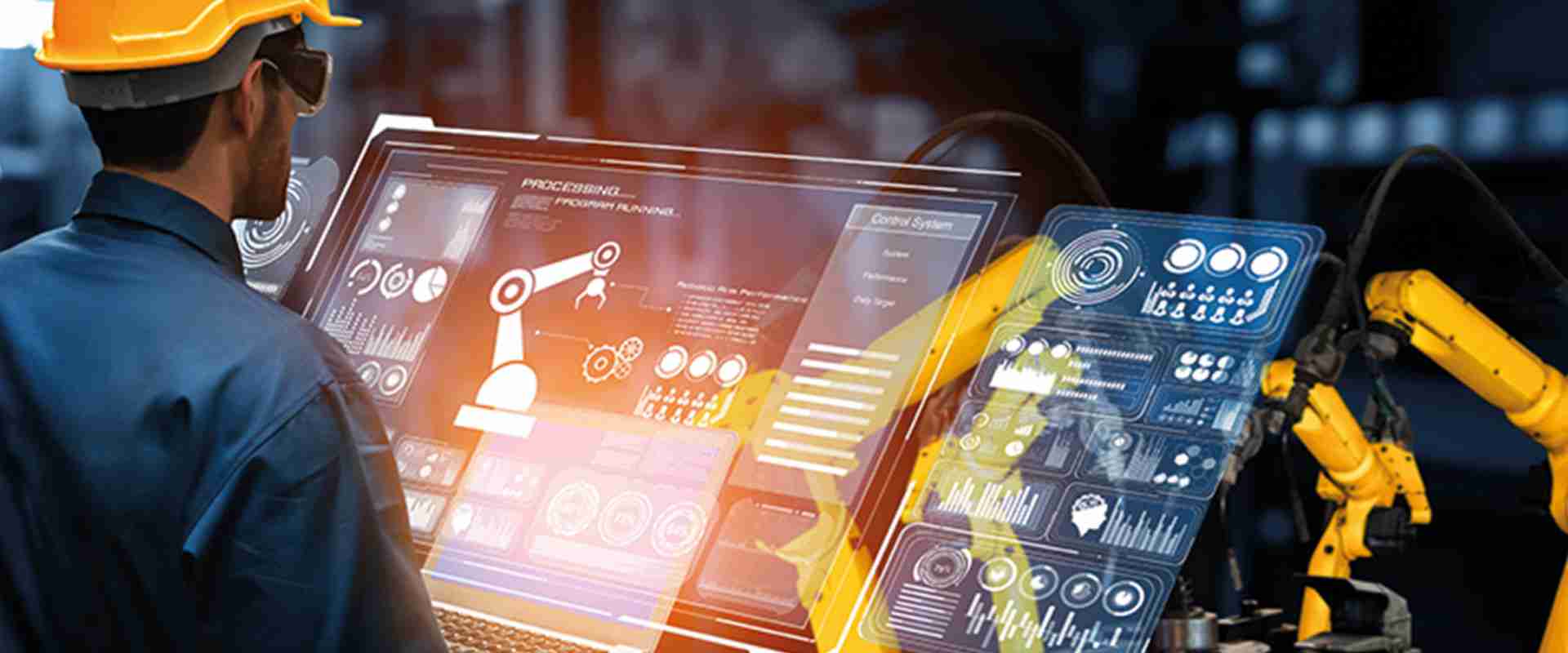
The Industrial Internet of Things brings together analytics, machines, cloud computing, and people to enhance the performance of different industrial processes. Furthermore, with IIoT, companies can transform business models and increase productivity with IIoT. Also, IIoT has continued to play a significant role in digital transformation.

What is Industrial IoT?

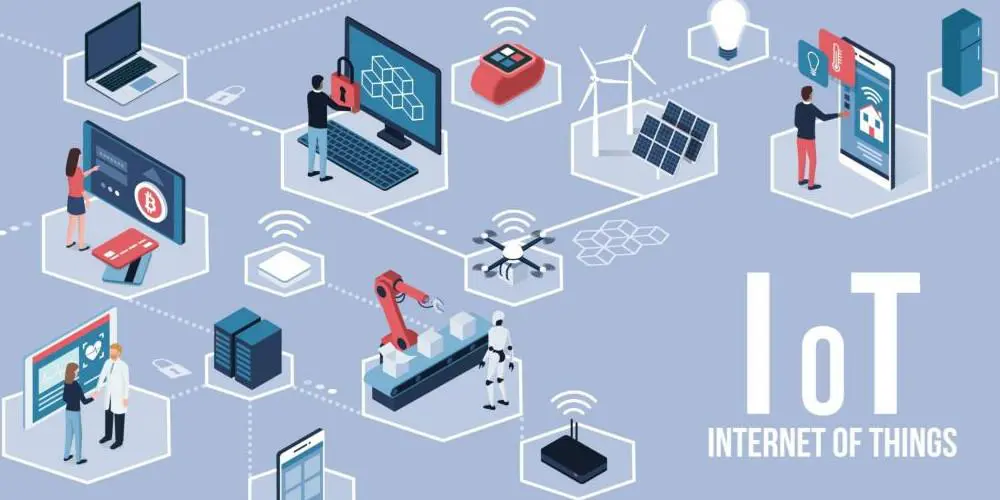
Industrial Internet of Things refers to the integration of IoT in industrial sectors and applications. IoT helps enterprises and industries to operate better. Also, it helps ensure reliability in the operations carried out in industrial sectors. The Industrial IoT comprises industrial applications such as medical devices and robotics.

Furthermore, industrial IoT goes beyond internetworking of devices linked with the IoT. Therefore, one can simply say that the industrial IoT integrates data from sensors and machines to improve industrial processes. Predictive maintenance is one good example of industrial IoT. Also, Industrial Internet of Things is widely used across industries like manufacturing, aviation, transportation, and other industrial sectors.

It covers several industries and applications just like the Internet of Things. Also, Industrial IoT plays a crucial role in converging IT and Ot. Therefore, Internet IoT offers several opportunities in intelligent manufacturing, smart industry, and automation optimization.

Industrial Internet of Things brings together analytics, machines, cloud computing, and people to enhance the performance of industrial processes. Companies can transform business models and increase productivity with IIoT.

The Industrial IoT works just like the Internet of Things (IoT). Internet of Things describes physical objects embedded with software, sensors, and other technologies. These technologies are connected by a network, enabling them to transmit data with other systems and devices.

The operational technology (OT)and information technology (IT) make industrial IoT distinct. OT involves networking of industrial control systems and networking of operational processes. OT and IT convergence offers industries with advanced system integration as regards optimization and automation. Also, it offers enhanced visibility of logistics and supply chain.

The integration of actuators and smart sensors has made the control and monitoring of physical infrastructures in industrial operations easier.

Roles of Industrial IoT Across Major Industries

FULL PCB MANUFACTURING Quote

The Industrial Internet of Things takes a center stage as part of an integrated approach. Also, IIoT is the most important and biggest part of IoT. It plays crucial roles in several industries and sectors.

Manufacturing industry

From an IoT spending perspective, the manufacturing industry is the largest. Manufacturing operations recorded an IOT spending of $102.5 billion. The manufacturing industry is the largest industry in the IoT with an aggregate spend of $178 billion. Manufacturing operations are more than IoT use case investment in several industries. According to the IDC, the maintenance & field service and production asset management are the two important IoT use cases in manufacturing.

Transportation

From an IoT spending perspective, the transportation industry is the second largest market. Also, transportation firms are seeking ways to increase the value chain with monitoring systems and advanced communication enabled by IoT.  The transportation industry spent &78 billion on IoT and this spending will continue to grow.

Furthermore, freight monitoring is the primary use case in transportation. This is great for a large majority of aggregate transportation IoT spend. The increasing emergence of connected logistics reality and a digital supply chain is evident in the overall IIoT evolutions. At the same time these are challenges for transportation and logic market.

Energy and utilities

The energy and utilities market is a major part of the Industrial IoT market. According to IDC, from an IoT spending perspective, utilities are the third industry. Smart grid for gas and electricity accounted for a huge $57.8 billion.

The industrial IoT plays a crucial role in the digital transformation. Smart grids are important in supply and network distribution.

Main Applications of Industrial Internet of Things

Industrial Internet of Things is very important in several businesses. The integration of IIoT is becoming a global trend in businesses.

Predictive maintenance

Predictive maintenance involves identifying the need to maintain a machine before problems occur. If there is any need for maintenance, production will stop immediately. Therefore, it is important to adopt data acquisition, analysis and management system. This system works via sensors that send alerts when some particular risk factors occur.

For instance, the sensors that control robots or the machines that submit data to platforms apply advanced algorithms. These algorithms issue warnings as per vibrations or extreme temperatures that are above normal parameters.

Quality control

Industrial Internet of Things is widely used in monitoring manufactured productsโ€™ quality at any production stage. It monitors the raw materials used, the transportation method, and the reactions of final consumers after receiving the product.

This information is very crucial when applying changes when case failures are identified. Also, the main purpose of quality control is prompt detection of issues in the manufacturing chain. Furthermore, it is crucial to prevent certain risks in industries like food or pharmaceutics.

Automated management of equipment

The automated management of equipment enables a system to remotely monitor and control all company processes. Also, the ability to use digital software and machines to remotely monitor equipment shows that you can control several plants at various geographic locations.

Therefore, this helps companies to monitor advances in their production. Also, companies can analyze historical data they get as regards to their processes. The main goal of utilizing the data is to improve processes and generate an environment that prioritizes information-based decisions.

Other Use Cases of Industrial IoT

Industrial-IoT-Devices
  • Connected logistics
  • Livestock monitoring and smart farming
  • Manufacturing equipment monitoring
  • Asset performance management
  • Energy consumption optimization
  • Smart grid and smart metering
  • Industrial security systems
  • Smart warehousing and smart factory applications
  • Smart logistics and asset tracking
  • Industrial security systems
  • Remote maintenance, field service, and control use cases
  • Smart environment solutions

Advantages of Industrial IoT

Increased operator productivity

Industrial Internet of Things can enhance the manufacturing workforceโ€™s productivity in several ways. Also, operators can work faster without having to compromise quality with the use of IIoT enabled tools. For instance, operators can easily find the piece they want by using the pick-to-light devices. Also, an IoT enabled tool like the torque driver can enhance work adjusting the settings of the tools.

Minimizes quality management systems cost

It is difficult to adopt and maintain the quality management system (QMS). Also, Industrial IoT can minimize the cost of QMS by streamlining and automating the process control plan. With the use of sensors, organizations can check variables that are crucial to quality. Therefore, this reduces the resources and tine needed for QMS. Also, organizations can streamline the process by using IoT sensors instead of performing quality inspections manually.

Improves machine utilization

Industrial Internet of Things helps organizations to link their machines to the internet. Also, this allows organizations to monitor their machines. They can measure critical KPIs like overall process effectiveness and overall equipment effectiveness. Organizations can detect and fix unplanned downtime by tracking these metrics. Also, it could offer preventive maintenance and as such increase the machine use during the operation.

Production visibility

Industrial Internet of Things connects tools, sensors, and machines to offer the needed visibility into production. For instance, organizations can track parts automatically while moving through assemblies utilizing sensors like break beams and RFID. Also, Industrial IoT use can offer plant managers and supervisors a real-time view of the result of their team. This visibility level can help organizations to detect bottlenecks and find the cause of the problems.

Other Benefits of IIoT

Faster improvement cycles

Operators, manufacturing engineers, and process engineers all benefit from industrial Internet of Things. Also, operation engineers will have to collect and analyze data manually without industrial IoT. Therefore, an industrial IoT helps them to automate collection of data.

Ensures predictive maintenance

IIoT devices enables predictive maintenance. Predictive maintenance helps organizations to utilize real-time data from IIoT systems to know when to service a machine. Therefore, this helps to perform the necessary maintenance before failure happens. Also, an organization will be able to achieve improved operation efficiency by addressing maintenance issues on time.

More efficient field service

This is another benefit of IIoT. With IIoT technologies, field service technicians can detect possible issues in equipment before they cause further issues. Therefore, technicians can fix the issue before they become a big problem to customers. Also, IIoT technologies can provide these technicians with vital information about the parts that need repair.

Asset tracking

Asset management systems can help customers, manufacturers, and suppliers to track the condition and location of products. Also, this system helps stakeholders to know if the goods are damaged. The system achieves this by sending instant alert once it detects any damage or risk of damage. Therefore, this helps to adopt immediate measures to solve the problem.

Enhanced customer satisfaction

With IIoT, manufacturers can analyze and capture data on how customers utilize their products. Therefore, this enables product designers and manufacturers to design more customer-centric approach. Also, industrial internet of things offers operational efficiency in manufacturing.

Industrial Internet of Things Enabling Technologies

There are several technologies that enable industrial IoT. These technologies include cloud computing, machine-to-machine, 3D printing, and edge computing. We will be discussing the most important technologies.

Edge computing

This is a computing paradigm that makes computer data storage much closer to where you need it. Also, edge computing is the processing of decentralized data at the edge of the network. Furthermore, the industrial internet needs edge-plus-cloud architecture to improve performance, services, and products in the industrial world.

Cloud computing

You can upload resources and retrieve the internet with cloud computing IT resources and services. Also, you can keep files on cloud-based storage systems.

Radio frequency identification (RFID)

RFID offers a low energy and simple option for connection bootsrapping, and identity & access tokens. Also, this technology integrates a radio transmitter-receiver to track and identify tags related with objects. The integration of RFID technology is very diverse and broad. Also, RFID tags are mainly used to make objects interact with each other. Banking, manufacturing, and logistics are among the industries that integrate RFID IoT solutions.

Cyber-physical systems (CPS)

CPS is the fundamental technology platform for IIOT and IoT. Therefore, it is the main technology that helps to link physical machines that were initially disconnected. Also, CPS incorporates the dynamics of the physical process similar to software and communication. Therefore, it offers design, abstractions and modeling techniques.

Low energy wireless

The major concern for IoT developers is power. Although you can power down sensors and other peripherals for longer time, communications, especially receivers need to remain in listening mode. Also, low-energy wireless extends the lifespan of the device and reduces consumption. Low energy wireless also minimizes the inconvenience and cost of replacing the batteries or the device.

The Major Challenges of Industrial internet of Things

iot-home-devices

The Industrial IoT faces some challenges despite its significant growth. These challenges include:

Data analysis

Data analysis is a never-ending challenge of transferring data to business value. One way to integrate IoT solutions in industrial sectors is to provide tools for data visualization, analysis, and acquisition. These include human-machine interfaces, cloud-based analysis tools, and sensors.

Furthermore, data analysis is crucial in making this huge amount of data generated every minute through rapidly increasing number of embedded systems and sensors.

Lack of skills

Lack of skill is one of the challenges faced by Internet IoT. Inadequate access to the right expertise and skill is a challenge. The skill gap is one of the challenging issues and how to address it. Microsoftโ€™s 2019 Signal report revealed that 29% of organizations hold off on IoT adoption due to lack of resources.

Cybersecurity

One of the major challenges faced by Industrial IoT is how to secure industrial IoT devices. The security problems for Industrial IoT technologies are a major concern as any security breach impacts both organizations and individuals that are prone to operational  efficiency and financial damage. The majority of cybersecurity protection tools mainly focus on cloud and network. However, they miss OTA vulnerabilities. A suitable architecture can help to control security risks. Also, this architecture will ensure that the functionality of the automation system is in cloud or hardened edge computing environment.

Patch management

This is a great challenge as regards IIoT devices. Device manufacturers are now providing periodic firmware updates. Also, organizations need to have a good means of evaluating devices to determine the most recent firmware installed. Furthermore, this kind of tool must work according to maintenance schedule of an organization. This is necessary to avoid disrupting operations.

How to Optimize Industrial Internet of Things Projects

Build partnerships

Collaborations between IT and OT are very important. Also, the business decision makers need to get involved in these processes. Therefore, form partnerships and work with both external and internal parties.

Clarify ROI and business outcomes

Most IoT experts often state that the benefits of the business arenโ€™t clear enough. An Industrial Internet of Things usually begins with an idea, an opportunity or need that is already detected. However, the business case must be clear enough.

Start small

This is a good approach in the Industrial Internet of Things projects. Starting small always gives room to detect failures and amend any mistake.

Security first

Security is very crucial. Also, security by embedded security and design is necessary. It is very important to integrate security as early as possible. You should look at security from a perspective in which there are several components involved.

Architect for analytics

There are data integration problems. It is all about turning data into action, insights, and automation in your industrial IoT project. You will need to utilize analytics to transform data into insights.  

How Enterprises and Industries should Secure the Industrial IoT

Security is crucial in Industrial internet of things. With the use of several sensors and real time data generated, businesses can be more viable when OT connects to the internet. However, the failure to invest in cybersecurity could cause a lot of loopholes. Therefore, security by design and embedded security is critical.

Manufacturers once designed IoT devices without really considering security. Therefore, this resulted in the belief that IoT devices can be insecure. The similarities between IoT and IIoT devices can make one to start considering the safety of IIoT devices. Just like other connected devices, it is crucial to evaluate IIoT devices on a device-by-device.

It is possible the device of a manufacturer is secure while some devices arenโ€™t. Security is of utmost importance among device manufacturers. Some technology companies like IBM, Cisco, and General Electric established the Industrial Internet Consortium (IIC) in 2014. The primary objective of this group is to enhance Industrial Internet of Things adoption. The other working groups of IIC include Industry, Liaison, and Technology.

Security is the greatest risks associated with IIoT. Therefore, IIoT devices keep using default passwords. Many IIoT devices transfer data clearly. This makes interception of data coming from IIoT devices easy. An attacker could can take advantage of insecure IIoT devices and use it to launch an attack.

Security is indeed a very big challenge for people who are in charge of the IIoT devices of an organization. So is device management. It becomes more crucial to implement a great device management strategy if an organization integrates more IIoT devices.

Organizations can identify IIoT devices in order to prevent the utilization of rogue devices. Furthermore, it is crucial to create ways of identifying individual device.

Differences between IIoT and IoT

IIoT and IoT both share some technologies like machine-to-machine communications, sensors, and connectivity. However, they serve different purposes. Internet of Things connect devices across several verticals like healthcare, consumer and utilities. Also, IoT devices comprise fitness bands, smart appliances, and other applications.

On the other hand, industrial Internet of Things offer connection to devices and machines in industries like utilities and manufacturing,. There can be high-risk situations due to downtime and system failures in IIoT deployments. Also, the applications of industrial internet of things are majorly concerned with improving safety or health and improving efficiency.

Also, IIoT offers industrial data. This industrial data is beneficial to industries that depend on IIoT. The automotive industry has witnessed great development due to the impact of IIoT. Furthermore, IIoT has contributed to digital transformation. Providing industrial data and ensuring energy management are crucial for digital transformation. With proper energy management, industries can function better.

What is the Relationship Between IIoT and 5G?

5G is the current standard for mobile networks. Also, it has been designed to offer low latency. 5G feature high data transmission speed. It supports download speeds of about 20 gigabits per seconds. The advent of 5G will impact the utilization of IIoT devices. The low latency as well as high throughput of 5G will enable real time data share in devices.

Before the emergence of 5G, real-time data share was only possible when devices on private networks had high-speed connectivity. Also, real-time connectivity is ideal in use cases like smart cities and driverless cars.

Furthermore, 5G can impact the adoption of industrial internet of Things by resulting in device proliferation. Also, industrial operations might utilize several 5G connected devices. The low latency and high data speed of 5G indicates that IIoT devices are ideal for use in remote locations. Previously, IIoT devices were impractical in these areas due to lack of high-speed connectivity.

IIoT Trends and Future

The future of our industrial Internet of Things follows a trend popularly known as industry 4.0 which means fourth industrial revolution. However, the first industrial revolution, industry 1.0 happened in the late 1700s. Also, this revolution occurred as companies started using stream powered and water-powered machines in manufacturing.

In the early 1990s, industry 2.0 began. Also, the second industrial revolution occurred as a result of the introduction of assembly lines and electricity. In the late 1990s, industry 3.0 occurred and was a result of the utilization of computers in the production process.

Moving forward, we are presently in industry 4.0 today. Also, the fourth industrial revolution was a result of the utilization of connected electronic device, especially IIoT devices. Therefore, industrial Internet of Things devices will impact digital transformations, particularly as some organizations try to digitize heir supply chains and manufacturing lines.

Also, big data analytics will integrate IIoT data. Therefore, this will help organizations to identify changing conditions in real time and act according to results. IIoT devices have been existing for several years; the adoption of real-world is still in the early stage. This will definitely change as 5G become more prevalent. Also, more organization will begin to realize the purpose of IIoT and how it can be of great help.

Conclusion

Industrial Internet of Things helps to ensure predictive maintenance and digital transformation. Also, it helps business models in their supply chain. IIoT plays a significant role across the automotive industry, transportation industry, and more.

Altium Designer 20 Basic Tutorial

Altium Designer 20

The Altium Designer 20 has a whole lot of functionality and features, which includes:

  • Support for rigid-flex circuit board design
  • Routing technology is advanced
  • Powerful reuse tools for design
  • Powerful tools for data management
  • Dynamic intelligence for the supply chain
  • Real-time tracking and cost estimation
  • Flexible management tools
  • Native clearance checking and 3D visualizations
YouTube video

All these functionality is offered through. Also, the whole process of design is performed in one design environment. It is one of a kind, and it is also engineered to offer optimal productivity.

This unified nature of the Altium Designer 20 ensures seamless and easy movement of the design data. This is from a specific design realm to another. However, to start with, the expected learning curve could appear as a strong blockade. This gets to the productivity-enhancing landscape, as well as a whole lot of features that it contains.

Therefore, the main space for the documentation is unique to the Altium Designer 20. This offers the whole information required to help you get started quickly with using the software. Furthermore, from the high-level overviews as well as stepped walk-throughs, and to the complete coverage of the entire resources of the nuts-and-bolts offered via the intuitive interface of the software, this Altium Designer 20 documentation offers you a whole lot of information and knowledge.

Getting Started With PCB Design and the Altium Designer

FULL PCB MANUFACTURING Quote

Is this your first time working with Altium Designer 20 or board design? Are you looking for a place to start? With this Altium designer 20 tutorial, we will reveal to you all you need to know. These include generating the necessary files for the fabrication of bare boards for the 9-component circuit.

This design weโ€™ll be working with in capturing, as well as designing the PCB, is the astable multivibrator. This tutorial will also touch many areas of the altium designer 20 software. With this, you may need to understand properly in your daily design work. This is a great way for you to get used to this software.

Exploring the Altium Designer 20

The Altium Designer 20 has to do with all the software engineers and editors required to perform the development process of electronic products. Furthermore, all the document processing, compiling, and editing is handled in the environment of the Altium Designer 20.

This Altium Designer is twice the integration platform that brings the different functionality and features of the Altium Designer. It also offers a reliable user-interface all through the editors and tools. It also offers further flexibility and the environment is completely customizable. This allows users to set up their workspace the way they work

Also, you will be able to explore the interface and features of the Altium Designer 20, just by experimenting with it. You can also achieve this by creating a new project, and better still, by scanning through the documentation first to help you start ahead.

Extending the Altium Designer

The Installation Management System of the Altium Designer 20 will allow users to handcraft the installation of this software at all times after the initial installation. This will cover not just the updates to the system resources or core functionality, but it can also update, install, or remove the extra functionality. This extra functionality is possible via the optional Extensions available.

The extension is essentially an extra feature to the software, offering the extended functionality and features. A major set of functions and features are handled and installed transparently, which is part of your initial install. This is called System Resources. Furthermore, there are different Optional Extensions. These include optionally removed or installed functionality as required by users.

This is that extension concept, which enables the handcrafting of the installation in line with the design needs. The functionality may add a new exporter or importer. This is a tool that aids the generation of schematic symbol or provides support for a mechanical CAD partnership. To summarize, it is all the targeted functionality packages that enhance and extend the features of the Altium Designer 20

You can get the extensions either as paid subscription or for free. It could also be from Altium or a 3rd party

. Furthermore, with your Altium Developer extension, it is possible to extend the Altium Designer 20 functionality by using the Altium Designer Software Development Kit. This helps you to create your personal extensions for the Altium Designer 20 software.

How the Managed Content Server Works

The managed content server usually works in line with the Altium Designer 20. This is just to offer a good answer to questions regarding the handling of design data using secured integrity.

This server wonโ€™t just offer secure and rock-solid data storage, it also allows data re-release as separate and distinct revisions. This is essentially the changes in tracking design over time. This excludes the need to overwrite the data previously released.

Also, it caters for the entire lifecycle of that data you wish to manage. This allows people that wish to use the data to see at once, the stage of the data. It also reveals what you can use it for safely.

Furthermore, this server is useful in managing the managed data. These include domain models, components, design templates, and schematic circuitry sheets

You can indeed create as well as manage the whole design projects in the server. When you furnish some reusable โ€˜building blocksโ€™ for the design in the server, you will be able to start a new project.

By so doing, you are sure that each component, model, and other design element are now approved and ratified

What are the Preferences of the Altium Designer 20?

PCB Layout in KiCA
PCB Layout in KiCA

The Altium Designer 20 offers the main location whereby you will be able to set up different preferences all through the different areas that are functional on the software. These setting are for the global system and they are applicable across relevant documents and products.

You can perform the preferencesโ€™ configuration from inside the dialog of the preferences. All you need to do is click the control you find on the top right section of the workspaceโ€™ top right. Make use of the options and controls available on your loaded page in configuring what you prefer for that software area

Also, this can be a mix of the satisfying policy of the company policy, as well as the working environment you prefer working in. In addition, the dialog of the preferences offers different tools to make sure that your preferences is just the way you need it. These include:

  • The ability to import the preferences that were defined in an initial instance, or the softwareโ€™s version
  • Ability to save the preferences to, as well as load it from the preference file

Furthermore, if youโ€™ve managed the content server, it becomes possible for you to release your preferences for the Altium Designer 20 formally to the target item in the server

Reference of the PCB Design Rules

The PCB Editor of the Altium Designer 20 makes use of the Design Rules concept in order to explain the designโ€™s requirements. The rules altogether forms a set of instructions that the PCB editor should work with. They include all the aspects of the design, which includes the clearances, routing widths, styles of the routing via, and more. Also, you can monitor a good number of these rules in real-time using the online DRC (Design Rule Checker).

In addition, the design rule targets some objects that are applied in hierarchical form. It is also possible to set up many rules of one type. It could happen that the design object gets covered by two or more rules with a similar scope

For this instance, there is a contention. A priority setting helps in resolving all the contentions. The system passes via the rules from the highest to the lowest priority and then chooses the first one having the scope matching the objects that are being checked.

Reference of the Project Compiler Violations

Compiling is very important in producing an effective netlist for any project. To explain further, it is the compilation process, which yields the designโ€™s data model. This is the dataโ€™s single model, which can be accessed all through the domains of the design in the design environment of the Altium designer 20

You can verify the connectivity awareness in the schematic diagram when compiling according to the rules that are defined as a part of options present in the project. This can be found on the tabs of Error Reporting as well as the Connection Matrix respectively.

The Altium Designer 20 documentation area offers an easy reference that describes every possible drafting and electrical violations, which can result or are present in the source documents during the compilation of a specific project.

Conclusion

We hope you enjoyed and have a good understanding of our article on Altium Designer 20. This unified nature of the Altium Designer 20 ensures seamless and easy movement of the design data from a specific design realm to another.

Top 8 SMD Crystal Dealers In The World

SMD Crystal

Are you in the middle of a design rut requiring crystal units and not knowing which dealer is best to buy from? The best of this type is SMD crystal units. Many dealers worldwide specialize in the production and distribution of SMD crustal units. The choice of the most reliable dealer depends on availability, accessibility, experience, etc. However, thatโ€™s quite a simple task with the following information, highlighting the top 8 global SMD crystal dealers.

River Eletec Corporation

River Eletec Corporation is one of the largest companies dealing with SMD crystal units’ production, development, and sales. The company has its headquarters in Fujimigaoka, Nirasaki, Yamanashi, Japan. In addition, River Eletec has established over 55 operation points globally. The company traces its history in October 1949 as Fuji Sangyo Company but later changed its name to River Eletec in October 1991. The company has established solid associations with one domestic and four overseas companies. Moreover, the company can boast of the ISO9002 certification acquired in September 1999.

Products

The company deals with the following electronic components:

  • Crystal Oscillators
  • SMD diodes
  • Thermistors
  • Crystal resistors
  • SMD capacitors
  • Ceramic capacitors
  • Thyristors
  • Varactors etc

Application of Products

River Eletec Company deals with products applied in the following fields:

  • Manufacture of quartz crystal units such as AT-cut and tuning forks
  • Automotive electronics
  • Audiovisual equipment assembly
  • Wireless communication
  • Internet of Things (IoT)
  • Medical electronics
  • Smartphones assembly
  • Homes automation etc

Market

In 2021, the company’s market capital was approximately 9.80 billion Japanese Yen. Additionally, in April 2022, the company’s working capital was around 80 million US dollars. The company hosts over 195 talented employees, with 50 staff members. With over 55 operation points, the company has a solid global market, with the domestic market occupying the second position in the companyโ€™s market rank.

Nidho Dempa Kogyo Co. Ltd (NDK)

Nidho Dempa Kogyo Co. Ltd (NDK)

In 1948, NDK was initially Nanbu Shoko Co. Ltd. However; the company started the production and sales of SMD crystal units in 1949. Moreover, the company later changed its name to Nihon Dempa Kogyo (NDK) in 1950. Equally important is that the company’s headquarters are in Tokyo, Japan. Throughout the years, the company has dramatically advanced in electronic production and sales. Consequently, the company has established many operation points globally in the Asia-Pacific region (APAC), the USA, and other worldwide locations. Furthermore, dueFurthermore, due to its production of high-quality products, NDK has received many accreditations, such as:

  • ISO9001(1994)
  • QS-9000(1998)
  • Environment system management ISO14001(1999) certification
  • ISO/IEC 17025 (2005)
  • (2014) ISO13485

Products

Being a famous electronic producer and seller, NDK company deals with the following components:

  • Crystal Unit
  • SPXO (Differential Output)
  • Synthetic Quartz Crystal
  • Frequency synthesizers
  • Biosensors
  • Outgas analysis system
  • Crystal Clock Oscillator
  • SAW devices
  • Crystal filler etc.

Application of Products

NDK’s products have a wide range of applications. The following are fields in which the products are relevant:

  • 5G connectivity
  • Automotive technology
  • Network devices
  • Manufacture of watches
  • Digital camera assembly
  • Smartphone fabrication
  • Internet of Things (IoT)
  • Digital consumer electronics
  • Audio visual systems
  • Personal computer fabrication etc.

Market

The company has established solid and improved worldwide investor relations, leading to its relatively large working capital. Additionally, the many global operation points ensure a comprehensive client population coverage, creating a solid international market. On the other hand, the domestic market takes a lower proportion, occupying the second position. Nevertheless, the company’s well-established online marketing platform cuts across the two market types.

Mercury Crystal Electronic Company Ltd.

FULL PCB MANUFACTURING Quote

Founded in 1982, the company has 40 years of experience producing and selling SMD crystal units. Its headquarters are in Taiwan. Despite having made SMD crystal Units for 40 years, the company’s products have considerably evolved from the old designs. Moreover, they have modified their packaging style from lead type to surface mount type. Additionally, the frequency range has increased from Several kilohertz (kHz) to hundreds of megahertz (MHz).

Consequently, the precision calculation has changed to parts per million. In addition to the headquarters, the company has established many other operation points worldwide. Moreover, Mercury Crystal has over 30 functional global labs. Furthermore, the company works towards providing a healthy and secure working environment for its more than 500 workers, hence increasing their productivity. To avoid energy and resource losses, the company implements the ISO14001 certification.

Products

Mercury Crystal company deals in the production and sale of the following products:

  • Quartz crystal
  • Crystal filters
  • VCXO
  • Clock oscillators
  • TCXO/VCTXO
  • OCXO etc.

Application of Products

The companyโ€™s products are applicable in such fields as:

  • Automotive electronics
  • Consumer electronics
  • Communication development
  • Industrial Electronics
  • Computing and automation
  • Internet of Things (IoT) etc.

Market

With its headquarters in Taiwan, the company’s domestic market is in the Asia-Pacific (APAC) region. However, the numerous operation points facilitate a more solid global market. Additionally, the company’s research labs allow for the designing of more developed items, attracting many end clients globally. Consequently, the company has a competitive advantage over similar companies.

Abracon

abracon

Founded in 1992, Abracon is a leading producer and supplier of electronic circuit components. The company’s main office was initially in Irvine, CA, but later relocated its headquarters to Spicewood, TX, at the center of Texas Hill Country, Near Austin. Moreover, the company remains a private but highly excelling company. Abracon is a high-quality supplier of SMD crystal units with one of the highest customer counts in the world. Furthermore, the company has established solid associations with many other similar companies worldwide, helping it study the competitors’ trends and strong points. Equally important is that the company actively supports the ECIA PACE Training Program. The program offers its employees and member companies key industrial concepts.

Products

Abracon is a famous dealer in such products as:

  • Quartz oscillators
  • XO
  • TCXO
  • MEMS
  • Resonators
  • Real-Time Clocks
  • VCXO etc.

Application of Products

The companyโ€™s products offer electronic solutions in the following fields:

  • Automotive electronics
  • Consumer electronics
  • Industrial Electronics
  • 5G facilitation
  • Internet of Things (IoT)
  • Medical electronics etc.

Market

Abracon can boast over 25,000 active customers in both the domestic and the global market. Moreover, as a largescale producer, the company records an annual overseas shipment of over 600 million parts. Furthermore, the US end clients make up the company’s solid domestic market. Additionally, the company’s flexible supply chain enables it to deliver to its clients through the most modern means. The company’s talented engineers help maintain its reputation due to their high-precision goods. Consequently, the company has a competitive advantage over its competitors.

Rayming Technology Company Ltd.

Founded in 2005, the company is one of the leading SMD crystal producers and suppliers in China and also globally. Raymingโ€™s headquarters are in Shenzhen, Guangdong, China. Moreover, through the years, RayMing corporation has established the QS9000 and ISO9001 quality system certifications. Customer satisfaction is guaranteed by the two. Since more customers get attracted to this confidence, the market size grows. The business can also take pride in an upgraded quality assurance system and other quality inspection tools. By assisting in monitoring the entire production process, the device gives the retailers confidence in the stability of the product. Moreover, Rayming corporation has held membership with ECPlaza since 2014.

Products

The company also deals with other circuitry components besides SMD crystal units. These components include:

  • SMD resistors
  • ceramic capacitors
  • thick and thin film capacitors
  • SMD diodes
  • wireโ€“wound resistors
  • inductors
  • switches etc.

 In addition, RayMing tech also deals with the manufacture and assembly of printed circuit boards (PCBs).

Application of Products

Raymingโ€™s products have a wide range of applications. The following are some of these applications:

  • Automotive electronic connections
  • Industrial Electronics
  • Consumer appliances
  • Internet of Things (IoT)
  • Telecommunication electronics
  • Space surveillance systems
  • Smart homes
  • Building automation etc.

Market

The profit-driven RayMing corporation exports its goods all over the world. The domestic market in the Asia-Pacific region makes up the primary market. The domestic market generates the rest of the demand. Additionally, the company’s primary market target is the USA and Europe. The company’s employees work to provide high-quality goods that will help the market grow and result in increased profit. Furthermore, the company’s developed online selling platform offers a solid worldwide market to the company.

Crystek Corporation

Crystek Corporation

Founded in 1958, Crystek is among the world’s best SMD crystal unit dealers. The company is privately owned and has its headquarters in Fort Myers, Florida, United States of America. In addition, the company deals in producing and selling frequency control solutions and RF microwaves. More precisely, the company has unique expertise in SMD crystal units. Additionally, the company has established numerous operating points and branches worldwide. Also, the company can boast over 50 functional research labs globally.

Furthermore, Crystek holds the ISO9001 (2015) certification of quality management. Consequently, their products are of reliable and effective quality. In addition, the company hosts over 450 employees in all its stations, with over 120 staff members. Crystek has also established a solid connection with similar companies that act as market surveillance and study platforms.

Products

Crystek company deals with the following components besides SMD crystal units:

  • Temperature Compensated Crystal Oscillators (TCXOs)
  • PLL (Phase Lock Loop)
  • RF power detectors
  • Attenuators
  • RF coaxial cable accessories
  • Synthesizers
  • Quartz-based resonators
  • Connectorized amplifiers
  • Power regulators etc.

Application of products

Crystek company’s products have relevance in the following fields:

  • Telecom systems
  • Industrial Electronics
  • Aerospace technology
  • Microwave/radio systems
  • Wireless transmission systems
  • Antenna receivers
  • Medical electronics etc.

Market

Owing to its advanced research labs and skilled personnel, Crystek produces high-quality, reliable products. Consequently, the company gets a competitive advantage over similar companies, boosting the company’s market. Furthermore, its certification helps in building a robust reputation, attracting more clients as a result. Governmental bodies are the company’s leading domestic market, with the online platform connecting it to its global market.

Micro Crystal AG company

 Founded in 1978, Micro Crystal company has its Headquarters in Grenchen, Switzerland. Additionally, the company is a long-time member of the Swatch Group Inc. Moreover, the company is a renowned SMD crystal unit and tuning fork watch crystals. Micro Crystal is among the leading producers and suppliers of SMD crystal units, and Miniature Quartz Crystals range between 30KHz and 250 MHz. Furthermore, the company facilitates the fabrication and testing of new electronic ideologies, allowing for an up-to-date distribution system. The company has numerous well-established operating points globally, with over 40 operational research labs.

Products

Micro Crystal company deals with the following products other than SMD crystal units:

  • kHz Oscillators
  • Real-Time Clock modules (RTC)
  • High-frequency crystal
  • Whitepapers and LCDs
  • Temperature Compensated Crystal Oscillators (TCXOs) etc.

Application of Products

Micro Crystalโ€™s products have a wide range of relevancies in such electronic fields as:

  • Medical implantable electronics
  • Consumer appliances
  • Industrial Electronics
  • Automotive electronics
  • Internet of Things (IoT)
  • Telecommunication
  • Marine electronics etc.

Market

Due to the many operating points, the company has a solid global market. Moreover, Micro Crystal has shipped more than 500 million SMD crystal parts to over 200,000 customers. Additionally, the company’s domestic Swiss market occupies the second market rank. Furthermore, Micro Crystal company offers superb after-sales services to its customers and a ready client consultancy to achieve a competitive advantage over similar firms.

Aker Solutions

Aker provides integrated and developed circuit solutions to electronic engineers worldwide. Consequently, the company boosts the global energy industry. Aker company traces its history to 1841 in Oslo, Norway. Therefore, the company has 181 years of existence and experience. In addition, the company has over 53 well-established branches and operation points and over 20 global research labs. Furthermore, the company started as a small workshop, Akers Makeniske Versted, near the Aker River. Later, the company grew steadily, first into shipbuilding and then a stable engineering company.

Products

Other than SMD crystal units, the company also deals in the following products:

  • PLL (Phase Lock Loop)
  • RF power detectors
  • Attenuators
  • RF coaxial cable accessories
  • SMD capacitors
  • Antenna receivers etc.

Application of Products

Akerโ€™s products are relevant in the following fields:

  • Telecommunication
  • Positioning systems
  • Automotive electronics
  • Internet of Things
  • Consumer appliances
  • Industrial electronics
  • 5G modulation systems etc.

Market

With over 14000 employees, the company is among the largest SMD crystal dealers in the world. Consequently, the company manufactures and then supplies its SMD crystal units and other products to a vast global market via air or water. Moreover, the price of a single share is approximately 34.92 US dollars. The company’s developed products accord it a competitive advantage over fellow firms.

Conclusion

The above information makes it possible to understand the best SMD crystal dealers in the world. Moreover, it gives a short history of each dealer company, including the year the company and the location of the companyโ€™s establishment. In addition, the information clearly explains the current day headquarters of each company. Furthermore, the range of products dealt with by each company, and their applications, are no longer an issue with the above information. Finally, the information examines the market specs of each of these eight companies. In conclusion, the above information equips you with the knowledge on which SMD crystal company to consider for your research.

Top 12 Industrial Robot Manufacturers in the world

Robots in Industries

Industrial robot manufacturers design, produce, install, and maintain these systems. In addition, they provide the physical robot, the computational interface, and guidance on integrating the system into the existing manufacturing space.

Some industrial robotics manufacturers produce their components, while others outsource specific parts. These machine automation suppliers typically produce specialized robots for applications, while generalized robots can serve in several manufacturer-designated roles.

In the end, the ultimate purpose of industrial robots is to enhance productivity and quality in manufacturing environments.

Industrial robotics companies often provide customized robot solutions for specific industries, such as car manufacturing. In addition, some industrial robotics companies, like Denso, specialize in various applications.

Others, like Kuka, are innovative and have launched new designs in their field. Some companies, like Toyota Motor Company’s Kuka, have roots in the automotive industry, while others focus on manufacturing industrial robots.

Midea, for example, is a sprawling conglomerate that owns a robotics division, which has nothing to do with its automotive division. Mitsubishi, meanwhile, has become one of the world’s largest industrial robot manufacturers.

What Makes a Leading Industrial Robot manufacturer?

When choosing a robot, you have several key features to consider. A top-quality industrial robot should include the most advanced technology for the application. It should also be easy to maintain and safe to use. For example, controller specifications are essential to an industrial robot’s success.

Its memory capacity, human-machine interface, and internal sensing capabilities are essential. Each robot has a unique requirement and may require different controller specifications.

For example, a simple pick-and-place application may require the essential software, whereas a high-precision manufacturing application requires sophisticated software and a more complex controller.

The Benefits of Industrial Automation in robotic automation systems

Industrial automation can increase your productivity and efficiency. The advantages of automation are many, and the initial costs are low. Unlike human operators, robots can save time, money, and effort.

They can also help you reduce waste and improve quality. In addition, robots can improve your speed to market and reduce lead times. Additionally, automation can even make in-house production more affordable. In other cases, industrial automation systems can help you increase your profit margins.

One of the best things about industrial automation is that it can reduce employee costs. Using industrial automation can free up human workers to perform more complex tasks. As a result, you can eliminate the need for healthcare benefits, paid holidays, and more.

Moreover, workers do not need to worry about the maintenance of industrial automation machinery, which saves you money on wages. However, you must be careful not to sacrifice quality in the process, as industrial automation is highly repeatable.

Top Industrial Robotics Manufacturers around the world

These industrial robotics companies are developing new industrial robots to help businesses operate more efficiently.

Read on to learn about these innovative companies and see what differentiates them. You might even be surprised that KUKA invented the robot called the Kukabot.

KUKA

KUKA has been at the forefront of industrial robot design since the early 1970s. They released their first industrial robot, the Famulus, in 1973. It was the first industrial robotย companyย with six axes powered by electric motors.

KUKA continued to push the boundaries of industrial robotics in 1985 with the introduction of their Z-shaped robotic arm, which allowed for six degrees of freedom and simplified maintenance. By the late 1980s, they were leading suppliers in Europe and the United States.

KUKA is a global automation corporation with over 3.3 billion euros in annual sales and more than 14,000 workers. The company has subsidiaries in Asia and Europe and is one of the leading providers of intelligent automation solutions.

The company provides complete automation solutions for a variety of different industries. Its robots help increase productivity and reduce costs for various businesses. In addition to manufacturing robots, KUKA also designs and builds software to improve productivity and efficiency.

KUKA offers flexible manufacturing systems for many industries, including automotive and rail vehicles. Its products are ideal for mounting vehicle bodies and chassis, installing components, and more.

Its customers include GM, BMW, and the BSH rail vehicle manufacturer. KUKA has also set up innovative production lines for freight wagons, subways, and locomotives. In addition to robotics, Kuka also provides services and solutions for various industries, including the food and beverage industry.

TAL

The report is a comprehensive list of the top companies in the industrial robot industry, and it also lists the top companies in the service robotics industry. This list includes companies like ABB Ltd., Fanuc Corp., and Kawasaki Robotics.

These companies offer industrial robot solutions that are highly customizable and customized to suit the needs of specific industries. In addition, these companies have years of experience in the industry, and they are considered one of the top industrial robot manufacturers.

The global industrial robotics market is currently in two parts – the European and the North American sectors. Unfortunately, the two regions saw a significant decline in revenue in the first two quarters of 2020.

The impact on service and collaborative robots will be more limited, as their growth rates are higher than those of industrial robots. However, the APAC region has a much higher growth rate.

FANUC

FULL PCB MANUFACTURING Quote

In the US, FANUC is the largest industrial robotics company, with more than a hundred models of robots and intelligent automation systems. Its revenue is diversified, with 15 percent coming from Japan, 21 percent from the Americas, 19% from Europe, and 33% from Asia, excluding China. As a result, it can serve any industry with standardized processes that justify robot installation.

The company has been in business since 1892 and has a presence in more than 100 countries. Its mission is to make the future a better place by providing the latest technology and out-of-the-box thinking.

It has become a leader in industrial robotics and uses more than 400,000 robots. Its products are renowned for their durability and ease of use and are ideal for various manufacturing processes.

Yaskawa Electric

To invest in industrial robots, you should consider the following manufacturers: Comau Robotic Systems, Yaskawa, and Kuka. These companies have a history of providing innovative industrial robots, ultra-precision machines, and robotic systems.

The MZ12 industrial robot, for example, is designed to carry up to 12 kilograms. In addition to its strong market position in the electronics and EMS industry, the company also manufactures other industrial robots, such as the Compact MZ Series, WING SLICER Type EZ Series, and FlexGui.

Japan’s economic miracle began to unravel after the country’s housing bubble burst in 1991, and the economy stagnated for the next two decades. However, the sudden rise of personal computers spurred an increase in the demand for semiconductors, a key component for industrial robots.

The global market for industrial robots remained strong until the 2008 Great Financial Crisis. The country’s supply of industrial robots declined significantly after the 2011 Tohoku Earthquake.

Another Japanese company, Yaskawa electrics, has a history of manufacturing industrial robots. The company’s main products include servos, AC motor drives, and motion controllers.

The Motoman industrial robot is one of the most well-known industrial robots on the market, with more than 400,000 installed worldwide. Yaskawa also makes cobots, welding robots, and materials handling robotic arms.

Omron industrial robots

arm-Robots-

The company has five innovation centers throughout the world. Its products have been essential in more than 120 countries. So, what makes a leading industrial robot brand? First, let’s take a closer look at some of the most well-known brands in this industry.

Automation is becoming an increasingly popular option for many industries, but the cost of labor and COVID-19 concerns have created an even greater need for collaboration and automation. As such, OMRON has invested in Techman Robot Inc., the second largest manufacturer of collaborative robots.

Upon completion of the deal in December 2021, Omron will hold a 10% stake in the company. Demand for collaborative robots is increasing as workers look for cobots – robots that can work alongside humans, handle multiple tasks, and ensure safety.

Omron, an industrial automation company, based in Kyoto, Japan, has been in the robotics business for over 30 years. Its innovative robotic systems include the Parallel Link Quattro robot, a two-armed industrial robot.

The company has been working to advance its robotics and software technologies for years. A recent Adept acquisition by Omron enabled it to provide automation for multiple industries, including medical and automotive. Omron also has an extensive business in components and sensors for industrial robots.

It is also widely considered one of the world’s first collaborative robot manufacturers. Omron’s robotic solutions make integration easy. Their automation solutions offer flexible, modular programming and SQL connectivity. Omron is a global robotic manufacturing leader with more than 37,000 employees.

Another innovative product from Omron is the Factory Drive Recorder. This innovation lets engineers record videos of key production events. This feature makes it easy to identify quality problems and improve processes. Omron is one of the ten industrial robot companies that lead the industry

Staubli

As one of the top mechatronics solution providers worldwide, Staubli Group excels in three main areas: textiles, robots, and software solutions. Since its founding in 1892, Staubli has grown geographically and technologically.

Its acquisition of Unimation expanded its portfolio into some of the most advanced industrial sectors. In addition to industrial robots, Staubli has also expanded its software business to offer a range of collaborative robots, and the company has recently invested more in its software business.

Germany leads the way with a strong presence in the industrial robotics market. Its industrial robotics division serves the automotive, electronics, logistics, and consumer goods industries. Its six-axis robots include ones with dirt resistance and palletizing capabilities.

It was acquired by the Midea group in 2016, enabling the company to diversify its product offering. Another company leading the way in robotics is Staubli. Based in Horgen, Switzerland, Staubli’s business has grown to more than $1 billion.

Epson Robots is a Japanese company that produces industrial robots. Based in California, Epson Robots has 35 years of experience manufacturing industrial robots. The company is also the world’s leading SCARA robot manufacturer.

Staubli Corporation is a global mechatronics solution provider with operations in 29 countries. With its flexible robotics solutions, the company is one of the top 10 industrial robot companies that lead the industry.

ABB Robot Systems

ABB robotics creates flexible and adaptable machines that can perform multiple tasks. The GoFa collaborative robot, for example, can handle larger payloads. In addition, its collaboration with humans eliminates physical barriers, allowing continuous workspace sharing and cooperation.

Its lead-through programming makes it easy for non-experts to program it, and it is ABB Wizard’s easy programming software that helps users program the robot with graphical blocks.

ABB is a leading manufacturer of industrial robots, with over 300,000 units installed in over 53 countries. The company also offers information technology services, a competitive edge over other industrial robot manufacturers.

Yaskawa, a Japanese manufacturer, was founded in 1915 and has since evolved from a motor manufacturing company into a world-class robotics manufacturer. Its products span virtually every industrial sector.

EPSON Robots

EPSON Robots is the robotics design division of Japanese corporation Seiko Epson, the company that makes computer printers and watches. The company is focusing on developing a fully autonomous robotic arm for the future.

While it is unclear when the robot will be ready for market, it has shown promising signs for the future. In the meantime, it has several projects, including autonomous walking and navigation.

Kawasaki Heavy Industries

Kawasaki robotics is one of the oldest companies in the industrial robots industry. In 1969, the Japanese company developed the first industrial robot. It continues to produce quality industrial robots to this day. It is the top industrial robot manufacturers’ sector and regularly surprises the world with innovative innovations.

To help humans, Kawasaki Heavy Industries has been working on humanoid robots. For example, in 2017, the company unveiled the humanoid robot Kaleido. Kaleido will be more humane and valuable in human society.

Kawasaki shared details about the robot’s progress at the International Robot Exhibition (iREX) 2019, held at the Tokyo Big Sight from December 18 to 21. And if you’re looking for a brand with a long history, Kawasaki is a must-have.

Mitsubishi Electric Corporation

Mitsubishi Electric Corporation is an internationally recognized electrical and electronics manufacturer with a long list of products. While most robots manufactured by this company are white, those manufactured by this company consist of distinctive branding and product design.

For instance, robots manufactured by ABB are white with a red logo. RoboDK is a global company that provides solutions to industrial robotics problems and supports them.

Doosan

Doosan, a major South Korean company interested in almost every industry, is also a leading industrial robotic manufacturer. Moreover, this company has recently launched new types of industrial robots for the electronics industry, which is growing faster than the automotive industry.

Meanwhile, Denso is known for its car parts, a Japanese brand that has frequently appeared at Hannover Messe. With all these advantages, it’s no wonder that Toyota has acquired a leading industrial robot brand.

Nachi Fujikoshi Corporation

To understand the company’s products better, consider the following information. What makes Nachi-Fujikoshi Corporation different?

The Nachi-Fujikoshi Corporation is a major Japanese corporation that manufactures a range of machine components, systems, and industrial robots. Its other products are known for their innovative manufacturing and assembly process solutions.

Summary

Robotics is a rapidly growing industry, and the need for companies that manufacture these machines is as great as ever. Since their first use in the 1960s, robots have come a long way.

They are now less expensive to buy and install than ever, and their quality and safety standards have improved. They can also operate twenty-four hours a day, seven days a week, which increases production and decreases downtime.