What is the Significance of Azure IoT?

Azure IoT

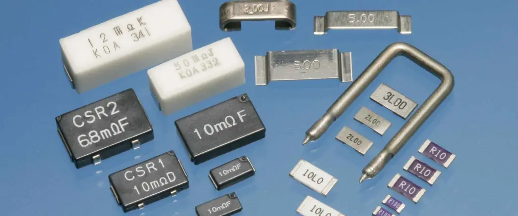
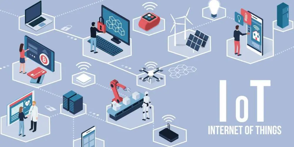
A system of physical objects known as Internet of Things or IoT connects to and exchanges data with some other objects and services across a network, be it the web or another one. Currently, there are more than ten billion linked devices in use worldwide, and this number keeps growing. The internet can be used to connect anything which could be implanted with the required software and sensors.

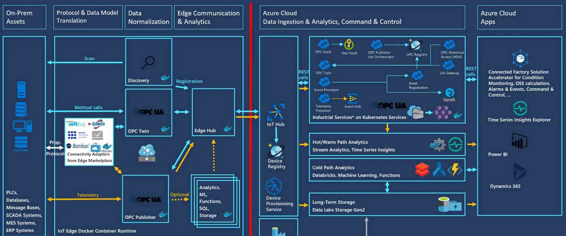
The IoT application as well as the connected devices uses the managed Azure IoT Hub service, which is hosted within the cloud and serves as a centralized messaging hub. Numerous devices as well as their backend programs can be securely and reliably connected. The Azure IoT hub can be linked to almost all devices.

What is Azure IoT Hub?

A group of cloud services managed by Microsoft known as the Azure IoT connects, keeps track of, and manages countless IoT assets. A IoT solution, to put it simply, consists of at least one IoT device that connect to at least one back-end service that are stored in cloud.

Microsoft’s IoT cloud connector is called Azure IoT Hub. Many IoT devices may communicate reliably and securely with a specific solution back end with this managed service.

You may learn about the condition of your assets and devices using device to cloud telemetry data. You can send commands as well as notifications into your linked devices via cloud-to-device messaging. Device communications are transmitted in a sustainable manner to support devices attached and disconnected at different times.

Device-to-cloud telemetry, file uploading from devices, as well as request-reply techniques to manage the devices from off the cloud are just a few of the messaging patterns that are supported. You can track the creation, connections, and failures of devices with the aid of monitoring, which is supported by the Azure IoT Hub.

To serve your personal IoT workloads, IoT Hub expands to many devices connected at once and many events per second. Read on the scaling of Azure IoT Hub for additional details on how to scale your Azure IoT Hub. Visit its pricing page to find out more regarding the IoT Hub service tiers.

Applications of Azure IoT Hub

FULL PCB MANUFACTURING Quote

The Azure IoT Hub can be integrated with other services from Azure to create comprehensive, all-encompassing solutions. Use Event Grid, for instance, to help your company respond to urgent situations in a secure, scalable, and reliable way.

To help automate business operations, use Azure Logic Applications. To add AI models and machine learning to any solution, use the Machine Learning by Azure.

To do real-time analytical computations on your streaming of data from these devices, use the Stream Analytics of Azure. Numerous Iot hubs are utilized by IoT Center applications included among their resilient and scalable infrastructure.

To avoid service misuse, default quota restrictions are set for every Azure subscription. The idea of an IoT solution might be impacted by these restrictions. 50 Azure IoT hubs are currently the maximum allowed for every subscription. You may ask for quota increases simply by getting in touch with support. Read IoT Hub Throttling and Quotas for more details.

What to Consider when Getting Started with Azure IoT

  • Understanding the development paths of the device,
  • Selecting hardware,
  • Choosing a service to help in device connection
  • Selecting the SDK
  • Tools to help in connecting and managing devices

Development Paths of a Device

Two typical device development routes are covered in this article. A selection of tasks and development possibilities are included for each path.  

Development of device applications: Complies with current best practices, focuses on the higher-order languages, as well as runs on the operating general purpose system like Linux or Windows.

Development of embedded hardware explains resource-constrained device development. It’s common to employ a resource-constrained device to cut prices per unit, power usage, as well as device size. Such gadgets have complete control over any hardware environment in which they operate.

Development of device applications

Industrial-IoT-Devices

Existing devices are being modified by developers of device application so they may connect onto the cloud or just be incorporated into IoT systems.

These devices frequently support a powerful general-purpose operating system like Linux or Windows and can support some higher-order languages like Python or C#. Containers,  PCs, Raspberry Pis, as well as mobile devices are typical targets.

Developers of device applications concentrate on allowing an IoT situation required by a cloud solution rather than creating constrained gadgets at scale. For the cloud solution, some developers would also operate on restricted devices. See Embedded Device Path of development if you are a developer dealing with devices that have limited resources.

Developing embedded device

Targeting constrained devices with little memory and computing power is embedded development. What could be accomplished is limited compared to the conventional development platform by constrained devices. Real time operating systems or absence of operating systems is often used by embedded devices.

Because they don’t have a general-purpose operating system, embedded devices possess complete control over the hardware. Because of this, embedded devices are an excellent option for the real-time systems.

Furthermore, the C language is the focus of the present embedded SDKs. These embedded SDKs support Azure RTOS or don’t support any operating systems at all. With the embedded targets kept in mind, they were created. The requirement for a small footprint as well as non-memory allocation design is known as the design considerations.

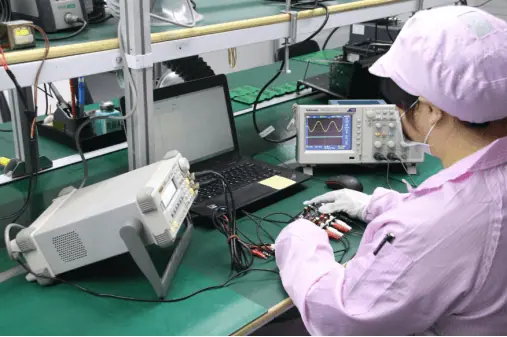
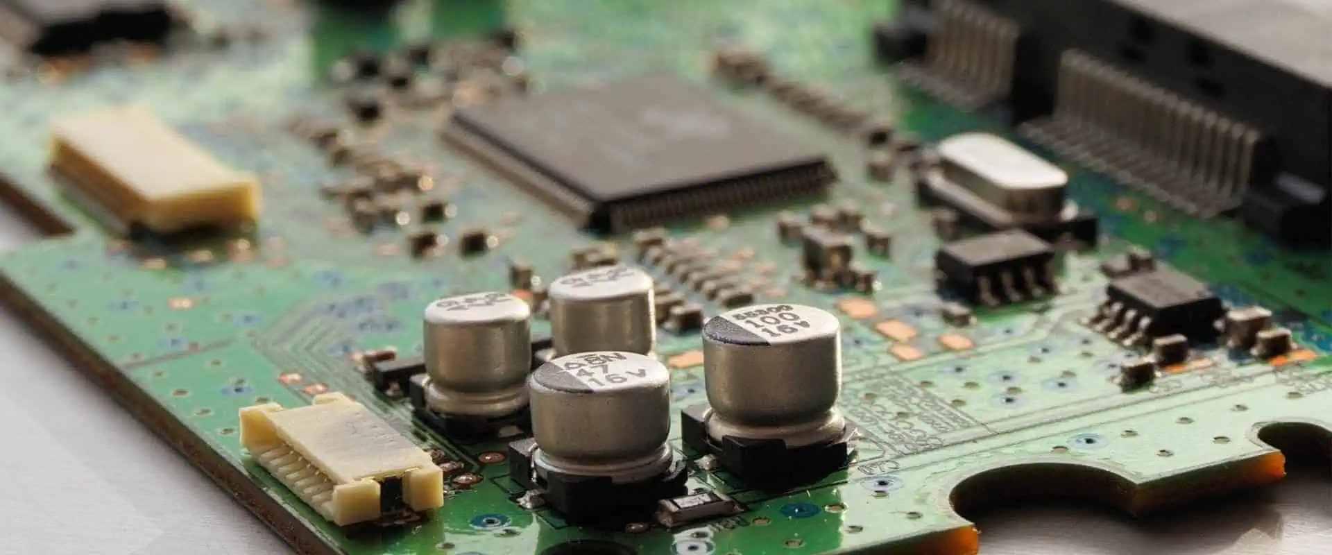
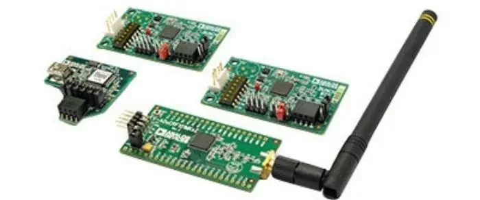
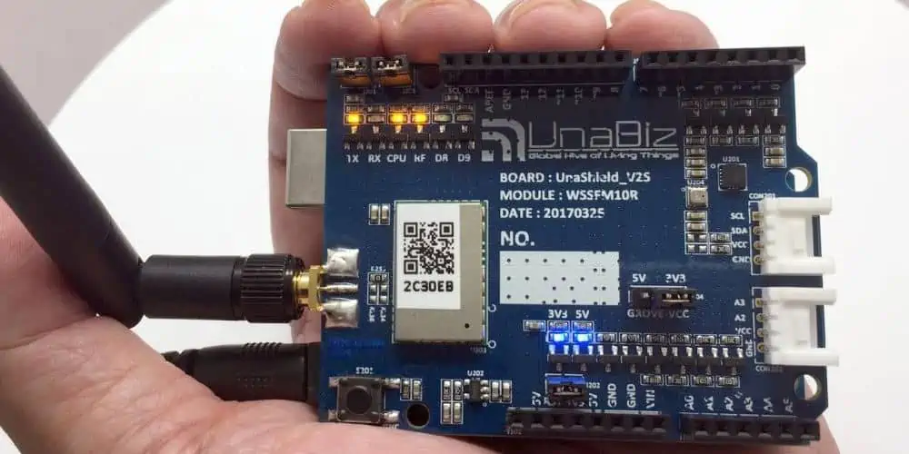
Selecting your hardware

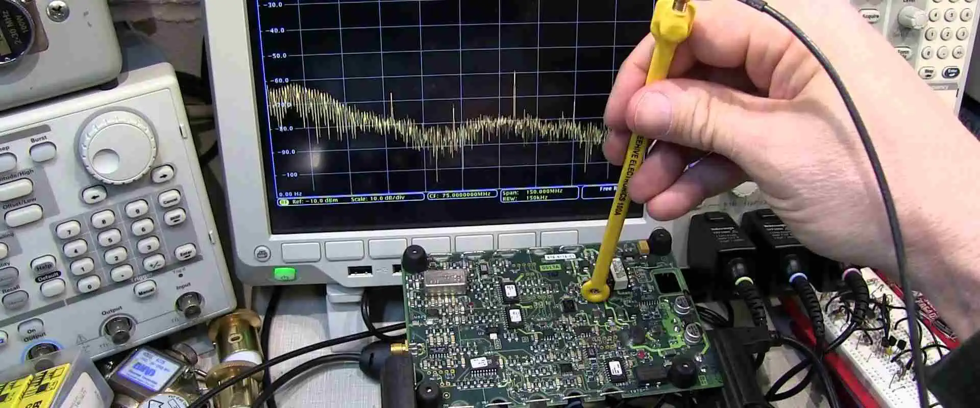
The fundamental elements of the IoT system, the Azure IoT device is in charge of watching and communicating with their surroundings. IoT devices come in a wide variety of forms, so it’s important to comprehend what they are as well as how your development process may be impacted by them.

Selecting an SDK

You have access to a wide range of SDKs as the developer of the  Azure IoT device can assist you in creating cloud applications that support devices. The SDKs remove a lot of complexity involved in the connection as well as management of the devices and streamline the development process.

For the creation of devices, there are about three main IoT SDKs. Device, embedded device, as well as service SDKs are all ways to connect current general-purpose devices into Internet of Things applications utilizing the higher order language. The service SDKs helps in creating Azure IoT solutions which connects the devices to different services)

Choosing a service

The choice of a service that your devices will connect to can be described as an important stage in the process of development. IoT Hub as well as IoT Central are the two main Azure IoT solutions for managing and connecting devices.

Azure IoT Hub:ย This is useful in linking devices and host different IoT applications. A PaaS program called IoT Hub serves as the central messaging node for two-way communication between linked devices and IoT applications. Millions of different devices can be supported by IoT Hub at scale. The IoT Hub gives you the most power or customization over the design of your application when compared to the other services rendered by Azure IoT. With some increase in administration and development complexity, it also provides the most possibilities for dealing with the service’s developer tools.

Azure IoT Central Working with different IoT solutions will be made simpler by IoT Central. It serves as the proof of concept for testing the IoT solutions.

Advantages of the Azure IoT Hub

Safe communication between different devices is made possible. Secure channels are assigned by Azure IoT Hub for the data transfer between your apps and devices. In order to guarantee that every device could be linked to and maintained securely, it offers you per-device authentication.

Additionally, Azure IoT Hub offers the amazing device positioning, which enables you to assign any IoT device towards the appropriate Hub when it is enabled. Above all, the Azure service offers you a variety of authentication options for multi-device functionality. Some authentication types that are accessible are:

  • Token-based SAS authentication
  • X.509 individual certificate authentication
  • CA X.509 CA Authentications

Customizable Routing Message Functionality

You can set up rules-based messages automatically using the flexible message route functionality provided by Azure IoT Hub. The following are some of the features:

  • Routes messages through multiple endpoints
  • Uses the Azure IoT Hub to direct device telemetry towards particular endpoints
  • Simple creation and assignment of no codes routing rules

Seamlessly Connect the Azure IoT hub to additional services

The Azure IoT Hub’s ability to be integrated with other Microsoft Azure services is its third significant advantage. Stream Analytics, Machine Learning, Event Grid, and Logic Apps are a few of the services rendered.

Highly available

One major feature of the platform is Azure IoT Hub’s 99.9% SLA for uptime for all users.

Conclusion

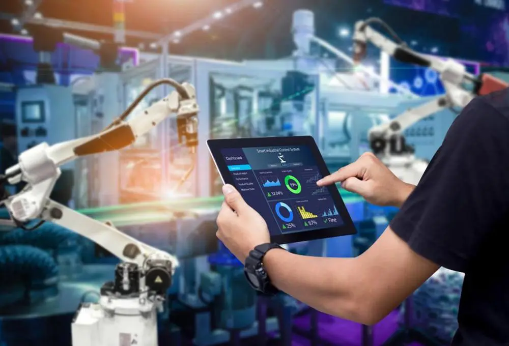
When it comes to handling and analyzing the enormous data that comes from IoT devices used in your company, Azure IoT hub could save you time. Just like the internet, IoT has the potential to transform the world. Azure IoT Hub could be a terrific solution to simplify your life when your company now employs or intends to utilize the IoT power.

Why RFT Testing is Crucial in Ferromagnetic Tubes Inspection

RFT Testing

There are several difficulties encountered during ferromagnetic tubes testing. The remote field testing (RFT) can help to alleviate these difficulties. The RFT testing method offers a lot of benefits, one of which is allowing almost equal sensitivities of detection at the external and internal surfaces of a ferromagnetic tube. Also, this testing method is known to be sensitive to changes in wall thickness. It is not very sensitive to fill-factor changes between the tube and coil.

What is RFT Testing?

RFT means remote filed testing. It is a testing method carried out on ferritic materials. These materials make use of alternating current to cause an electromagnetic field. The remote field testing is a reliable method of testing ferritic materials.

Remote Field Testing is an electromagnetic testing method that discovers discontinuities ferromagnetic (Carbon steel) tubes and pipes. RFT is a through transmission test method in which the receiver coil discovers electromagnetic field that traversed via the tube wall. Also, this method is a non-destructive electromagnetic testing technique integrated in finding defects in tubes and steel pipes.

General Concept of RFT Testing

  • The basic probe comprises two receiver coils and one exciter coil.
  • There are two main fields that couple the energy between receivers and exciter
  • Also, the direct field centers around the exciter coil. Therefore, the direct field attenuates relatively to the distance down the tube.
  • The tube wall diffuses the indirect field outward.  It then propagates along the tube axis and rediffuses via the tube wall.
  • In the remote field zone, the indirect field remains dominant. Also, this zone is usually available at a distance which is more than two tube diameters.

How Does RFT Work?

remote filed testing

The remote field testing method makes use of RFT probes. These probes make use of one or more transmitter coils positioned apart from the receiver coil. Furthermore, the transmitter coil creates a magnetic field which passes through and out of the tube wall, towards the receiver. After this, the magnetic field needs to pass through the tube wall to get to the receiver. This is what we refer to as through-transmission. The trough transmission enables the detection of internal and external defects with equal sensitivity. This is what defines remote field testing.  

Between the receivers and transmitters are two coupling paths.  There are circumferential eddy currents in the wall of Inside the tube which attenuate the direct path. The indirect coupling path comes from  the magnetic field of the transmitter that diffuses radially through the wall. Also, the field rapidly spreads along the tube with little attenuation. After this, it re-diffuses back via the pipe wall. There can be changes in the received signalโ€™s phase and magnitude due to anomalies anywhere in the indirect path.  Therefore, this can help to detect defects.

RFT testing enables electromagnetic energy to get through the tube walls by integrating a low frequency signal. Therefore, this helps to detect internal and external errors with almost the same sensitivity. The transmitter and the receiver coils have two travel paths of the magnetic field between them.

When is RFT Testing Necessary?

RFT testing is extremely ideal for ferrite pipes inspection. This testing method helps in detecting and quantifying wall thickness reductions. Also, it can detect both internal and external flaws, but it cannot distinguish them. RFT testing is not ideal testing method for finned pipes.

In contrast to eddy current testing (ECT), RFT is an ideal testing method for ferromagnetic materials like tubes and pipes available in heat exchangers and boilers. It is difficult to use conventional ECT to inspect the full thickness of a tube wall. This is because of ferromagnetic materials feature strong skin depth effect.

For instance, remote field testing can inspect wall thicknesses of about 12 mm at a pulling speed range of 0.1 m/s to 0.3 m/s. As regards technique sensitivity, RFT provides nearly the same detection sensitivity for external and internal flaws.

Moreover, RFT testing method is  known to be very sensitive to wall thicknesses variations and can be less sensitive to fill factor, centering, wobbling, and probe lift-off.  RFT testing is ideal for detecting changes in the thickness of a wall and wall loss.

RFT testing method canโ€™t determine if there is wall loss outside or inside the tube wall since this method is equally sensitive to both OD and ID defects. Furthermore, RFT testing integrates a through-wall transmission technique in which the magnetic field goes through the tube wall two different times. Firstly, at the exciter location and secondly, at the receiver location. The receivers will feel an effect regardless of the alignment of a defect.

Characteristics of RFT Testing

FULL PCB MANUFACTURING Quote
  • It achieves same sensitivity for both external and internal defects
  • RFT is ideal for ferromagnetic pipes and tubes like those in heat exchangers.
  • This testing method is relatively insensitive to wobble or probe lift-off.
  • RFT features a lower fill factor which allows the inspection of boiler tubes with bends and swages.
  • It can examine thick tube wall.
  • Probe centralization is not as crucial as it is for ECT inspections.
  • The typical pulling speed ranges between 0.10 m/s and 0.3 m/s.
  • In RFT testing, the coils can only measure the materialโ€™s total thickness, therefore, it cannot differentiate between OD or ID defects.
  • Sensitive to variations in wall thickness

What is the Difference Between RFT testing and ECT testing?

While remote field testing and eddy current testing are two types of testing methods. These two testing methods works based on different principles. In this section, we will look at the difference between these two testing methods.

RFT testing inspects condensers tubing and ferromagnetic heat exchanger since conventional ECT have canโ€™t inspect the full thickness of the tube wall. This is because of the strong skin effect in ferromagnetic materials.

Eddy Current Testing (ECT) offers the most accurate and fastest means to inspect non-ferrous heat exchanger tubing. On the other hand, you can only perform RFT testing on ferrous tubing with effective detection of wall loss. RFT is ideal for detecting wall thinning that results from wear, baffle cuts, erosion, and pitting.

While RFT testing and ECT testing can both inspect ferromagnetic tube. ECT is a more cost-effective method of inspecting tubes. Although RFT and ECT testing methods depend on electromagnetics, there are crucial differences between these two. The frequency of alternating current used is one critical difference.

More Differences

RFT testing makes use of low frequencies which is usually less than several hundred hertz. On the other hand, Eddy current testing (ECT) integrates frequencies of about several thousand hertz. Also, another distinguishing factor between these two testing methods is the types of flaws each of them detects. While Remote field testing RFT can detect defects that are on the internal diameter and external diameter of ferritic material, eddy current testing (ECT) is extremely ideal for inspecting nonferritic material tubing.

Furthermore, Remote Field Testing is an electromagnetic testing method that discovers discontinuities ferromagnetic (Carbon steel) tubes and pipes. RFT is a through transmission test method in which the receiver coil discovers electromagnetic field that traversed via the tube wall.

Eddy current testing measures changes that occur in probe impedance as the probe goes over the defects. ECT estimates the depth of the defect by comparing the ECT signal with the ones received from machined calibration defects.

Benefits of RFT testing

RFT testing has a lot of benefits which include:

  • It is suitable for ferromagnetic materials
  • RFT testing offers equal sensitivity at the outer  and inner surfaces
  • This testing method is very sensitive to variations in wall-thickness
  • It can be used lower fill factors
  • RFT can use adequate probes to measure pit size and wall loss

What is the Typical Defect Response in RFT Testing

There are two effects when the probe goes over a defect in the tube.

Receiver effect

  • The first receiver generates a signal when it goes over the defect, and it a similar signal from the receiver coil follows thereafter.
  • Also, the removal of receiver signals produces the โ€œSโ€ shaped differential signal.

Exciter effect

  • The exciter coil usually goes beyond the defect, and as such it affects the field the receivers sense.
  • The two receiver coils can detect the exciter effect and as well generate almost identical signals.
  • If there is a large defect, the differential signal can be affected by the exciter. This is because the two receiver coils have a different response.

Conclusion

RFT testing is extremely ideal for ferrite pipes inspection. This testing method helps in detecting and quantifying wall thickness reductions. Also, it can detect both internal and external flaws, but it cannot distinguish them. RFT testing is not ideal testing method for finned pipes.

This testing method offers more benefits than eddy current testing. RFT testing makes use of low frequencies which is usually less than several hundred hertz. Having discussed remote filed testing and how it works, we hope this article has widened your knowledge on RFT testing.

What is the Significance and Applications of Rapid PCB Prototype?

PCB prototype assembly suppliers

Constant innovation is necessary for technological growth, and new concepts necessitate iterations. Developers are aware that any new concept requires design, construction, and testing in order to figure out how they can further enhance the design to their requirements. Rapid PCB Prototype assembly is typically used for this by the developers.

PCB designers confront a special issue in this field because prototyping is a large bottleneck during the process of design, even though it is a crucial requirement for the designing process. Small orders are rarely accepted by manufacturers, and even when they are, prototypes are typically completed slowly. This prolonged lead time hinders not just the time to the market but also the process of creation.

Rapid PCB prototype is one way to overcome this difficulty.

What Does Rapid PCB Prototype Mean?

PCB PROTOTYPES
PCB PROTOTYPES

The early design for a product is the PCB prototype. A prototype’s main objective is testing, which ensures that its design satisfies the project’s functional requirements. This design, which focuses on practical design rather than the product’s final form, may not be accurate.

For the purpose of accelerating the design as well as testing processes, rapid PCB prototype concentrates on creating prototypes as rapidly as feasible. Prototyping typically results in smaller circuit board production runs between 5 and 100 units, while some of the prototyping services have a wider selection. Prototypes also frequently have fewer materials available for fabrication. Due to these restrictions, prototype fabrication providers may complete orders quickly – between one and five business daysโ€”allowing designers to conduct many test cycles as necessary.

What Advantages Does Rapid PCB Prototypes Offer?

For the production of electronic products, rapid PCB prototype manufacturing services are useful. Rapid PCB prototype offers the following advantages to businesses:

Quick turnaround

The speed of the rapid PCB prototype is its most important advantage. Rapid PCB prototype services are available with short turnaround times, cutting weeks of fabrication time down to just a few hours. By cutting down on waiting times, this fabrication speed helps the process of the creative design and, in turn, shortens the design as well as testing stage of the development of circuit boards.

Accurate outcomes

Designers may carefully inspect and test each circuit operation and design using prototypes. The tester receives a functional prototype of the circuit board through prototyping so they can have an exact idea of the way the finished product will function. The accurate boards assist designers to know the way of changing the circuit board layout to ensure the best functionality possible.

Modification Flexibility

Quicker prototype fabrication enables designers to become significantly more adaptable in terms of modifications. Designers will devote more time checking and evaluating each iteration’s functionality and making changes if they receive prototypes faster.

Small volumes

To avoid wasting money on unnecessary prototype boards, rapid PCB prototype services generate small amounts of boards for testing.

Client satisfaction

Every designer wants to produce high-quality PCB goods that will please their consumers. This is made possible through rapid PCB prototype, which reduces turnaround times while enabling more extensive testing as well as design modification. Customers can also view the process of design in real-time by viewing physical boards.

Cost-cutting

By enabling designers to be able to test their boards and identify issues before the run of production, PCB prototypes help businesses cut expenses. By expediting the verification and testing procedures, rapid PCB prototype further lowers expenses by lowering the manufacturing as well as design costs to serve each job. These advantages of rapid PCB prototype are important for the sector since they enable designers to innovate more quickly than their rivals.

Applications of Rapid PCB Prototype

FULL PCB MANUFACTURING Quote

For almost all electronic applications, the rapid PCB prototypes are beneficial. The following list of industries and their needs for quick prototyping includes some that benefit considerably from quick PCB prototypes in their cycle of development.

Medical PCBs

In the cycle of development, rapid PCB prototypes are frequently used by technology developers present in the field of medicine.

Optimal functionality plays a crucial role for circuit boards in this industry because they are utilized in lab equipment, implants, and imaging devices that are employed to diagnose as well as cure illnesses. Before a circuit board is put into production, designers can try it out in a prototype to make sure it performs as required. Rapid PCB prototypes facilitate quicker and more extensive testing, which further enhances outcomes in this sector.

Automotive industry PCBs

Modern automobiles are almost universally outfitted with electrical smart systems that are controlled by PCBs. PCBs regulate everything, from security characteristics to temperature; therefore it’s crucial that they function properly. Before an entire production run is started, prototypes make sure every PCB utilized in an automobile design consistently satisfies all the functional requirements.

What to Check for when Choosing a Rapid PCB Prototype Partner

quote for prototype pcb assembly

There are numerous essential qualities to search for in rapid PCB prototype services if your business is interested in using them. The following are a few of them.

Instant quotes

Seek out suppliers who can provide you with quick estimates for services that you need. You can’t really expect the services they render to be faster if indeed the process of the quote is slow.

Quick-turn manufacturing

Select suppliers to work with who have the equipment and procedures to meet your demands. Experience

Experience

Search for PCB services that are supported by the years of expertise. Competent PCB service providers are aware of the requirements for successful projects and have the credentials to support their expertise.

You may be certain that the rapid PCB prototype is in good hands if you locate a PCB prototype service that provides these services and features. Our Company has got your project handled for a rapid prototype service that provides these capabilities and more.

Beyond Prototyping

Although prototyping is a crucial phase in the manufacturing of electronics, it is frequently not the final phase. You could need your PCB put together into a finished product for sale or testing, regardless of whether you’re a micro organization, a kickstarter creator or manufacturer, a maker, or an engineer. A rapid PCB prototype business that also provides large production runs and product assembly is something to look for.

Even services which will construct your goods, store them in an inventory, and transport them directly to the customers when they place an order exist. The most advanced solutions have an API which enables you to directly link their services into your e-commerce or ERP solution to ensure that your product is well-packaged and dispatched immediately your consumer places a order, all without your having to do a thing.

Using this innovative method for rapid PCB prototype and manufacturing, you may easily realize your ideas. You don’t have to coordinate with numerous vendors or wait impatiently for the design to be made. You may easily and swiftly obtain your boards with the correct partner.

Why is Additive Manufacturing Useful for Internal Rapid PCB Prototyping?

PCBA prototype assembly

Working with any manufacturer or conducting internal fabrication as well as assembly is required to develop prototypes before moving to the following design, build, as well as test phases.

Numerous services, both domestically and internationally, offer quick prototype and small-batch manufacturing to businesses creating novel devices. The following considerations will determine whether you need to employ these services or utilize a specific additive system

Design Complexity

Lengthier lead times and higher expenses will accompany more sophisticated designs. When compared to the subtractive techniques, additive manufacturing seems to be special in that costs as well as lead times are almost independent of the complexity and only depend on the raw material’s weight utilized in the product. This isn’t the case regarding conventional methods, where there are several fabrication as well as assembly procedures that might reach into dozen multilayer circuit boards.

Rapid iteration, decision-making, as well as response to changes in the market are made possible through additive manufacturing technologies’ cost structure that is predictable, as well as lead times. This enables designers to test out intricate board and interconnect geometries without affecting prototype or delaying the time of the product to market.

Contrast this with breakout boards or microcontroller boards for prototyping, which are challenging or difficult to alter without affecting the device operation. With conventional PCB production procedures, this amount of experimentation is both unfeasible and incredibly expensive.

Manufacturing Volume: Field Testing vs. Prototyping

If you’re currently in the development stage and in need of a working prototype, you might only require a few boards or just one. However, not even the short-run manufacturers will produce one board. You are much better from the lead time and cost standpoint to construct a single board instead of ordering about twelve or something more identical, and traditionally made boards if you want to modify your board as well as interconnect geometry in response to test results.

One board can be used for experimentation and creation with the additive manufacturing method, and the shorter lead times enable speedy implementation and validation of redesigns.

Conclusion

For the purpose of accelerating the design as well as testing processes, rapid PCB prototype concentrates on creating prototypes as rapidly as feasible. Contact us today for your rapid PCB prototyping.

What Does Smart Electronics Manufacturing Entail?

Smart Electronics Manufacturing

With the swift and ongoing development of smart technology, a convenient and comfortable future is not hard to envision. Consumers won’t be the only ones to profit from smart electronics production; business owners will also gain from it, increasing their control and visibility over their activities, among other benefits. But this is only one side of the story. In this post, we examine the advantages and disadvantages of smart electronics manufacturing.

What are Smart Electronics?

The smart electronics can be described as interactive gadgets that respond to basic human inputs and facilitate daily tasks. Tablets, smartphones, smart glasses, smartwatches, as well as other smart electronics are among the most widely employed smart devices.

Although a lot of smart devices are portable, small, personal electronics, their capacity to link to a specific network and share and communicate remotely defines them. Therefore, many TVs and refrigerators can also be regarded as smart devices.

The core of people’s life is increasingly becoming smart electronic devices. There are many different sensors and chips in modern smart gadgets, including the GPS, gyroscope, camera, microphone, and accelerometer, and some others, producing much raw data. The ICT infrastructure for smart cities and homes needs smart electronic gadgets as its foundation.

Do Smart Electronics Need the Internet to Function?

Automated PCB Manufacturing

Smart electrical gadgets can also be thought of as IoT gadgets. IoT, on the other hand, is a wider technology subcategory.

In addition, smart electronics don’t always require any internet connection in order to function. Depending on the specific gadget as well as how it interacts with the applications as well as other devices that it links to, you may or may not need to have any internet connection.

For instance, if you want to acquire a 3rd-party program, you’ll need internet connection. However, Bluetooth-enabled smart electronics can communicate and transfer data without requiring internet connection. Smart scales, for instance, frequently automatically link to the appropriate application installed. Smart earphones could link to your phone’s built-in software in the meantime.

Features of Smart Electronics Manufacturing

Sensing

Now let us begin with the most fundamental component: sensors. A device needs information before it can act in any way. A certain type of data is first gathered by every smart electronic device, including data on temperature, vibration, video, movement, location, moisture, air quality, etc. This input is the cornerstone of smart devices and governs its functionality.

Automation

There are numerous types of automation. In some cases, the effect and the cause occur in one place: The moment you enter a room, all lights come on. After two days of rain, the irrigation system of the farm is turned off. Other times, automation occurs remotely. For example, a device in Boston may detect motion and automatically alert your phone in Paris. Automation, in general, refers to the act of your device automatically carrying out a task in response to predetermined sensor inputs and programmable triggers. It acts as a reflex: when this occurs, do so.

Remote Accessibility

FULL PCB MANUFACTURING Quote

Now the next step is having remote access to a product using a computer, tablet, or smartphone. Watch your dog’s movements from a different part of the globe. You can also use the remote control thermostat adjustment. Also, you can check to ensure that dinner is ready before leaving your office.

You can communicate and receive information with remote accessibility without being physically present.

The smart electronics device’s core capabilities include sensing, automation, as well as remote accessibility. Unfortunately, this is also where many supposedly “smart” products’ intelligence ends. Any product that is truly smart goes further still.

Awareness

When a machine learns to comprehend and evaluate its environment, it starts to become extremely intelligent. This means that the device could sense its location (using a GPS system, for example), the adjacent devices (using Wi-Fi, Bluetooth, as well as other types of wireless protocols), or/and the environment around it.  For instance, motion sensors that are activated by an individual but not a cat, or door lock which automatically unlocks whenever a specific person approaches.

We start to see intelligence develop in fascinating new ways when we introduce awareness in a remotely controllable and automated equipment.

Learning

Over time, learning devices will automatically spot trends and adapt their behavior in response to various events or triggers without having to be reprogrammed. Over time, they should become more effective, practical, and easy to use as a result of this learning.

For instance, a cutting-edge vehicle might learn how people take turns during the initial weeks of operation and alter its suspension to deliver the best performance. Additionally, it can pick up on how your spouse operates the vehicle and automatically apply the same modifications when they operate it. The cooling and heating of a house could be optimized by the smart thermostat depending on individual behavior patterns, which could result in energy savings.

Advantages of Smart Electronics Manufacturing

Your life is made simple and comfortable by smart devices. They enable you to access a sophisticated, cutting-edge environment that can pay attention to and comprehend your wants.

Connectivity

Smart gadgets have Wi-Fi built in. They can connect to networks with astonishing ease. The ability to connect is a key component in the cooperative operation of smart devices. It enables wireless operation of smart gadgets.

User Engagement

Your demands and environment are recognized by smart devices. They will make your home feel like you have a companion around all the time. Some popular smart products available today are smart plugs, TVs, smartwatches, and smart bulbs. A few of them support voice. They can follow spoken directions from you.

Remote control

Smartphones can be used to remotely operate smart gadgets. Even their status can be tracked from it. You can view your home no matter where you are thanks to smart gadgets including smart doorlocks, smart doorbells, and smart cameras. You only need to download the app and figure out how to utilize it. With the assistance of that software, you may manage all of these gadgets.

Disadvantages of Smart Electronics Manufacturing

Smart electronics include significant downsides that must be addressed, just like any other technology.

Reliance on electricity and the web

Since smart gadgets are electronic, a power source is clearly necessary for them to operate. Additionally, the full potential of your smart device can only be realized when it is online. 40% of our world’s population lacks internet access, hence a sizable portion of our population won’t enjoy any benefit.

High price and expertise demands

Just look at the price difference between a regular and smart fridge to see how expensive smart devices are to use. A standard refrigerator costs $1,000 to $2,000, however smart models might cost between $2,000 to $4,000.

Furthermore, smart devices typically need some amount of technical expertise to function successfully. For older persons including those that are less tech-savvy, this could be a problem.

Threats to cyber security

The largest risk associated with smart devices may be cybersecurity. Remember that a lot of information is gathered by these technologies, some of it are sensitive and personal. For instance, your phone stores passwords, a car’s GPS tracks your location, while the security cameras of your office keep an eye on goings and comings in the premises of your company.

Although the effective operation of smart gadgets depends on these data, fraudsters can hijack data communications. They could also exploit these devices just to steal data that has been stored on them or to interfere with their operation.

Impacts of Smart Electronics Manufacturing in Our Everyday Lives

SMT-assembly-board

Since smart devices remain a young technology, we have not yet realized all of their advantages. However, the most obvious ones are:

Increased flexibility and convenience

Consider coming to work and discovering that the environment is always comfortable. Smart thermostats which regulate indoor temperatures automatically make that possible. Smart electronics may also be used in more diverse settings.

For example, they may be employed to make sure that the traffic lights adjust to changes seen in traffic as well as the state of the roads during the day, reducing the likelihood of any congestion.

Increased effectiveness and productivity

One of the clearest examples of smart electronic equipment that increases efficiency is a specialized sensor which allows you to keep an eye on key resources like fuel, inventory, and any spare part available. These can aid in lowering the likelihood of delays as well as downtime within your company. Additionally, they relieve your workers of the burden relating to performing menial duties, enabling them to concentrate on their jobs.

Better medical care

Wearable smart gadgets, such as blood and heart pressure monitors, and fitness trackers offer precise and up-to-the-minute health information. These enable medical professionals to provide proper care and create practical improvement plans.

Conclusion

Smart electronics manufacturing is already the order of the day globally. With the development and introduction of the smart electronic gadgets during these past years, the global consumer markets are undergoing a transformation. This now-ubiquitous smartphone is probably the best example, but there are other gadgets as well.

SMD Package Types and Sizes

SMD package

SMDs are comparable. There are a plethora of different SMD packages available. You often require a special circuit board created for them that has a special matching copper pattern where they are soldered, to work with surface-mount boxes.

SMD packages come in a huge variety, and the user can choose one based on how convenient the electronic component is for them.

What are the SMD Package Types?

The physical properties of devices using SMT to attach the different electronic components to the circuit boards are referred to as SMD package types. To put it another way, the SMD can be described as an electrical component that uses SMT to connect to the PCB. This attaching technique is quicker compared to the thru-hole technology whereby the component leads are inserted into the drilled holes.

SMT is a strong option for tiny components and supports the utilization of automated machinery. It is commonly utilized with integrated circuits, resistors, transistors, capacitors, and diodes nowadays. SMD packages typically have lettered or alphanumeric codes or names based on their physical size.

SMD Package Types

Discrete Surface Mount Resistors

SMD Resistor

Thick film, as well as thin film surface mount (SMT) resistors, is the two primary types.

Surface Mount Thick Film Resistors

Rather than deposit the resistive film onto a round shaped core as an axial resistor, this SMD is made by screening the resistive film dioxide-based ruthenium paste or a similar substance on a surface made of high-purity, flat alumina surface.

Surface Mount Thin Film Resistors

These resistors are built on ceramic substrates with protective coatings, sometimes called glass coatings, and terminators that have thick film pastes of silver placed on them. A resistor has a white base material on one side and a colored form of resistive layer having a strong protective coating on the other. So it is simple to differentiate between capacitors and resistors based on their external appearance.

Resistor Networks

FULL PCB MANUFACTURING Quote

R-packs, also known as resistor networks, are frequently used in replacing a number of individual resistors. Real estate as well as placement time are both saved.

Ceramic capacitors for surface mount

Another essential form of the SMD package that works well in high-frequency circuits is the surface mount capacitor. It can be positioned under the container found on the PCB’s opposite side and has no leads. The submission for frequency regulation and decoupling, the surface mount capacitor is used.

Leadless Ceramic Chip Carriers

The LCCCs have castellation terminations, which are groove-shaped terminations that are gold-plated and shorten signal paths so that greater operating frequencies are possible. Depending just on package pitch, there are various families into which the LCCs could be categorized. The 50 mil leaded chip ceramic carrier families are among the most popular. 2 0, 25, and 40 mil families are others

Quad Flat package

The incredibly tiny gull wing lead that protrudes from all four sides of this quad flat package for the surface mount integrated circuits. These can be exceedingly thin and bendable on surface mount integrated circuits with high pin counts. They are now almost not possible to reconstruct into the necessary positions once bent.

When handling all these devices during the process of PCB assembly, extreme caution must be used.

JEDEC Package Standards for SMT

SMD Fuse

In order to ensure a high level of conformance throughout the industry, standards are utilized. As a result, the sizes of the majority of SMT components meet industry standards such the JEDEC requirements.

An independent trade association and standardization body for semiconductor engineering is JEDEC Solid State Technology. Over 300 businesses make up the organization’s membership, a majority of which among the biggest in the electronics industry.  JEDEC manages and creates a number of standards related to all types of semiconductor devices. The component packages for surface mount technology are one element of this.

Naturally, various SMT packages play an important role for various component types, but the existence of standards makes it possible to streamline processes like the design of circuit boards by creating and using standard pad outlines and sizes. Additionally, using packages of standardized sizes makes manufacturing easier because the pick & place machine may utilize standard feeds for the SMT components, greatly streamlining production and lowering costs.

There are some standard packages that serve each component type, and the various SMT packages could be divided into those categories.

What are the Types of Integrated Circuit SMD packages?

SMD MOSFET

Surface mount Integrated circuits are available in a wide variety of package types. Despite the wide variation, each one has certain regions where they are useful.

  • Small Outline Integrated Circuit (SOIC): This surface-mount integrated circuit package includes gull-wing leads and a dual in-line arrangement, and the pin spacing is 1.27 mm.
  • Small Outline Package (SOP): The SOP SMD package comes in various iterations, including:
  • This surface mount IC package known as TSOP, which has a 0.5 mm pin spacing, is thinner compared to the SOIC.
  • The SSOP, or shrink small outline package, features a 0.635 mm pin spacing
  • Thin Shrink Small Outline package denoted as TSSOP
  • Quarter Size Small Outline Package’s pin spacing is 0.635 mm. The pin spacing of the VSOP, or very small outline package, is 0.65, 0.5, or 0.4 mm.
  • Quad flat pack (QFP): QFP is a form of a flat package used for the surface mount integrated circuits. The list of variations is provided below.
  • PQFP: This is a plastic package of square shape having the same amount of gull wing pins on every side. A spacing that is typically narrow and usually at least 44 pins. These are usually utilized in VLSI circuits.
  • TQFP: This is the PQFPโ€™s thin version

Conclusion

Surface mount components, often known as SMT parts, comes in a number of packaging options. Surface mount is used in almost all mass-produced electronics; hence the components of the surface mount are crucial. The physical properties of devices using SMT to attach the different electronic components to the circuit boards are referred to as SMD package types.

10 Best Electronics Manufacturing Companies In The World

Online PCB assembly quote

There are numerous manufacturing firms for electronics all throughout the world. Some businesses are starting off, while others have grown in experience. In our everyday lives, electronics serve important functions. Electronic devices may be found everywhere, from your Cellphones to our computers and televisions. Many electronic products have being produced as the market for electronic gadgets continues to expand.

Electronics come in many different brands. But it’s crucial to learn more about reputable electronics manufacturers, their wares, and those services they offer. The three countries that produce the most electronics worldwide are China, Japan, and the United States. The top international manufacturers of electronics would be covered in the article.

Best Electronics Manufacturing Companies

Samsung Electronics

This Company is known as a major manufacturer of electronics with headquarters situated in South Korea. Samsung made its electronic industry debut in 1960. This white and black television was the company’s first electronic product. Samsung has a wealth of expertise in the production of electronics. The electronics manufacturing business has over 60 years of experience and has consistently produced high-quality devices.

One dependable product is the company’s electronic line. This organization offers the best in everything from laptops to televisions and mobile phones. In the 1980s, Samsung made its first foray into the world of communications gear. Additionally, it started funding R&D in nations like Portugal, England, and Tokyo.

Samsung contribute significantly to South Korea’s economic growth. Even its enormous contribution to the growth of the politics and media in South Korea cannot be denied. Around one-fifth of South Korea’s exports are produced by the electronic manufacturing enterprise.

These days, semiconductors and mobile phones are the key revenue generators for this company. Despite the present fall in smartphone income, Samsung continues to be the leading smartphone producer globally.

Intel Corporation

FULL PCB MANUFACTURING Quote

Gordon Moore and Robert Noyce are the co-founders of the Intel Corporation. Intel Corporation maintained a very high standard for manufacturing electronics as the world’s largest semiconductor chips when it comes to sales. Most personal computers used today have access to different instruction sets.

Additionally, Intel is a notable supplier of microprocessors. For prestigious firms like HP, Lenovo, Acer, and Dell they provide microprocessors.

Additionally, this business manufactures a variety of electronic goods connected to communications and computing. Graphics chips, embedded CPUs, motherboard chipsets, flash memory, and network interface controllers are just a few of the products that Intel makes.

Intel made significant investments in the manufacture of microprocessors during the 1990s. The computer sector saw tremendous expansion as a result of this. This Intel Corporation made an attempt to enter the smartphone market in 2011. The business began work on a project in order to create Cellphones with Intel Atom processors. Their smartphone processor was too much of power for the smartphone use, therefore this didn’t turn out properly.

Google and Intel worked together in 2012. Google released Android 2.3 update. This partnership was brief because Intel departed the smartphone sector in 2014. This company, however, has been concentrating on low-power semiconductors. Laptops and tablets with extended battery lives are made possible by the low-power chips.

Huawei

Before launching into the production of smartphones, Huawei, a corporation from China, first made phone switches. This multinational manufacturer of electronics creates Cellphones as well as other consumer electronics. Huawei also provides consultancy services as well as telecommunications networks.

In 2012, the electronics manufacturing company surpassed Ericsson to become the biggest producer of telecom equipment globally. Huawei now produces a variety of tablets, wearables, and modems. However, the reason this corporation is one of the top ten electronics manufacturers are due to its involvement in the creation of smartphones.

Additionally, Huawei is among the biggest producers of smartphones. After Samsung, it is considered to be the second-largest smartphone manufacturer. The C300, Huawei’s first smartphone, was released in 2004. This business introduced the high-end P series in 2015.

This company entered the laptop industry with the launching of this Huawei MateBook brand. Additionally, this business makes tablets. For the following few years, they dominated the tablet market of China before Apple overtook them in 2021 as a whole.

Sony

A well-known manufacturer of electronics in Japan is Sony. This Corporation is indeed a electronic business entity with other subsidiaries. Sony has dabbled in a variety of industries over these years, including videography, music, and computing. In addition, this company is known as a significant producer of cables, mobile phones, semiconductors, and televisions. This business emphasized gadgets and entertainment more in 2022. The largest profit was therefore anticipated for 2022.

Owing to the reorganization effort inside the electronics industry, this was, nonetheless, to be expected. With its improvements in the image sensors, the corporation also placed more of an emphasis on smartphone market. Furthermore, Sony is right now concentrating on the new 4K TV. As a leading supplier of electronics worldwide, Sony takes pride in its ability to deliver top-notch goods.

With its PlayStation sales, Sony is anticipated to reach 100 million products a year in 2022.

This America’s Sony Corporation made significant contributions to Japanese exports. This business is well renowned for developing high-quality standards and tools. They have the ability to introduce the recording formats such as floppy disks and compact discs.

Apple

Apple must be included in our list or it will be lacking. The largest corporation globally, Apple ranks as the fourth-largest PCB seller when it comes to sales. It was recognized as the 2nd-largest manufacturer of smartphones as well. Software development, consumer electronics manufacturing, and the provision of internet services are included among the areas of expertise for Apple Inc.

Ronald Wayne, Steve Wozniak, and Steve Jobs started Apple in 1976. The company’s initial item was a computer called Apple I. This computer was created by Wozniak himself. Apple published Wozniak’s Apple II in 1977.

Apple’s brand loyalty was built by a consistent stream of high-quality products, which has served as its major selling point throughout the years. The most-valuable brand in the world has continuously been regarded as this corporation. The electronics sector has been completely dominated by its flagship devices, including the Mac, IPad, and IPhone.

Every year, the firm releases an improved version of the flagship products. The demand for these products is very high worldwide. These Apple MacBook computers are well-known for their excellent user-friendliness, low weight, extended battery life, as well as crystal clear displays. They have grown in popularity all over the world.

LG Electronics

Among the best electronics manufacturing companies is LG Electronics. The name of this South Korean business is GoldStar. Due to a Korean War, this company intended to offer South Koreans equipment made in their own country. As of 1976, LG was producing roughly a million televisions annually.

The initial digital mobile phones were created by LG Electronics firm in 1944. The initial plasma TV of 60-inch globally was created by this company. 2002 saw the division of LG Electronics to become a unique holding Company. Additionally, the new firm kept making a lot of consumer electronics whereas the previous LG Electronics manufacturer changed its brand, using LG EI.

In 2013, LG rose to the position of 2nd-largest LCD TV producer worldwide. This brand is well-known for its televisions and home audio equipment. But this manufacturer also creates other electrical products, such as computer displays, washing machines, wearable tech, and refrigerators.

Due to weak sales, the business shut down the manufacturing division of the smartphone in 2021. Due to fierce industry competition, their sales experience remained subpar. Despite this, LG has still been counted among the top 10 manufacturers of electronics. This could be credited to its TV products of high quality.

Foxconn

Foxconn, sometimes referred to the Hon Hai Group, is indeed a reputable manufacturer of electronics. They produce motherboards and smartphones, among other things. Terry Gou founded Foxconn as the producer of electrical components in 1974.

This business experienced its first significant success in 2001 after they were selected to produce Intel motherboards. In 2010, Foxconn rose to the third-biggest revenue-producing technology firm as well as the largest global provider of electronics manufacturing. By 2012, this business had a sizable output of different consumer electronics.

Additionally, Foxconn produces desktops, metal casings, thermal modules, notebook computers, including structural components. The corporation has dabbled in the creation of robotics, different electric vehicles, AI (artificial intelligence), as well as digital health throughout the years.

Among the biggest electronics manufacturing companies is Foxconn. The brand is well-known among buyers of electronic devices because of the high caliber of its products.

HP

William Redington Hewlett and David Packard formed HP, one of the best electronics manufacturing companies. Hewlett Packard or HP initially only produced a small amount of equipment for electronic testing for different customers. During 2007 through 2013, this company rose to the position of top PC producer globally.

After some time, Lenovo replaced HP, though. Computing hardware, software, printers, and software services are HP’s main areas of interest. Additionally, the company has kept on producing premium electrical goods.

This audio oscillator is HP’s first commercially successful item. Bud Hawkins, the head sound designer at Walt Disney Studios, bought eight of all the 200B audio oscillator that were utilized in the Fantasia film. This was HP’s first significant deal.

The HP Corporation changed its name to HP Inc. upon separating its goods and services. The companies that sell printers and personal computers still go by this moniker. By 1951, the sales of HP were at $5.5 million. With around 85,000 workers, sales had risen to about $6.5 billion in 1985.

Along with their selection of printers, digital cameras, personal computers, calculators, digital cameras, and scanners, HP has grown in popularity for its commercial services.

Panasonic

Panasonic has dabbled in a number of goods and services through the years. The electronics company initially produced various electrical fittings as well as bulb attachments. With time, Panasonic grew its company and entered the market for electronic goods including cameras, batteries, air conditioners, projectors, etc.

Additionally, Panasonic began producing televisions while spending a significant sum on R&D. They have been able to create ground-breaking advancements thanks to this. Because it is included among the top manufacturers of different consumer electronics, Panasonic takes pride in producing top-notch goods.

They work together with the Tesla Motors for ordering batteries in the United States. Additionally, they bought ITC Global, who is a provider of satellite communications, in collaboration with the Photon Interactive. Panasonic is a Formula One team sponsor in the racing series organized by Toyota. The environmental records set by this electronics manufacturer are numerous. It currently holds a high spot among businesses when it involves producing greener electronics. The business incorporates some policies into its manufacturing process. Due to this, ย it held the position among electronics producers. Also well recognized for their lengthy product lives is Panasonic.

Dell

The manufacture and distribution of computers is the primary focus of Dell as electronic manufacturing business. But this business also offers sales of items like servers, cameras, devices for data storage, TVs, and printers. Michael Dell established this company back in 1984.

In its early years, Dell primarily concentrated on selling computers that were compatible with IBM PCs. But this business began creating its very own computers. In 1985, Turbo PC became made available. Via computer magazines, the PC was sold. These laptops were less expensive than the retail brands. After earning more than $73 million during its initial trading year in sales, Dell announced its greatest accomplishment to date.

Dell employs more than 100,000 people worldwide, including them among the biggest employers globally. Prior to purchasing Perot Systems, Dell was initially a hardware business. After purchasing Perot Systems, the Company started offering IT services.

Conclusion

In the current global economy, there is a significant demand for different electronic devices. All over the world, the best electronics manufacturing companies keeps expanding. People who wish to invest some money in this firm now have more opportunities because to this growth. Additionally, the development of the best electronics manufacturing companies has aided in technological improvement.

The manufacture of electronics is among the industries that employs the most people worldwide. Globally, it employs so many people. In this post, we’ve covered the best electronics manufacturing companies.

How Does the Bluetooth Speaker PCB Board Work?

Life is becoming more comfortable and accessible thanks to the daily advances in technology. This is happening since technology has been used to address the majority of human requirements. Another development that has streamlined device connection is Bluetooth technology.

The infamous wires and connections, which have traditionally been the most popular mode of communication between so many gadgets, have been significantly outperformed by Bluetooth technology.

What is a Bluetooth PCB Board?

A communication technique called Bluetooth PCB runs at a frequency of 2.4GHz. It uses Wi-Fi technology and operates in the radio frequency spectrum. The master device which is remotely connected up to seven devices makes up its Bluetooth communication. It can travel up to 10 meters.

Bluetooth devices rely on the exchange of special codes, thus they can only function with the consent of the other users. A PCB near the antenna might cause its resonance frequency to decrease. Therefore, it is advised that the PCBs used in Bluetooth should have a thickness of roughly 1,6mm.

Additionally, it is advised that you avoid bringing any metal, particularly copper, close to its GND pins and the area that is designated as such. It is possible to change the vias to stop any PCB emissions.

Both wireless devices can send stereo signals by using a specific bluetooth connection. This headset will serve as the bridge, supplying both devices with audio signals. F or signal transmission that is smooth and in order to enable signal transmission, some wires must be soldered onto the PCB.

At the base of this enclosure, the Circuit board is soldered. Depending on the PCB design, it can be seen by opening its front cover as well as detaching the plastic casing.

The Bluetooth Technology Principles

Bluetooth PCB Board
Bluetooth PCB Board

Bluetooth can be described as a type of communication which connects to various devices via radio frequency. It has a 2.4 GHz operating range and it is very similar to some wireless forms of communication like Wi-Fi.

Seven additional Bluetooth-capable devices can be remotely connected by a single central Bluetooth device. The linked devices and the central Bluetooth device communicate serially. The central Bluetooth device serves as a mediator for communication between the linked devices.

The range of Bluetooth frequencies is 1 cm to about 100 meters. Also, every connection requires authorization from these devices using certain codes. Whenever there’s no active information exchange, Bluetooth devices has the ability to save energy by being idle.

The Bluetooth speaker circuit boards are the primary engine powering Internet of Things (IoT) applications, wireless speakers, remote controllers, and headsets. Even though they have two layers, they only have one plate. The layers are visible on the two sides of these leaves.

What is a Bluetooth Speaker PCB Board?

Everyone now has a Bluetooth speaker PCB board because they are trendy. Its wireless speakers’ primary circuit board, which syncs with the audio player and smartphone, includes an integrated Bluetooth circuit board.

The heart of the Bluetooth speaker is the Bluetooth circuit, which is made up of an integrated circuit, different capacitors, as well as power supply. The course supports different audio options, including Bluetooth module, wireless stereo, and more. The voltage regulator and charger are both inside the IC. This Bluetooth module contains details about the setting and configuration.

Therefore, the Bluetooth speaker PCB board uses radio signals to function. The frequency which has typically been designated for Bluetooth communication is 2.4 GHz. This isn’t totally true, though, as some other devices that use this frequency could cause interference.

Fortunately, this Bluetooth circuit employs low signals of power to prevent any interference from other devices, thanks to technological developments.

As a result, the majority of Bluetooth devices can only function within a 10 meter range, beyond which this connection may be lost.

The antennae are yet another important component of your Bluetooth speaker circuit board. Depending on your circuit board, a specific trace antenna might be present. On your bluetooth speaker PCB board, this antenna is used to transmit and receive data.

Functions of the Bluetooth Speaker PCB Board

FULL PCB MANUFACTURING Quote

People listening to music on Bluetooth speakers is now a common occurrence, and chances are you even have one of your own to listen to your favorite music. The same Bluetooth operating principles apply to Bluetooth speakers, which connect to your smartphone or other audio devices to play music.

This Bluetooth speaker circuit board, located inside the speaker, will be the subject of our examination. The Bluetooth speaker’s primary circuit board, which manages all of its operations, is where it is located. The Bluetooth speaker PCB board must be accessed by opening the speaker. Different sections of this circuit board are devoted to audio amplification, bluetooth, battery charging and voltage balancing.

The buttons for play control and volume adjustment as well as a microphone for voice calls are all located on the rear of your circuit board. The speakers, secondary circuit boards, and battery that powers the LEDs, power buttons, and USB devices are also present.

One important component of the primary circuit board is a bluetooth speaker PCB board. The circuit board includes an IC, which is what the board’s Bluetooth system is made of. Every wireless audio components, like the bluetooth speaker, can be utilized with the IC. This Bluetooth module can handle a number of features, including line-in audio, Bluetooth 4.0, wireless stereo audios, etc.  Depending on that need, the IC may even include voltage regulators or lithium battery charger.

This Bluetooth module, which saves the knowledge and settings, and the EEPROM can communicate over a two-wire form of serial interface.

Conclusion

After going through our post you should understand how the bluetooth speaker PCB works. One important component of the central circuit board is its Bluetooth speaker PCB board. The circuit board includes an IC. This IC is what the board’s Bluetooth system is made of. Every wireless audio components like the Bluetooth speaker can be utilized with the IC. Any questions? Please donโ€™t hesitate to reach out to us.

What are the Features of ADAS PCB?

advanced driver assistance systems

The primary focus of ADAS or advanced driver assistance systems is on driver aids like night vision or driver awareness, as well as adaptive cruise controls as well as collision avoidance techniques like lane departure warnings with blind-spot applications. The majority of ADAS features are integrated into the car, however suppliers are starting to sell aftermarket products. In order to provide better value, next-generation ADAS PCB will increasingly rely on a network connectivity that is wireless.

The phrase “advanced driver assistance systems” is relatively recent and refers to contemporary safety features seen in our automobiles and trucks. Safety is a shared characteristic, but convenience seems to be the primary outcome. With all these new systems, the quantity of circuit boards have increased significantly.

ADAS PCB, which makes use of a number of in-car sensors, gathers environmental data from both outside and inside of the vehicle for the first-ever time in order to identify, and detect both static and moving objects. Technical procedures, like tracking, help to draw attention and increase safety by allowing the driver to identify potential dangers as quickly as feasible. Cameras, lasers, radars, as well as ultrasonic sensors make up the majority of ADAS’s sensor arsenal. They are capable of detecting heat, light, pressure, as well as other elements used to gauge the condition of the vehicle.

How Does ADAS PCB Work?

ADAS PCB

ADAS PCB helps in warning the driver of impending risk or even intervenes to avert an accident. The ADAS-equipped vehicles are able to sense their surroundings, quickly process the information in an accurate manner, and then provides the driver with the right output.

ADAS-equipped vehicles include a variety of cutting-edge sensors that support the human driver’s ears, eyes, as well as decision-making. Do you have night vision? While it’s not well, RADAR can. Before putting your vehicle in reverse, could you echolocate just like a dolphin or bat to check whether there is a kid behind it? But the SONAR sensors could, and so no. Do you see everything at once? Nope, but LiDAR sensors and cameras can. Also, d o you always know your precise longitude and longitude? No, but a number of satellite constellations that provide global positioning services can send the data and more to your vehicle.

A number of interfaces, sensors, and a strong computer processor which integrates them all make up the architecture of the ADAS system.

The onboard ADAS computer use this data to prioritize and take appropriate action after these sensors continuously scan the area around this vehicle. By averting accidents which would have occurred without ADAS, they are already saving lives. These innovations will eventually enable fully autonomous automobiles.

To improve security as well as response times, ADAS technology was created through potential early warning alarm systems. These technologies were developed to automate as well as enhance driving operations in order to solve human errors and associated driving habits, which account for the majority of traffic accidents. These safety technologies are designed to increase traffic safety and decrease injuries by decreasing the overall frequency of the traffic accidents.

What are the ADAS Types?

FULL PCB MANUFACTURING Quote

Two categories of advanced driver assistance systems exist:

ADAS passive systems

No matter how many or what sort of sensors are used in the passive ADAS PCB system, a computer will nonetheless warn the driver of a potentially dangerous situation. The driver must take action to prevent an accident brought on by this situation.

Flashing lights, sirens, and occasionally tactile feedback, like steering wheel which vibrates to notify the motorist that the area they are approaching has already been taken by some other automobile, are examples of common warning systems. Critical information is sent to the driver, enabling him to be able to make the most informed choices possible while driving. Through a human-machine interface, passive ADAS gives real-time information about the environment of driving and then warns of potential threats (HMI). Visual, haptic, and auditory are the three ways of data transmission.

The structure of ADAS PCB data display has typically made considerable use of audible and visual alarms. Intuitive visual cues can be utilized to convey a variety of messages utilizing color and symbolic information. The main strategy for disseminating information is this one. Systems can provide visual alerts on the center or dashboard console of a car. However, this can cause gaps in the driver’s attention known as “eyes off the road.”

ADAS active systems

In such ADAS systems, the vehicle actively behaves. The car may operate independently to avert worst-case circumstances. Emergency braking recognizes an impending collision and automatically applies its brakes. Lane centering ย ย lane-keeping assist, and the traffic jam assists are examples of functional features.

What is the Significance of ADAS PCB?

Advanced driver assistance systems (ADAS) are active and passive safety features that remove human error out of driving different kinds of vehicles. Innovative technology is used by ADAS systems to assist drivers while they are driving and improve driver performance. In order to monitor any environment surrounding this vehicle, ADAS makes use of a variety sensor technologies. It then sends the driver the information or takes the necessary action. They play the following roles in an interconnected Internet of Things (IoT):

Automates the improvement of security measures

Driving populations are improved through automated adoption as well as safety initiative upgrades. By alerting drivers to the potential hazards as well as assuming control of their vehicle to prevent them, ADAS aims to reduce the likelihood of crashes.

Features that adjust to actions

Navigation systems such as automated illumination, collision avoidance, as well as cruise control alert drivers to potential dangers such as lane exits and vehicles in blind spots.

Aids with the understanding of the traffic context

This cycle of traffic-driver-vehicle is centered on the driver. The traffic situation is input to the perception system of the driver, which leads it to function as a stimulant of that driver’s purpose. This intention inference technique will consequently be improved by being aware of the current traffic situation.

Recognizes and evaluates driving behavior

The most important signals for lane changes come from driver activities like checking mirrors. The motorist must carry out a number of checks in order to make sure they are fully aware of what is happening before lane changes.

Analysis of driving behavior is therefore essential for figuring out driver intent. Understanding the human intention process, including how this purpose is created and whatever these intention’s triggers were, is crucial for predicting driver intention to change lanes. The first problem that needs to be solved is the driver intention’s nature.

Offers preventative maintenance solutions

By combining edge computing, cloud computing, as well as data collection from sensors, as well as analytics, predictive technology analyzes risks and sends the data over the cloud so as to alert customers of potential car problems. To warn the driver of any repair issues and ensure safety, in-vehicle sensors have been installed to track metrics like tire pressure, fuel level, engine status, speed, navigation route, temperature, and others.

ADAS PCB Applications

ADAS Circuit board

The installation of cameras inside the car requires the development of new AI parts that employ sensor fusion for recognizing and assessing objects. Large volumes of data can be merged using sensor fusion, lidar, radar, ultrasonic sensors, and image recognition softwares.

This technology could physically react more quickly than the human driver by watching live streams of videos, analyzing whatever it sees, as well as deciding how to respond. The most well-known ADAS systems are used in the applications below:

Autonomous cruise control

This is particularly useful on highways wherein drivers frequently find it difficult to sustain their speed’s awareness and other vehicles for extended periods of time. This  cruise control can automatically speed up, slow down, as well as occasionally halt the vehicle depending on the movements of surrounding objects.

Blind-spot monitoring

Sensors from blind spot sensing devices give drivers access to information that would normally be inaccessible. Certain systems emit a clear warning. When they spot a thing in the blind zone of the driver (e.g. the attempts of the driver to enter any occupied lane). In 78% of the lane-change accidents, the driver was not aware of the risk inside the new lanes.

Adaptive headlights

These follow the path of such road and improve night vision through lighting of the roadside instead of the actual road by responding to the vehicle’s speed as well as steering wheel movement. The projectors located infront of your headlight housing would sync whenever a lock gets engaged, changing the beam towards following the road while focusing lights downward in order to reduce the glare for the oncoming cars. The headlights of a car are adjusted to the lighting environment by adaptive lighting systems.

Conclusion

ADAS is currently a standard feature in cars all over the world, coming standard with the majority of contemporary automotive versions. According to a Consumer Reports study conducted in 2022, ADAS technologies including backup cameras (69%), blindspot alerts (64%), as well as adaptive cruise controls (63%), are well-liked by car owners. ADAS systems may gather information from the linked world surrounding them to allow even larger functionality as urban surroundings increasingly transform to smart cities.

Cadence Allegro Vs EasyEDA Online – Which is Suitable for Your Design Project?

Altium vs Cadence

There are a wide range of circuit design software applications available in the market. The choice of your software application depends on the requirement of your PCB project. Commonly used PCB design software applications include Cadence Allegro, Altium designer, and Easyeda. However, choosing the best design software to design schematics is as important as the simulation.

Therefore, these circuit board designing tools come with some important functions such as Built-in schematic , Schematic capture, ย Spice simulation, and PCB design Schematics among others. If you are are a beginner at PCB design and you are wondering what kind of PCB design software to opt for, this article is for you.

If  you are in need of a reliable and free PCB designing software for your project, then the Cadence Allegro vs  EasyEDA online are some of the software applications you can opt for. This is because these pieces of software have got all the necessary tools to make your PCB design easy for you. Cadence Allegro and EasyEDA are free PCB designing software applications. This article discusses an overview of the Cadence Allegro vs EasyEDA online. Also, it discusses the differences between these PCB designers.

What is EasyEDA?

EasyEDA-tutorial

Before you understand the software EasyEDA, you need to understand what this software is used for and who can use it. People like electrical tester, embedded engineer, and electrical engineer need to create and simulate printed circuit boards and also design circuits. These professionals need an easier approach to perform these tasks.   Therefore, EasyEDA is the online PCB design tool that helps in the designing printed circuit boards.

 In August 2013, the initial version of this tool was introduced. However, official launch happened in March 2014. There have been different versions of this software. There is a final version features various major revisions and improvements.  So, what is EasyEDA and what functions and features does it offer?

EasyEDA stands for Easy Electronics Design Automation. With the name of this software, one can easily tell it makes it easy to design circuits. EasyEDA is a web-based tool software that enables electrical engineers, PCB manufacturers, and many others to design a circuit. Also, it offers other functions such as  simulation, sharing and viewing the schematics of the circuits. This PCB design software offers simulations through its highly comprehensive tool.

Furthermore, EasyEDA enables users to transform ideas into reality through the Integrated with LCSC components. This circuit design software is free, easy-to-install and offers engineering students, electrical engineers, electronics hobbyists, and educators a great PCB design experience.

EasyEDA is very reliable and easy to learn. Also, the user interface is very friendly and responsive. This software features a rich library equipped with a wide range of electronic components and tens of thousands of examples for schematics.

EasyEDA is a design software ideal for both professionals and beginners. You can download or run this software online.

Advantages and Disadvantages of EasyEDA

FULL PCB MANUFACTURING Quote

Advantages

  • Features easy-to use and user-friendly design tools
  • Comes with enormous library for a wide range of components that allows users to quickly illustrate schematic diagrams
  • Easy EDA allows users to download a schematic diagram and files from other software such as KiCad and Eagle.
  • Doesnโ€™t require installation, users can easily operate via a web browser
  • Offers support to  all operating systems
  • It is ideal for remote workers as it allows access from any system, anywhere in the world
  • Users can easily share design with other clients who are online
  • Allows users get new designs from the community

Disadvantages

  • It is a new software application and as such it takes some time to get awareness
  • You canโ€™t use this software without internet connection.

What are the Features of EasyEDA?

EasyEDA offers a lot of features. The main features of this PCB design software include:

  • EasyEDA has a user friendly, simple, easy, and very powerful  tool to help draw the circuits
  • It offers Schematic Capture
  • Comes with a PCB Layout
  • Users can  operate at anytime from anywhere around the world
  • Features Team Cooperation in Real-time
  • It makes Online Sharing possible for users
  • EasyEDA can design several Open Source Projects
  • Has Script Support
  • Comes with Millions of Free Libraries
  • Has incorporated printed circuit board fabrication
  • It can carry out components selection through direct links
  • Features open-source designs
  • This single tool is ideal for all the PCB manufacturing processes
  • Comes with automatic Upgrade of Libraries
  • EasyEDA is free or requires low-cost subscription
  • It allows users to recover documents at any level
  • Can export documents in PNG,PDF, and SVG formats
  • Features design rules checking
  • Allows BOM/DXF exports

Steps in EasyEDA PCB Design

easyeda 4 layer pcb

To get started with the EasyEDA design tool, you need to visit their website and create an account.

Design a schematic diagram

After you have opened the website login and entered the login details, you can begin a new project. Create a new project and navigate into the drawing board and choose the components needed from the libraries. If you find it difficult to discover the needed component, search for option like MORE LIBRARIES. This option will help you search for your needed component.

Choose the needed components and start creating the schematic diagram. After this, click on the needed component to choose & click on the canvas.

Check the connections

It is important you check every connection once you have finished the designing the schematic. To achieve this, you will have to create a folder like Nets on the Design Manager tab. If components are not well connected , there will be automatic warnings. Some errors are likely to occur during the circuit design. Some of these errors include overlay of contact pads and vertical paths to the contacts.

Simulate the circuit

You will see a green button on the menuโ€™s top once you have saved the circuit. Select the green button for simulation and click on โ€œrun the document.โ€ Once you have done the simulation, you will see the diagram at the terminal you have selected.

Converting PCB layout through EasyEDA

Click the option โ€œproject to PCBโ€ once you are in the schematic board. Once you click it, you will see the PCB design board page open. This page will ask to choose the most suitable components to continue if any components over the schematic diagram has no PCB traces.  

What is Cadence Allegro PCB Design software?

hdi pcb design

Cadence Allegro circuit design software was developed by Cadence. This software features several top-notch features and great design computing capabilities. Allegro allows you to create the most complex and simple circuit board design from the beginning to the end. Furthermore, the scalable technology of Allegro helps designers to meet the requirement for methodological and technical needs.

A PCB designer can carry out analysis studies and basic simulation with the use of the in-design analysis tools. Also, Allegro PCB designer offers you the possible tools required to make a design perfectly. The productivity and reusability features in Cadence Allegro help in improving a projectโ€™s efficiency. Also, this software automates routine tasks which help to save time.

Features of Cadence Allegro

Allegro Miniaturization

Allegro Miniaturization tool is majorly concerned with the embedment of parts into the circuit board. Also, this tool checks the layer stack-up, required cavity space, part height, and clearance. The miniaturization tool is crucial in checking for additional design rules for HDI.

PCB Library Creator

 The Library creator in Cadence Allegro makes it much easier for users to create 3D models or 2D footprint drawings simultaneously. Also, the library is equipped with ECAD and MCAD models that are ready to use. Users can as well design new 3D packages from upload and templates.

Analogue RF

Cadence Allegro allows users to integrate normal schematic elements with layout elements. The Allegro/RF option makes this easy for users. These elements include transmission lines, filters, and couplers. Also, you can edit the connectivity of these elements in the PCB editing workspace. All thanks to the Allegro/RF option.

Documentation Editor

There is a documentation editor in the Allegro Manufacturing feature-kit. With this tool, users are able to automatically create systematic documentation and files for assembly information, production data, and manufacturing details.

High Speed DRC

The Constraint Manager system operates well with high-speed interfaces like USB 2.0 and 3.0, RAM boards, PCIe, and (DDR2-5). All thanks to the new  high-speed package.

Symphony Team Design

Cadence Allegro comes with a Symphony Team Design. This feature allows team members to work together on a single layout. In this case, each member gets to work on their section since the design is divided. Also, the online symphony server makes it possible to work on the same database simultaneously.

FPGA System Planning

Assigning pins and programming the field programmable gate array (FPGA) can be a difficult task to accomplish. Cadence Allegro offers designers a FPGA planner tool to make things easier. Therefore, designers can keep track of any changes in layout design, check the FPGA and  HW. This helps all designers to stay in sync.

Scalable PCB Layout

 Cadence Allegro PCB features a Design Flow that offers a great layout editing experience to users. Also, users can run signal and power integrity checks in the circuit board tool itself. Cadence Allegro comes with RF, PI, and SI simulation tools to ensure accurate virtual measurements.

Advantages and Disadvantages of Cadence Allegro

Allegro is an efficient PCB design software equipped with sophisticated tools and features. This makes it an ideal choice among PCB designers and engineers. There are several benefits of using the Cadence Allegro.

  • This PCB design software features auto-interactive commands. With these commands, users can  delay and phase-tune. Also, the overlays are usually color-coded as this helps in simplifying high-speed interface layouts.
  • Cadence Allegro has an interface to Keysight ADS to help users optimize and simulate their design.
  • With the Allegro Automation system, users can carry out document edits without hassle and consistently. Also, file edits, drawing details, and annotations are very easy to track. Users can as well view these details easily.  
  • You can check and view the design and manufacturing rules easily and quickly with the help of the DesignTrue DFM technology.
  • Also, Cadence Allegro allows you to create their own custom design constraints. This software enables the automation of the checking process. With this users can receive real-time feedback on the validity of their design.
  • Furthermore, it is easier to carry out interconnection planning and routing, all thanks to the high-speed interface provided for complex designs.

Disadvantages

  • Users complain that this software can take time to design library symbols.
  • For Cadence Allegro, setup time is high and the learning curve is steep.

Who Should Use Cadence Allegro?

Cadence Allegro is ideal for anyone who wants to design electronic circuits. One of the benefits of this software is its user-friendly interface. This makes suitable for professionals and beginners. Cadence Allegro is ideal for designers, students, Engineers, professionals, and hobbyists.

Allegro PCB Designer is software for all. This software doesnโ€™t require you to get advanced skill and knowledge before you can use it. It can be a bit difficult for starters, but the guided tutorials can be of great help. With this tutorial, you can get things right. Also, it is a great appeal for employees in businesses and industries that want to work remotely. One great thing about this software is that you can use it from anywhere in the world.

Cadence Allegro supports platforms like Windows 2008 R2 server, Microsoft Windows 7 professional, Windows 10, Windows 8 (64-bit), and Windows 12 server. Also, this software offers a student version for free trial.

Conclusion

If you are in need of a reliable and free PCB designing software for your project, then the Cadence Allegro vs EasyEDA online are some of the software applications you can opt for. This is because these pieces of software have got all the necessary tools to make your PCB design easy for you.

How IoT Monitoring Devices Ensure Optimal Performance in Present Day Industry and Technology

IoT Monitoring

The world is actually changing thanks to IoT, also called Internet of Things. It is transforming the way we work and live. IOT devices need to be properly maintained and monitored. IOT has an impact on how we live. We can sum it up by saying that it’s how our universe connects to the physical devices digitally.

What Does IoT Mean?

Internet of Things is referred to as IOT. It is a network of connected digital and mechanical machinery, computers, people, or other things with special identifiers (UIDs). Also, t hese things don’t require human-to-human or human-to-computer connection to transport data through a specific network.

An animal having a unique biochip network as well as a person having heart monitor could be the “thing” seen in internet of things.

Additionally, IoT has aided businesses in a variety of industries in improving operations and decision-making. Long-term, this has raised the worth of their companies. The Internet of Things (IoT) ecosystem consists of web-enabled devices such as sensors, communication tools, and processors that may send data they collect from their surroundings.

To exchange the data they collect, IOT devices link to a specific gateway. Additionally, these gadgets communicate with other similar gadgets and depend on one another for data to work. They complete the majority of the task without any assistance from humans. IoT may use artificial intelligence and machine learning to make the process of collecting data considerably simpler.

What Does IoT Monitoring Mean?

Arduino IOT

The evaluation, management, and monitoring of internet-connected devices is referred to as IoT monitoring. This makes it possible to get functional data in real-time and troubleshoot connected devices. IoT monitoring will help organizations achieve a greater efficiency rate if it is properly regulated and monitored.

IoT monitoring does have some disadvantages, such as the monitoring of large amounts of data and new security concerns. Another disadvantage would be incorporating new devices to a complex system. Via embedded software as well as other similar technologies, devices are connected in the Internet of Things (IoT). The sharing as well as gathering of actual data is made possible by IoT monitoring, which also increases effectiveness.

IoT monitoring aids with troubleshooting, data analysis, and performance tracking. IoT monitoring devices that are frequently utilized is security camera. One issue with these cameras, though, is that could be stolen or damaged.

Best IoT Monitoring Device Tools

IoT monitoring of devices can be done in a variety of methods nowadays. Some of the techniques, however, really aren’t worthwhile. Also, I t is difficult to find these devices. Also, y ou don’t know what to think about or watch out for, which is the dilemma in this situation. So, we’ve put together the top IoT monitoring device options.

Senseye PdM

PdM stands for predictive maintenance. Robots on factory floors are watched for any problems by Senseye PdM. Also, machine learning is included into this IoT monitoring device so as to forecast when to perform preventative maintenance.

This IoT monitoring device tool called Senseye PdM offers the chance for maintenance. As a result, it makes downtime possible for the management team of the plant.

Additionally, because the system is cloud-based, you may access it from anywhere in the world.

SkySpark

All data for this IoT monitoring device tool comes from different smart devices. Then it filters it all for crucial parameters that show performance, utilization, and usage. The issue with certain firmware systems of smart devices is not their inability to generate performance data, rather the overproduction of data. This SkySpark Program is intended to find significant data.

SkySpark has a dashboard as well, which provides information on capacity consumption and emphasizes areas of uneven work distribution. Additionally, the cloud-based technology is accessible from anywhere. You are able to find potential process bottlenecks using the dashboard. Rerouting operations that boost return on investments from IoT devices is possible.

AWS IoT Monitoring Device Management

FULL PCB MANUFACTURING Quote

An acronym for Amazon Web Services is AWS. It is called the powerhouse of cloud computing. System management tools and a remote service area are both provided by AWS IoT monitoring device management. It is known as a specific module from the series of Amazon cloud services.

AWS could manage devices anywhere in the world and is accessible through the web browser. The configuration and use of this IoT monitoring device tool are simple. It provides instructions for practically all actions. Devices can be listed and maintained in batches. In order to perform common automated tasks on devices, the administrator can also build devices in groups.

Datadog IoT monitoring

It’s a monitoring platform for cloud-based infrastructure with specific algorithms to ensure IoT monitoring of the devices. Datadog servers host the service’s processors and dashboard. The agent for monitoring could also interact with Datadog servers and collect statistics.

You can also encrypt all conversations to guard against hacker interception. Device security hardening is enabled by the agent. Not all IoT device firmware supports running the agent. For this situation, Datadog can gather information using firmware APIs. The Datadog service also strives to secure and harden configurations. Additionally, this Internet of Things monitoring gadget provides remote security monitoring.

TeamViewer IoT

The cloud-based program TeamViewer is well known because of its reliable remote access and offers teleconferencing functions. Additionally, TeamViewer IoT offers remote device management software for IoT devices. With the help of the cloud-based solution, IoT devices can be managed and tracked remotely from any place.

Moreover, TeamViewer is a well-known program for offering services related to teleconferencing. This monitoring tool also includes collaborative elements. This enables an HQ engineer for production to collaborate with the local manager so as to enhance IoT device performance. Additionally, a remote manager could manage IoT devices by using its TeamViewer service.

TeamViewer’s IoT monitoring service can keep an eye on antivirus and security software. Moreover, every communication could be protected using services and encryption. This system of IoT management also makes it possible to increase each device’s security. Two different IoT devices can be monitored using this free program that is cloud-based.

How to Simplify IoT Monitoring

iot-home-devices

Like any ecosystem, the IT network has always been changing and adapting. Things are constantly shifting and evolving. Almost all the devices are in constant communication with one another. Therefore, keeping an eye on and tracking this environment can be extremely overwhelming. Additionally, the work could be tedious due to the complexity of IoT devices.

This does not, however, must be the case. If the right methods and resources are used, monitoring IoT devices can be simple.

Regularly make network discoveries

Also, IT needs to monitor the assets it controls. When it comes to inventory, IT professionals have a variety of options. They can either walk the floor of the factory or count each connected device by hand or they could do a scan for network discovery to get an automatic network inventory.

There are numerous businesses that conduct manual inventories of an asset. For more precise device profiles, use the device roles.

Device roles can improve the effectiveness of the network discovery. Every connected device does have a task that needs to be completed, and every task has a title. The network tool for monitoring is composed of the linked devices. Device roles also enable network monitoring software to assess the monitoring settings that have been applied to the device. Configuring the roles for the device you’ll be introducing to the network is essential. The IoT monitoring tool will be able to identify the devices as well as incorporate the correct monitoring configurations this way.

Track real-time changes

Observing your network gives you the clearest picture of it. A real-time check can also keep track of any adjustments made to the networks and devices.

Challenges with IoT Monitoring Devices

An IoT device’s onboard CPU is one of its most important features. This processor has an internet connection. Regardless matter wherever you connect IoT devices, you may quickly reach them. Devices linked to the internet confront some difficulties. As a result, any machinery that a manufacturer could modify via remote commands is vulnerable to hacking.

Owners of IoT devices must think about security. First action that the maker must take is to update each device’s password. Additionally, using the same password for all devices compromises security. Unfortunately, immediately the hacker has the password, the entire network of devices will be compromised.

When managing multiple IoT devices, it might be challenging to generate unique passwords and remember them all. Automated tools are necessary for this task.

IoT monitoring device technologies also assist in ensuring the safety of devices even while keeping an eye on their health.

IoT gadgets should reduce costs and waste. When they are incorrect, they could threaten your company’s performance. They lack the proper settings, which is the source of this failure. IoT services make sure that IoT infrastructure is operating correctly.

Conclusion

IoT equipment is an essential resource that improves an organization’s operational effectiveness. Additionally, an IoT gadget can boost a company’s profitability. IoT failure is very likely if you don’t monitor your IoT device, though. IoT integration is necessary for monitored devices as well as internet-connected devices.