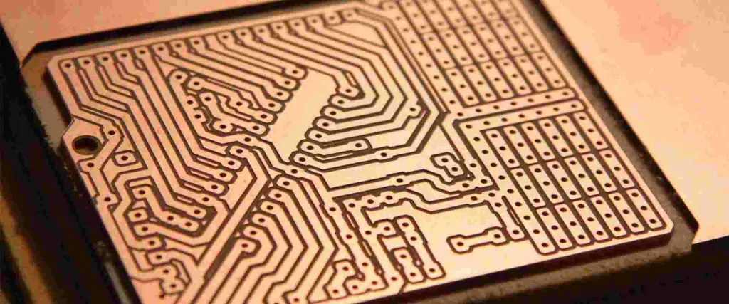
Printed circuit board etch-back is a technique used to maintain optimal transmitting signals between many layers in PCBs. It is specifically used with PTH procedures, where producers add a copper coating to the interior sides of the via. PTH enhances conductivity by linking the circuits in multilayer printed circuit boards.
Understanding PCB Etch Back Processes
PCB etch-back is a crucial process to maintain optimal routing signals between multiple layers within printed circuit boards. It involves removing the epoxy glue from the edges of the drilled via to allow electroplating and maintain the high link between layers. This process is especially important in high-reliability appliances. It is subject to standards set by an IPC-6013, which dictate that etch-back must expose a minimum of 0.003 mm and 0.08 mm of copper as specified in the Procurement records.
To improve the adhesion via plating, micro-etch procedures are used, which involve submerging the base laminate & drilling PTH into a multilayer printed circuit board. The dielectric debris and excess smears from a plated sidewall are then removeable using a plasma etch in the process known as de-smearing.
Moreover, PCB manufacturers utilize PCB etch-back in conjunction with de-smearing processes. PCB etch-back removes material from a via hole and extends copper layers to improve the electrical conductivity of the printed circuit board. This process allows producers to plate 3 edges of a copper layer & promotes the sustainability of the PCB design.
Two common processes in flexible circuit production, micro-etch & plasma etch, can impact etch-back. To enhance Coating adherence, the laminate substrate is often treated through a micro-scale etching, where a small copper is removed by submerging or spraying the substrate. After laminating the circuit layers together and drilling through holes, a plasma etch is performed to remove any organic resins or debris, also known as desmearing. It ensures the surface of copper in the via hole is lead-free. The plasma etching is carefully controlled to remove a specified amount of dielectric, revealing the copper coatings.
Causes of Epoxy Resin Smears
When the temperature of a drilling process surpasses the glass transition temperature of a substrate, it can melt the dielectric resin and its dispersion on the copper texture of interior layers, causing smears. This melted resin may obstruct the terminals of inner layers, leading to a decrease in the effectiveness of electrical connectivity.
Type of PCB Etch Back Processes
Two primary types of printed circuit board etch-back exist, namely negative & positive, and they yield various appearances & outcomes.
· Negative PCB Etchback
In negative printed circuit board etch-back, the inner copper coatings gradually recede from the walls of the via hole to varying degrees depending on the configuration of the PCB.
Negative etch-back is less aggressive and is more suitable for the production of high-durability & long-term installations.
Polished copper cylinder walls by negative etchbacks, which do not have stress points within the inner plane. But if we use these processes too much, it can cause gaps between layers because of dirt and air bubbles.
· Positive PCB Etchback
On the other hand, positive PCB etch-back results in copper pads sticking out from the intersecting edges of the via hole, which provides a sturdy Tri-terminal connection. This type of etch-back is commonly useful in highly reliable multilayer printed circuit boards, particularly in the aerospace, medical & military fields.
Positive etch-back is also useful to remove smears of dielectric substance aggressively. However, one significant disadvantage of this method is the potential formation of Pth barrels & foil cracks by strain accumulation on a fabric. Despite this drawback, positive etchback is still available.
PCB manufacturers have several options for etch-back techniques, each utilizing different solutions and yielding varied outcomes depending on environmental conditions. These options include chemical and plasma etch technologies.
· Chemical Etch
Chemical etch processes typically use a basic etching solution of potassium permanganate, usually removed via plating. Another option is sulfuric acid, which removes water from the air and has a limited period, changing resin-reducing rates based on purity.
Another chemical etch option is chromic acid. It gives a uniform resin removal rate but comes with water pollution hazards.
· Plasma Etch
Plasma etch-back is an expensive technique useful in PCB manufacturing that offers fast and effective stain removal. The process involves creating volatile radicals that corrode epoxy glue buildup, making gases that producers eliminate at the last step of the procedure. However, plasma etch-back can increase the total price of PCB production due to reduced manufacturing throughput and longer processing time. Additionally, after the plasma etch-back, you still require a chemical desmear procedure to get the glass to etch & remove any fiberglass.
Difference between Chemical & Plasma PCB Etch Back Processes
Etching is the process of removing copper & unprotected areas, leaving the intended board behind. There are two main methods of etching: chemical etching and plasma etching. Although both techniques serve the same purpose, they differ in several ways. The following are some of the differences between chemical etching and plasma etching.
· Efficiency
The most significant difference between chemical etching and plasma etching is their efficiency. Chemical etching, which removes unprotected areas by dissolving them, is effective, however inefficient, similar to digging a ditch. In contrast, plasma etching has set new standards by greatly improving efficiency.
· Etch-back
Another difference between chemical etching and plasma etching is the occurrence of etch-back. During the chemical etching procedure, etch-back or undercutting always occurs, which requires increased trace widths. The thickness of the copper also affects the etching time required to eliminate copper, which is present between the pads. On the other hand, the new procedure of plasma etching eliminates the occurrence of etch-back. Therefore, the occurrence of etch-back is another distinguishing factor between chemical etching and plasma etching.
· Etch factor
Plasma etching is crucial as it reduces imaging errors by utilizing an imaging process that transfers the layer to the substance/material, thereby eliminating an etching factor. But the chemical etching procedure is the traditional method that results in a distorted side of the pad. With chemical etching, there is a certain slope amount for every wire height increase.
Unlike chemical etching, plasma etching does not use a hot chemical solution like a manganate (VII) solution. It is a dry technique that is eco-friendly and has been proven effective in completely removing any leftover epoxy resin from the printed circuit board drilling process.
Compared to permanganate solutions, which rely on wet chemistry & chemicals that lose effectiveness over time, plasma ashing is a cleaner and more consistent process. It does not generate any hazardous liquid chemical waste. Additionally, the equipment needed takes up less area on the fabrication floor. Additionally, the plasma treatment tool is easy to operate and does not require highly-skilled personnel.
Wrap Up!
The terms “de-smearing” and “etch-back” may be used interchangeably by some manufacturers, but these two processes are slightly different. In particular, it is possible to perform de-smearing without requiring resin etchbacks.
De-smearing, or smear removal, removes resin from the via hole wall side to ensure proper interior layer electrical connectivity. Etchback, on the other hand, improves conductivity by extending or etching the copper layers. While some manufacturers may use the terms interchangeably, there are slight differences between the two processes. Etchback is more effective in multilayer printed circuit board configurations, while you cannot use it for PCBs with double sides.
Furthermore, chemical etch-back strategies are generally more cost-effective than plasma methods. Still, they are less efficient & involve caustic chemicals that may pose hazards during handling. On the other hand, plasma cleaning treatments offer greater precision, allowing for better customization and fine-tuning of the drilling process.
PCB manufacturers can opt for plasma processes as a safe & eco-friendly alternative to chemical etch-back methods. Plasma processes produce by-products that discard without gathering hazardous waste. By partnering with a specialized printed circuit board etch-back professional, manufacturers can achieve higher adaptability, optimized repeatability & precision for even the most complex fabrication processes. It leads to more reliable, more sustainable printed circuit boards, reduces waste & improves reliability. Although plasma etching eliminates the need for additional time to rebuild boards, resulting in low cost.
Boards must include via holes in order to establish electrical contacts between traces on different layers. But did you realize that vias might be useful to plug these holes?
Surprisingly, vias plugging refers to the common procedures used by the majority of PCB producers to safeguard PCB vias. What, though, is through plugging exactly? Continue reading to learn more about the limitations of filled holes or vias and the various methods for vias protection or plugging.
What Is PCB Via Plugging?
Manufacturers employ the method known as via plugging to fill holes or vias with solder masks or epoxy. Unlike via tenting, when makers fill the holes instead of covering them, this is the complete opposite.
Plugging in might be viewed as a safety precaution. During assembly or soldering, it stops additional solder substances from pouring into the soldered hole.
In simple words, disconnected vias provide spaces for unwelcome solder paste to flow, resulting in solder junctions. It’s interesting that manufacturers may plug vias with both conductive and non-conductive substances.
Also, the use of non-conductive substances to plug through holes won’t have an impact on how they work. The disadvantage is that they are not strong enough to withstand larger current loads.
On the contrary, vias that have been filled with conductive substances may easily transfer significant current loads between layers. There’s a grab, though. Conductive material-containing vias might have significant CTE.
Hence, there is a good likelihood that the conductive substance will heat up and expand more quickly than the laminate around it. However, such circumstances may lead to cracks between the contact pad and the wall.
When temperature or a significant quantity of current has to be transferred from one portion of a board to the other, conductive-filled vias are typically employed. They are located underneath chips where excessive heat is an issue. Also, there will be a great deal of heat being produced. The metallic quality of the filler will typically conduct heat like a heater in many aspects, from the microchip to another edge of the circuit.
The mismatch in CTE between the surrounding laminate and metallic fille is the fundamental disadvantage of conductive-filled holes or vias. Fractures or Cracks between the holes and pads wall may result from the metal’s fast expansion and heating relative to the laminate around it. Although the fill’s goal is to increase the integrity of the metal pad, plated on holes. Conductive filled holes or vias really aren’t advised for Via or through-hole In Pad process due to this.
· Non-conductive Fill
It’s a frequent fallacy that perhaps a non-conductive filled will allow just a very faint electrical signal to travel through a via if any, electrical signal at all. It is untrue. The only change is that the fill substance is used in place of the empty space in the barrel’s space of the vias. They may still be coated with copper like every other via holes on the circuit. This is often done to stop solder and other impurities from getting into the through. Or for a via-in pad to give structural strength to a metal pad surrounding the exposed hole. A mask-plugged hole or vias is also known as a non-conductive fill.
Plugged Via Shut With Copper
This refers to an early callout that is occasionally found on heritage goods. This was originally intended to be a means to create a copper conductive stuffed via as the copper utilized to print a via sealed will also print across all copper aspects on the circuit. The challenge with this procedure involves the fact that the vias must be very tiny to make this practical. All holes and copper on the surface.
As one copper oz is equal to 1.4 mils, it takes 2.8 oz of plating to cover an eight mil drilling hole. Because the plating is used on both “ends” of the hole barrels, 8mil/2 is equal to 4. 4mil/1.4 is equal to 2.85oz. This really is 2.85 oz more copper than what is currently on the board’s surface. This would increase the overall copper weight of the design to 3.5-4 oz. With this much copper, it is impossible to create intricate trace designs or tight spaces.
The enormous difficulty in coating the hole’s whole barrel equally is another disadvantage. A hole may seem sealed, but the middle may contain trapped air or fluids that will release when subjected to assembling temperatures since the hole barrel tends to plate quicker toward the holes’ bottom and top. We won’t try this kind of fill because there are far more dependable options available.
As previously noted, there are two ways to plug a visa. However, it varies depending on the substance (non-conductive or conductive materials). The non-conductive through plugging is much more common among these two. Now let’s examine these techniques in more detail.
Conductive Via Plugging
This plug-via method is perfect for PCBs made for applications requiring significant current transfers, often from one surface layer to the other. Moreover, conductive through plugging offers superior heat dissipation capabilities.
Pros
Conductive hole plugging offers heat sink or transmission in places where conventional means can’t, such as the base of a chip component.
Improved thermal conductivity results in a higher current-carrying capability. The conductivity of the substance might range from 3.5-15 W/mK.
Cons
The pad and copper plating within the via may become unstable as a result of this operation. The disparity in CTE values between the conductive substance and overlying laminate is the cause of this issue.
More expensive than its via-plugging equivalent that is non-conductive.
Not that many people request conductive plugging for cables.
Epoxy Resin Or Non-Conductive Via Plugged Via
This approach is more often used than conductive ones. Manufacturers stuff the through-hole, in this instance, with non-conductive substances. A number of variables, including design specifications, accessibility, plugging machine, and CTE value, affect the plugging substance.
Nonetheless, this technique typically has a thermal conductance of 0.25 W/mK. Even yet, the plugged hole won’t convey ineffective messages or useless cash. Furthermore, it is quite challenging to distinguish between vias connected with non-conductive substances and those on a typical PCB.
Pros
Plugging into a non-conductive via is more dependable and sturdy. These filters also have comparable CTE with laminate, unlike conducting compounds.
It prevents solder and some other impurities from entering.
In order to sustain active pads structurally, non-conductive through plugging is sturdy enough.
Cons
Due to its limited thermal conductivity, it might not be able to tolerate strong currents.
While placing your PCB request, you could be unsure about the distinctions between plugged and tenting vias. Nevertheless, the following paragraph clarifies them for you.
Tenting consists solely of covering the via holes and the circular ring with solder masks. It works especially well to avoid element exposure & lessen inadvertent shorting or contact. However, producers don’t take particular measures to guarantee that all the via holes stay closed, which reduces its functionality.
On the contrary, plugged vias include the filling process of the vias using ink. Because of this, manufacturers take special precautions to guarantee that all vias remain blocked and closed with masks. Moreover, plugging solutions do not address the aperture yellowing issue.
Via-in-pad differs from tenting and plugged vias. Drilling your vias into the footprint pad of BGA without any modification occurs during PCB manufacture. Plugged vias provide the best functioning out of the three.
Design Requirement
If the designs call for tenting files, you must provide fabrication comments. Either a readme.txt document or a design in Gerber fab can provide this information.
The Gerber fab seems to be more specific and expresses plans to take off various masks. Without this information, manufacturers can put your purchase on technical hold.
Also, if your design calls for plugged vias, you should inform your manufacturers. Similar to tenting, you may indicate it in the fabrication print or include it in a readme.txt document. You’ll also need information on the size, number, and placement of vias that you intend to plug in.
When submitting your fab notes to the manufacturer, it is essential to note the criteria for the via-in-pad.
Pros And Cons
The simplicity of a tenting procedure is one of its benefits. Manufacturers can finish the single-step procedure fast. Unfortunately, tenting does not ensure complete security.
In contrast, every plugged via is entirely filled and covered. Moreover, clogged vias could cost you more money and extra steps to accomplish.
Conclusion
Your vias must be completely protected, which calls for plugged vias. Because of their advantages despite their drawbacks, plugged vias continue to use often for soldering and assembly.
Moreover, producers have two materials at their disposal to fill PCB vias. While non-conductive materials are good for low-current devices, conductive materials are ideal for high-speed Boards. Last but not least, deliver the necessary Gerber files to avoid any problems with the producer.
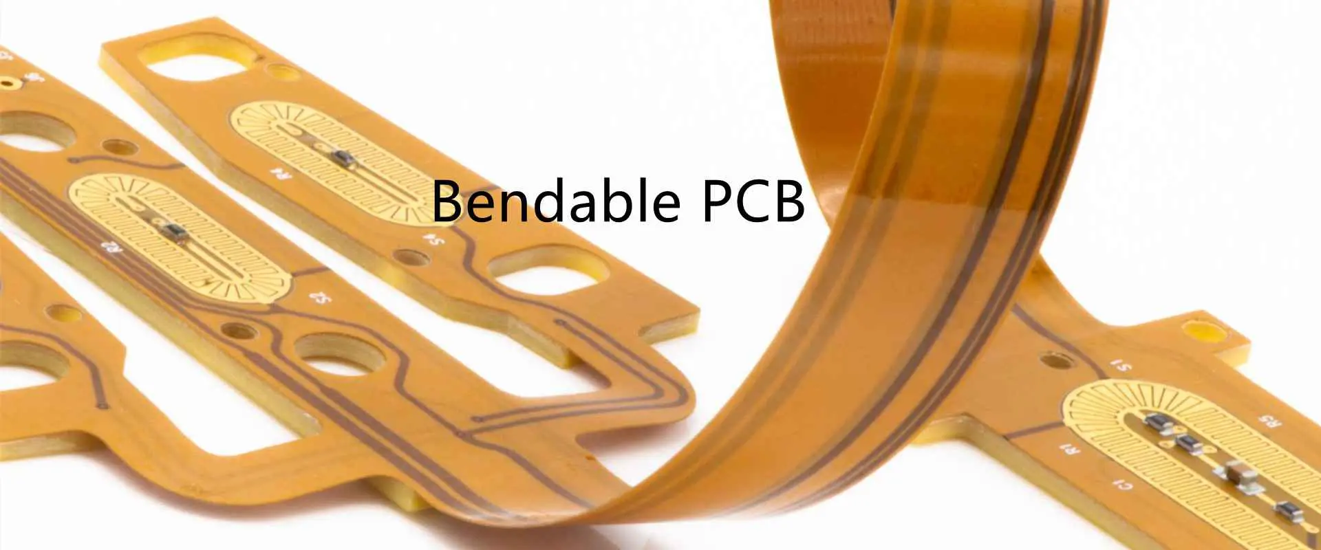
Flex-rigid PCBs offer a vast array of uses as a result of the trend toward downsizing in the creation of consumer devices. Also, the PCB sector has been experiencing fiercer competition, which has increased the focus on flex-rigid Circuit Board manufacturing technology development. Several PCB manufacturers who specialize in rigid Circuit board fabrication are unable to match the expectations of flexible Board fabrication due to the complicated process of flex-rigid Circuit board manufacturing. The type of PCB is FR4 semi-flexible Circuit Board which we will discuss in this article. It comprises bendability, flexibility, and the ability to construct in three dimensions.
It is impossible to exaggerate the significance of flex-rigid Circuit boards in PCB manufacture. The single driving factor behind it is the expanding trend of product miniaturization. Also, the need for flexible-rigid Circuit boards is increasing due to their flexibility and ability to construct in three dimensions. Not all Circuit Board producers can, however, accommodate the challenging flexi-rigid PCB production process. Semi-flexible PCBs create in a way that reduces a rigid board’s thickness to 0.25mm or 0.05mm. The board can easily employ applications that call for flexing the circuits and putting them within casings as a result. The Circuits can easily use for both single-bend installations and setups involving several bends.
The ability to adapt to the given area and be flexible are the most crucial qualities that make it suitable for numerous uses.
The reality is that flexibility doesn’t affect the transmission of signals, which enhances its widespread use.
Also, it is naturally lightweight.
Semi-flex Circuit boards are frequently renowned for their lowest possible prices due to the fact that their fabrication process is in line with present production capabilities.
Both throughout the design process and during assembly speed things up.
They are a very trustworthy choice, especially since they prevent several problems like welding and entangling.
PCB Fabrication Procedure of FR4 Semiflex
The following is the general process for creating FR4 Semi-Flexible PCBs. Generally speaking, the procedure involves the following elements:
Issues & Solutions In The FR4 Semiflex Fabrication Process
The main challenge in manufacturing is to maintain precision and milling tolerance for depth control. It’s crucial to check for resin fractures and oil peeling, both of which might result in quality problems. This means keeping an eye out for the following things while using depth-control milling:
Board Thickness
Resin Material
Milling Tolerance
Depth Controlling Milling Test A
For thicknesses of 0.3 mm, 0.275 mm, and 0.25 mm, the depth milling is carried out using the mapping approach. After this, the panel is tested to determine whether it can withstand the 90-degree bend. Generally, fiberglass is considered damaged if the remaining thickness is 0.283mm. So, when performing the depth milling, it is essential to take into account the panel thickness, the thickness of the fiberglass, and the dielectric condition.
Depth Controlling Milling Test B
Depending on the foregoing, it must be assured that the copper thickness between the L2 and solder mask range is 0.213mm and 0.188mm. Proper consideration must also be given to every warpage that could happen and affect the consistency of the overall thickness.
Depth controlling Milling Test C
When the panel has been prototyped, depth-controlled milling is crucial to guarantee that size is fixed at 6.3′′x10.5′′. Following that, the mapping point measurement is done to make sure the 20 mm horizontal and vertical spacing is maintained.
A unique manufacturing technique ensures that the deep-regulated thickness tolerance is within the limit of 20 m.
Composition Of A FR4 Semiflex Material
The purpose and final usage of an FPC often dictate its composition. The capacity of the material to sustain high electrical conductivity whilst resisting warping, breaking, and damage also plays a role in how flexible it is.
Because of this, manufacturers frequently create semi-flex PCBs by pouring a mixture of fiberglass and epoxy glue into fiberglass materials or FR-4.
But let’s look at some other components of a semi-flex PCB material.
1. Insulating Film
Polyethylene layers with high density are insulating films. These are created by forcing resin using a nozzle right before putting it on the FPC base.
Moreover, this HDPE coating prevents the substrate from being impacted by capacitive coupling. Electrically insulating connections on the upper layer also interfere with other circuits.
Moreover, an insulator film layer acts as a moisturizing barrier to shield the PCB from moisture as it cures.
2. Electrostatic Adhesion Layer
Well, after insulating the film, there is an adhesive layer to aid in holding electrical components on the board. This board layer is often acrylic or polyimide, allowing parts such as LEDs to connect directly to the flexible PCBs.
The electrostatic adhesive layer significantly reduces the amount of time and resources for assembly.
3. Conductor
Incorporating an electric conductive layer over the adhesion assists in avoiding circuit warping. Polyamide, epoxy resin, and the panel itself can also use as the coating.
Remember to spray the conductor with a 100C solvent to prevent warping effectively.
4. Board Enhancement
A second adhesive improves the FPC further. Also, it lessens the possibility of experiencing fracturing or bending issues. Manufacturers frequently use cellulose or acrylic to create the coating.
5. Coverlay
The last plate to shield the underside of the FPC material is the coverlay. Because it comprises acrylic or polyamide, the coverlay can also serve as an insulating layer.
It thus shields the FPC substance from dampness.
Moreover, the coverlay offers high-temperature tolerance, enabling the use of FPC boards in heater and oven applications.
The most typical sort of circuit board is a PCB, although even this form is not suitable for all purposes. FPCs, in contrast to PCBs, can flex and bend, making them ideal for contemporary technologies.
Also, relative to their conventional counterparts, Flexible PCBs provide greater heat dissipation, increasing the durability of the devices you create with them.
PCBs come in three different varieties: single-layered, double-layered, and multilayered versions. FPCs, whereas dividing into flat flex boards and semi-flexible boards.
Application Of FR4 Semiflex PCB
· Medical Imaging Instrument
Medical devices need a great deal of semi-flex Circuit Boards. Medi-care equipment, including endoscopes and imaging tools, employs a semi-flexible PCB. A flexible tube called an endoscope has a lens and a light at both ends. It is put inside the human body to observe internal organs or carry out treatments. These include tissue biopsies, draining fluid clumps, removing foreign objects, and widening congested channels like the esophagus. Low cost and superior electrical performance are two benefits of semi-flex PCB. The semi-flexible PCB is appropriate for this use since it can be twisted into the correct form.
Further uses for semi-flexible PCB exist in the medical industry. For instance:
Circuit board for protecting injection needle tips (ETC)
PCB for temperature control in medical equipment
Circuits for a mobilized blood pressure monitor
· Automotive Applications
Automotive devices with vibrations and high temperatures employ semi-flexible PCBs. The flexible architecture guarantees that the PCBs won’t crack from vibration or mechanical shock when operating at high temperatures. To suit the needs of the majority of applications, they are manufactured from stiff FR-4 fiberglass epoxy composites with extra copper layers bonded on each side of the substrate.
Due to their inherent flexibility, Semi-Flex PCBs are perfect for serving automotive applications with high-temperature requirements, such as Digital Control Systems or DCU, Electronic Control Units or ECM, etc. These boards are resistant to breakage and distortion at high temperatures of 150 °C.
· Aeronautics
With the rising demand for weight reduction and miniaturization, the usage of rigid-flex circuits for aerospace devices has expanded. As interconnect modules, rigid-flex Circuits are an efficient way to decrease size, weight, and energy consumption while enhancing dependability.
Several aircraft applications, including avionics, communications, and military systems, have employed rigid flex Circuits. Rigid-flex PCBs are useful in aviation applications as connectors between PCBs and additional parts like switches, displays, or cables. They aid in reducing the number of connections needed on Circuits, which aids in reducing system weight. They also improve dependability by cutting down on the number of linked components.
· Wearable Devices
The most well-known examples of wearable technology are fitness trackers and smartwatches, which are gaining popularity. Small, battery-operated gadgets that one wears over the body are wearables. In wearable technology, rigid-flex circuits and semi-flex circuits are both employable, with rigid-flex circuits being more popular in watches & semi-flex in fitness trackers. This is due to the fact that semi-flexible materials are more suited for wearables that must bend on the body. At the same time, stiff flex can sustain bending pressures, which is vital for wearables that require to endure impacts while falling.
PCBs that can flex and not bend are frequently useful in applications that need semi-flexible Circuits. For instance, semi-flexible boards are frequently useful in high-end tablet and smartphone systems. With these gadgets, the back of the screen is directed to a very thin layer of a semi-flex board. This enables the display to bend or fold without breaking. When only a little amount of flexibility is required, a semi-flexible Circuit can easily be employed. These may use, for instance, on the back of a gadget with a stiff front panel, like many computers and tablets.
· Gaming Devices
The primary benefit of adopting rigid flex Circuit in game consoles is that it offers superior protection against physical shock damage. They are better able to endure powerful external pressures like collisions and drops due to having lesser layers than conventional rigid PCBs. When compared to a conventional rigid PCB, the layers of rigid-flex Circuits are more resilient to bending. Therefore, if you somehow drop the gadget, it will sustain the greater force. For instance, the stiff flex PCB may readily twist or bend without cracking or breaking while using a gaming system, which frequently demands bending.
Conclusion
Due to certain of its characteristics and qualities, rigid or semi-flex PCBs will perform better than their competitors in a number of areas. They compete fiercely with other PCBs on the market since they perform comparable tasks and give end consumers a more affordable choice. Some of these uses are with one another, while others do not fit well into any one category. Whatever one you choose to develop will depend on your own demands and preferences.
Numerous printed circuit board layout & routing guidelines used presently aim to ensure signal integrity, even for speed signals & devices. For individuals new to printed circuit board design who have not encountered any signal integrity issues, the idea of guaranteeing signal quality in a layout may appear abstract. However, straightforward layout practices can help solve or prevent numerous problems that modern PCBs may encounter. The main objective of signal quality practices is to detect and rectify issues in a printed circuit board design. It ensures that digital/analog signals remain uncorrupted during transmission through interconnects and can be retrieved at the receiving end without degradation.
This guide aims to summarize signal integrity issues that may arise in the printed circuit board layout, along with fundamental remedies to address them. By incorporating these foundational techniques during the initial design stage, maintaining signal integrity throughout the routing process becomes more straightforward.
At its core, the objective of applying signal integrity practices in printed circuit board layout & routing is to guarantee that the signal remains uncompromised as it travels from its source to its destination. In simple terms, the objective is to guarantee that the signal obtained at the ending point of the interconnect is a precise depiction of the signal initially transmitted at the beginning. Although a signal can never be completely free of distortion, following some fundamental practices can reduce signal distortion to a minimum and ensure that the receiving component always detects the accurate signal.
Implementing specific design practices can guarantee this outcome, starting from the schematic capture & film stack design phase. Proper stack-up design & finish assignment for ground, power, and routing can resolve numerous signal integrity, power integrity, and EMI/EMC issues. Additional uncomplicated methods consist of selecting the appropriate capacitor, computing impedance, and comprehending the constraints of single-conductor and differential traces.
When Should One Think About Signal Integrity?
Every design has signal integrity issues, but they typically do not impact a product’s functionality or generate excessive noise unless working with speedy digital signals/high-frequency designs. When dealing with these types of designs, there are several issues to consider.
To avoid signal reflections, precise impedance calculations are crucial.
Long can experience losses & dispersion during Fast switching signals can cause crosstalk.
Extra radiation losses can manifest as significant noise in Electromagnetic compatibility tests.
Regarding digital signals, issues like overshoot undershoot, and ground bounce can arise from excess inductance.
Parasitics can lead to high-frequency signals becoming coupled and potentially degraded.
Fiber weaves can cause skew and resonant frequency loss, negatively affecting signal timing and integrity.
Jitter can occur in digital signals due to either random fluctuations or SI/PI/EMI issues.
The copper surface texture along the distance of an interconnect can cause additional losses.
Signal integrity can be a challenging issue to tackle when dealing with high frequencies or fast switching speeds commonly found in speedy digital boards. Nonetheless, one should implement certain straightforward design measures to safeguard against these problems and prevent design failures.
To ensure signal integrity, it’s essential to establish a well-defined ground & keep it near vital traces during the routing process. You can achieve it by implementing a well-planned stack up, carefully selecting ground & power planes, and appropriately assigning signal layers. By taking these steps, most electromagnetic interference (EMI) and signal quality issues can be effectively addressed. Additionally, a properly designed stack-up can have a positive impact on power quality as well.
The stack-up diagram below illustrates a common configuration that employs alternating layers of signal, power, and ground. In this case, the design incorporates ground layers near the analog layers to achieve shielding, establish a ground plane, and facilitate the definition of impedance lines (such as strip lines/microstrips). To prevent reflections, minimize radiation & reception of electromagnetic interference, and shield against signals on different layers, it is beneficial to establish a low-impedance return path with well-defined trace impedance and ground near signals.
The impact of layer thickness on losses in digital/analog signals transmitted through stripe lines, microstrips, and coplanar arrangements is a widely recognized phenomenon. One way to mitigate losses is by carefully selecting the dielectric thickness for signal coatings that carry high-speed or high-frequency signals. By selecting appropriate materials & plating for traces, it is possible to achieve reduced losses at very high frequencies, particularly in mmWave layouts that demand accurate signal integrity. Implementing these measures collectively can guarantee minimal signal losses during transmission through an interconnect to its final destination.
Significance of Impedance & Routing for Signal Integrity
After finalizing the stack up and placing crucial components, the layout process entails tracing the routes. Impedance requirements, as specified by signaling standards employed in user interfaces & high-frequency signals, must be adhered to to ensure the quality of signals & prevent complications in speedy channels. While routing, particular attention must be given to key geometric characteristics of tracks on the printed circuit boards.
To achieve optimal impedance, single-ended & differential signals must be considered.
Maintaining a tight path throughout the signal route is crucial and can be achieved by using uniform planes & grounded vias.
Decreasing via transitions & excessive bends is important, especially at frequencies of 10 GHz and above.
Via stubs should be removed from the fastest and highest frequency signal routes.
The initial two points aim to guarantee that the capacitance along a pathway adheres to the prescribed design value outlined in the applicable signaling protocol. The 3rd point pertains to minimizing EMI & noise interference by ensuring that the signal current formulated by high-speed or high-speed signals has minimal inductance. The last two points focus on eliminating loss & echo at any point of impedance variation along a pathway.
Components such as vias and connectors may have an input capacitance that diverges from the desired value. Design rules are implemented to ensure these specifications are met during the design process.
Your printed circuit board design software’s routing tools can convert your routing specifications into layout rules to ensure that you meet your goals for impedance via count, spacing & return path. Backdrilling incurs a price tradeoff that affects signal integrity; therefore, it should be applied only to fast digital signals and as a last resort if there are no other routing options available to reduce the requirement of back drilling.
Together, these steps can effectively tackle issues that may result from reflections, including intersymbol interference within an eye pattern and standing waves on transmission lines that are not properly matched.
Detection of signal integrity issues requires either simulations/measurements. It is preferable to perform simulations during the design phase to detect and address potential signal integrity issues before prototyping. An effective approach is to make test circuit boards for the layout, enabling measurements to be taken before moving into high-volume production. Regardless of the chosen approach, identifying signal quality issues should be finished before scaling the layout for high-volume creation.
Simulations During Routing
In the layout phase, certain ECAD packages can detect signal integrity issues through simple simulations. Crosstalk waveform calculations & ringing are two common emulations that could be simultaneously executed. The information can typically be specified in datasheets. By running these simulations, one can understand the impact of terminations & interconnect spacing on the transient response of the interconnects.
There are additional points to verify while routing, such as:
Undershoot and Overshoot
Fall time or Rise time during switching
Skew present in both differential pairs and parallel buses
ground continuity
You can use advanced ECAD software packages with online simulation tools to verify these points during the PCB design process. After routing the design, an electronic design automation (EDA) tool can assess these points. It ensures that the signals on every interconnect stay within sound margins. It also exhibits the necessary response as perceived at the receptor component.
Detecting these issues in the initial stages of the layout process can help resolve numerous signal quality problems, potentially eliminating the need for complicated & time-taking redesigns.
Possible Problems Due to Weak Signal Integrity
The impact of obstruction on the functioning of electric appliances can be quite significant. In the past, flight attendants would advise passengers to turn off their cell phones. We would encounter radios that created static audio. Additionally, certain older computers emitted so much Electromagnetic interference that they were removed from the market. Signal integrity issues typically manifest in more subtle ways than obvious performance degradation. Examples include intermittent data loss, occasional glitches, or even complete device failure in extreme situations. These problems are often rooted in signal integrity issues.
With the rise in signal speeds of modern electronics, they become increasingly vulnerable to aggressive interferences, such as impedance mismatch-induced signal reflections, ground bounce & crosstalk.
Without appropriate countermeasures in the printed circuit board layout, these issues can cause signal degradation. Then, it ultimately renders the system inoperable. Apart from avoiding signal integrity issues in external components, it is equally important to ensure that the printed circuit board does not contribute to signal quality issues for its circuit or other electronics. Therefore, before delving into the specifics of designing for such problems, it is essential to have a solid grasp of the critical signal quality fundamentals.
Various factors can contribute to signal degradation on a printed circuit board, which can be classified. Below are four key areas of inadequate signal quality that require attention.
· Electromagnetic Interference (EMI)
Improper routing of high-speed signals on a circuit board can result in the emission of electromagnetic interference (EMI). It’s not just the length and arrangement of the traces that can cause issues, but also the trace & via stubs that act as the antenna and contribute to the problem. EMI can also arise from the signal path. It should ideally be on the adjacent ground plane to minimize its effects. Any obstruction in the ground path can cause the signal to emit even more sound as it tries to find its way back to the source.
When high-frequency traces are placed too close, they can unintentionally interfere, causing one signal to overpower another. This interference, known as crosstalk, can cause the affected signal to imitate the properties of the disruptive signal and fail to carry out its intended function. Crosstalk is not only a concern for footprints that are located adjacent to the same layer. But also for traces that run parallel to each other on side-by-side layers of a circuit board, this form of crosstalk is transverse coupling. That’s why many circuit board layouts adopt alternating vertical and horizontal directions on side-by-side layers to mitigate this issue.
· Simultaneous Switching Noise (Ground Bounce)
On a printed circuit board, when numerous components switch between low and high states. The current level may not return entirely to the ground potential during the falling edge if the voltage level during the falling edge transition rises excessively. The low-level signal is identifiable as the high-level. When this phenomenon happens concurrently, it can result in double or false switching, leading to circuit operation disruptions.
· Impedance Mismatch
When the consistency of high-frequency transmission lines is alterable, it may cause signal echo that compromises its integrity. Traces routed without proper consideration for their capacitance value are prone to changes in value in different areas of the board under varying conditions. To ensure the appropriate routing of impedance-controlled traces, a trace width, certain layer configuration & clearance are necessary.
Now that we have identified the primary signal integrity issues, let’s examine some printed circuit board design procedures that can mitigate these problems.
PCB Layer Configurations and Component Placement
Signal integrity issues in PCBs commonly arise from inadequate signal ground paths. To ensure optimal signal integrity, the ground path must be unobstructed and located on a close reference layer. To make it work, you need to arrange the layers in the board in a specific way that separates the sensitive high-speed routes and keeps them close to reference planes. This arrangement can be either in a microstrip or stripline style. In a microstrip setup, the traces are located on the surface and have only one underlying plane. In contrast, in a stripline setup, the traces are available internally and are sandwiched between 2 reference planes.
It’s good to have a reference plane next to signals so they can travel back smoothly. However, it becomes even more critical for delicate signals that require controlled impedance routing.
To figure out how wide a path should be for this kind of routing, you have to calculate the width & strength of the material around it, as well as the thickness of the path itself. Before starting the layout process, designers need to decide how they want the circuit to look because changing the board layers or substances used for making the PCB can affect their plans.
After determining the circuit stack-up layer configuration, the next stage involves placing the elements on the circuit. High-frequency circuits often contain multiple nets that originate from the source of one component, traverse via other parts, and terminate at a load sensor of the last component. You should maintain the signal paths in a circuit to preserve their signal quality.
It requires placing the components in sequence as indicated in the blueprint, allowing for the short link between pins. Space the other elements, like processors & memory chips. It helps to accommodate their routing techniques while also being close to short links. Here are the additional essential considerations to remember during component placement.
· To ensure proper placement of high-frequency circuitry, it’s important to follow these guidelines:
Situate bypass capacitors near the power connectors of processor & memory applications.
Allocate sufficient space for both bus routing & escape routing.
Also, Follow the assembler’s layout for DFM guidelines.
Guarantee that hot-running elements are properly cool down
With the parts on the board, the next step is routing.
Once you reach this stage, you’ll commence trace routing. However, it’s important to remember that the quality of signal integrity is highly dependent on the placement of the components. For instance, you should meticulously plan the escape routing to guarantee that all the signals are accompanying components. Many designs rely on via-in-pad for large pin-count BGAs to keep connections short and open up more room for routing.
When you position the components optimally, you can route high-frequency circuitry effectively. Nevertheless, there are some guidelines to bear in mind before you proceed:
Ensure that signal traces are direct and short.
Whenever feasible, route sensitive signals on inner layers & alongside or between standard planes.
It is important to keep clock lines & other high-frequency signals isolated from other places. A useful guideline to follow is to maintain a spacing that is three times the width of the trace being useful.
Ensure that differential pairs are together and avoid separating the couple around obstructions.
If you connect a bunch of wires that need to be the same length, begin with the long and then make the other wires go the same length by adding curves where needed.
Don’t put important wires through places on the circuit board where there is a lot of electrical noise, like where the power goes or the analog signals are.
If necessary, provide enough space for certain routing topologies like daisy chains.
To prevent additional signal integrity issues, limit using through-holes and minimize their inductance and length.
Apart from routing, it is essential to make the power PDN for the board. A clear PDN is essential for maintaining power integrity and promoting good signal quality. Moreover, it’s crucial to avoid routing high-frequency transmission lines via blocked areas on a standard plane.
Routing high-speed transmission lines through blocked areas on the reference plane can result in increased electromagnetic interference (EMI) generated by the board.
To ensure good impedance control, it is important to balance size, cost & signal integrity when choosing the number, type, and arrangement of the PCB layers. A general guideline is to incorporate power & ground planes. To ensure optimal signal path continuity, we recommend distributing the planes in the stack up evenly. Ideally, at least one plane should be adjacent to each signal layer without any breakpoints. Additionally, one can carefully evaluate the material properties, such as copper thickness, dielectric thickness, and dielectric constant, as they play a significant role in signal performance.
When it comes to circuits with fast signal transmission, traditional materials like FR-4 may not be the optimal choice. Instead, we recommend opting for laminates with less Dk, as they can minimize distortions & phase variations in the signal. Rogers laminates, like Rogers RO4350, are excellent examples of such materials. Although they may come with a higher price tag, they offer certain properties tailored to high frequencies surpassing FR-4.
· Impedance control
Impedance control involves determining the optimal relationship between the positioning and size of PCB traces and the characteristics of the foundation to ensure that the signal intensity remains within predefined boundaries. Effective coupling achieves a strong signal, while poor coupling results in power losses & compromises signal integrity.
To achieve effective impedance coupling, the PCB traces need to have consistent geometry, which ensures a uniform Dk along the whole trace. To verify the impedance (capacitance) value, designers can adjust the width of tracks & utilize specialized calculators that are readily accessible online. Neglecting this aspect can lead to signal reflections, where the signal reflects its origin point. It reduces signal strength reaching its destination, and there is an increased risk of EMI. It results in reducing signal strength reaching its destination.
Signal Integrity in PCB Manufacturing
The integrity of a signal is closely related to the routing of high-frequency transmission lines, and effective routing techniques begin with the careful placement of components. Initially, identify the functional areas of the board,. One can place components in a way that offers the shortest & direct signal tracks for high-frequency circuits. However, before commencing with component placement, it is essential to create a board stack-up that will optimize the impedance traces for the layout.
It is a common desire to avoid buying an electronic device only to experience its malfunction just after a week of usage. We have been using the same LCD monitor for more than five years now. We can confidently say that it is one of the most resilient electronic equipment we have ever possessed. If you value dependable products, you are likely to take note of industry standards aimed at enhancing the lifespan of electronic devices.
The reliability of Through-hole plating in the printed circuit board is essential. It ensures the plating can endure shock & thermal cycling. That’s why plating processes play a vital role. The latest plating standards in IPC 6012E mandate the use of strategies that enhance the dependability of VIP structures.
To establish signal connections between films in the multilayer printed circuit board, via holes in filled via-in-pad structures must undergo copper plating. This plating enables connections to other Contact points within VIP structures and directly to a trace via a small copper ring. Although indispensable, these structures are prone to reliability issues during thermal cycling.
In compliance with IPC 6012E, via-in-pad structures must undergo copper cover plating. It entails filling the copper plating around the perimeter of the through-hole & extending it onto the annular ring encircling the via pad. This mandatory procedure enhances the durability of the through-hole plating. It may minimize failure resulting from cracks or the detachment of surface features from the plated through-hole.
There are two types of filled copper cover structures. The first type involves the application of a copper film to the interior of a through-hole. It then covers the bottom and top films at the via ends. This wrapping of copper plating serves as the through-pad & trace that leads to the through-hole, creating a copper structure.
On the other hand, the through-hole is equipable with a distinct pad layer that forms around its ends. It connects to either traces/ground planes. In this case, the copper coating that fills the through-hole covers the upper part of the outer pad. It results in a butt joint between the via pad & copper plating. Although there is some bonding between the via pad & fill plating. The 2 don’t merge or create a unified, continuous structure.
Reliability of Copper Wrap Plating Under Thermal Cycling
During the thermal cycling of a PCB, the copper cover plating, fill material, and laminate interfaces experience tensile stress. It is due to volumetric expansion. Various factors, such as the temperature gradient between the board determine the magnitude of this stress.
When the thermal expansion coefficients of board materials do not match, it can result in notable stress on the copper cover plating. It leads to cracks & separation in the through-hole barrel and butt joint. At the end of the via, the continuous copper cover plating may also experience cracking at the correct angle.
When the Internal of the through-hole detaches from the square joint, it results in a circuit failure. With continuous thermal cycling, you can expect more failures to occur as the board flexes. Vias that terminate near the outermost layer of the circuit board are at a higher risk of fracturing under temperature cycling because these layers tend to experience more significant flexing.
Although there is a risk of failure in the structures, copper cover plating remains more dependable than vias without it. The additional layer of covered copper reinforces the structural integrity of plating in a through-hole wall. It enhances the contact point between the through-hole plating & annular ring.
To enhance structural integrity, manufacturers may add cap plating over wrap plating. This process involves applying plating on the top & bottom sides of the through-hole, similar to the wrap plating. After stripping the plating opposition, load the through-hole with epoxy, and planarize the finish to create a smooth finish. This approach is the most effective way to optimize reliability while satisfying the IPC-A-600 Acceptability of Printed Boards.
It is feasible to apply IPC 6012E plating to buried vias. It provided that the buried through-holes are divided into some layer stacks. So the inner film stacks are plated using copper wrap plating, similar to vias. Each stack can be plated, and a prepreg can be utilized to organize the last stack up. Vias located on interior layers are plated just like vias.
Multilayer PCBs and Copper Wrap Plating
Multilayer PCBs play a critical role in the design of electronic systems. It ows to their numerous advantages such as being lightweight, offering high assembly density & compact size. By consolidating multiple PCBs onto a single board, multilayer PCBs can meet the stringent weight & space requirements of contemporary product development.
The construction of multilayer printed circuit boards involves a crucial element known as the through-hole structure. It connects the pads, traces & polygons across various films of the printed circuit board. The use of copper cover plating is a significant aspect of via construction in multilayer printed circuit boards, as it enhances the dependability of VIP. The focus of this article is to delve into multilayer printed circuit boards via(through-hole) structures & copper cover plating.
Via Structures & Copper Wrap Plating in Multilayer PCBs
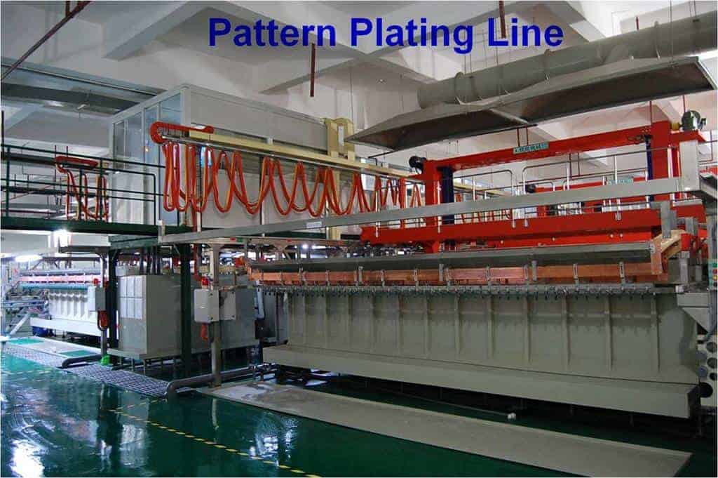
PCB pattern plating line
Copper cylinders, or vias, are inserted or created in drilled holes on a printed circuit board (PCB). Vias act as connections that unite pads, traces & polygons on various coatings of the multilayer printed circuit boards, serving both electrical and thermal purposes. Particularly in multilayer printed circuit boards, vias are essential in achieving a desirable component density. Including vias facilitates the interconnection of traces & components between different layers of a multilayer PCB. These structures enable the transfer of both power & signals across the layers. Additionally, incorporating vias simplifies the routing procedure.
Types of Copper Wrap Plating or Via Structures
The various kinds of vias present in multilayer circuit boards are classified as:
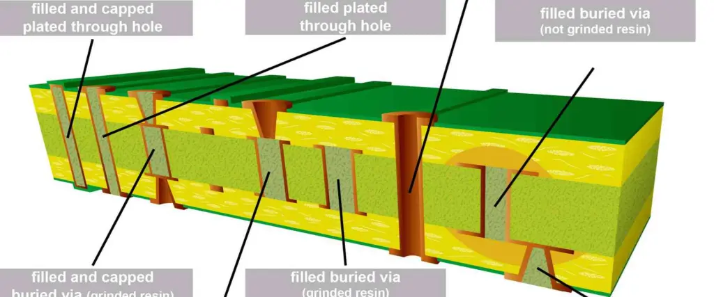
Through-hole via – The function of these vias is to establish a connection between the outer layers of the board by running through its entirety. If this via is coated with a conductive substance like copper, it transforms into a plated via, whereas if left uncoated, it is referred to as the non-plated via.
Blind via – Blind vias are the connections between an outer layer and an inner layer.
Buried via – Vias that establish connections exclusively between the interior coatings, without extending to the exterior coatings, are known as buried vias.
Regardless of the type of via structure, copper plating is essential to create a dependable via.
Copper Wrap Plating
In circuit board manufacturing, copper is important. It is extensively available on the layer planes of PCB and over the sides of via. Depending on the type of via, the placement of copper may vary. Through-holes have copper on the surface layer, while vias has copper in form of pating.
Copper cover plating is a type of electrolytic plating that extends from the plated through-hole structure to a finish of a printed circuit board. During the circuit board fabrication process, copper is inside the drilled through-holes, covering the copper annular ring on both the top & bottom surfaces. This plating process is continuous and envelops the shoulders of the plated via, providing an electrical connection between the top & bottom layers of the PCB.
IPC standards, including IPC 6012B & 6012E, define the copper cover plating & plating thickness requirements for all loaded plated vias. These standards categorize electronic designs into three classes: class one for general products, class two for dedicated electronic products & class three for high-reliability products.
To ensure a smooth fabrication & manufacturing process for your circuit board, it’s important to have the necessary software to communicate your board & parts information precisely. The last thing you want is for your design process by the need to search for the new supplier who can meet your specific requirements.
By utilizing an effective bill of materials, you can provide your partners & vendors with concise part instructions. In addition, coupling your design software with output files & materials bills can streamline the fabrication process, ensuring precision and ease of production
Altium Designer, exceptional printed circuit board design software, simplifies the process of defining your coating stack up, plating & designing the vias for your multilayer printed circuit board. With its top-notch capabilities, Altium Designer assists in designing devices that comply with the standards of IPC.
Numerous materials and laminates find utility in computing & industrial domains, particularly in constructing PCBs. The lamination bonding process involves layering several materials to create a waterproof and durable barrier, which helps shield and fortify various components.
The internal layers of the PCB are subjected to high levels of temperature & pressure during a gradual curing, releasing, and cooling process to make multi-layered printed circuit boards. One of the most robust and efficient laminates used in numerous PCBs is the Megtron 6 printed circuit boards for those considering whether or not to use Megtron 6 printed circuit board material, read on to discover the advantages and how it can enhance your products.
There exists a diverse range of laminates & materials suitable for industrial & computing applications, including the construction of PCBs. The bonding lamination procedure involves layering multiple materials to waterproof, reinforce, and safeguard various substances. To produce multi-layered PCBs, the internal layers undergo a gradual curing, releasing, and cooling process while subjected to high temperature and pressure.
Megatron 6 laminate is a durable and highly efficient material frequently utilized in printed circuit boards. If you are considering utilizing Megtron 6 in your products, read on to discover its distinct advantages and how it can increase your products.
You can choose three primary kinds of Panasonic printed circuit board laminates for your applications. The following are three options to consider.
1. Megtron 4 Laminate
Megtron, a Panasonic laminate, is suitable for low DK and high-temperature superconducting applications. It’s the most effective option among Panasonic laminates for network tools such as routers and antennae.
2. Panasonic Megtron 6 Laminate
For high-frequency and high-speed PCB applications, Megtron 6 laminates from Panasonic are recommended. Despite functioning similarly to PTFE laminate substances, Megtron 6 offers improved processability & speed.
Among other applications, such as telecommunication, computing & switching tools, this laminate is considered the best choice.
3. Megtron 7 Material
Consider using Megtron 7 substrate for your next multilayer PCBs with extremely low transmission loss. This advanced material offers the Lowest signal distortion available, making it ideal for high-capacity and high-speed transmission levels. Megtron 7 into your PCBs will significantly enhance their signal performance and strength.
What Is Panasonic Megtron 6?
Megtron 6 has gained popularity as a high-speed substrate material in various printed circuit board fabrication & manufacturing applications. This state-of-the-art basic substance is specifically engineered for a diverse range of high-speed measuring instruments, IC testers & mainframes. With its low signal distortion, thick layer, and multiple layers, Megtron 6 significantly enhances the performance of high-speed equipment.
Megtron 6 substrates possess exceptional electronic properties comparable to those of PTFE materials. It is due to high processability & distinctive advantages. By incorporating Megtron 6 laminates into your systems, you can significantly improve their performance across various fields, such as computing, telecommunications, & router applications.
Megtron 6 high-speed laminate sheets possess desirable properties, including a low dielectric constant, excellent thermal resolution, HDI capabilities, and improved stability. Furthermore, they are compatible with environmentally friendly soldering processes and can effectively prevent signal echoes at very high frequencies by using low-height foils for RF circuit boards. Megtron 6 substrates are produced using both conducting substances, mainly copper & insulating materials, typically made of fiberglass epoxy.
Besides, with this understanding of its manufacturing process, we can now examine the primary characteristics that differentiate Megtron 6 from other laminates within the Panasonic Megtron product line.
· Low Dielectric Dissipation of Panasonic Megtron 6
The degree to which a substance can function as an effective insulator or retain energy is reflected in its low dielectric dissipation factors (Df). Megtron 6 substrates are an excellent example, as they possess extremely low Df values, indicating high insulation efficiency. With a Df value of 0.002, Megtron 6 substrates offer exceptional performance, minimizing electric current leakage during operation.
· Low Dielectric Constants of Panasonic Megtron 6
Megtron 6 substrates possess excellent properties that enhance electrical conductivity, making them particularly suitable for power & high-frequency appliances that require low Dk to reduce electric power/energy loss.
Besides, with a Dk value of 3.7, these laminates exhibit minimal current storage, making them an ideal choice for such appliances.
· Low Transmission Loss
To meet the demands of modern PCBs, materials with low signal distortion are often necessary to minimize dielectric & conductor losses. Fortunately, Megtron 6 substrates exhibit low signal distortion and are well-suited for such applications.
· High Resistance to Heat
Thanks to their excellent dissipation features, Megtron 6 substrates can withstand high temperatures. It makes them a reliable choice in high-temperature conditions, as they won’t create a hazardous environment or cause damage to the surfaces they’re used on.
· Compliance Requirements
Megtron 6 substrates conform to both quality standards & environmental regulations established by the RoHS. This directive limits certain hazardous substances that can be present in electronic & electrical equipment. To ensure compliance with RoHS, any product or material must undergo testing to verify that prohibited substances fall within the prescribed limits.
The use of these laminates is suitable for lead-free appliances, which can help to restrict environmental pollution, ensure PCB compliance, and minimize exposure to prohibited chemicals.
Here is a more detailed examination of the various applications that Megtron 6 substrates are well-suited for and how they can be effectively utilized.
Regarding high-frequency equipment, selecting Megtron 6 substrates is the optimal choice. These laminates consistently provide the most precise results.
Megtron 6substrates are a suitable option for high-speed network equipment. They enhance the performance of communication devices utilized in interconnect routing and area networks.
Megtron 6 substrates can benefit high-frequency computer systems that process significant data. These laminates promote efficiency by ensuring the system remains in optimal conditions, contributing to overall system maintenance.
Megtron 6 substrates possess mechanical properties that enable IC testers to deliver highly efficient and accurate results when testing various integrated circuits.
Benefits Of Panasonic Megtron 6 Laminates
Megtron 6 substrates are highly efficient and offer numerous advantages for various applications. Below are the key benefits of utilizing Megtron 6 substrates.
· Through Hole Reliability
Megtron 6 substrates exhibit exceptional through-hole durability and robustness, rendering them suitable for multiple specialized appliances. Through-hole elements can withstand the greater environmental strain, such as elevated temperatures, and produce sturdier interconnections between layers. This technology is particularly advantageous for prototyping & testing that necessitates components, such as connectors, to endure mechanical stress.
· High-Efficiency Rates
By utilizing Megtron 6 substrates, you can attain more precise outcomes while upholding the performance criteria for high-frequency appliances. These laminates enable you to operate with greater efficiency, experiencing less disruption from both environmental and operational factors.
· Highly Durable
Besides their efficiency and reliability, Megtron 6 substrates are also exceptionally sturdy. Their robustness enables the substance to endure and retain its usefulness for extended periods, enabling you to maximize its utility. Moreover, their durability can withstand physical, mechanical, and chemical stresses, instilling confidence in you to rely on them for crucial projects.
· High Thermal and Electric Conductivity
Megtron 6 substrates possess exceptional insulation properties that optimize the electrical current flow and minimize leakage in both thermal & electric applications. Additionally, these laminates promote superior conduction of heat & electric currents, resulting in increased efficiency and productivity.
Understanding the characteristics of this printed circuit board material is crucial as it provides valuable insights into its functionality and performance.
· High decomposition temperature
With a 410°C decomposition temperature value, this material exhibits high resistance to chemical decomposition under high temperatures, allowing it to maintain excellent performance. However, exposure to temperatures exceeding 410°C can trigger its chemical decomposition.
· Low dielectric constant
The DK of this substance is exceptionally low, with the MEGTRON6 R-5775 circuit board material exhibiting a dielectric constant of 3.71 at a frequency of 1 GHz and 3.61 at 10 GHz. Furthermore, its Dk remains stable across various frequencies and temperatures, making it an ideal choice for high-frequency transmission applications.
· High glass transition temperature
MEGTRON6 R-5775 circuit board material boasts a 185°C transition temperature, signifying its classification as a high glass transition temperature material. Its outstanding performance is particularly evident in applications with various temperatures.
· Low dissipation factor
MEGTRON6 R-5775 circuit board material exhibits exceptional stability and an extremely low dissipation factor. At 1 GHz and 10 GHz, it records a Df value of 0.002 and 0.004, respectively. The dissipation factor, a property that measures electrical loss during discharge in the insulator, is an essential consideration when choosing insulating materials. With its low Df value, this PCB material minimizes electrical signal loss, improving efficiency.
· High peel strength
MEGTRON6 R-5775 circuit board material exhibits a robust 0.8 kN/m tensile strength measured by IPC-TM-650 2.4.8, indicating its exceptional bonding properties.
Storing the Panasonic Laminates
Given that there are various kinds of Panasonic circuit board material used in printed circuit board production, it is crucial to understand the appropriate storage conditions to maintain the quality of the boards. The following are the primary storage guidelines for Panasonic substrates that must be observed.
To prevent bending & scratching, ensure that the laminate remains flat and store it in a dry, cool environment.
Preserve the actual/real container given by the producer to store the Panasonic substrate.
Store the laminate in an appropriate environment that is cool & dry.
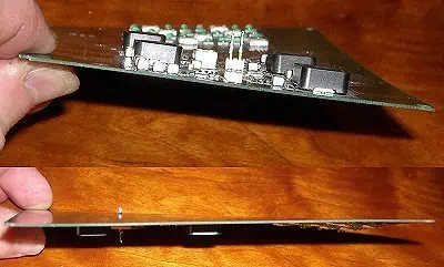
Printed circuits or PCBs are getting thinner and smaller as they get more complex (prevent PCB bent). But, occasionally, we run into the issue of a bent PCB or a warped board, even if a minor curve might also impair the performance of a PCBA.
The “Performance and Specification Standard for Rigid PCBs” states that the SMT boards’ maximum permitted warping and bending is 0.75%. Nowadays, the warping tolerance range for double-layered or multi-layered electronic assembly facilities with a 1.6 mm thickness is typically 0.70-0.75%. A lot of BGA and SMT boards need 0.5%. Several electronics firms are pushing for a 0.3% warping norm.
Bent PCB Test Method
Placing the PCB on a validated platform and inserting a test pin into the area of the board that exhibits the greatest warping will allow you to determine the degree of warping. It divides the test pin’s diameter by the height of the bent edge of the board.
PCB deformation requires visuals of the substance, distribution, structure, and processing processes from a number of angles. As in the research, this article’s deformation may occur for a number of causes, and many ways to improve are considered and explained.
Because the surface area of copper on the PCB is not homogeneous, the plate will distort and flex.
PCB also has the ability to heat up and cool down. But when these vast copper foil areas cannot be distributed evenly over the same board, it will result in uneven cooling and heat speed. PCBs also have the ability to experience different types of deformation and stress depending on the board’s temperature at the time. If this temperature is too high, the board may become distorted.
The link marks on every layer of PCB (vias, TH) will restrict the board’s shrinkage.
Today, the majority of PCBs are laminated, and the connection points between layers are like rivets. Connecting points are further divided into holes, buried holes, and blind holes. Connecting points limit the effect of cold on the board and can also implicitly result in warping and plate bending.
There are numerous reasons that cause the issue of PCB bending. The most frequent one occurs when the tension placed on the PCB exceeds the stress that the PCB can sustain; the Board bending problem manifests itself right away.
The “high temperature” is the main source of stress when PCBs are processed via the reflow hot oven for Surface-Mounting Technique. The PCBs will become softer at high temperatures due to the CTE factor, as well as their feature of thermal contraction and expansion. If somehow the temperature exceeds the PCBs’ maximum TG value, the Circuit boards will bend.
Rarely do PCB designers take the edge of the PCB copper into account. The Circuit board will readily flex in high-temperature conditions if the Circuit edge does not have copper.
Also, if the SMD electronic components are hefty and the PCB size is rather large. The weight will create the Circuit board bending problem.
The PCB’s structure will be destroyed by the V-cut used to neatly separate the boards, and this will quickly lead to the Board bending problem.
Based on over 18 years of manufacturing and installation expertise with PCBs, we’ve compiled some lessons learned and suggestions on how to avoid PCB bending that we’d like to share with you.
1. Use High TG Material
The average temperature (TG) is above 130 degrees, the average high temperature (TG) is above 170 degrees, or the average medium temperature (TG) is above 150 degrees.
Increasing the TG improves the PCB characteristics of the material. This includes humidity resistance, heat resistance, stability, and chemical resistance. There are additional high TG uses, particularly in the process of lead-free. This is because the plate’s thermal resistance improves with increasing TG value. The greater TG value guarantees that the Circuit is somewhat resistant to deformation and changes caused by the outside environment, which can prevent the PCB from bending or warping.
2. Board Thickness
Boards that are thicker will be more rigid and simpler to keep straight. Reflow soldering needs to install several components on PCB. The thick base is difficult to distort when the load and temperature change. Maintaining the thickness of the board at 1.6mm can greatly lessen the likelihood that the board will deform.
3. Evenly distributed Copper
PCB assembly finishes in a panel format. If the copper is distributed throughout the board side and connected areas after it has been panelized (positions that will be removed after assembly), the total PCB panel must be maintained. When the copper’s density and thickness are identical, warping the plate after assembly is difficult.
4. Panelize Way
It is important to keep the panel’s size in mind when designing it, as well as to keep its shape consistent and stable. A panel that is too lengthy will break in the center.
5. Reduce Reflow Temperature
If an unequal or excessive strain applies to the PCB, it will deform. From where does the board’s tension come? In the soldering reflow process, the biggest stress arises from temperature. Together with physical reasons that induce thermal expansion in all materials, the temperature does not soften but also bends PCB. As a result, it is thought to be the primary reason for PCB warping.
6. Modify Design
There will be a lot of vias, blind buried, and blind holes on multilayer PCBs. These soldered nodes encourage the development of circuit warpage and restrict the alterations that the PCB experiences when subjected to high temperatures and pressure. As a result, some layout engineers will label some spaces in the substrate’s absence of copper wiring in order to aid in the PCB’s heat dissipation.
7. Reflow Carrier
The reflow soldering carrier can decrease the PCB warping and bending. This is because it has the ability to hold the PCB despite the fact that heat will extend it. The PCB regains its warmth and hardness after the reflow process of soldering is finished. This procedure is restricted to the carrier of reflow and won’t take place in all cases. We also can create fixtures to aid in fixing, although doing so entails manually replacing pallets.
8. Do Router Not By V-Cut
If we create the panel using a V-cut, the PCB’s general structure will deteriorate, making the panel bending and warping more likely. So, we may utilize routing rather than V-cut if it’s permitted in production.
The rate of prepreg shrinkage in the weft and warp directions really isn’t equal after laminating. While trimming and laminating, you must differentiate between the weft and warp directions. If not, the completed board could deform after lamination, which would be challenging to fix even with pressure.
The prepregs’ longitude and latitude are sometimes not differentiated and are stacked arbitrarily during lamination. This results in the multilayer Circuit board bending for a variety of reasons. How are the weft and warp distinguished? The prepreg is folded in the direction of weft for breadth and the direction of warp for thickness.
In the case of copper foil, the warp is on the short end, and the zonal is on the long end. If you’re unsure, you can ask the supplier or manufacturer.
10. Semi-Solidified Symmetrical
For instance, on a six-layer PCB, the semi-solidified panels should be in layers one and two, five and six. Prepregs and multilayer cores ought to utilize supplies that come from one vendor.
On the A & B edges of the outermost layer, the space of the pattern lines ought to be as similar as feasible.
This PCB will readily deform after etching if surface A is a big surface of copper and surface B is just a few pattern lines away.
If the line areas on both sides vary too much, users can add a few individual grids over the rare sides to adjust.
11. Baking Board
Prior to trimming the copper-clad panel, dry the panel to eliminate any moisture that might have crept in during prolonged storage (150 degrees Celsius, 8 x 2 hours).
Also, it is important to thoroughly dry the epoxy in the panel, which will further reduce any leftover tension and aid in keeping the board from warping.
Currently, numerous double and multi-layered PCBs still conform to the phase of baking prior to or after blanking. Nevertheless, certain plate manufacturers are an exception. The time necessities for drying panels in different PCB factories currently range from 4 to 10 hours. We propose selecting depending on the quality of the PCB generated and the needs of the customer for the warpage. These approaches are possible after cutting the block into panels, baking, or chopping the entire block. After cutting and baking, dry the circuit boards. After cutting and baking, dry the circuit boards.
Copper conductors are used to link electronic board components electrically. These boards provide mechanical support to suit electronic gadget components. Before we go into details on how to make a electronic board, let’s first consider what an electronic board means.
What Does an Electronic Board Mean?
This bare board in which you provide with the layout data as well as which, after we have given this to you, you use it to place your components is known in the industry as printed circuit board.
Utilizing conductive paths, tracks, as well as signal traces that are etched out of copper sheets and laminated to a substrate that is non-conductive, a PCB, is employed to electrically link as well as mechanically support the electronic components.
Whenever the board merely has copper tracks as well as features but no active devices or capacitors or resistors have been fabricated into the board’s actual substrate, then it is referred to as the PWB (printed wiring board or the etched wiring boards.
Though much more accurate but distinguishable from what can be recognized as a genuine pcb, the term PWB has generally lost favor with many people with the line between wiring and circuit gotten more hazy.
Currently, every one of the basic commercially made electronic devices employ printed circuit (wiring) boards, which enable completely automated assembly procedures that weren’t feasible or viable in older tag type processes of circuit assembly.
Although the stage of CAM engineer constitutes the primary step during PCB fabrication, the circuit board design can be described as the preliminary step of the process of etching.
Designers choose the proper power supplies, processors, and other components after analyzing the needs. Make a plan that satisfies all requirements.
The board must, however, be strictly consistent with the layout of the PCB that the designer generated using Circuit board design software. This contract manufacturer must be informed about the software version used for the PCB design that was used to create the circuit, as a designer, since this helps to prevent issues brought on by inconsistencies before the circuit board is made.
Print the finished design onto transfer paper. Ensure the design will fit on the paper’s glossy side.
Circuit Board Design Output
Although alternative databases and formats are accessible as well, data often comes in an Extended Gerber file called RX274x or simply Gerber), which happens to be the most used software.
Gerber files, which all store crucial information enabling synthesis, such as drill patterns, copper trace layer, component symbols, as well as other parameters, may need to be generated using various Gerber file generating processes depending on the Circuit board design program being used.
All the various components of such design are examined to make sure no problems exists after the PCB design layout has been imported in the extended gerber program.
Drawing of the PCB File – PCB Design Film Creation
The following step has to do with printing the PCB when it has been finalized. Normally, this is carried out in a dim space with regulated humidity and temperature. Punch holes within every PCB picture film layer at specific locations to align the various layers. The images for the copper routes were created with the aid of this movie.
Advice: As a Circuit board designer, please remember to inform your manufacturer to perform DFM inspection after generating the Circuit board schematic file.
PCB printing often uses a specialized laser printer termed laser photoplotter; while it’s a laser printer, this differs from a Laserjet printer in many ways. Nevertheless, this shooting method seems to be no longer adequate due to downsizing and technological innovation.
Transfer of the Inner Layer Imaging: Printing of the Inner Layer
Only boards having at least three layers can complete this step. Straightforward, two-layer boards don’t need to be drilled. Steps are added when using multilayer boards.
This preceding step’s film generation was intended to graph its copper journey. The graphics gotten from this film are now ready to be printed on this copper foil. This copper needs to be cleaned first.
Maintaining cleanliness is essential when building PCBs. After being cleaned, this copper-faced laminate gets delivered to the decontaminated area. To prevent opening or shorting of the completed PCB, be sure that there’s no dust settling on the PCB surface.
The photosensitive film coating known as photoresist is applied to its cleaning panel. This copper design is defined by the photoresist being hardened by the printer’s strong UV lamp via a transparent film.
Etching can be described as the technique of removing surplus copper from the circuit board during PCB fabrication. All that is left on this board after removing the non-circuit copper is the surplus copper. A desirable circuit layout is therefore realized. This base copper, also known as starting copper, gets taken from the circuit board throughout this procedure.
Unwanted copper is eliminated from the board, while required copper is protected by the hardened photoresist, and the unwanted copper is removed from unhardened photoresist. To remove the extra copper, you rinse with acid etchant. Nonetheless, we still want this photoresist layer to completely enclose any residual copper.
Prior to the etching procedure, lithography is used to transfer the circuit image needed by a designer on the PCB. This creates a framework that helps in determining that part of copper that needs to be taken out.
Alignment of the Layers
The layers appear in pairs in order to create a Circuit board “sandwich,” which includes a thin copper foil layer that covers the bottom and top surfaces of the board. A “prepreg” piece would be put between every pair of layer to aid in the bonding process. Prepreg can be described as fiberglass material which has been impregnated using epoxy resin. It melts when laminated because of the pressure and heat involved. The prepreg will glue the layers in place as it cools.
Prepregs, or alternate layers of the fiberglass epoxy-impregnated sheets, are bonded with conductive cores utilizing the hydraulic press and at high pressure and temperature to create multilayer Boards. Prepreg is melted and joined together under heat and pressure. The resulting material, after cooling, will utilize the same process for manufacturing as the double-sided circuit boards.
Drilling of Holes: For the Connection of the Components
The PCB has been drilled with mounting holes, through holes, as well as other holes (which are usually inside the panel stack, with respect to the deepness of the drilled holes). Complex optics offer accurate as well as clean hole walls, which are essential.
The X-ray finder can recognize the proper drilling target point and locate the drilling target’s location. After that, drill pilot holes in the proper places to anchor the stack before drilling a succession of more precise holes.
To maintain a proper drill hole, the technician installs a buffer material beneath its drilling target prior to drilling. Its drill exit is shielded from any unintended ripping by a exit material.
AOI Inspection (For Multilayer PCBs Only)
It is not possible to detect flaws in its inner layers after lamination. Hence, before gluing and laminating, the panels go through an automated optical examination. The machine uses the laser sensor to scan the layer and compare it with the initial Gerber file so as to identify any discrepancies.
The layers must be verified for alignment after they are ready and clean. With the aid of the previously-drilled holes, the outer and inner layers will align. To keep its layers in place, the optical punch punches a pin via the hole. This process of inspection then starts to make sure there aren’t any flaws.
After plating, the photoresist on the panel becomes undesired and must be removed. This is accomplished via a lateral technique that exposes the base copper of the panel to an underlying etching process for elimination while successfully removing the photoresist with a solution of soda ash.
Tin currently shields the optimal copper. Remove any unnecessary copper that is exposed and any copper that is buried beneath the remaining resist layer. In order t o remove the undesired copper during this etch, you utilize the ammonia etchant. Tin also guarantees the current stage’s need for copper.
Conducive regions and links have now been classified legally.
Solder mask
This solder mask is applied using the UV exposure procedure that is akin to photoresist to protect your board throughout assembly. All of the circuit board’s surface will be covered by the solder mask, excluding the functional parts and metal pads.
marks for component reference as well as other circuit board markings will be silkscreened onto the circuit board asides from a solder mask. The board can be baked in the oven to cure the solder mask as well as the ink for screen printing.
The exposed metal surface of the board is going to have a polish. This facilitates soldering operations throughout assembly and protects exposed metal. The surface finish gets exemplified via HASL. Before dipping the board inside the molten solder baths, flux your board to get it ready for solder. High pressure of hot air is used to remove the excess solder out from the holes after this board has been removed from your solder bath and to smooth this solder onto the metal’s surface.
Application of a solder mask
Before applying solder resist to the board’s two sides, epoxy solder ink is put to the panel. This solder mask would let through the Ultraviolet light that the board receives. The piece that was covered is still soft and must be taken off.
The board should then be baked to cure any solder mask.
Because it is easy on the eyes, green was selected as the typical color of solder mask. All processes are manually reviewed before such a machine could inspect the PCB during manufacture and assembly. This overhead lighting that technicians utilize to examine circuit boards is beneficial for human eyes because it does not reflect the greenish solder mask.
Silkscreen
The technique of printing every important information on the surface using profiling or screen printing on the circuit board like name of company, manufacturer ID, debug points, component number, etc. This is very important when repairing and servicing.
Important information gets printed upon that board throughout this process, making it an essential phase. The final curing and coating processes will be applied to the boards after they are finished. This printing of legible identification information, such as 1-pin locators, part numbers, as well as other markings, is known as screen printing. Inkjet printers can be used to print these.
Moreover, it is the most sophisticated method of producing PCBs. In order to identify test points, components, PCBA and PCB part numbers, company logos, warning symbols, manufacturer markings, date codes, manufacturer markings, as well as almost finished boards were printed using easy-to-read lettering.
The final curing and coating stage for the PCB is at last reached.
Flying probe test for electrical testing
The technician would run a functionality test of your board as a last-ditch precaution before inspection. They now perform an automated approach to verify the PCB’s functionality and conformity to the initial design.
Flying probe test, which is an advanced form of the electrical testing, is typically used to examine the electrical functions of every net on such an uncovered circuit board.
Analysis of the production and the V-score
These individual boards could be removed from this panel once the circuit board panel must have undergone electrical testing. A CNC router or machine carries out the procedure to shape as well as resize every board from a panel towards the needed specifications.
According to the total thickness of every panel, several panels could be stacked three or two high to accelerate the procedure and use router bits that are typically between 0.030 and 0.093 in size.
Using different head sizes of milling, the CNC machines may also produce grooves, bevels, and chamfers during the operation.
Final Examination – PCB Quality Assurance
The inspector must perform an extra inspection of every PCB during the process’s last stage. Check the Circuit board visually for adherence to the admission requirements. Utilizing manual and AVI visual inspection Compared to the inspection of the human eye, compares PCBs into Gerber, and yet still needs human verification.
To ensure these items meet the customers’ criteria, all orders would also be thoroughly inspected, including solderability, dimensions, and other factors. Additionally, goods on the board is subjected to a perfect quality audit before even being packed for transportation.
There are many potential for Circuit board failure concerns to develop due to the complexity of Circuit board design as well as manufacturing processes. A number of the failures are the consequence of design errors, such as inadequate clearances or inaccurate measurements that can impair the end product’s functionality. Everyone else might be the result of manufacturing process issues, such as over-etching or drilling mistakes, which can both be disastrous.
Fortunately, the majority of these mistakes could be avoided having knowledge of the manufacturing procedure, consideration for it, and knowledge of the typical PCB manufacturing problems. Connection problems, component failure, and other concerns related to circuit board can be avoided by adhering to a variety of general design guidelines and considerations.
Plating Voids
Copper-coated holes on the PCB are known as plated through-holes. From one of the sides of your PCB to the second side, electricity can travel through these holes. This PCB board manufacturer drills these holes via the PCB board, completely piercing its base material. Then, using an electroplating procedure, a copper foil layer as well as copper coating is applied to the material’s surface as well as along these holes’ wheels.
Deposition is the procedure used in this step to deposit a thin electroless copper layer to the printed circuit board. Following this, further copper layers will be applied, and the image of the circuit is etched.
Plating voids, which are essentially holes or gaps in the circuit board plating, are usually the consequence of issues with the process of deposition. The plating voids seem to be especially problematic since through-hole plating flaws make it impossible for the electrical current to pass via the hole, leading to a flawed product.
Slivers
When making circuit boards, slivers, which are tiny wedges of solder mask or copper created during the circuit board manufacturing process, can be quite problematic. These fragments, which are frequently created during the process of etching, can happen in any of these ways explained below.
Slivers could first be created by etching away an exceptionally thin, long, characteristic of the solder mask or copper. This sliver occasionally separates before dissolving completely. Inside this chemical solution, these disconnected slivers may float around or even settle on some other board, creating an accidental link.
Cutting a part of the circuit board too deeply or narrowly is another approach to create slivers. Even when they’re intended to remain connected to the circuit board, a material of silver can entirely or partially separate from it if the etched section becomes too small or its etching is too deep, leading to either the peeled-back silver or a floating sliver. Both possibilities could have extremely detrimental effects on the functionality of your circuit board.
Acid Traps
A circuit’s acute angles are frequently referred to as “acid traps.” The acute angles help in trapping acid throughout the process of PCB etching, causing acid to accumulate in the angle’s nook, which is why they are known by this name. Because of the angle, this same acid stays in a corner that is longer than is necessary by design, eating away more material than is planned. Due to this, this acid can weaken a connection, rendering the circuit flawed and leading to subsequent, more severe issues.
The majority of designers were told to stay away from acute angles since they are conscious of the issues they can cause on the circuit board. Nonetheless, errors do occur.
Solder Mask Missing Between the Pads
The copper layer of the PCB is followed by a solder mask layers. To protect its copper traces against contact made with other metals, solder, and conductive bits, the solder mask gets placed on the copper layer’s top. Moreover, it serves as a shield between the copper as well as the environment, preventing corrosion as well as shielding the people handling the PCB from being electrocuted. Components are typically soldered onto the areas of metal known as pads that such solder board has left exposed.
This solder mask between pads may be absent entirely or partially on some printed circuit boards. By exposing excess copper than what is required, this raises the risk of solder bridges unexpectedly forming between pins while assembling.
As a result, the circuit board’s functionality and durability may be adversely impacted by a short as well as lower corrosion protection.
Copper-To-Edge Clearance Not Enough
Copper, which serves like an active constituent of PCBs, is a very conductive metal. But copper also happens to be a somewhat soft metal that is prone to corrosion. The copper gets covered with various materials to stop corrosion and guard against environmental contact.
But, if indeed the copper becomes too near to its edge during the trimming of the PCB, some of the coating may also be removed, revealing that copper layer beneath. Many issues with the board’s functionality may result from this.
Leakage of Chemicals
Another typical problem with PCBs is chemical leakage, which can occur due to the different chemicals utilized when manufacturing PCBs.
The leaking of such chemical residues over time might corrode the metal parts of the circuit boards and lead to short circuits.
Conclusion
By now, you should understand how to make a electronic board. Several electrical parts make up the electronic board. Each part is essential to the operation of the electronic board. PCBs also feature holes where each electrical component needs to be installed. PCBs play a significant role in any electronic device.
When electromagnetic radiation from the environment prevents an electronic system or equipment from functioning normally, this is known as electromagnetic interference (EMI). EMI can come from artificial and natural sources, including electrical devices, power lines, radio and television transmissions, and natural sources like lightning.
EMI can negatively affect electronic devices, including system failure, malfunctions, and data mistakes. In addition, EMI can occasionally be dangerous, for instance, by interfering with aviation systems or causing medical equipment to malfunction.
A device’s ability to withstand an amount of EMI without malfunctioning depends on several variables, including the device’s susceptibility to electromagnetic radiation, the frequency and power of the EMI source, and the environment in which the device operates.
Magnetic EMI (Electromagnetic Interference) is a type of interference that arises when magnetic fields created by one electronic device or circuit cause unwanted electrical impulses in another nearby device or circuit. This can occur when an adjacent circuit experiences undesirable noise or distortion due to the current created by the changing magnetic fields of one circuit.
Sources of magnetic EMI include motors, transformers, power lines, and other electrical devices that produce magnetic fields. Data mistakes, communication breakdowns, and other issues may result from interference with the performance of surrounding electronic equipment.
Capacitive EMI:
Capacitive EMI happens when electrical energy moves from one circuit to another via a capacitive coupling mechanism. For example, capacitive coupling takes place when two conductors that are separated by a dielectric material are close enough to one another for an electric field to form between them.
Capacitive coupling can introduce undesired electrical noise or interference into an electronic circuit in EMI. This interference may appear as spikes, hiccups, or other irregularities that impair electronic device functionality.
Radiated EMI:
Emissions of electromagnetic waves into the surroundings, known as “radiated EMI,” are electromagnetic interference. Transmissions from radio and television, electronic devices, and power lines are just a few examples of the many things that might produce this kind of EMI.
Surrounding electronic systems can have a system failure, data mistakes, or malfunctions when radiated EMI is present. Shielding and filtering are two methods that can help lessen radiated EMI’s effects.
Conducted EMI:
Conducted EMI is electromagnetic interference that travels via conductive paths like wires, cables, or power lines. EMI sources include switching power supplies, motors, and other electrical devices that produce high-frequency noise.
In a circuit, conducted EMI can result in malfunctions, data errors, or total system failure. Shielding, filtering, and grounding are just a few strategies employed to lessen the effects of conducted EMI.
EMI shielding
EMI (Electromagnetic Interference) Shielding is the technique of enclosing electronic devices or systems in conductive or magnetic materials to shield them from unwelcome radiofrequency interference (RFI) or electromagnetic interference (EMI).
Metals (such as copper, aluminum, or steel), conductive polymers, or conductive fabrics can help create EMI shielding. These substances form a barrier that blocks electromagnetic waves from going through and instead reflects or absorbs them.
The frequency of the electromagnetic waves, the kind of shielding material employed, the material’s thickness, and the shielding enclosure’s design are only a few of the variables that affect how successful EMI shielding is.
Applications for EMI shielding span from electronic devices like computers and cellphones to aerospace and military systems. The equipment must be free from external electromagnetic radiation interference to prevent failures.
Overall, electromagnetic interference (EMI) shielding is a crucial component of electronic design because it supports preserving the integrity and dependability of electronic systems in the presence of EMI.
Due to its role in preventing unwelcome electromagnetic energy from interfering with electronic systems, circuits, and devices, EMI (Electromagnetic Interference) shielding is crucial.
Electromagnetic radiation surrounds us. They can come from several sources, such as power lines, radio waves, cell phones, and other electrical gadgets. As a result, sensitive electronic components may experience malfunctions or complete failure due to this energy’s interference with their normal operation.
EMI shielding functions by erecting a wall that absorbs or blocks electromagnetic energy. Conducive materials, including metals or conductive coatings, can help to achieve this.
Medical equipment, military and aerospace equipment, telecommunications equipment, and consumer electronics are just a few examples of the many applications where EMI shielding is essential. Without adequate EMI shielding, these devices may perform worse, be more susceptible to interference, or fail.
Overall, EMI shielding is crucial when designing and manufacturing electronic systems and devices since it ensures their dependable and secure operation.
Mechanisms of EMI Shielding
Shielding from electromagnetic interference (EMI) operates by deflecting or absorbing the waves. To provide EMI shielding, several mechanisms can be helpful:
Magnetic Shielding:
Utilizing materials to prevent or lessen the electromagnetic field generated by electronic devices is known as electromagnetic interference (EMI) shielding. Due to interference or function disruption caused by EMI, electronic devices might suffer injury and perform poorly.
High magnetic permeability materials are helpful in magnetic EMI shielding to reflect or absorb the magnetic field. By forming a path of low magnetic resistance around the electronic component or device, magnetic EMI shielding helps to deflect or absorb the magnetic field.
High magnetic permeability is a characteristic of the materials used for magnetic EMI shieldings, such as nickel, iron, and cobalt alloys. Due to a characteristic of these materials known as “magnetic hysteresis,” the energy from the magnetic field can be absorbed and dispersed.
Power supplies, transformers, and motors are just a few electronic components that can benefit from magnetic EMI shielding. In addition, electronic devices can run more effectively and efficiently without interruption from outside magnetic fields by adopting magnetic EMI shielding.
Faraday Cage:
A barrier called a Faraday cage is ideal for blocking electromagnetic interference. (EMI). It bears the name Michael Faraday after the British scientist who developed the underlying idea in the early 19th century.
A Faraday cage comes from a conductive mesh of copper, aluminum, or steel grounded electrically. Electric currents are induced in the conductive material when electromagnetic waves, such as radio or microwaves, contact the cage. This conductive material creates an opposite electromagnetic field, which cancels out the first wave. This efficient EMI shield prevents electromagnetic radiation from entering or leaving the cage.
Faraday cages are helpful in several applications to stop EMI from interfering with the operation of electronic equipment and medical devices. They also shield houses and other structures from electromagnetic interference and lightning strikes.
Faraday cages are a crucial tool for many businesses that rely on delicate electronic equipment because they offer a key method for EMI protection.
Two related ideas help to stop electromagnetic interference from impacting electronic devices: grounding and EMI (electromagnetic interference) shielding.
An interference type brought on by electromagnetic fields is known as EMI. Radio waves, electrical circuits, and other electronic equipment are only a few potential causes of this interference. In addition, electronic devices may experience issues when EMI is present, such as signal disruption and data transmission failures.
The amount of electromagnetic radiation that can harm electronic devices decreases via EMI shielding. This shielding often consists of conductive material that may absorb or reflect electromagnetic radiation, such as copper or aluminum. To shield an electronic circuit or device from EMI, place shielding around it.
An essential component of EMI shielding is grounding. A grounded EMI shield permits any stray electromagnetic radiation that enters it to route back to the ground rather than harming the object intended to shield. The shield can be made more effective at reducing EMI by being grounded.
As a result of its role in ensuring that errant electromagnetic radiation moves away from electronic devices, grounding is a crucial part of EMI shielding. In addition, reduced interference can enhance the performance and dependability of electronic devices. Hence EMI shielding is crucial.
Absorption:
Absorption The amount of electromagnetic energy that enters a certain space or equipment can decrease using the EMI (Electromagnetic Interference) shielding technique. EMI shielding aims to build an electromagnetic barrier to prevent unwanted signals from interfering with delicate electronic equipment.
Absorption EMI shielding blocks electromagnetic radiation by absorbing and releasing it as heat. High conductivity and magnetic permeability materials, such as ferrites, metals, or conductive polymers, achieve this.
An EMI shield blocks electromagnetic waves, causing a current to flow through the shield’s material. This opposing magnetic field then traps the electromagnetic energy. As a result, the intensity of the wave penetrating the barrier reduces due to the energy coming out as heat.
The frequency of the electromagnetic radiation, the thickness and make-up of the shield material, and the shield’s design all affect how well absorption EMI shielding works. For example, the ability to absorb electromagnetic radiation will improve by using a thicker shield of high-conductivity materials.
Absorption EMI shielding is frequently helpful in stopping electromagnetic interference from interfering with the operation of electronic devices like laptops, tablets, and smartphones. Additionally, it is essential in military and industrial settings to shield critical equipment from outside electromagnetic interference.
Reflection:
In contrast to blocking or absorbing electromagnetic waves, reflection EMI shielding works by reflecting them away from the electrical device. A conductive material that reflects the waves, like a metal plate or foil, helps to do this.
When electromagnetic radiation is exceedingly intense or challenging to block using conventional techniques, reflection EMI shielding can be beneficial. However, it is crucial to remember that reflection EMI shielding may not always be successful and that other types may be necessary for some circumstances.
Generally speaking, reflection EMI shielding is a crucial way of shielding electronic equipment from electromagnetic interference and can be a valuable supplement to other shielding techniques.
Electronic equipment and devices are safe from external electromagnetic interference, which can lead to malfunctions, interference, or data loss, using EMI (Electromagnetic Interference) shielding. EMI shielding materials help prevent electromagnetic waves from spreading and lessen electromagnetic noise. High conductivity and magnetic permeability are typical characteristics of the materials used for EMI shielding, generally divided into conductive and magnetic materials.
Carbon-based materials:
Due to their special qualities, carbon-based materials are in use more frequently in EMI (Electromagnetic Interference) shielding applications. Graphene is the most promising material with its excellent conductivity, outstanding mechanical strength, and large surface area. Additionally being investigated for EMI shielding purposes are carbon nanotubes (CNTs). However, carbon-based materials can be expensive and time-consuming to produce and manufacture, and environmental conditions like temperature and humidity can impact how well they work.
Conductive polymers:
Due to their electrical conductivity, conductive polymers are a new family of materials utilized in EMI (Electromagnetic Interference) shielding applications. In addition, they are pliable, lightweight, and simple to mold into intricate designs. They can improve through doping, but the dopant’s selection and concentration can impact other qualities like mechanical strength and stability. However, oxidation or exposure to environmental conditions over time might cause a decline in their performance.
Metals:
Due to their high conductivity, metals like copper, aluminum, nickel, silver, and gold are frequently helpful for EMI shielding. In addition, because metal materials are good at reflecting or absorbing electromagnetic waves, they are frequently helpful in EMI (Electromagnetic Interference) shielding. The frequency range of the electromagnetic waves for shielding and the required shielding level will determine the thickness and size of the metal material utilized. Depending on the particular application’s needs and the surrounding environment, other materials, such as conductive coatings and textiles, can also be helpful for EMI shielding.
A disruption caused by electromagnetic radiation that interferes with an electrical circuit is known as electromagnetic interference (EMI). Electrical devices encounter this interference, and EMI shields help to stop or lessen its effects. EMI shields can consist of conductive coatings, metal enclosures, gaskets, and absorbent materials, among other things.
Shielding Fabrics
Clothing and other textiles can benefit from EMI shielding by using shielding fabrics. These textiles can be woven into various patterns to give various amounts of EMI shielding. Additionally, they often consist of conductive materials like silver or copper. In addition, shielding materials are frequently helpful in areas like telecommunications and the military where workers face high quantities of electromagnetic radiation.
Shielding Tapes
Cables and wires can be safe from EMI by using shielding tapes. We can swap the cables in these tapes, which are commonly copper or aluminum, to create a conductive route that aids in the dissipation of electromagnetic radiation. The automotive, aerospace and telecommunications industries are just a few places where shielding tapes might be essential.
Absorptive Materials
Materials that absorb electromagnetic energy will do so rather than reflect it. These materials are frequently helpful in applications, such as power supplies and converters, where internal EMI generation occurs. Ferrites, ceramic materials containing iron oxide, are the most typical absorptive substances.
Gaskets
Gaskets are essential when two surfaces, like a door and a frame, need sealing off. They are essential in EMI shielding to provide a conductive route between two surfaces and block the passage of electromagnetic radiation. Silicone, rubber, and metal are just a few materials that can help to create gaskets.
Metal Enclosures
Metal enclosures are yet another typical EMI shielding material. These enclosures can fit a variety of electronic equipment and consist of aluminum, steel, or copper. Metal enclosures function by enclosing the electronic gadget in a Faraday cage that blocks electromagnetic radiation from entering or exiting.
Conductive Coatings
As an EMI shield, conductive coatings are frequently helpful. These coatings offer a conductive route that aids in the dissipation electromagnetic radiation on the surface of electronic equipment. Silver, copper, and nickel are the most often helpful materials for conductive coatings. We can apply these coatings in several ways, including electroplating, dipping, and spraying.
The Raspberry printed circuit board is a distinctive type of printed circuit board used in producing Raspberry computers. Raspberry is a computer developed by the Foundation of Pi. Each model in the series has its unique features and capabilities. Therefore, it is essential to provide more detailed information about each of the Raspberry models.
What is Raspberry PCB Layout?
The Pi printed circuit board is a credit card-sized computer board that features a combination of castellated and through-holes with a pin header pitch. It is designed for various tasks such as word processing, gaming, and spreadsheets due to its compact size.
A Pi Foundation created the Raspberry technology, which has been present since 2012. The primary goal was to enhance learning, innovation, and experimentation. The Pi printed circuit board is the portable board utilized in Raspberry computers.
Most mobile phones manufactured in the 21st century contain Pi-printed circuit boards. ARM technology has been a common feature in many of these phones. There are two models of
Pi circuit boards available: Model B & Model A. Model A takes less power than Model B and does not have an Ethernet port, while Model B has an Ethernet port.
The Raspberry utilizes various technologies, and the development of the Pi PCB led to the creation of the computer module.
Designing a Raspberry PCB printed circuit board involves tailoring a board to your specific requirements. This process is simple and cost-effective and can be achieved using compute module production kits. By creating a custom Raspberry printed circuit board, you can ensure that it meets your exact product specifications while retaining the highest level of design flexibility. Additionally, you can select the components you prefer using online equipment. A benefit of the Raspberry printed circuit board is that it’s made from scratch.
Using a compute module, it is possible to design a Raspberry printed circuit board within a matter of hours. However, it is important to carefully select the functional elements you wish to include in your design. With a compute module, you can customize the layout & display ports of your custom PCB to suit your needs.
When creating a Raspberry printed circuit board, there are several key factors to consider that will impact the requirements of your circuit board. Speed, size, memory & model type are all important considerations during the design process.
Specifications of Pi Pcb Layout
A Raspberry printed circuit board comprises numerous components, including GPIO pins, CPU, RAM, processor, & graphics chip. Additionally, this board features many interfaces for connecting with external devices. To enable startup, the Raspberry printed circuit board needs mass storage, typically provided by an SD card. It allows the board to boot up from the SD card, much like a computer starts up and loads the Windows operating system.
· Memory
The Raspberry Model A board has 256MB of SDRAM, while Model B has 512MB. Compared to other computers, the Raspberry’s memory capacity is relatively small. While typical PC RAM is also available in gigabytes, the Raspberry’s RAM ranges from 256MB to 512MB.
· GPU
A Raspberry circuit board includes a GPU, a specialized chip designed to improve image processing capabilities. The Broadcom VideoCore IV GPU is integrated into the Raspberry PCB, and it supports OpenGL for enhanced graphics performance.
· GPIO Pins
General Purpose Input/Output (GPIO) pins facilitate communication between the Raspberry and other electronic devices. These pins can be programmed to accept input & output commands, enabling them to communicate with various external sensors and other components. For example, a temperature sensor can be connected to the GPIO pins to facilitate data transmission.
· Central Processing Unit (CPU)
The CPU serves as the central processing unit, or “brain,” of the Raspberry PCB. It executes computer instructions using mathematical & logical functions. In particular, a Raspberry uses an ARM11 processor to handle these tasks.
· Power source connector
The shield features a minor switch on its side, and the energy source connector allows for connecting an external energy source.
· Ethernet Port
It is a gateway for connecting with extra devices. Using an Ethernet port, the Raspberry can connect to the house router and get internet access.
Factors to Know when choosing Raspberry Pcb Layout
· Scalability Needs
The Raspberry circuit board is not a commercial product, so there are currently no practical replacement boards available with different performance specifications. If you complete the development and then realize the demand for different specs, it’s important to consider designing for adaptability as you go from the stage of prototyping to a more flexible part of the product development process. It means planning for potential modifications and ensuring that your design can accommodate changes in performance specifications without requiring a complete redesign. By designing for adaptability, you can ensure that your product can evolve and meet changing market demands over time.
· Development Support You Need
The Raspberry circuit board is primarily supportable by online communities & forums, and its strength lies in support rather than professional production support. If you have tight deadlines, you can launch the product with community support. Still, if you require dedicated support, you may need to seek professional development resources.
It is advisable to schedule the components of your product and assess the level of support available before making a final decision. It is often advisable to test the performance of the components to ensure that you will achieve the outcome of your final product.
Advantages of Pi Pcb Layout
The Raspberry printed circuit boards provide numerous advantages, making them well-suited for various applications.
· Supports various codes
One of the most significant advantages of Pi PCBs is their versatility. But Arduino offers a more comprehensive range of capabilities. Raspberry PCBs act as single-board computers, but they also offer a Linux environment that supports coding in any language. These boards are particularly popular due to their compatibility with different codes.
· Peripheral support
Raspberry PCBs are equipable with GPIO pins, which are beneficial for interfacing with hardware projects. These pins offer a deeper understanding of component interfacing. The Raspberry’s abundant GPIO pins allow for the connection of multiple digital sensors.
· Faster processor
Compared to other boards, Raspberry circuit boards have a fast processor of 1.6 GHz. Having a faster processor results in better performance. Raspberry PCBs provide a fast processor at an affordable price point.
· Several sensors
The Raspberry boards come with a plethora of GPIO pins, which allows them to support multiple sensors simultaneously. As a result, they can be easily connected to various displays, modules & sensors, making them a versatile option for different projects.
· Serves as a portable computer
One of the most significant advantages of Pi is its portability. When combined with a display, it can function as a pocket computer. So Raspberry circuit boards support WiFi, enabling you to perform computer tasks on the go.
The Pi model, 4 of raspberry, can effortlessly handle all of these lightweight processes without putting a strain on its power & processing capabilities.
While the Pi model 4 of raspberry shares some similarities with your smartphone’s hardware, the software aspect of the two differs significantly. As you may already know, Android smartphones operate on a GNU/Linux system, an open-code OS that can be customized to meet your requirements. There are various versions of the Linux OS available, and the one you have on your cell phone is one of them. On the other hand, installing the Pi model 4 of raspberry is a completely distinct version. Nevertheless, having this OS enables you to:
Enjoy a desktop-class browsing experience on the board
Install and use apps for editing pictures, videos, and audio on the board
Utilize Raspberry Pi 4 for web pages, home file servers, or FTP hosts.
Starting is simple; you only need a monitor, keyboard, and mouse.
· Home Theater
Despite its small size and low power consumption, the Raspberry PCB model 4 Pi board can still support USB storage devices like hard drives. This makes it an ideal replacement for a home theater computer.
By utilizing specialized software like OSMC, it is possible to install and utilize Xbox-style applications via KODI. Additionally, it is possible to control all functions using a remote, eliminating the need for a keyboard and mouse.
All the software needed to turn your Raspberry PCB model 4 Pi into the house theater computer is free and easily accessible online. Additionally, there is a wealth of documentation available on this topic that can assist you throughout the entire setup process.
· Game Console
The Raspberry PCB model 4 Pi is significantly more powerful than older consoles, boasting more processing power. Converting your Raspberry PCB model 4 Pi into the gaming system is a simple process, requiring only the following steps:
Emulate the game’s software and gain access to the original program
Installing the game onto your Raspberry Pi 4 and enjoy playing it.
One of the most significant advantages of using your Raspberry PCB model 4 Pi as the gaming system is the ability to play games on the 4K UHD monitor.
There are numerous free gaming system options available. You can download it on your Raspberry PCB model 4 Pi, providing an unparalleled gaming experience. Additionally, you can enhance your experience by purchasing various joysticks & gamepads. With Raspberry Pi 4’s multitasking capabilities, you can play games with friends.
Online advertisements are not inherently negative. Some individuals rely on these ads as a source of income, while others use them to learn about available products. But, a notable drawback of online advertisements is that they may contain trackers & malware. Should you hold the website accountable for displaying ads containing trackers & malware, or should you fault the hackers responsible for creating and implanting these trackers into the ads? The answer is undoubtedly the latter.
Fortunately, there is a solution to protect yourself from trackers & malware using a Raspberry Pi 4. With a few tweaks to the board’s settings, you can turn your Raspberry PCB model 4 Pi into an advertisement blocker. It effectively safeguarding all devices on the network from adware and malware.
Moreover, setting up such tools is not only straightforward but also completely free. You can use different Raspberry Pi applications available online to filter incoming traffic to your devices. It is allowing only useful information to pass through and blocking the rest.
These examples merely scratch the surface of the possibilities of utilizing your Pi model 4 of raspberry. You can explore various applications to unleash the full potential of the Pi model 4 of raspberry. If you’re a Pi model 3 raspberry and a Pi model 4 raspberry. You can even compare their performance by using them in separate projects.
Conclusion
The points mentioned above may not directly meet the requirements of a commercial product. However, for certain applications, the capabilities of the Raspberry circuit board may be sufficient. In such cases, it could be an appropriate choice for building your product.