The Impact of PCBs in Medical Electronics Manufacturing

Medical Electronics

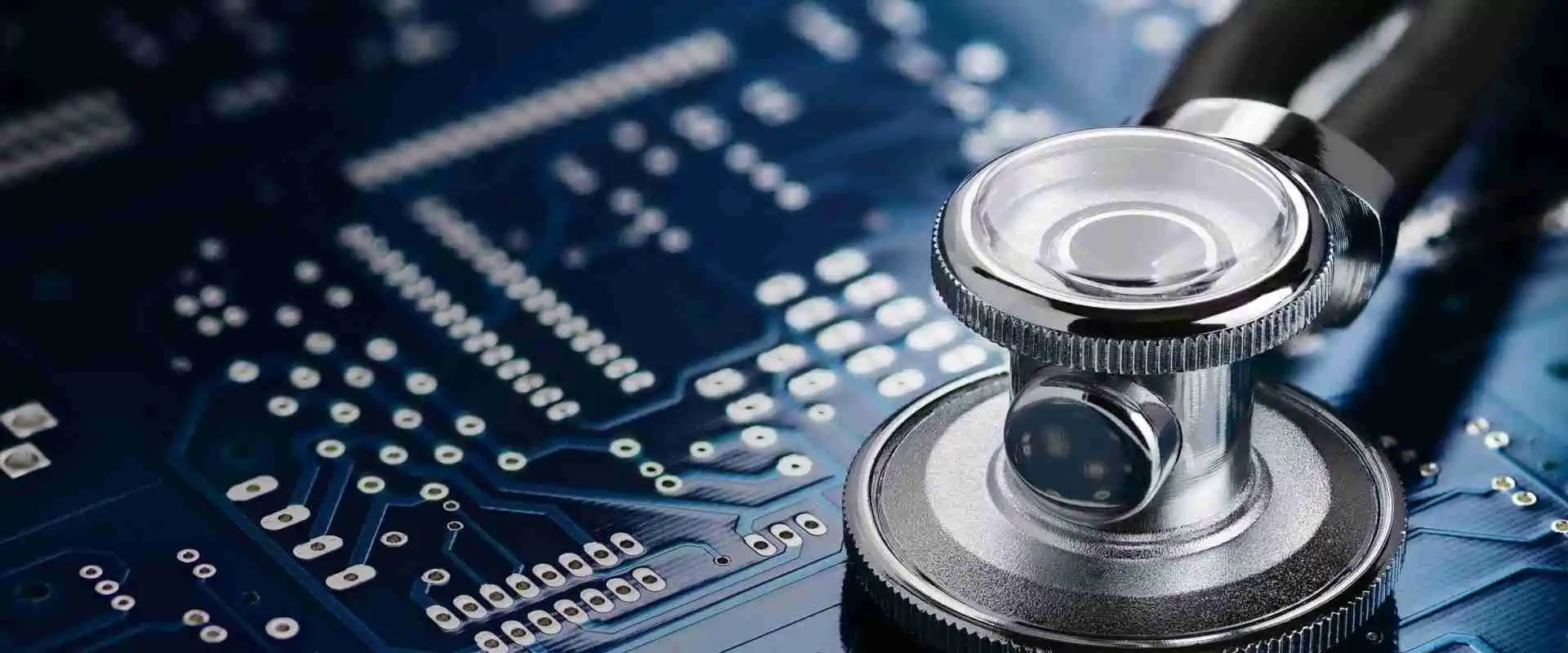
Special considerations must be made when designing electronics to be used in the medical and healthcare industry. Due to the fact that we are talking about human life, the quality and sustainability of these pieces of equipment is important.

Medical electronics manufacturing has become a popular term used to highlight the processes that go into the making of these devices. In this article, we will help you understand what the manufacturing process looks like. You will also find out some of the devices that can be made with these processes.

What are Medical Electronics?

An apt description is that these are the devices or pieces of equipment exclusively used in the medical sector. From the implantable medical devices to the monitoring systems; there are lots of medical electronic devices you can find out there.

These are also the devices used for facilitating different medical treatment options. Hence, producing them the right way is a must. Most times, the medical electronics companies are hired for the job and allowed to control most parts of the process โ€“ including component sourcing.

Factors Fueling the Demand for Medical Devices Electronics

Medical Devices PCBA

Several factors are responsible for the massive demands for medical electronics manufacturing services, whether as a one-off project or an ongoing working relationship.

Improved Life Quality

These devices are used for one major goal โ€“ to improve the quality of life (of the patients). Thus, it is expected that the medical electronics will meet the requirements of excellent diagnose and bolstering of the treatment options.

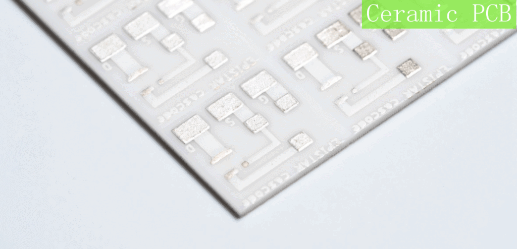
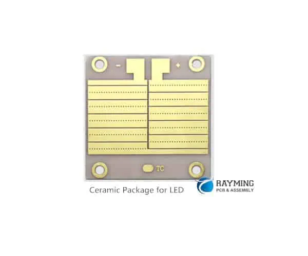
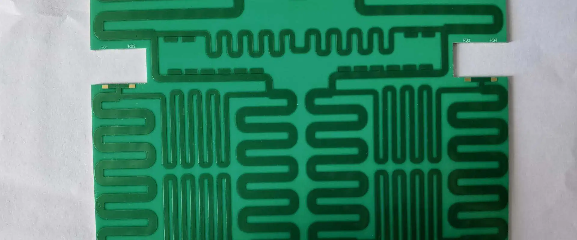
High-Quality PCB Selection
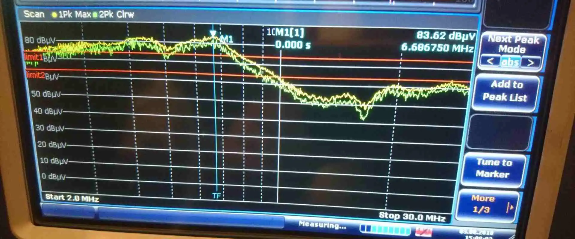
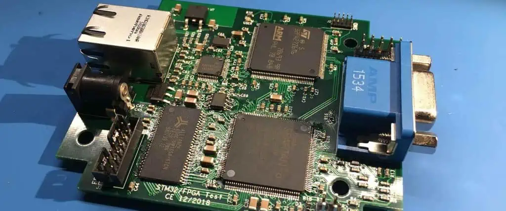
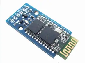
A bulk of the medical equipmentโ€™s functionality lies with the quality of the circuit board used therein. Hence, the priority is on choosing an OEM medical electronics manufacturing company that uses high-quality and high-performance Printed Circuit Boards (PCBs).

An Emphasis on Quality Standards

There is an emphasis on the medical electronic devices that meet the desired standards. It is expedient to mention that these standards are in line with the laid-down guidelines by the Food and Drug Administration (FDA), as well as other concerned health-related agencies.

These emphases help the manufacturer to design and manufacture the pieces of medical equipment to meet the strict regulations and standards.

Medical Electronics Design and Manufacturing Processes

If there is one major concern as to how medical devices are to be manufactured, it is usually based on the processes. There are two major processes, which are the traditional method and the additive manufacturing process.

It is noteworthy that both of these processes are unique and offer some considerable advantages over the other.

With that being said, let us quickly look at some of the differences between the traditional and additive medical electronics manufacturing processes.

Traditional vs. Additive Medical Electronics Manufacturing Processes

Traditional manufacturing processes refer to the common methods or pathways used to manufacture medical electronic devices. The popular ones are Injection Molding and CNC Machining. The traditional process is also ideal if you are working on higher volumes of these devices, as it helps to scale the process, cut down on lead time for tooling and saves costs.

On the other hand, you can use the additive medical electronics manufacturing process to make medical devices that are limited. In this instance, you are working on a low volume. You will also find the additive manufacturing process suitable if you are making either the proof-of-concept designs or prototypes of those devices.

1. Types of Traditional Medical Electronics Manufacturing Processes

FULL PCB MANUFACTURING Quote

Let us look at some of the processes or methods that can be used to manufacture medical devices โ€“ the traditional way.

Injection Molding

This type of traditional medical electronics production process is ideally used for the higher-volume medical devices. We are looking at the likes of:

  • Beakers
  • Laboratory equipment housings/casings
  • Containers
  • Plastic surgical components
  • Test tubes and;
  • Syringes

For the best results, a wide range of materials are required to attain the reliability of these devices. Examples of the features of the materials required for the process include but are not limited to:

  • Flexibility: these materials are required to be highly-flexible. An example of such is silicon plastic.
  • Medical-Grade: this is required mostly for making the biomedical implants.
  • The materials are required to have a combination of higher durability and strength, especially for the plastics.
  • Sterilizable: this property or feature is required when manufacturing specific medical devices, such as dental and surgical tools.

The advantages of the Injection Molding medical electronics manufacturing process include:

  • It supports a wider range of thermoplastic polymer colors and materials.
  • It is not only suitable for complex geometries. It also offers higher dimensional accuracies.
  • Shorter Lead Time: it has a shorter production time, which takes anywhere between 15 and 60 seconds per component, after the initial start-up.
  • There is a higher level of consistency and repeatability of the componentโ€™s finishing process and the geometry.

Some of the reasons why you may not want to use the Injection Molding process include the limitation of the component materials to the thermoplastic polymers. You will also spend a lot of money to make custom medical pieces of equipment, as well as paying more to manufacture the mold.

CNC Machining

This traditional medical electronics manufacturing process is best if you are working with the higher-volume products, which also double as the final designs of the devices.

The best parts or attributes of the CNC Machining process are:

  • The CNC machines have applications that are suitable for most part materials and geometries.
  • The machines also cover a wide range of machining processes and cutting tools.

For the best results, be picky about the componentโ€™s material and geometry, as those two factors potentially influence how the devicesโ€™ performance will be like.

The benefits of the CNC Machining process for electronic devices include:

  • It offers a combination of automated process, which, in turn, encourages continuous operations.
  • Higher dimensional accuracy is attained in the process.
  • The CNC Machining process also supports a wide range of materials, as well as complex part geometries.

On the flip side, the process takes longer to complete and this is due to the individualized CNC programming of the parts. You will also spend a lot of money to make a CNC programming of each part and initial training.

Additive Manufacturing Process for Medical Electronic Devices

The additive manufacturing process is your go-to when making prototypes of the electronic devices, as well as producing a limited number of these devices.

The following are some of the processes that can be used:

Metal Printing

This additive manufacturing process has an extensive application or use case than some of the others we will discuss in this article. The extensive usage is mainly because of the printing capability for the complex geometrical shapes.

Other factors that bolster the extensive applications are:

  • The compatibility of the materials with biomedical implants.
  • Higher material properties
  • The sterilizability for the surgical tools.

Generally, the Metal Printing additive manufacturing process is ideal for complex medical electronic designs that require improved material strength.

Here are some of the best attributes:

  • It supports a wide range of materials, including the superalloys and metals.
  • It supports the production of complex and bespoke components with the geometries that the traditional manufacturing processes donโ€™t support.
  • Metal Printing enables the miniaturization of componentsโ€™ weight, as well as the topological optimization of the same.

On the downside, you wouldnโ€™t be able to make something out of the existing designs, especially if you are looking at making 3D prints. Also, the associated costs of making 3D metal prints are higher.

Fused Deposition Modeling

medical pcb assembly

Abbreviated to FDM, this is an additive medical electronics manufacturing process that is ideal for the simple geometries. You also want to use it if you are working within a constrained budget.

For the best results, consider using the Fused Deposition Modeling (FDM) process when making medical devices that donโ€™t require much medical strength.

Here are some of its benefits:

  • The availability of several plastic materials, especially those that are sterilizable for surgical devices and compatible with biomedical implants.
  • The varieties of available materials are usable for different purposes, such as non-commercial function applications and making prototypes of specific medical electronic devices.
  • The affordability makes it easier to produce custom thermoplastic parts and making prototypes of the same.

Selective Laser Sintering

Also called the SLS process, Selective Laser Sintering refers to the production pathway for specific medical electronic tools, such as dental and surgical tools.

You want to also consider using it for the following reasons:

  • It makes the small and medium batch productions of medical electronics easier.
  • The SLS parts have distinct attributes, such as excellent strength and a higher level of accuracy. The isotropic mechanical properties also make them ideal for the prototypes and the functional parts.
  • The streamlined design process is not complicated, hence, bolstering the speed at which the complex geometries can be produced.

Despite these upsides, there are a couple of negativities about the Selective Laser Sintering (SLS) process for additive manufacturing. These disadvantages include:

  • It is almost impossible to make the prints on the small holes and large, flat surfaces. This is because of the fact that such could expose the holes and surfaces to over-sintering and warping.
  • Owing to the popularity and availability, it takes a long (lead) time to have the 3D prints of the medical devices readied.

Stereolithography

With the short form as SLA, Stereolithography refers to the 3D printing technology used for attaining higher levels of aesthetics and details for medical devices.

The attributes include but are not limited to:

  • Specialized materials, such as flexible and castable resins are used for the design.
  • You can count on the Stereolithography process to support the production of medical electronics with intricate details and higher dimensional accuracies.
  • It is the ideal medical electronics manufacturing process for devices that donโ€™t require higher material strength and which lower-cost prototypes.
  • The Stereolithography (SLA) process is to be used for making visual prototypes of medical devices and this id due to the very smooth surface finish.

On the flip side, you need to have second thoughts about the process due to the following reasons:

  • Visual marks are usually left behind. This often requires post-processing to get rid of the visual marks left behind on the SLA component.
  • It is not always possible to use the SLS parts for the functional prototypes of medical devices and this is because these parts are brittle.

Categorization of the Medical Electronics Manufacturing Devices

Medical Devices pcb
Medical Devices pcb

There are three (3) major categories or classifications of the devices manufactured for the medical industry. These categories are based on the regulations set aside by the Food and Drug Administration (FDA) based on the risks of these medical devices.

Before we delve deeper, note that these categories are based on โ€œClassesโ€ and start from Class I to Class III. The next important point to note is that the medical devices that fall under Class I are considered low-risk, while those between Class II and Class III are considered medium-risk and high-risk, respectively.

1. Class I Medical Devices

Generally, these are the devices or pieces of equipment that donโ€™t find their ways into the theatres or surgical rooms. They are more of randomized devices used for other medical purposes, other than saving or sustaining lives.

Despite the limited usage for supporting life, the Class I medical devices are subjected to some checks to be sure of the accurate performance. They are evaluated along the lines of device registration, branding and possible exposure to adulteration.

2. Class II

These are the medium-risk medical devices. In addition to implementing general controls, the FDA also recommends a couple of other measures to standardize the use of the Class II medical devices. Some of these measures include:

  • Evaluating the deviceโ€™s performance.
  • Post-market surveillance and;
  • Special labeling requirements

3. Class II Medical Devices

These are the riskiest of the electronics for the medical industry โ€“ and should be well-regulated. They are primarily used for different life-saving medical procedures, including surgical operations.

Understanding the FDAโ€™s Regulations for the Medical Electronics Market

The Food and Drug Administration (FDA), has made a list of different regulatory policies in place to facilitate the regulation and confirmation of the performance of medical devices.

The following are some of the regulations in this regard:

1. Registration

This regulation requires any or all of the medical electronic companies, manufacturers and the initial distributors of the medical pieces of equipment and devices to get registered with the Food and Drug Administration (FDA).

This is mostly for the companies looking to offer these services in the United States.

2. Medical Device Listing

After the registration is completed and the manufacturers, and distributors have been registered, they now move to stage 2. Here, the manufacturers are required to list or register the medical electronics and devices they produce with the FDA.

3. Premarket Notification

The fact that a medical electronics manufacturer is registered with the FDA doesnโ€™t mean an expression permission to distribute the devices.

Depending on the risk level (Class/category) of the devices, these manufacturers might be required to hold-off the distribution until they send a premarket notification or approval from the FDA.

It is up to the FDA to determine if your medical devices are ideal for the market or not. If they are, you will get an acceptance letter, giving you the go-ahead to start the commercial distribution of the devices.

4. Premarket Approval

This has to do with the receipt of the acceptance letter by the FDA, permitting you to start commercial distribution of the medical devices. However, you must note that the clinical trial data and any other required documentations would be asked to help determine if the devices are fit for the market.

Besides the distribution of the devices, seeking premarket approval is also important before engaging in an active promotion and or marketing of these medical pieces of equipment.

5. Investigational Device Exemption

Based on the risk exposure (Class) of the medical devices, the FDA might want to subject these medical devices to clinical studies. This is done to gather relevant data that supports whether the devices are ideal for the market, which, in turn, facilitates the issuance of the letter of acceptance.

6. Quality System Regulation

This is the FDAโ€™s way of checking, confirming and overlooking the quality of the medical device contract manufacturerโ€™s internal processes for making those devices.

Some of the processes checked with the quality system include:

  • Design
  • Manufacturing process
  • Labeling
  • Packaging
  • Storage
  • Purchase
  • Installation and;
  • Servicing of the medical devices

For the best quality assessments, the FDA uses a framework, which aids in the evaluation of the different requirements and specifications that make the medical devices reliable.

7. Labeling

The labeling requirements specify the type of information to add in the labels of medical devices. It also has to do with the following:

  • The position for applying the labels, including a direct application on the device.
  • It specifies whether the information is to be added to the packaging.
  • Label requirements also specify the type of options, such as manuals or any other supported form of literature.

8. Medical Device Reporting

With the medical electronic devices readied, approved and pushed into the market, there is another task for the manufacturers. As per the 21 CFR Part 803 of the Title 1 US Code of Federal Regulations (CFR) Code 800, there is a provision for medical device reporting.

It specifies that the medical device manufacturers must report incidences arising from the use of those devices. These reports cut across malfunctioning devices and exposure to incidents that led to death or bodily injury to the users.

How to Get the Best Electronic Manufacturing Services for Medical Devices

Several factors are worth considering to help you make an informed decision on the best ways to get started with medical electronics manufacturing.

The following tips should point you in the right direction:

1. Choose the Best Medical Device Contract Manufacturer

With several medical device contract manufacturing companies, you can be sure to have a lot of options to choose from.

However, you should prioritize the most important factors, such as:

  • Make sure that the Contract Manufacturer (CM) is registered with the Food and Drug Administration (FDA). Also, find out whether the CM is permitted to manufacture the type of medical device you want.
  • What is the manufacturerโ€™s throughput? This is directly proportional to the types of equipment it uses, the manufacturing process and the number of employees on ground to facilitate the project.

2. Tailored Medical Device Manufacturing Solutions

Your medical device contract manufacturer should incorporate design considerations to bolster the production process. This also includes having an eye for details towards the implementation of the Design for Manufacturing (DFM) guidelines.

3. Risk Management

How effective is the CM in managing the risks arising from manufacturing medical devices? In addition to having the ISO 14971, the manufacturer should also exert the capabilities to trace and fix design errors as soon as possible.

4. Supply Chain Integrity

The reliability of the medical devices is further improved with the traceability of the supply chain. The supply chain includes where the components/parts are sourced. It is important to purchase medical device components from the FDA-registered suppliers.

5. Agile Manufacturing Process

Having an agile manufacturing process for medical devices aids the Contract Manufacturer (CM)โ€™s capability of identify potential risks and have them fixed in real-time. The responsiveness of the manufacturer in this regard is a boost to the production process, as it helps to minimize the prevalence of gaps in the production process.

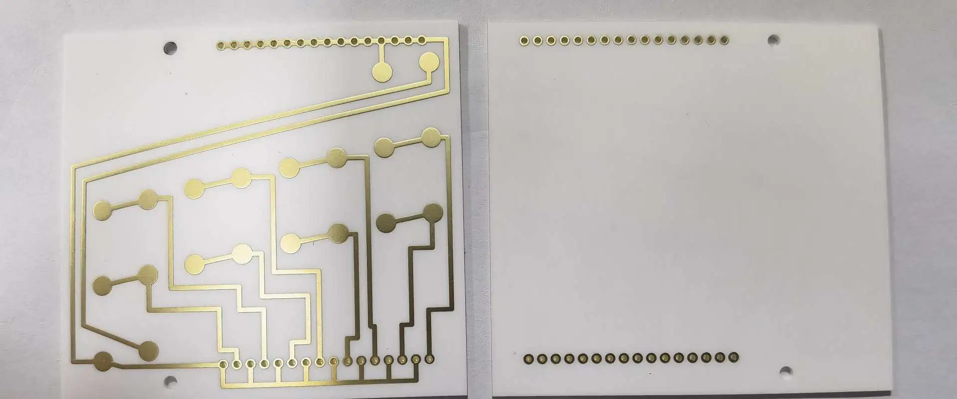
6. Circuit Board Design Transfer

As the Printed Circuit Board (PCB) forms a baseline for most medical devices, it is expedient to ensure the smooth transfer. Irrespective of the design process/schematic to the board for onward production, it must be smooth and done in accordance to the prevailing documentary controls/procedures.

Final Words: The Medical Device Market at a Glance

Medical devices and pieces of related equipment will continue to be in high demand, as we need to have the right facilities in place to cater to the ailing population. RAYPCB Technology, in a 2022 report, projected a $13.4 billion market valuation for the global medical electronics manufacturing market.

In the coming years, we will see fundamentals and trends like medical 3D printing, the high demand for ventilators, sensors and wireless technologies, as well as an increased adoption of telemedicine influencing the growth of the market.

As these changes are bound to come, you want to secure your spot and manufacture the best medical devices that align with the new trends. Reach to a reliable Contract Manufacturer (CM) today for a quotation!

Guide to EMI Issues in PCB: Electromagnetic Issues

EMI Issue

PCB designers frequently confront electromagnetic challenges, necessitating system design engineers to monitor electromagnetic interference and compatibility continuously. Regrettably, minor design issues may lead to electromagnetic complications, which are more prevalent than ever as board designs shrink and customers request higher speeds.

There are two main concerns: 

Electromagnetic compatibility (EMC) and electromagnetic interference (EMI). EMC relates to the creation, transmission, and reception of electromagnetic energy, often caused by inadequate design. EMI, on the other hand, refers to the harmful and unwanted impacts of EMC and interference from external electromagnetic sources. Excessive EMI can cause defects or damage to the product. To mitigate the effects of EMI, PCB designers must adhere to EMC design guidelines.

EMI in circuit boards can be reduced through proper EMC design, which is fortunate.

YouTube video

Types ofย EMI Issues in PCB

EMI problem
EMI problem

You can categorize EMI into two types:

  • ยท Broad EMI
  • ยท Narrowband EMI

One can generate Narrowband EMI within a limited range of frequencies, sometimes even just one frequency. Radios, cell phones, and TV stations are familiar sources of this type of EMI, which can occur intermittently and continuously. While disruptive, narrowband EMI typically does not cause equipment damage, but broadband EMI does. Broadband EMI is more widespread and can cause harm to electronic devices. Various sources, such as a motor, Faulty fluorescent lamps, car ignition, Faulty electrical lines, and the jet engine, can cause it. Broadband EMI interferes with the intended signals of electronic devices.

EMI that occurs over a wide range of frequencies is often caused by radio frequencies, the most frequent source. Lightning, power lines, circuits, lamps, and other sources can emit energy that produces this type of interference.

When electronic devices fail to function correctly, it can indicate this type of EMI. In a household setting, it may only cause minor interference with electronics, but it can potentially cause hardware damage, data loss, and reduced productivity in industrial sectors.

Sources of EMI

Sources that can produce EMI include:

ยท Natural sources of EMI

Natural sources, like lightning strikes, static, cosmic noise, solar flares and dust, atmospheric electricity, and snowstorms, & the sun, can cause this kind of EMI.

If not adequately protected, this EMI suddenly impacts electrical devices, including military equipment and transportation systems. Weaker forms of EMI, like that created by snowstorms, can Interrupt phone signals.

ยท Residential EMI

Wireless devices and electronic appliances are also familiar sources of this EMI. Although this kind of EMI typically does not cause permanent loss, it can still disrupt and impair the functioning of other electronic devices.

Wi-Fi devices, laptops, cell phones, microwaves, Bluetooth devices, baby monitors, toaster ovens, and many other electronic devices can cause residential EMI. As we add Extra electronic Gadgets to our homes, we increase the number of potential EMI sources.

The electronic’s quality can also affect artificial EMI. Electronics with higher performance levels and operating frequencies may have a greater risk of producing EMI.

ยท Industrial

This form of EMI is generated on a larger scale or can result in significant interference. Sources of this kind of EMI are diverse. They can include electric motors and generators, telephone and cellular networks, satellite transmissions, radio and television, railroads, power grids, medical equipment, and many others.

The Significance of EMI Shielding in PCB Industry

It is crucial for safeguarding sensitive electronic layouts from interference and preventing More powerful signals from disrupting nearby electronics. A printed circuit board design checklist can assist in remembering which components require protection and how to do so effectively.

EMI can impact sensitive electronics across various sectors, ranging from personal to industrial electronics, as well as emergency systems and critical military. Therefore, it is vital to take every possible measure to shield electrical systems against EMI.

What are EMI Issues in PCB, Shielding and How Does it Work? 

FULL PCB MANUFACTURING Quote

EMI shielding involves covering circuits with shields that safeguard them from radiation & electromagnetic signals absorption that could cause EMI.

EMI shields attenuate the interference and generate a current flow in the shield’s metal. It is then directed toward the ground reference plane.

EMI Shielding in PCBs 

Shielding in Printed circuit boards is employed in various applications such as medical, military, and communication. It is frequently implemented in the steps most susceptible to EMI, including the output, input, and amplifier.

To prevent typical circuit board issues, it is essential to shield them with some metal shields, which can safeguard them from radiation and EMI absorption. The circuit and components are isolatable from other boards to achieve this.

EMI Issues In PCB: Design Principles 

To reduce EMI, PCB designers must adhere to electromagnetic compatibility layout principles. The primary reasons for EMC issues typically stem from design defects that lead to interference between traces, PCB coils, vias, circuits, and other components. Incorporating these crucial design fundamentals can aid in preventing and addressing electromagnetic issues in the PCB design.

1. Ground Plane

Creating a ground plane for a PCB is an essential and crucial step in minimizing electromagnetic interference (EMI). The ground plane is the primary protection against EMI because all circuits need a ground to function correctly. To reduce EMI, there are several recommended effective practices for designing the environment, such as:

  • Maximize ground area: To minimize emissions, noise, and cross-talk, it is recommended to maximize the ground space in the Printed circuit board by increasing it as much as possible. It allows signals to disperse more simply, resulting in better performance. If the ground plane is insufficient, one possible solution is to add an extra layer or generate a multi-layer Printed circuit board. It offers more flexibility in handling high-frequency traces.
  • Use solid planes: Solid ground planes are highly recommended, particularly for a multi-layer printed circuit board. The Copper-thieving or etched ground planes tend to have higher resistance levels, whereas unbroken ground planes offer lower impedance levels.
  • Connect each component: It is advisable to connect every element to the ground plane and point to ensure the ground reference plane is a buffering agent for a circuit board design. Floating components are unable to utilize the benefits of the ground plane fully.
  • Split planes: Complex PCB designs frequently require multiple regulated voltages, each requiring its ground plane. However, incorporating many ground reference planes can raise fabrication costs. To address this issue, split planes can be useful. It allows multiple ground parts to be creatable on a single layer. Designers should use partitioned planes judiciously, though, and only when necessary. When implementing split planes, it is crucial to connect them at a single point to avoid creating loops. It which can result in the antenna that emits EMI.
  • Connect bypass: When bypass and decoupling capacitors are part of the design, it is vital to join them to a ground plane. Doing so helps to reduce the loop size, lessening the ground current.
  • Signal length: Trace length is a critical factor as the time taken by a signal to travel to or from its source needs to be consistent. Otherwise, it causes EMI radiation. To minimize this, we recommended keeping trace(routing) lengths short and ensuring that they are roughly the same in size.

2. Trace Layout

PCB Design Guidelines For EMI EMC

Traces are crucial in board design as they propagate the current correctly. However, If the paths are not ordered following top EMC layout rules, numerous issues can arise.

Traces are conductive pathways that carry flowing electrons when the circuit is active. Consequently, a single mistake in their design can transform them into radiating antennas. Even something as simple as a bend or a cross in a trace can lead to Printed circuit board electromagnetic interference.

Here are some recommended rules for route layout in printed circuit board design:

  • Avoid right angles: It is advisable to avoid angles between 45 and 90 degrees for traces, vias, or additional parts in Printed circuit board design. Capacitance tends to increase as paths exceed 45-degree angles. It causes a change in characteristic impedance and subsequent reflection. Reflection can lead to EMI. To prevent this, traces that have to take a turn around a corner should be rounded or routed through 2 or more turns at an angle of 45 degrees or less.
  • Keep signals separate: To prevent interference, we recommend maintaining fast-moving signal paths away from slow-moving ones. Also, keep analog signals away from digital signals. The proximity between these signals can cause interference.
  • Shorten return paths: To minimize interference, it is crucial to keep the way of the current returning shortly and trace them along the traces of minimum resistance. We recommend that the return paths be roughly the same length as the transmit traces and even shorter.
  • Mind spacing: When Dual high-speed signals run parallel to each other, they can create electromagnetic interference (EMI) through a phenomenon known as cross-talk. So here, one of the traces is referred to as the “aggressor,” while the other is a “victim.” Additionally, the aggressor trace affects the victim trace by inducing and coupling capacitance and inductance, generating both backward and forward currents in the victim trace.

To reduce cross-talk, it is recommended to maintain a minimum distance between traces. Typically, the separation should be at least twice the width of the path. For instance, if the path is 5 mils wide, ensure The least distance of 10 mils or more among 2 parallel traces.

  • Use vias carefully: PCB designers use vias to take benefits of different layers in their boards when tracing. However, vias should be useful cautiously as they put in their capacitance and inductance effects. It can cause bouncing back of signals because of signal strength alterations. Vias make the trace longer, which must be balanced. Differential traces should not be routed through Vias if possible. If unavoidable, use vias in both conductive paths to regulate the delay.

3. Component Arrangement

Proper arrangement of electronic components is crucial to prevent EMI issues in an electronic circuit. While designing a Printed circuit board, it is vital to consider the EMI impact of each part. Some of the effective practices for element layout in Printed circuit board design are as follows:

  • Separate analog & digital parts: To prevent cross-talk and other issues, it is essential to keep digital and analog circuits or components separate in PCB design, similar to trace separation. Placing them in close adjacency can cause interference. To avoid this, designers can use multiple layers, shielding, and Individual grounds to keep digital and analog signals apart. We often recommend keeping them on utterly separate ground planes.
  • Separate analog & high-speed pieces:  Analog circuits typically carry high electric current. It can cause issues for high-frequency traces or switching signals. It’s essential to keep these circuits separate from each other and use ground signals to shield analog circuits. On Multi-layered PCBs, we recommend route analog traces to create a ground reference plane between an analog circuit board and the high-frequency signals.
  • High-speed components: The smaller and faster the electronic component, the higher the chance it will produce a considerable amount of EMI. To counteract this, we recommend implementing shielding or filtering techniques. Additionally, it’s essential to Divide these elements from other elements in the board design. Another strategy is to have as high-frequency signals & clocks as possible adjacent to a ground plane, which helps to minimize cross-talk, radiation levels, and noise, keeping them within acceptable limits. 

4. EMI Shielding

Regardless of the design rules you adhere to, specific components will inevitably generate electromagnetic interference (EMI), tiny and high-speed Units. However, the effects of this EMI are reducable by shielding and filtering. There are various shielding and filtering techniques available, some of which are:

  • Component and board shielding: Metallic packages known as physical protection one can use to enclose all or a portion of a circuit board. Their primary purpose is to prevent electromagnetic interference (EMI) from infiltrating The board’s electrical connections, and the methods used to achieve this goal differ depending on the source of the EMI. When EMI arises from the system, element/component shields can encapsulate a particular component that generates EMI.

This ground connection reduces the size of the antenna loop and absorbs the EMI. To safeguard against external EMI sources, other types of shields can cover the entire circuit board. A Faraday Cage is an example of a thick protective enclosure that obstructs RF waves. Typically it has metal and conductive foam, these shields are useful for this purpose.

  • Low-pass filtering: In some instances, a printed circuit board can incorporate high-cut filters to eradicate high-speed noise that emanates from elements. These filters stifle the noise from 3 parts, permitting the electric current to flow unobstructed On the way back.
  • Cable shielding: EMI issues are most prominent in cables that transport both analog & digital currents. These cables generate parasitic capacitance & inductance, particularly for high-speed signals. However, insulating these cables and grounding them at both ends can eliminate EMI interference.

Conclusion

Electronics can experience significant malfunctions due to EMI. Hence, when creating a printed circuit board, it is essential to carefully consider which shielding method is most suitable to guarantee the system’s optimal performance.

Everything You Need to Know About 1050C Ceramic Board

1050c ceramic board

A ceramic fiber circuit board is a firm item produced from various ceramic fiber aggregates, possessing remarkable chemical stability. It is created using wet method organic bonding & vacuum forming techniques, making it suitable for multiple industries.

A high-temperature thermal insulation element known as a 1050C ceramic board can endure temperatures as high as 1050ยฐC. Moreover, this ceramic board is usually crafted from compressed alumina-silica & refractory fibers joined together, implementing a binder element to produce the rigid board.

In high-temperature applications that necessitate thermal insulation and resistance to thermal shock, 1050C ceramic circuit boards are frequently employed. So these boards are typically utilized in kilns, industrial furnaces, and other equipment as they offer outstanding insulation and contribute to energy conservation. Additionally, they are impervious to chemical corrosion or can endure exposure to severe surroundings.

A broad assortment of grades, densities, or hardness levels is utilized in their manufacturing.

Characteristics of 1050C Ceramic Board

  • Exceptional pressure endurance and extended lifespan.
  • Minimal thermal storage capability and conductivity.
  • Material with high flexibility and toughness, not brittle.
  • Precision high dimensions & superior flatness.
  • Simple to cut and convenient for installation.
  • Exceptional resistance to corrosion caused by wind.
  • Uninterrupted production, uniformly dispersed fibers, and outstanding stability.

Applications of 1050C Ceramic Board:

  • A heat-insulating material for the furnace back lining utilized in the cement & building materials industries.
  • A heat-insulating material for the furnace back lining utilized in the petrochemical, ceramic, ceramic, and glass industries.
  • A heat-insulating material for the furnace back lining utilized in temperature treatment processes.
  • Besides, a heat-insulating material for the furnace back lining is utilized in the non-ferrous metal industries.
  • Moreover, a heat-insulating material for the furnace back lining is utilized in high-temperature response or heating equipment.

To cater to various applications, 1050C ceramic circuit boards are produced in a diverse range of sizes & thicknesses. Their lightness allows for hassle-free handling and installation, and their flexibility enables easy cutting and shaping to accommodate intricate geometries, rendering them appropriate for an extensive array of applications.

An essential advantage of 1050C circuit boards is their exceptional insulation capacity. Additionally, with their poor thermal conductivity, they can minimize heat loss or enhance energy efficiency. Furthermore, their extensive heat capacity enables them to slowly store or release heat, contributing to stabilizing the temperature within the equipment.

An added benefit of 1050C circuit boards is their ability to resist thermal shock. So they can endure abrupt temperature alterations without fracturing or shattering, thereby rendering them ideal for Applying in tools that undergo rapid temperature fluctuations. Furthermore, they are resistant to corrosion and can bear exposure to severe surroundings, making them a preferred option in fields like metallurgy, chemical processing, and glass production.

Major Uses of 1050C Ceramic Board

FULL PCB MANUFACTURING Quote

Below are several general applications of 1050C ceramic circuit boards in different industries, categorized by headings:

Industrial Furnaces and Kilns

1050C ceramic circuit boards find widespread use in industrial kilns and furnaces as insulation, where they lower heat loss and improve energy efficiency, resulting in cost savings over time. Their ability to endure high temperatures & and thermal shock renders them well-suited for these purposes.

Automotive Industry

The automotive sector employs 1050C ceramic circuit boards in exhaust systems for insulation purposes and to minimize heat transfer. So these boards can endure high temperatures or chemical corrosion, rendering them optimal for this use case.

Glass Manufacturing

The glass manufacturing industry utilizes 1050C ceramic circuit boards for insulation purposes and to protect their tools from thermal shock. These boards can withstand sudden changes in temperature and high temperatures, making them an appropriate choice for this industry.

Chemical Processing

1050C ceramic circuit boards are commonly utilized In chemical manufacturing to provide thermal insulation or protect tools from deterioration. Their ability to Withstand contact with harsh chemicals & high temperatures makes them well-suited for this application.

Aerospace Industry

1050C ceramic circuit boards find applications in the aerospace industry, where they are used in engine Elements to Supply insulation or Decrease heat transfer. Additionally, due to their ability to withstand high temperatures & thermal shock, they are an ideal choice For the industry.

1050C ceramic circuit boards have a wide range of applications in different industries, including but not limited to industrial furnaces or kilns, chemical processing, glass manufacturing, automotive industry, and aerospace industry. They are valued for their excellent insulation properties, thermal resistance or chemical corrosion, and ability to withstand high temperatures, making them versatile and dependable materials.

Benefits of 1050C Ceramic Board

Ceramic Package for LED

There are several advantages of using 1050C ceramic circuit boards, which make them the favored option in different industries. Below are some of the benefits of 1050C ceramic circuit boards, along with their headings:

a. Thermal Insulation

1050C ceramic circuit boards benefit from Excellent Thermal Insulation, as they help reduce heat loss or improve energy efficiency. With low conductivity (thermal) & high-temperature capacity, these boards can store and release heat slowly, Preserving a stable temperature Interior of the equipment.

b. Resistance to Thermal Shock

1050C ceramic circuit boards are resistant to thermal shock, which means they can withstand sudden Modifications in temperature Beyond breaking or cracking. So this property makes them excellent for use in tools subjected to rapid temperature changes. Additionally, they can withstand high temperatures for long periods, making them a reliable and durable material for various high-temperature applications.

c. Chemical Resistance

The resistance of 1050C ceramic circuit boards to corrosion makes them appropriate for use in Extreme environments. So they can endure exposure to corrosive chemicals, such as acids and alkalis.

d. Lightweight and Easy to Handle

The lightweight nature of 1050C ceramic circuit boards makes them Simple to handle and install. So, their flexibility allows them to be shaped and cut to suit complex geometries, creating them a suitable material for various applications.

e. Versatile

Due to their versatility, 1050C ceramic circuit boards find various uses in various industries, such as industrial furnaces or kilns, chemical processing, glass manufacturing, the automotive industry, the aerospace industry, and more.

f. Cost-Effective

The use of 1050C ceramic circuit boards can lead to energy savings, which can result in cost savings over time. Additionally, they are durable and have a long lifespan, reducing the frequency of replacements & repairs needed.

To summarize, 1050C ceramic circuit boards are an excellent option for high-heat insulation purposes that demand thermal insulation, thermal shock resistance, and chemical resistance. Their adaptability, user-friendliness, and energy-saving characteristics make them a favored choice in diverse industries.

What Do You Need To Know About 1800 Ceramic Fiberboard?

1800 ceramic fiber board

A ceramic fiber circuit board is a refractory material made from alumina-silica fibers that are lightweight and suitable for use at the heat of 1430C. It is designed for thermal applications that require high rigidity, and its abrasion resistance and thermal insulation properties have been enhanced by increasing its density.

Ceramic fiber circuit board is a product formed under vacuum, which can withstand Increased gas speeds than Ceramic insulation blankets. Due to low conductivity and heat storage, it is well-suited for use in furnaces, boiler ducts, and stack lining applications. Its properties allow for shorter Manufacturing cycles and easier maintenance access in industrial furnaces.

The 1800 Degree Temperature Ceramic Board is an insulation material that can endure temperatures as high as 1800ยฐC. It usually comprises alumina-silica fibers/zirconia-silica fibers, which are each other by a binder material, creating a sturdy board.

The high-temperature ceramic fiber board withstanding up to 1800 degrees Celsius, exhibits outstanding thermal insulation properties, making it a perfect fit for high-temperature appliances that require heat loss reduction. Its minimum thermal conductivity characterizes its ability to minimize heat transfer, thus enhancing energy efficiency.

The 1800ยฐ High-Temperature Fiber Circuit Board is a lightweight and easily manageable option ideal for applications where Quantity is a crucial factor. Its flexibility allows it to be shaped and cut to fit complex geometries, making it a versatile choice for various applications. Furthermore, it is resistant to chemical corrosion and thermal shock, making it a durable or Durable insulation material. The board can endure sudden temperature fluctuations breaking and without cracking. It can withstand exposure to Hazardous chemicals and corrosive materials.

A high-temperature fiber circuit board finds widespread usage in industrial kilns, furnaces, and high-temperature equipment. It is also commonly use in industries such as aerospace, glass manufacturing, and automotive. It is primarily due to its remarkable thermal insulation properties, ability to withstand chemical corrosion and thermal shock, and its versatile nature and lightweight. These features make it a highly favored material across various applications.

Features of 1800 ceramic fiberboard

0.635mm Alumina Ceramic PCB
  • Sleek Surface.
  • Medium thickness and density.
  • Exceptional mechanical or structural strength.
  • The thermal conductivity is low, and the shrinkage is minimal, making it extremely lightweight.

Characteristics of 1800 ceramic fiberboard

The insulation material of the 1800ยฐ High-Temperature Fiber Board possesses various characteristics that make it a perfect fit for high-temperature Implementations. Some of its prominent features are as follows:

1. High-Temperature Resistance

With the ability to endure temperatures as high as 1800ยฐ, this insulation material suits for utilization in high-temperature Implementations.

2. Excellent Thermal Insulation Properties

Featuring minimum thermal conductivity, the 1800ยฐ High-Temperature Fiber Board can decrease heat transfer, thus increasing energy efficiency. Additionally, it exhibits High thermal capacity, enabling it to retain and Discharge heat gradually. As a result, it aids in sustaining a consistent temperature within the equipment.

3. Resistance to Thermal Shock

Due to its ability to withstand sudden temperature fluctuations without developing cracks or fractures, this insulation material is suits application in tools that experience fast temperature changes.

4. Resistance to Chemical Corrosion

The 1800ยฐ High-Temperature Fiber Board possesses Opposition to chemical corrosion, rendering it an appropriate option for utilization in Severe environments. It can endure exposure to Toxic chemicals, such as alkalis, acids, and other corrosive agents.

5. Lightweight and Easy to Handle

The insulation substance is easily manageable and lightweight, facilitating effortless installation and handling. Its flexibility allows simple cutting and shaping to conform to intricate geometries, making it a versatile option for various applications.

6. Versatile

The 1800ยฐ High-Temperature Fiber Circuit Board is a versatile material that finds usage across a broad spectrum of applications. It is frequently useful in kilns and industrial furnaces, as well as in aerospace, automotive, glass manufacturing, chemical processing, and others.

In conclusion, the 1800ยฐ High-Temperature Fiber Board presents many features, such as high-temperature endurance and exceptional thermal insulation features. It also features resistance to shock & chemical corrosion, versatility, and a manageable structure. These attributes render it a dependable and widespread insulation material utilized across various industries and applications.

Applications of 1800 ceramic fiberboard

FULL PCB MANUFACTURING Quote

Below are some of the typical applications of the 1800ยฐ Temperature Fiber such as:

1. Industrial Furnaces and Kilns

Industrial kilns and furnaces often use the 1800ยฐ High-Temperature Fiber Board for insulation purposes, which helps to reduce heat loss. Thanks to its exceptional thermal insulation properties and low thermal conductivity, this insulation material is a perfect option for High-heat applications.

2. Aerospace Industry

The aerospace industry utilizes this insulation material to minimize heat transfer and provide insulation in engine equipment. Its widespread use is due to its lightweight nature, as well as its resistance to chemical corrosion and thermal shock.

3. Automotive Industry

The 1800ยฐ High-Temperature Fiber circuit Board is employed in silencer systems to Give insulation and minimize heat transfer. Its exceptional thermal insulation properties and ability to resist chemical corrosion make it an ideal material.

4. Glass Manufacturing

The glass manufacturing industry employs this insulation substance to give insulation and safeguard equipment against thermal shock. Its exceptional thermal insulation properties and capacity to resist sudden temperature changes and high temperatures render it an excellent material for Utilize in this sector.

5. Chemical Processing

In chemical processing, the 1800 Degree High-Temperature Ceramic Fiber Board supplies insulation. It also safeguards tools from Chemical erosion. Its ability to resist harsh chemicals, coupled with its exceptional Heat insulation properties, makes it a perfect material for this purpose.

Conclusion

The 1800ยฐ Temperature Fiber Board finds widespread use in different industries, such as kilns and industrial furnaces. You can also use it in chemical processing, glass manufacturing, automotive, and aerospace. Its reliability and popularity as an insulation material are due to its exceptional thermal insulation properties.

A Detailed Guide on 5050c ceramic board in PCB Industry

5050c ceramic board

A 5050C Ceramic Printed Circuit Board is a circuit board material made from ceramic, specifically designed for PCB fabrication. The ceramic material used in its production closely matches the Thermal expansion coefficient of copper, the commonly used material for printed circuit traces on the board.

Due to its outstanding thermal properties, the 5050C Ceramic PCB is an ideal material for high-temperature Tools. It can endure temperatures of 5050ยฐC and offers exceptional thermal conductivity, enabling efficient heat dissipation from delicate electronic components.

Additionally, the 5050C Ceramic printed circuit Board is resistant to chemical corrosion and thermal shock. It is making it a perfect Substance for use in severe environments that often involve exposure to high temperatures & corrosive chemicals.

Moreover, the 5050C Ceramic printed circuit board exhibits exceptional electrical insulation properties. Thereby, preventing electrical interference among various elements on the board. Furthermore, its high dielectric strength renders it a suitable material for high-voltage appliances.

The 5050C Ceramic printed circuit Board is a frequently used material in various electronic applications, such as high-temperature sensors, power electronics, and electronic control Components in the aerospace and automotive industries. Its popularity in these applications is due to its good thermal Characteristics, resistance to heat shock & chemical corrosion, as well as its outstanding electrical insulation Characteristics.

Features of 5050c ceramic board 

Ceramic PCB and Substrate

The 5050C Ceramic printed circuit Board possesses Various features that Create it a perfect element for electronic appliances requiring chemical resistance and high temperature. There are many noteworthy features such as: 

1. High-Temperature Resistance

The 5050C Ceramic Printed circuit Board can endure temperatures of 5050ยฐC, which makes it an excellent material for high-temperature appliances.

2. Excellent Thermal Conductivity

The 5050C Ceramic PCB Board provides exceptional thermal conductivity, enabling efficient heat dissipation from delicate electronic components.

3. Resistance to Thermal Shock

The 5050C Ceramic Printed circuit board exhibits high resistance to heat shock, rendering it a suitable material for use in severe environments where abrupt temperature variations occur frequently.

4. Chemical Resistance

The 5050C Ceramic PCB Board has excellent resistance to chemical corrosion. It is making it an ideal material for use in harsh environments where exposure to corrosive chemicals is common.

5. Electrical Insulation

The 5050C Ceramic Printed circuit Board possesses exceptional electrical insulation features that avoid electrical interference among the board’s various components. Additionally, it has great dielectric strength, which makes it an excellent choice for high-voltage appliances.

6. Lightweight and Durable

The 5050C Ceramic PCB is durable and lightweight, making it Simple to install and handle. Besides, it can Resist vibrations and physical stress, making it an ideal choice for electronic appliances that Demand durability.

The 5050C Ceramic Printed circuit Board boasts various beneficial features, including durability, High-temperature immunity, resistance to heat shock, good thermal conductivity & chemical corrosion, or electrical insulation. These components make it a top choice for electronic appliances that demand resistance to chemicals and high temperatures, such as electronic control modules, power electronics, and high-temperature Detectors in the aerospace and automotive industries.

Benefits & applications of 5050c ceramic board 

FULL PCB MANUFACTURING Quote

The 5050C Ceramic Printed circuit Board has several advantages and a diverse range of applications in different industries. There are many noteworthy applications and uses such as: 

Benefits:

ยท High-Temperature Resistance:

The 5050C Ceramic Printed circuit Board is highly resistant to high temperatures and does not degrade or break down, Building it a perfect fit for high-temperature appliances.

ยท Excellent Thermal Conductivity:

The 5050C Ceramic PCB Board exhibits outstanding thermal conductivity, facilitating efficient heat dissipation from delicate electronic parts.

ยท Chemical Resistance:

The 5050C Ceramic Printed circuit Board demonstrates exceptional corrosion resistance. Besides, this makes it an excellent option for deployment in severe environments where corrosive chemicals exposure is frequent.

ยท Electrical Insulation:

The 5050C Ceramic Printed circuit Board possesses exceptional electrical insulation properties that effectively Prohibit electrical interference among the various components mounted on the circuit board.

ยท Durable:

The 5050C Ceramic Printed circuit Board is durable and lightweight, enabling it to withstand physical stress & vibrations.

Applications:

There are many noteworthy applications such as: 

ยท Power Electronics:

The 5050C Ceramic Printed circuit Board finds utility in high-heat power electronics applications, including motor drives, inverter systems, or power supplies.

ยท High-Temperature Sensors:

The 5050C Ceramic PCB Board is employed in high-temperature detectors, such as thermocouples, that demand a substance with exceptional thermal conductivity and high-heat resistance.

ยท Aerospace Industry:

The aerospace industry deploys the 5050C Ceramic printed circuit Board in electronic control Components due to its exceptional durability and high-temperature resistance.

ยท Automotive Industry: 

The car industry leverages the 5050C Ceramic PCB Board in Electronic control units due to its impressive durability, high heat, and chemical resistance.

ยท Medical Devices:

The 5050C Ceramic Printed circuit Board finds use in medical Gadgets, including implantable devices and diagnostic equipment, that necessitate chemical and high-temperature resistance.

ยท Industrial Automation:

Ceramic Package for UV LED

 The 5050C Ceramic PCB Board is utilized in industrial applications, including control systems for fabrication processes, owing to its remarkable durability and high-heat resistance.

ยท LED Lighting:

The 5050C Ceramic Printed circuit Board is applied in LED(Light-emitting Diode) lighting appliances, such as high-power Light-emitting Diode drivers. It is because of its outstanding thermal conductivity and high-temperature resistance.

ยท Renewable Energy:

The 5050C Ceramic Printed circuit Board is implemented in Sustainable energy systems, including wind turbine generators and solar inverters, owing to its exceptional electrical insulation characteristics and high-heat resistance.

ยท Military and Defense:

The 5050C Ceramic Printed circuit Board is useful in military or defense applications, such as radar & missile systems. It is because of its remarkable durability and high-heat resistance.

ยท Semiconductor Manufacturing:

The 5050C Ceramic PCB Board is useful in semiconductor fabrication tools, including deposition and etching systems. It is because of its exceptional chemical and high heat resistance.

Conclusion

The 5050C Ceramic Printed circuit Board presents several advantages. It includes high-temperature resistance, remarkable thermal conductivity, electrical insulation, chemical resistance, and durability. Its extensive usage across diverse industries signifies its versatility and reliability as a material suited for high-heat electronic appliances that mandate resistance to chemical corrosion and thermal shock.

Everything You Need to Know About 3030C Ceramic Board

Ceramic PCB and Substrate

The 3030c printed circuit board is a ceramic substrate that finds application in electronic circuitry. Its ceramic composition boasts exceptional thermal conductivity & electrical insulation characteristics, rendering it a preferred material for high-performance heat dissipation in electronic devices.

The moniker “3030c” corresponds to its dimensions, typically measuring 30 millimeters on each side. Alumina, a high heat & corrosion-resistant chemical ceramic, is commonly used in production. These ceramic boards are prevalent in diverse electronic applications, including power electronics, Light Emitting Diode lighting & high-frequency equipment, owing to their ability to withstand elevated temperatures, exhibit exceptional thermal conductivity & offer superior insulation. In sum, ceramic circuit boards 3030c are integral components in numerous electronic equipment that demand optimal heat dissipation & top-notch performance.

The present article will examine various aspects of the ceramic printed circuit board 3030c and its characteristics, organized into distinct sections.

Features of 3030C Ceramic Board

Aluminum nitride ceramic circuit board

1. Material Composition

Constructed from alumina ceramic material, the ceramic circuit board 3030c showcases exceptional resistance to chemical corrosion and heat, owing to its high M.P. of roughly 2050ยฐC and excellent mechanical durability. Consequently, it represents an ideal substance for electronic appliances that demand efficient heat dissipation and high performance.

ยท Thermal Conductivity

With its excellent thermal conductivity, the ceramic circuit board 3030c can effectively dissipate heat from electronic equipment. Its thermal conductivity arises from the exceptional thermal conductivity of alumina material. Consequently, the ceramic circuit board 3030c is an optimal substance for electronic appliances that generate significant heat.

2. Electrical Insulation

Boasting exceptional electrical insulation, the ceramic circuit board 3030c can impede the current flow. Its electrical insulation characteristics stem from the high insulation resistance of alumina substances. As such, ceramic circuit board 3030c serves as an ideal substance for electronic appliances that demand elevated levels of insulation.

3. Size and Thickness

The ceramic circuit board 3030c comes in a standard size of 30mm square, making it suitable for various electronic applications. While its thickness may vary, it usually falls within the range of 0.5mm-1mm. Additionally, both the thickness & size of the ceramic circuit board 3030c can be tailored to meet the unique specifications of a particular electronic application.

4. Surface Finish

Although the texture of the ceramic circuit board 3030c may differ, it is usually smooth and level. It is a crucial factor as the surface finish can impact the operation of electronic equipment. An even and smooth surface finish guarantees the secure mounting of electronic devices onto the ceramic board and reliable contact between electronic equipment and the board.

Advantages of 3030C Ceramic Board

FULL PCB MANUFACTURING Quote

ยท High Thermal Conductivity

The ceramic circuit board 3030c is well-suited for applications where effective heat dissipation is essential, thanks to its superior thermal conductivity characteristics. Constructed primarily with alumina, a material known for its high heat transfer coefficient, this board facilitates heat transfer, enabling electronic devices to operate safely within temperature limits.

ยท Electrical Insulation

The outstanding electrical insulation properties of boards stem from the ceramic substance employed in the ceramic circuit board 3030c. This material is highly proficient at insulation, making it indispensable for high-voltage applications. By offering a dependable and secure solution for isolation, the board plays a critical role in numerous electronic appliances.

ยท High Strength and Durability

The strength & durability of ceramic substances is widely recognized. The ceramic circuit board 3030c, in particular, possesses a remarkable ability to withstand significant physical stress. This makes it a prime candidate for use in appliances where the circuit board is under mechanical pressure or vibration. Furthermore, this material is incredibly resistant to long-term wear, guaranteeing the board’s longevity.

ยท Corrosion Resistance

The chemical resistance of ceramic materials is well-established, and the ceramic circuit board 3030c is no different. It can endure exposure to a variety of chemicals & corrosive substances without sustaining any damage. As a result, the board is an excellent choice for use in challenging environments where exposure is a potential issue.

ยท Excellent Dimensional

The exceptional dimensional stability of ceramic materials is widely recognized, particularly in applications that require tight tolerances. The ceramic circuit board 3030c maintains its size and shape in high-temperature conditions. It ensures that electronic equipment functions in the specified parameters. This feature is critical in preserving the stability of the device and ensuring that it operates efficiently.

ยท High-Frequency Performance

The ceramic circuit board 3030c is exceptionally well-suited for high-speed electronic applications due to its outstanding high-frequency performance. The material’s(substance’s) high permittivity and low dissipation enable the circuit board to transmit high-speed signals without any loss or degradation. This feature is crucial for maintaining the integrity and quality of the signals, making the board an excellent choice for high-frequency applications.

ยท Low Cost

Ceramic materials are a cost-effective alternative to other substances like metal. With ceramic circuit board 3030c, electronic equipment manufacturers can create top-notch electronic devices at an affordable price without exceeding their budget.

Applications of 3030C Ceramic Board

ยท LED Lighting

LED lighting applications commonly utilize ceramic circuit boards 3030c due to their exceptional thermal conductivity characteristics. This feature allows for the effective dissipation of heat, which is critical for sustaining the performance and lifespan of LEDs. Moreover, the remarkable electrical insulation characteristics of the material ensure the safe function of the entire LED(Light Emitting Diode) lighting system.

ยท Power Electronics

To fulfill the demand for effective heat dissipation in power electronics appliances, ceramic circuit board 3030c stands out as a top choice due to its remarkable thermal conductivity characteristics. Furthermore, the board’s exceptional strength & durability render it perfect for deployment in high-stress power electronics appliances.

ยท High-Frequency Devices

Ceramic circuit board 3030c proves to be an excellent fit for high-speed electronic equipment, such as Radio Frequency amplifiers & microwave circuits, thanks to its remarkable high-frequency performance. Additionally, the substance’s low dielectric constant feature guarantees less signal degradation, resulting in high-resolution signal transmission.

ยท Automotive Electronics

The ceramic circuit board 3030c is well-suited for automotive electronics appliances due to its exceptional dimensional stability and high thermal conductivity. It can endure physical strain and high temperatures, rendering it a dependable solution for such applications.

ยท Aerospace and Defense

The demanding conditions and rigorous physical demands of aerospace & defense applications necessitate electronic components that can endure extreme environments. The ceramic circuit board 3030c, renowned for its exceptional strength, durability, resistance to corrosion, and outstanding electrical insulation qualities, is an optimal selection for such applications.

Conclusion

The ceramic circuit board 3030c finds extensive usage across various electronic appliances necessitating outstanding thermal dissipation, electrical insulation, durability, strength, and stability. Owing to its capability to withstand high-frequency signals and harsh environmental conditions, electronic equipment manufacturers consider it an optimal choice for their products.

To sum up, the ceramic circuit board 3030c presents many benefits that render it a perfect fit for electronic equipment manufacturers. Its superior thermal conductivity, outstanding electrical insulation, robust strength & durability, immunity to corrosion, exceptional dimensional stability, excellent high-frequency operation, and affordability combine to make it a favored option for various electronic applications.

The Essential Guide to Ground Loop PCB Techniques

PCB Ground Plane

Did you ever experience an annoying humming sound emanating from the sound system? Typically, the noise results from alternating current power(energy) lines entering the audio tool. When multiple pieces of equipment in a good design are linked to a common ground via different paths, a ground loop is formed. This loop makes a pathway for current to flow between various equipment grounds & back, ultimately resulting in humming caused by the current flow through an audio tool ground.

This article aims to examine the concept of the ground loop and provide insights into effective elimination methods.

YouTube video

The Need for Ground Loop PCB 

Circuits or Devices without grounding can lead to problems caused by significant static charges. In an ungrounded system, insulation leakage can cause the accumulation of substantial fixed amounts, posing a significant risk of electric shock when coming into contact with such circuits. If a conductor is at a lower potential, the likelihood of high static charges discharging and resulting in ampere currents flowing, which harms the system, is relatively high. Grounding can ensure the security of both the user & the tool.

Ideal Ground Loop PCB 

PCB Loop Antenna
PCB Loop Antenna

For electrical circuits to have current flow, a closed path must be present. This fast-path requires a return way for a current to move back to a source, facilitated by the common point referred to as “ground” in boards.

In an ideal scenario, ground connections have zero resistance & parasitic capacitance. The circuit elements are linked to the ground & presumed to possess identical potential. In such cases, the potential difference in absence in the environment avoids current flow. But it is not feasible in practical applications.

In reality, the notion of a common ground potential is often only applicable in theory or on paper. The presence of non-ideal factors, such as the parasitics and resistance of the wires, results in a variance in ground potential, leading to circulating current flow. These non-idealities are responsible for the potential ground difference.

What Is a Ground Loop PCB?

If there are conducting paths that link more than two points in the electrical system, typically at ground potential, a ground loop is established. Such grounds having various ground potentials can be problematic since it causes potential differences and currents to move between floors via a coil.

Ground Loop PCB Formation in Circuits

Ground loops can form in circuits through various means, including:

  1. If we take the example of the shielded cable where a drain wire is linked to the ground at both ends, a ground link is already established by the conductor. Since two wires are attached to the bottom of the shielded cable, two linked paths are formed, creating the ground loop. The circulating currents in a coil are dependent on the wire parameters.
  2. During the installation of electrical equipment, device grounding & structure grounding of or foundation where the equipment is installed are implemented. However, if two pieces of electrical equipment are grounded using the same cable, and the form is grounded directly, it leads to two paths that result in the ground loop.
  3. Conductors, power lines, or communication equipment are often linked to the ground. However, if the cables are connected to & the same endpoint, they shape the ground loop.

Effects of Ground Loop PCB 

FULL PCB MANUFACTURING Quote

Ground loops cause many problems, including:

  1. A ground loop works as the antenna, capturing electromagnetic energy & causing noise/interference that disrupts the signal quality.
  2. An antenna effect loop can generate surges that may potentially damage electronic components & circuits.
  3. Current leakage that flows between equipment sharing a common ground can lead to harmful effects on elements & measurement systems.
  4. The dynamic variety of digital signals may decrease due to ground voltage offsetting, which can increase the susceptibility of digital signals to interference, thereby negatively impacting digital communication.

ยท Ground:

The ground connection in a circuit serves as the primary return path for the current flow and as a reference point for measuring potential across different topics. Ground signals/traces occupy a significant portion of a printed circuit board. So, Improper grounding results in issues like coupling, ground loops, and electromagnetic noise interference, which can adversely affect the circuit 

ยท Ground Plane:

Using a ground plane is a popular and effective technique for establishing proper grounding in PCB boards. A ground plane refers to a large area of copper that serves as a return path for current from various points on the PCB. This provides a low-impedance way for current & acts as the heat sink. Additionally, it helps to reduce crosstalk from interference.

Designers typically place the ground plane on the bottom layer and other signals on the top coating when designing a two-layer PCB. While a few calls may be routed in the ground plane, we recommend keeping the number of signal tracks in the ground plane to a minimum.

For Four layer PCBs, we recommend dedicating a whole layer solely for grounding & avoid placing any signal collection in that layer. Adding signal traces in the ground layer can result in a problem known as a ground loop.

Occurs when current flows in a circular path due to the traces on the PCB. In an ideal printed circuit board. All points in the ground at equal potential. But in reality, the resistance tends to change across different topics even though they are all part of the ground plane.

When a ground loop is present, it causes the current to bounce back & forth within the circle, creating issues in the PCB design. To prevent ground loops, it is essential to understand the current movement in the circuit and avoid making loop-forming traces.

One way to eliminate the ground loop is by using vias to link with other coatings, especially if the ground plane is present. This approach helps to establish a continuous ground connection between layers and avoids the formation of circular paths for current flow.

ยท Ground Connectors:

PCB boards often have more ground pins than necessary to prevent impedance mismatch when connecting to other PCBs. The mismatch in impedance can cause current flow oscillations.

To prevent oscillation, it is advisable to allocate 30_40 % of the pins on your printed circuit board connector for ground connections. By including multiple pins, you can offset impedance mismatch & establish additional paths for current.

ยท Isolate Grounds 

When dealing with mixed signals (Analog & Digital), things can become challenging. Analog signals are highly susceptible to noise, while digital signals are inherently noisy. Therefore, it is crucial to maintain the integrity of the Analog signal by isolating the Analog ground way from the Digital signal bases in such situations.

Typically, Digital and Analog grounds are isolated by creating separate sections for each and then connecting their respective ground planes at a single ordinary point. However, there are various other methods for isolating Analog & Digital lines. It is advisable to choose the one that best suits your application & board space.

ยท Decoupling:

4 layer pcb ground plane

A typical approach in PCB design involves connecting a capacitor from the energy trace to a ground trace. This technique is primarily employed to ensure stable power delivery to the ICs on the board, thereby minimizing power supply noise.

In addition, this technique serves as an effective grounding method. By incorporating a decoupling capacitor, it mitigates noise that may occur between the power _ and ground paths and prevents EMI interference. We recommend adding the capacitor to each IC on the board, and positioning it as close as possible.

Utilize capacitors with the same high capacitance for all chips on the board.

To ensure optimal performance of the manufactured PCBs, there are several widely-used grounding techniques in PCB design. Speaking of printed circuit board fabrication, JLCPCB is a top-tier PCB manufacturer on a global scale. Their team of designers carefully verifies every design they receive to ensure the highest level of quality. It’s worth giving them a try.

Contact RayPCB Now!

We hope that these tips have proven useful to you. Please feel free to share your thoughts & suggestions in our comments section below. So If you are aware of other techniques, please do not hesitate to let us know. We would happily update the article with any new and relevant information.

What Functions Does the Eurocard PCB Board Offer?

ESP32 PCB Board

Eurocard PCBs can be described as the European standard for PCBs, as you could have guessed from its name. They are totally interchangeable and may be connected to form a single chassis or subrack thanks to their standardization, which eliminates the need to considerably upgrade, replace, or alter the mounting system as a whole to make room for new hardware.

The word “Eurocards” should only be used to describe a mechanical mounting and slotting method. It should not be used to describe the exact connector that will be utilized to transmit output signals out of the PCBs to the subsequent components (nor, signal types assigned to the connector contacts).

In this article, we’ll examine in greater detail what Eurocards are, what sizes and types are currently available for purchase, as well as some of the various uses of Eurocards that are deployed in hardware networks throughout a substantial number of the modern businesses and sectors.

How Does the Eurocard PCB Work?

The word “Eurocard” refers to PCBs which may be plugged in a rack mount or chassis and are of a common format and size. As a result, there is a lot of interchangeability and flexibility between different equipment sets and mounting configurations.

Due to this, a wide range of industrial machines, panels, as well as equipment nodes will benefit from these increased cost-effectiveness due to the single universal mount solution for typical PCB layouts and sizes, without the need to place investments in pricey sector- or hardware that are application-specific solutions on case by case basis.

So, a regular Eurocard PCB can be plugged into any subrack, PCB enclosure, and chassis that is acceptable. Those rack mounts typically have several slotted card guide on the bottom and top of their interior panels.

Next, Eurocards then slide to the guides, and they are held firmly in place while standing whether in neither horizontally nor (more frequently) on end. Inside this fashion, Eurocards are essentially filed neatly aside in a housing subrack, similar to how files slide in the filing cabinet.

As each PCB is placed, connections present on the subrack’s rear panel clicks in place with corresponding connectors present on the circuit boards, allowing the output signal of the PCB to continue as needed over the network.

As previously mentioned such connectors really aren’t technically ubiquitous or standardized the way Eurocards are.

The Eurocard PCB format is extremely useful to engineers, technicians, and installers because of a few commonly used versions that typically dominate the markets and promote the general trend toward interchangeability.

What Sizes and Types of Eurocards are Available?

In actuality, the word “Eurocard” refers to a single PCB with a 100 x 160 mm standard size and having  a 1.6mm thickness value. This describes the standard or “single” variety of Eurocard, while there are also two additional compatible and widely used versions that are essentially the same size like their names would imply.

All three varieties/sizes of the Eurocard PCB, which also include the typical single version, that the majority of producers and suppliers sell today are highlighted below:

  • Single Eurocard, popularly called 3U Eurocard, measures 100 mm by 160 mm by 1.6 mm.
  • Double Eurocard, often known as 6U Eurocard (measures: 233.4mm by 160 mm by 1.6mm).
  • Eurocard in half-size (measures: 100mm by 80mm by 1.6mm)

Take note that the letter “U” sometimes used in descriptions of or measurements for Eurocards refers to  the “units,” having 1U measuring 44.45mm tallโ€”equivalent to the height of a rack unit of 19-inches.

  • Why the 3U subrack can hold the 3U Eurocard that is 100mm tall because it is 133.35mm (or about 5.25″) high.
  • 6U subrack is also going to have a height of 266.70 mm to accommodate double-size Eurocards, which measure 233.35mm.

Later in this tutorial, we’ll go into a little more detail on the rack dimensions.

Traditional DIN 41612 Connector

FULL PCB MANUFACTURING Quote

The traditional DIN 41612 connector is among those connector systems which are most frequently linked with Eurocard architectures (that are also standardized like the IEC 60603.2). There seem to be two more sizes of your Eurocard present on the marketplace in addition to the single size that is most widely used.

In the rack based electrical system, DIN 41612 connectors were frequently used, especially as Circuit board connectors as well as for motherboards, whereby their main advantage is in offering trustworthy board-to-board linkups. Such connectors typically have a working voltage of 500V as well as a 2A for every pin capacity for carrying current. (These values may vary depending on the hardware needed, operational safety, as well as environmental factors, on a application-specific, case-by-case basis.)

Eurocard Applications and Accessories

As mentioned above, Eurocards were extensively interchangeable and flexible in regards of standardized sizes as well as rack-mounting options, which contribute to their extensive application in every manner of computing, electrical, industrial, as well as manufacturing applications.

In almost all industries, this significantly reduces the cost of designing and connecting systems and networks. It significantly reduces the necessity of expensive workarounds, like custom-built enclosures, in addition to making it quicker and simpler for system builders and engineers across all market types to find widely compatible components and parts, together with suitable housing chassis and connectors and housing chassis.

This Eurocard PCB format is so widely utilized in a variety of markets and industries, such as:

  • Production and factory environment equipment, particularly in power relays of the factory.
  • Base stations as well as office/home telecoms equipment
  • Switching systems as well as other rack systems
  • Data centers, server, and storage environments
  • Military hardware
  • Industrial controls, particularly in the DCS systems
  • Aerospace applications as well as high-speed trains
  • Laboratory and medical machinery

What More Do I Need Besides Eurocards?

The expensive and ineffective issue of having to create custom brackets, enclosures, and chassis for various networking nodes and in various applications or industries is addressed by the standardized configuration of the Eurocard PCB.

Although this is obviously very helpful to engineers as a whole, this format for Eurocard PCB really shines when combined with some other widely used parts and accessories which combine in other to create a whole self-contained network unit or hub.

If you’ve opted for a Eurocard arrangement, the two primary other component and hardware types that you’ll have to be looking for are chassis racks or mounts and DIN connectors.

DIN 41612 Connector

This connector type utilized will be the key element that varies based on the intended use of the Eurocard PCB. As was already said, DIN 41612 connections are the most widely used standard for usage with Eurocards. Such connectors are offered in a variety of configurations, including:

  • Ribbon cable to board
  • board-to-board
  • high-current connectors
  • wire-to-board

When selecting and purchasing the DIN 41612 connector to use with the Eurocard board, other considerations to bear in mind include:

  • The varying amount of contacts
  • Its numerous varieties of enclosure or housing material present on the marketplace, including numerous different types of plastic and metal.
  • The presence of female and male connector sockets
  • The presence of both straight and angled connector variants

Eurocard enclosures and subracks

Rack-fitting enclosures as well as chassis mounts were specialized installation tools used to protect and house PCBs which are inserted as well as supported through a number of slots. They’re made for attaching PCBs as well as a variety of common 19″ rack mount equipment, such as

  • Servers
  • Power supplies
  • Routers
  • UPS systems
  • Network hubs or switches
  • Audio/video equipment

Subracks, rack mounts, as well as enclosures must be considered extremely modular solutions for the storage and defense of valuable or sensitive hardware. The word 1U is employed to describe one rack height unit in electronic device racks that are standardized.

Most reputable UK providers will have a variety of specified enclosure, cabinet, as well as component sizes for sale; most of the compatible items will be advertised as 4U, 3U, 2U, or 1U. In each instance, this either refers to the component’s height or that height that is accessible for the component installation.

In order to make it simple for installers to install hardware and components in accordance with industry standards, the Eurocard rack boxes’ front panels are often pre-drilled. To aid in keeping electronics cool while under load, devices frequently have ventilation slots integrated into the design, normally at the bottom and top but occasionally on any of the sides. Moreover, screws will be included with the cases as well as enclosures to stop the electronics from moving around the rack.

Rack fitting enclosures and cases are installed inside the rack mounts to help in securing equipment, conserve space, keep the place organized, and make them easily accessible for fast repositioning or maintenance.

Conclusion

If you have any questions about purchasing and installing the Eurocard PCB, the DIN 41612 connector, or the Eurocard-compatible enclosures, subracks, or chassis mount, please contact us at any time. You can get in touch with our reliable customer support staff at any time if you have any more questions regarding the hardware, the mounting options, or component products that you have, to finish the installation of your network nodes.

What are the Considerations for PCB Trace Antenna Design?

PCB trace antenna design

PCB trace antenna design is very complex. The target bandwidth frequencies determine this antenna size. PCB trace antennas offer some benefits which include low cost and great performance. This antenna is usually embedded in a circuit board.

The size of this PCB antenna is very small for frequencies above 900 MHz. Therefore, when used for low frequencies, it is crucial to increase the size of this antenna to keep the integrity of the signal to resonance frequency.

YouTube video

What is a PCB Trace Antenna?

A PCB trace antenna functions as a wireless communication method. It comprises trace directly drawn on a printed circuit board. Also, during PCB manufacturing, it is important to laminate the trace on the PCB surface. However, PCB traces usually cover several layers, particularly in multi-layer circuit boards.

A PCB trace antenna is difficult to design, tune, and integrate. The target bandwidth frequencies determine the antenna’s size. PCB Trace antennas have their own benefits. These low cost antennas perform well. Also, they are usually embedded in the circuit board during manufacturing. However, the size of this antenna is very small for frequencies that are above 900 MHz. Designers will need to increase the size of the antenna to ensure the signal integrity has resonance frequency.

PCB Trace antennas have some drawbacks which don’t make them a suitable choice in some cases. The design process of these antennas is very complex especially at very low frequencies. Also, PCB Trace antennas occupy more space which increases the general cost of design. Nearby components impact the performance of these antennas as they are prone to environmental disruptions.

These antennas are usually embedded into the circuit board. Therefore, the circuit board will need a redesign if there is any change in the antenna design. A PCB trace antenna is a crucial component of a wireless system. Unfortunately, some designers see them as an afterthought in their design. Planning for a PCB trace antenna design will help in achieving product performance.

More so, there will be no need for reproductions and delays in the later phases.

Considerations for PCB Trace Antenna Design

trace antenna
trace antenna

When designing a PCB trace antenna, there are certain factors which must be considered. The PCB trace antenna design process is a complex one and as such, there is a need to pay attention to some crucial factors. When good decisions are made about these factors, you will achieve a successful PCB trace antenna design.

PCB construction

The construction of the circuit board is an ideal consideration when designing a PCb trace antenna. The resonant frequency of a PCB is determined by the length of the copper PCB trace. The trace becomes shorter when the frequency is higher. Furthermore, every antenna requires an area around the trace without copper traces. Wide traces enable a wide bandwidth. The material of the substrate, its thickness, and dielectric constant will determine the electrical signal performance of the antenna.

Add matching components

The RF link budget and range performance can be minimized by mismatched antennas. In order to prevent any mismatch losses, it is advisable to position a pi-network at the feed point of the antenna.

Asides from placing matching components, make sure the source impedance and the antenna match. You can as well maintain a return loss โ‰ค -10dB.

Ground plane

Ground planes are very crucial in PCB antennas. The impedance and performance of the antenna  will depend greatly on the shape and size of the ground plane. Therefore, ensure the ground plane has vias along the keep-out area of the antenna.

Antenna’s environment

The environment of the PCB trace antenna is a crucial consideration during design. Metal components can have an effect on the radiation tuning and pattern. Therefore, designers should keep the PCB trace antenna far from metallic enclosures or metal objects.

2D structure

When PCB trace antennas are embedded in the circuit board, their 2D structures feature the same plane as a ground plane. Therefore, this restricts the antenna’s volume. If there is a limited surface area for the antenna, PCB trace antenna would have less performance due to the lack of 3rd dimension.

Pros and Cons of a PCB Trace Antenna

PCB trace antennas have their benefits and limitations. Some people have argued that these antennas are usually difficult to create, tune, and apply. Furthermore, the size of these antennas depends on the bandwidth frequencies. Here are some benefits of a PCB trace antenna.

  • The cost of producing these antennas is very low. This is because the trace must be integrated in your PCB manufacturing process.
  • Furthermore, this antenna can give room to a wide bandwidth when it is maximally tuned.
  • The structure of a PCB trace antenna is very simple. The structure profile is because the antenna is placed on the surface.
  • It offers more strength capacities and improved network reliability.
  • It is very easy to insert this antenna in a circuit board during production.

Cons

  • This antenna is difficult to create, especially at low frequencies.
  • Also, a PCB trace antenna is vulnerable to modifications performed in a PCB-layout modifications.
  • This antenna requires enough space at low frequencies.
  • The cost of PCB trace antenna design increases due to the need for more board space.
  • A PCB trace antenna design is vulnerable to environmental and human factors.

Challenges Associated with the Integration of PCB Trace Antenna

FULL PCB MANUFACTURING Quote

The integration of a PCB trace antenna in devices can be a challenge, especially in compact devices. Therefore, it is crucial to understand some risks associated with this trace antenna.

These antennas are known to be very complex in terms of performance, particularly when there is a need for multiple frequency bands.  Since wireless performance has become a major factor of SMART devices function, you should look into the implications of choosing a trace antenna over a chip.

Design Flexibility

PCB trace antenna designed is known for inflexibility. The operating environment determines the performance of these antennas. Therefore, designers need to consider a number of factors when integrating a wireless antenna. However, a PCB trace antenna reduces the flexibility designers have to integrate wireless antenna.

Furthermore, trace antennas are 2D in structure and as such, they occupy more space than a chip antenna. Any attempt to minimize a trace antenna’s footprint will affect its performance. Chip antennas perform within a small footprint.

In addition, trace antenna’s performance can be influenced by changes between the planned design and the first manufactured designs. Technical catastrophe is associated with the integration of trace antenna. This is because this antenna has sensitivity to even the slightest changes.

Once PCB trace antennas are produced, it is impossible to tweak them since they are embedded on a circuit board. Dysfunctional PCBs with a trace antenna can’t be repaired or fixed since it is less easy to manipulate the tuning of this kind of antenna. This is because of the PCB materials tolerances’ composition.

Operating Environments

Although PCB trace antennas are affordable to manufacture, they cannot offer high levels of performance in some operating environments. External operating environments and internal operating environments can possibly cause some RF issues. Instability in the operating environment will result in more drastic issues for a PCB trace antenna.

A PCB trace antenna poses some risks especially when the distance or quality of a radio frequency signal is crucial. Therefore, this antenna isn’t an ideal option in such cases.

Detuning Effects

PCB trace antennas are prone to detuning effects. The host printed circuit board will integrate low cost FR4 materials in most typical devices. But, these materials feature high levels of loss and can’t be tightly controlled as regards their ER. The dielectric constant (dK) will as well change over frequency. This occurrence will affect final performance in manufacture.

Moreso, human operators and components can detune an antenna to a certain degree. This shift in frequency can result in degraded functioning or make the device malfunction. The performance of trace antennas is limited as a result of this. For instance, handheld devices are vulnerable to degraded performance, particularly when integrating a trace antenna.

Noise

PCB trace antennas have more susceptibility to noise than chip antennas since they are being used as part of the host PCB. One of the causes of the issues experienced when integrating a PCB antenna is interferences. This makes several devices to malfunction at the first attempt at design. A chip antenna may perform much better where there is a high noise. This is possible due to a chip antenna’s 3D structure. The 3D structure reduces the noise effects of components that are close. The antenna chip is. tuned to meet a device’s requirements.

What is the Difference between a Chip Antenna and a PCB Trace Antenna?

One of the factors that affect the performance of an antenna is the PCB layout. Therefore, it is important for designers to tune the antenna to get the maximum system performance. Proper electrical resistance matching helps in achieving all-out frequency transmission.

The PCB trace antenna design is embedded in the board design, this makes it difficult to perform tuning and achieve maximum performance. Asides from that, minimal dielectric PCB permittivity makes the antenna susceptible to tolerance variants and design alterations. In situations like this, the circuit board needs to be re-spinned to achieve excellent antenna performance.

Key Parameters of Antenna Performance

PCB Antenna Layout
PCB Antenna Layout

Return loss

The return loss reveals how the antenna matches to a transmission line with an impedance of 50ฮฉ. 50ฮฉ is the impedance value of the transmission line; however, it is possible to have other values. A commercial antenna’s resistance is 50ฮฉ. Therefore, it is advisable to use this value. ใ€€ใ€€

Also, the return loss shows the amount of incident power the antenna reflects as a result of the mismatch. A suitable antenna will discharge all the power with no reflections.

Bandwidth

Bandwidth describes the antenna’s frequency response. It reveals the relationship between the antenna and the 50ฮฉ transmission line in the whole frequency band integrated.

Radiation pattern

A PCB antennaโ€™s radiation pattern is the direction of radiation. It reveals the direction at which the radiation is higher and the direction at which the radiation is lower. Therefore, this helps in identifying the antenna’s direction in the application. ใ€€ใ€€

Non-directional antennas are capable of transmitting equally in all directions. However, the majority of antennas can’t achieve this performance.

Antenna gain

This is a parameter that offers the necessary information for the comparison of the radiation of the direction with an isotropic antenna. dBi represents the antenna gain unit. This refers to radiated field strength.

Radiation efficiency

Radiation efficiency reveals that the antenna consumes part of the non-reflective power  as heat. The conductor loss in the copper wire and the dielectric loss in the substrate is responsible for the heat produced. The whole non-reflective power is discharged when radiation efficiency amounts to 100 percent.  The heat loss is very low for small board form factors.

Design Guide for PCB Trace Antenna

PCB trace antennas offer improved performance, while step providing repeatability and low cost. These antennas are very easy to tune.  

Sizing the Feedline

The feed line is the trace which links the antenna to the matching circuitry’s output. You need to design this to be 50 Ohms.  The trace width determines the impedance.

Impedance Matching

Impedance matching when designing a PCB trace antenna is a big rule engineers must adhere to it. There are chips that transmit a signal and there is a need to transform electrical signal into a wireless one. There are characteristics that define the impedance of the antenna and chip. If there is equal impedance, much power is being put on the wireless signal. If there is no perfect impedance matching, there will be some loss of power.

Conclusion

PCB trace antenna design is one of the most common problems experienced in circuit boards and electronics. It has become a challenge for designers to keep the board size small without having an impact on the performance of the antenna. Therefore, it is crucial to consider PCB trace antenna design early in the development stages to prevent delays as a result of changes in design.

PCB Bluetooth Antenna for Circuit Board Designs

PCB Bluetooth Antenna

Have you previously attempted to monitor your wireless activity? By enabling devices to be able to connect to standardized matching networks, Bluetooth PCB antenna design has spread the Bluetooth electronics worldwide. For example, I am using wireless headphones to stream music through my phone.

Later, I’ll get into my car then use the hands-free system to answer calls. When I arrive home, I can communicate with my house assistants so they can inform me about the weather, schedule a time for supper, take off the shoes, and provide me with a massage. Ah, I see now that I said it too soon.

Applications for Bluetooth-enabled devices are numerous and include healthcare, entertainment, IoT, entertainment, as well as virtual reality. Creative designers seems to have a variety of applications where PCB bluetooth antenna is very useful

YouTube video

What is a PCB Bluetooth Antenna?

For sharing data across small distances, Bluetooth can be described as a unique wireless communication technique or technology. 2.4GHz devices can utilize the PCB bluetooth antenna. RP-SMA, U.FL, as well as SMA connectors are used in sizes ranging from tiny to the sub-miniature connections.

Depending on whatever connection is used, different types and sizes of cables are utilized. The majority of Bluetooth antennas remain omnidirectional, however 2.4GHz directional antennas are also available. Through-hole, wall, surface, and pole mounting options are all available.

Antenna compatibility varies amongst Bluetooth devices. Checking connection compatibility as well as frequency rating is done to match the appropriate antenna to the appropriate device. Depending on the brand of antenna, gain and range might vary. Whenever the antenna and device have different connections, connector adapters may additionally be employed.

Important Elements to Consider While Defining The PCB Bluetooth Antenna Needs

First and foremost, is the product wearable?

Antenna selection and design are particularly difficult for the wearable devices. For the majority of Bluetooth wearables, omnidirectional coverage seems to be a fiction. Every antenna radiation which reaches a mammal’s (or human’s) body at 2.4GHz would be taken in by our bodies. Another Bluetooth gadget on the body’s other side won’t be able to receive it.

While a good number of product developers would claim that a wearable requires omnidirectional coverage, the truth is that whenever a gadget is close to the body, it loses all of its energy towards the body regardless.

The real use case should also be taken into account. If the product is put on within the ear, whatever radiation it emits inside the body would not be effective for any signal transmission.

A broad view field can be helpful since cellphones can function even when not actively held close close to the body. Nevertheless, when the smartphone is held close to the head, any energy that would have been radiated through the body for the signal purposes becomes lost. Because of this, extending the antenna farther from the hand or head enhances its communication capabilities with neighboring devices. Because of this, extending any antenna farther from the head or hand enhances its communication capabilities with neighboring devices. T hat BluFlux range extending smartphone case patent is based on the idea.

Compared to an earphone inside the ear or a telephone held close to the head, as well as the smart watch worn on a wrist has very little adjacent human tissue. There will be a distinct design constraints for each use case and device.

The fundamental idea is that the Bluetooth antenna cannot emit through close human tissue.

Would your product be mounted or enclosed in metal?

Solid metal inside the route of transmission would completely block the E-M waves from your antenna. If the product is completely contained in metal, you must install your antenna externally and it must radiate outward from its enclosure rather than into it. This limits your options to the types of directional antenna such as a PIFA (planar-inverted-f-antenna) or patch .

If the metal coverage of your enclosure is just partial, proper antenna placement remains essential, and depending upon that precise geometry, it could still be necessary for the antenna to be an external one.

A smart meter installed on a metal or sheet metal wall won’t be able to transmit radiation via sheet metals, thus it will additionally require the directional antenna to provide the greatest field of vision.

Whatโ€™s the bluetooth range?

Your target range of the product is the next query. Avoid using a bluetooth chip antenna that is smaller than 20mm if you need a stable Bluetooth connection across distances that are higher than what Bluetooth was intended for (50m to 100m).

As previously learned above, the dielectrics (as well as highly permeable materials) have been put into micro antennas to enable their operation in electrically small regimes.

PCB Real Estate – Does your antenna, RF components, as well as ground plane fit inside a 40 mm by 40 mm space on your Circuit board?

The efficiency, installation impedance match, as well as patterns of the antenna will be impacted by this minimum Circuit board area requirement. The PCB is needed as “counterpoise” when employing the Bluetooth chip antenna, almost always. The PCB and the actual chip structure are both components of an antenna.

What are the Requirements for the Clearance Area and Circuit Board Ground Plane?

FULL PCB MANUFACTURING Quote

To create an efficient 12 wave antenna, the quarter wavelength antenna has to be paired with a long enough ground plane. Moreover, the omnidirectional antenna needs space to transmit without being interfered by a ground plane

Also, you’ll really have to reserve some room for coordinating parts that will adjust the operating band of the antenna so that it coincides with ISM bands for your specific PCB layout as well as supporting parts.

Because these PCB design components are essential for such antenna to function properly for Bluetooth, the majority of manufacturers of chip antenna would give layout recommendations that take them into consideration.

Any layout principles worth employing should at the very least adhere to the rule of quarter wave, which states that such ground plane must be at least one quarter wavelength length in the direction of polarization.

This seems to be 31 mm for Bluetooth, although longer is usually preferable (for instance, Johanson’s layout requirements recommend 40 mm for its 2.4GHz antennas‘ ground plane lengths). This required orientation and position of an antenna with regard to this ground plane are determined by an antenna’s directivity.

You require an omnidirectional or directional antenna depending on the materials around you and the purpose. The use case as well as materials of your product will affect the amount of directivity you require from the antenna, as explained below.

We would like a ground plane that’s about least 31 mm in length and ideally the same width for such IFA antenna or omnidirectional monopole fed against by the narrow edge of the PCB.

Choosing the Appropriate Type of Bluetooth Antenna for Your Circuit Board Design

You must acquire the ability to reason like the RF designer even if you’ve got no prior knowledge in the field.

Narrowly defining the functional specifications of your product serves as the initial step in selecting a suitable Bluetooth antenna to work with your PCB. Consider the following inquiries

  • Is the product wearable or flexible?
  • What form factor restrictions have you?
  • Is the product packed in packaged or mounted in metal?
  • What antenna gain and communication range are necessary?

You will be a bit closer to selecting the ideal Bluetooth antenna to suit your device after you’ve more precisely defined your needs according to your responses to such questions.

A chip antenna or microstrip is preferred if the product gets wearable because it most likely has limited space. Metal plate antennas could be the ideal option in achieving better antenna gain whenever long-range communication is your most crucial need.

You may choose the optimum antenna for the device by optimizing the functional design needs within the aforementioned framework.

Antennas using Ceramic Chips

Pre-packaged ceramic chip antennas have a relatively compact form factor but a low efficiency and gain. They might not be the ideal choice for applications including location-tracking or ranging because of their limited bandwidth and high cost. Such chips are ideal for stiff wearable technology, which frequently uses low-range applications.

Several chip antennas were produced by a variety of manufacturers. It allows designers a lot of leeway when choosing the appropriate gain, bandwidth, as well as form factor to aid the devices that are bluetooth-enabled.

Antennas made of metal plate

Large quantities of power may be handled by the metal plate antenna, which have good efficiency, low bandwidth, as well as linear gain.

In applications that need small form factors, they might not have been the best option due to their high cost and large footprint. These antennas may be made as a inverted-F, monopole, or dipole antenna and work with linear polarized radiation.

These antennas, as their name suggests, are made from metal plates with a particular pattern etched into it. This PCB also isn’t directly attached with the metal plate antennas. Instead, the antenna is located above the circuit board with the right-angle bracket which connects it to other components. Power planes, g rounding planes, as well as other components should not be present in the area underneath the antenna.

Microstrip Antennas

You could choose to mount the microstrip antenna on the PCB if the form factor cannot support the plate antenna when costs become a major consideration. These antennas outperform chip antennas with respect to the linear efficiency and gain. These may be printed onto the Circuit board, making them easier to fabricate and having a better bandwidth than the plate antenna.

While designing the microstrip antenna, precise configuration is necessary. Little variations in the microstrip’s size can alter the antenna’s resonant frequency, which lowers linear efficiency and gain at 2.4 GHz with greater resonance shifts. The range of communication will also be reduced as a result of this. Your product’s maker has to comply with the antenna’s tight tolerances.

PCB Bluetooth Antenna Design Options and Varieties

Bluetooth PCB Board
Bluetooth PCB Board

PCB Bluetooth antenna designs using an inverted F antenna

When utilizing dielectric materials having high value of dielectric constant, the inverted-F antenna’s body can be sheet-like or linear, and the bluetooth antenna’s size can also be decreased. The inverted F antenna, among the most popular in the practical applications, has a cheap design cost however raises the certain volume when used as the on-board antenna.

Typically, the antenna gets mounted on the PCB’s top layer. Its floor is often situated close to the antenna on the upper layer. The antenna should not, however, be positioned near the antenna. This area ought to be clear.

PCB Bluetooth antenna design with curved-flow

It is more challenging to estimate the meandering antenna’s length. The topological geometric space as well as deposited area dictates its length, which is typically somewhat longer compared to the quarter wavelength. This meander antenna frequently comes in a PCB package, or an integrated antenna. This antenna, similar to that inverted F type, is often mounted on the PCB’s top layer. Its ground is often positioned on the upper layer, close to the antenna.

Relevant PCB Bluetooth Antenna Design Considerations

  • The antenna’s signal (frequency more than 400 MHz) becomes readily attenuated, thus the distance present between this antenna as well as the neighboring ground would be at least thrice its line width.
  • This characteristic impedance of strip and microstrip lines depends on the slab’s thickness, line width, the vias, as well as the dielectric constant.
  • This parasitic inductance produced by the through hole will significantly attenuate high-frequency signals. As a result, avoid having a through in the RF lines.

Conclusion

To cohabit with the complete zoo of devices which use its 2.4 GHz ISM bands, such as various WLAN technologies as well as microwave ovens, Bluetooth devices hops between the frequency channels. Although Bluetooth Low Energy offers less channels (40) compared to the normal Bluetooth (79), there is no difference from the antenna’s standpoint because the entire frequency range is used.