Introduction
In the rapidly evolving world of high-frequency electronics, choosing the right materials for circuit boards and components is crucial. Rogers Corporation, a global leader in engineered materials solutions, offers a wide range of high-performance laminates and substrates designed for demanding high-frequency applications. To help engineers and designers navigate their extensive product line, Rogers provides a comprehensive Product Selector Guide. This article delves into the key features and benefits of the Rogers High Frequency Electronics Product Selector Guide, exploring how it can streamline material selection and optimize design processes.
Understanding the Rogers Product Selector Guide
Purpose and Scope
The Rogers High Frequency Electronics Product Selector Guide is an invaluable resource for engineers, designers, and procurement specialists working in industries such as:
- Telecommunications
- Aerospace and defense
- Automotive electronics
- Industrial IoT
- Medical devices
This guide is designed to simplify the process of selecting the most appropriate high-frequency materials for specific applications, ensuring optimal performance and reliability.
Key Features of the Guide
1. Comprehensive Product Listings
The guide provides detailed information on Rogers’ extensive range of high-frequency laminates and substrates, including:
- RO3000® Series
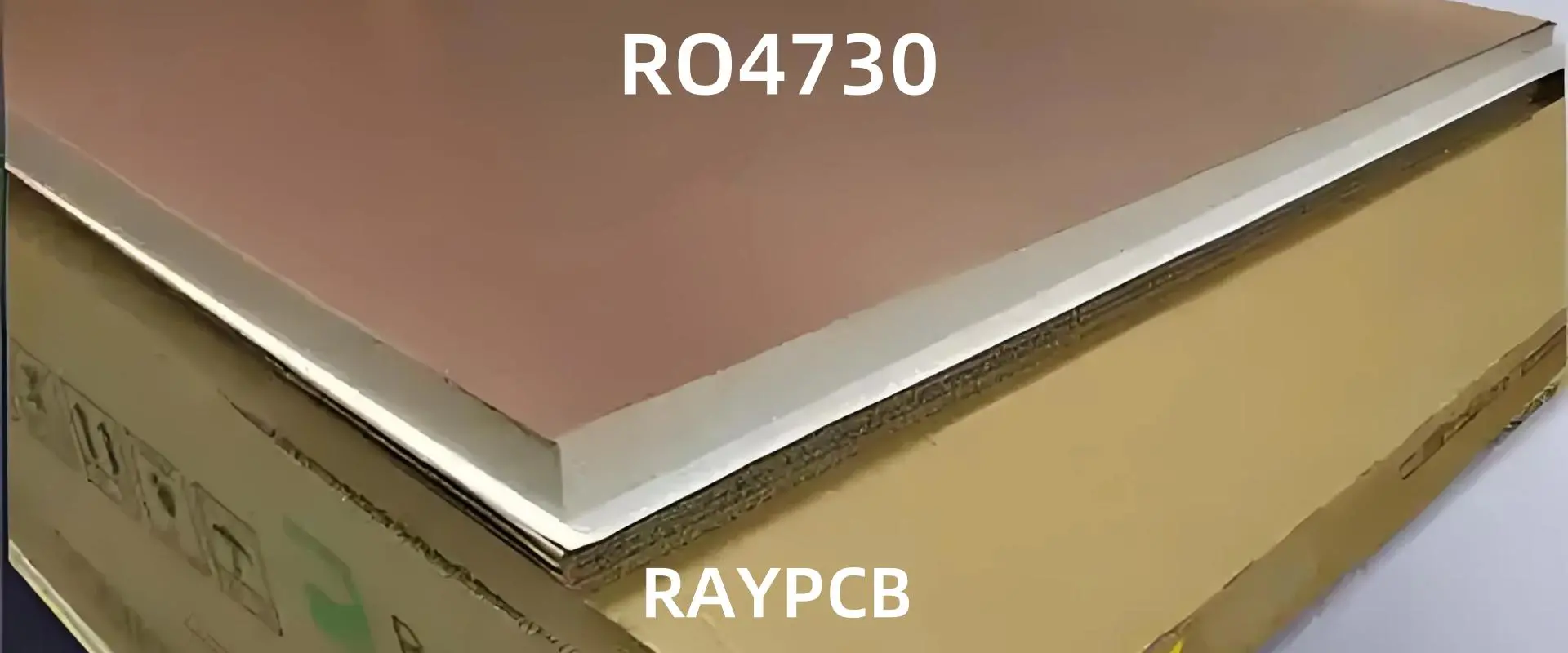
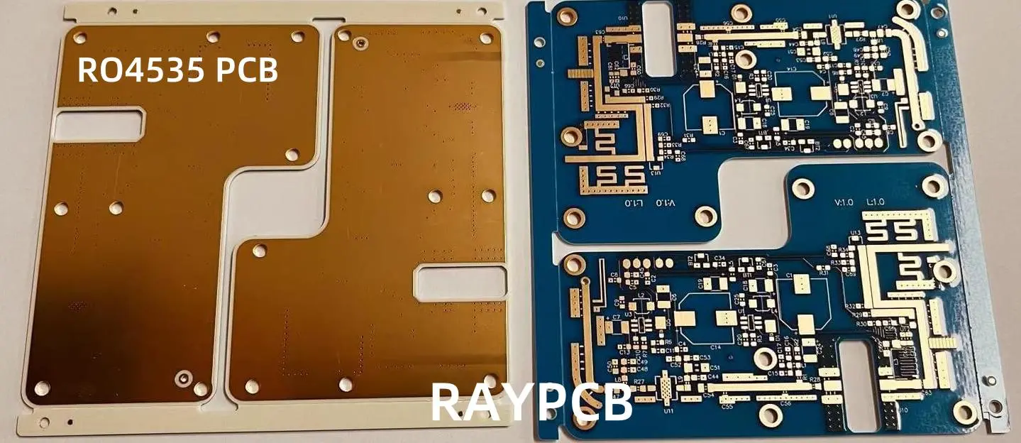
- RO4000® Series
- RT/duroid®
- CLTE-XT™
- AD Series
Each product is presented with its key specifications, making it easy to compare and contrast different materials.
2. Application-Specific Recommendations
One of the standout features of the Rogers Product Selector Guide is its application-specific recommendations. The guide categorizes materials based on their suitability for various applications, such as:
- High-speed digital
- RF/Microwave
- Millimeter-wave
- Antenna systems
- Power amplifiers
This categorization helps users quickly identify the most suitable materials for their specific project requirements.
3. Performance Characteristics
The guide provides detailed information on critical performance characteristics, including:
- Dielectric constant (Dk)
- Dissipation factor (Df)
- Coefficient of thermal expansion (CTE)
- Thermal conductivity
- Moisture absorption
These parameters are essential for engineers to consider when designing high-frequency circuits and systems.
4. Comparative Charts and Graphs
To facilitate easy comparison between different materials, the guide includes visual aids such as:
- Property comparison charts
- Performance graphs
- Application suitability matrices
These visual tools allow users to quickly assess and compare multiple materials side by side.
5. Processing Guidelines
The Product Selector Guide also offers valuable information on material processing, including:
- Recommended fabrication methods
- Drilling and routing guidelines
- Plating recommendations
- Bonding and assembly techniques
This information helps ensure that the selected materials can be effectively integrated into the manufacturing process.
Read more about:
Benefits of Using the Rogers Product Selector Guide

1. Time and Cost Savings
By providing a centralized resource for material selection, the Rogers Product Selector Guide can significantly reduce the time and effort required to identify the most suitable materials for a project. This efficiency can translate into substantial cost savings in the design and development process.
2. Improved Design Optimization
With detailed performance characteristics and application-specific recommendations at their fingertips, engineers can make more informed decisions about material selection. This leads to better-optimized designs and improved overall system performance.
3. Reduced Risk of Material Incompatibility
The comprehensive information provided in the guide helps designers avoid potential pitfalls associated with material incompatibility. By understanding the full range of material properties and processing requirements, engineers can minimize the risk of issues arising during manufacturing or in the final product.
4. Enhanced Innovation
Access to a wide range of high-performance materials and their properties can inspire innovative design solutions. The Rogers Product Selector Guide exposes designers to cutting-edge materials that may open up new possibilities for their projects.
5. Streamlined Procurement Process
For procurement specialists, the guide serves as a valuable reference for understanding material specifications and requirements. This can help streamline the procurement process and ensure that the correct materials are sourced for each project.
Navigating the Rogers Product Selector Guide
Online vs. Print Versions
The Rogers High Frequency Electronics Product Selector Guide is available in both online and print formats. The online version offers the advantage of real-time updates and interactive features, while the print version provides a handy reference for offline use.
Search and Filter Functionality
The online version of the guide typically includes advanced search and filter functionality, allowing users to quickly narrow down their options based on specific criteria such as:
- Dielectric constant range
- Operating frequency
- Thermal performance
- Mechanical properties
Technical Support and Resources
In addition to the product information, the guide often provides links to additional technical resources, including:
- Material datasheets
- Application notes
- Design guidelines
- Technical articles
Users can also find contact information for Rogers’ technical support team, should they need further assistance in material selection or have specific questions about product performance.
Conclusion
The Rogers High Frequency Electronics Product Selector Guide is an essential tool for anyone working with high-frequency electronic materials. By providing comprehensive, easily accessible information on a wide range of high-performance laminates and substrates, the guide empowers engineers and designers to make informed decisions that optimize their designs and improve overall system performance.
As the demand for high-frequency applications continues to grow across industries, tools like the Rogers Product Selector Guide become increasingly valuable. By leveraging this resource, professionals in the field can stay at the forefront of material technology, driving innovation and excellence in high-frequency electronic design.
Whether you’re developing next-generation 5G infrastructure, advanced radar systems, or cutting-edge medical devices, the Rogers High Frequency Electronics Product Selector Guide is an indispensable resource for navigating the complex world of high-performance materials. By making material selection more efficient and informed, Rogers Corporation continues to support the advancement of high-frequency electronics across a diverse range of industries and applications.