6 Methods of DIY PCB Fabrication

pcb high quality guarantee

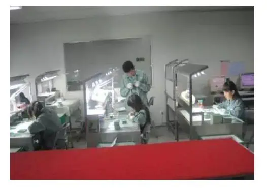
How to Fabricate a PCB With DIY Methods?

YouTube video

Method 1#:

  1. Cut the copper-clad laminate to the size required by the pcb fabrication
  2. Put the stencilpaper on the steel plate, use a pen to draw the circuit diagram on the stencil paper (diagram size should be 1:1), cut it out according to the PCB size, and place it on the copper-clad laminate. Take a small amount of paint and talcum powder into a suitable printing material, dip the printing material with a brush, and evenly apply it to stencil paper. Repeat it several times. Then the circuit can be printed on the printed board. This printed board can be used repeatedly and is suitable for small batch production.
  3. Use 1g of potassium chlorate and 40ml of 15% hydrochloric acid to prepare a corrosive solution, and then apply it to the printed board where it needs to be corroded for corrosion.
  4. Wash corroded printed boards repeatedly with water. Wipe off the paint with banana oil, and then wash it several times to clean theprinted board without leaving corrosive liquids. Apply a layer of rosin solution. Let it dry before drilling.

PCB fabrication Method 2#:

There are many ways amateurs can create PCB, but they are either time-consuming, complex in “craftsmanship,” or low quality. My method of making PCB is one of the methods with a better overall effect. The method is as follows:

  1. Printed circuit board diagram. The pads in the figure are represented by dots, and the connection can be a single line, but the position and size must be accurate.
  2. Cut the printed circuit board according to the circuit diagram’s sizeand clean the surface of the copper foil.
  3. Use carbon paper to copy the diagram to the printing board. If the circuit is simple and the producer has extensive board-making experience, this step can be omitted.
  4. Depending on the components, paste standard pre-cut symbols (pads) with different inner and outer diameters. Then stick tape lines of different widths according to the current. Electronic stores provide standard pre-cut symbols and tape. Common specifications of pre-cut symbols include basic materials such as D373 (0D-2.79, ID-0.79), D266 (0D-2.00, ID-0.80), D237 (OD-3.50, ID-1.50). Try not to use (black) and plastic (red) materials. The general specifications of tape are 0.3, 0.9, 1.8, 2.3, 3.7, etc. The unit is millimeters.
  5. Use a softer hammer, such as smooth rubber, plastic, etc.,to hit the sticker to make it fully adhere to the copper foil. Focus on the turning and overlapping of the line. It is best to use a heater in cold weather to heat the surface to enhance the adhesion effect.
  6. Put it in ferric chloride to start the corrosionprocess. Be noted that the liquid temperature cannot be higher than 40° After corrosion, it should be taken out and rinsed at the correct time, especially if there are thin lines.
  7. Make holes, polish the copper foil with fine sandpaper, apply rosin alcohol solution, and let it dry. The quality of this printed board is very close to that of a conventional printed board. The 0.3 mm tape can be passed between the two legs of the IC, which can greatly reduce the short jumpers on the front of the circuit board, thus saving trouble and time.

PCB fabrication Method 3#:

pcb fabrication
  1. Dissolve lacquer flakes (namely shellac, available from chemical stores) in three parts of absolute alcohol, and stir appropriately. After all the flakes dissolve, add a few drops of medical purple potion (gentian violet) to make it show a particular After evenly mixing, it can be used as protective paint for the pcb fabrication.
  2. First,polish the copper-clad board with fine sandpaper. Then use the duckbill pen in the drawing instrument (or the ink duckbill pen used to draw graphics on the compass) for drawing. There are nuts on the duckbill pen to adjust the thickness of the stroke. You can also use a triangle ruler to draw thin straight lines. The drawn line should be smooth, uniform, without jagged edges, giving people a smooth and fluent feeling. You can also write Chinese characters, English, pinyin, and symbols in the free space of the circuit board.
  3. If the drawing line penetrates the surrounding environment, the concentration is too small,and you can add some paint chips. If the drawing line does not stretch smoothly and becomes too thick, you need to drop a few drops of absolute alcohol. It doesn’t matter if you make a mistake. Just wipe it off with a small cotton swab dipped in absolute alcohol, and then redraw. After drawing the circuit board, it may corrode in the ferric chloride solution. After the circuit board is corroded, it is very convenient to remove the paint. Dip a cotton ball in absolute alcohol to wipe the protective paint to dry, and then apply rosin.
  4. Because the alcohol evaporates quickly, the prepared protective paint should be sealed and stored in a small bottle,such as an ink bottle. Cover the bottle cap after use. If the concentration becomes thicker in the next use, add the appropriate amount of anhydrous alcohol to dilute the solution.

Fabrication PCB Method 4#:

  1. Paste the self-adhesive labels on the copper foil of the copper-clad laminate, then draw the circuit on the veneer. Use a cutter to cut the veneer to form the required circuit prototype, remove the non-circuit parts, and finally use ferric chloride to corrode theideal circuit board.
  2. The corrosion temperature can be performed at about 55°C, and the corrosion rate is more rapid. Rinse the corroded circuit board with clean water, remove the self-adhesive labels on the circuit board, make holes, wipe clean, and then apply rosin alcohol solution prior to

Method 5#:

  1. Arrange the components’ density and positionaccording to the shape of the components used in the schematic circuit diagram and the size of the printed board area. The components‘ location should be determined according to the principle of large first, then small, first overall, and then local. The adjacent components in the circuit are placed nearby and arranged neatly and evenly.
  2. The connecting tracebetween components cannot be bent at right angles at the corners or intersections of the two traces. They must transition through a curve, and they cannot cross each other and turn too far. When certain traces cannot achieve this, you can consider placing printed trace on the back of the printed board and then using stud bolts to connect to the front circuit. Another solution is to use insulated trace when soldering components.
  3. The distance between the input part and the output part is better to avoid mutual interference.

Method 6#:

  1. Print the circuit board diagram on the printer at a ratio of 1:1 on 80 grams of copy paper. Hand drawing is also possible, but the bottom paper should be flat.
  2. Find a fax machine, take out the fax paper from the machine, and replace it with a hot-melt plastic film. Put the circuit diagram into the fax machine’s outgoing fax trayand use the copy button to copy the circuit diagram on the hot-melt plastic film. At this time, the “printed manuscript” of the printed circuit board is ready.
  3. Use double-sided adhesive tape to affix the drawn plastic film to the copper-clad board evenly. The plastic film and board shouldbe flat and not wrinkled. The tape paper can not cover the melted part. Otherwise, it will affect the production quality of the circuit board.
  4. Use a paintbrush to brush the paint on the plastic film evenly. Note: Only brush in one direction. Otherwise,the plastic film will wrinkle, and the lines on the copper plate will overlap. After the circuit diagrams have been brushed, carefully remove the plastic film. At this time, a printed circuit board is finished. After drying, it can be corroded.
  5. If you want to print manypieces, you can make a wooden frame that is a little larger than the circuit board, lay the PCB stencil (our company sells it) flat on the wooden frame, and fix it. Then use double-sided tape to stick the fixed plastic film under the screen. Put the copper-clad board on the table, close the screen frame (the printed image and the copper-clad board should be aligned left and right), use a paintbrush to paint in one direction, and remove the screen frame. The printed circuit board is printed. If there is any defect, it can be modified with paint and bamboo.

Pay attention to the above process. When painting, the hand force should be light and heavy. If there is too much paint or the film is too thick, the lines will be smudged. If the force is too light, the lines will break. And the plastic film must face up.

What is the Industrial PCB fabrication Process?
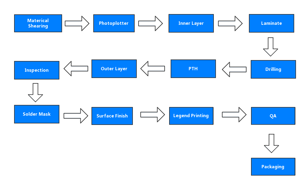
pcb fabrication process
  1. Board cut

Board cutting is the process of cutting the original copper-clad laminate into boards that can be made on the production line.

First, let’s understand a few concepts:

  • UNIT: Refers to the unit graphics designed by PCB design engineers.
  • SET: Refers to multiple units that engineers put together to improve production efficiency and facilitate production. This is what we often call the puzzle, which includes unit graphics, process edges,etc.
  • PANEL: Refers to a pcb fabrication composed of multiple sets. It is added with tool board edges to improve efficiency and facilitate production when PCB manufacturers producethe product.
  1. Innerdry film

The inner layer dry film is the process of transferring the inner layer circuit pattern to the pcb manufacturing board.

In PCB production, we will mention the concept of graphics transfer because the production of conductive graphics is the basis of PCB production. Therefore, the graphics transfer process is of great significance to pcb fabrication process.

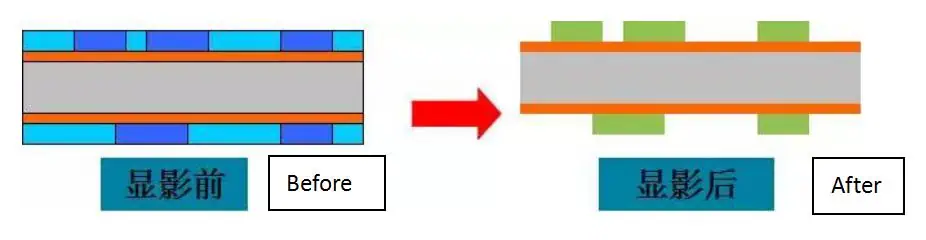
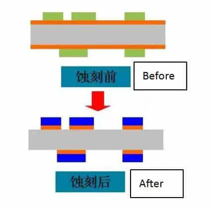
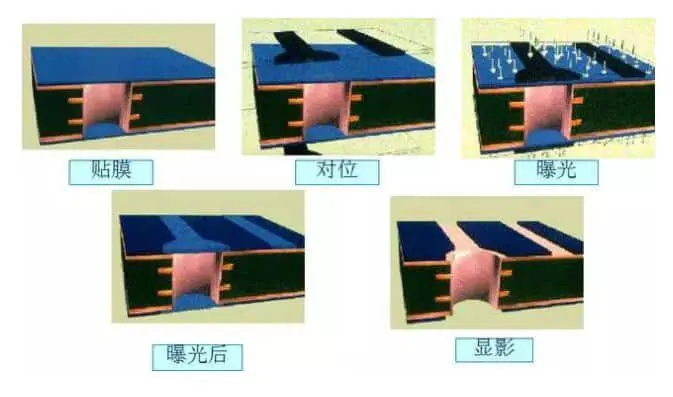
The inner dry film application includes many processes such as inner layer filming, exposure, development, and etching. The inner film is to paste a special photosensitive film on the copper plate’s surface, which we call a dry film. This film will cure when exposed to light, forming a protective film on the board. Exposure and development expose the board with the film, the transparent part is cured, and the non-transparent part is still the dry film. After developing, the uncured dry film is removed, and the board with the cured protective film is etched. After removing the film, the inner circuit pattern is transferred to the board. The whole process flow is shown in the picture below.

pcb fabrication process

For designers, our main consideration is the minimum line width, spacing control, and wiring uniformity. If the distance is too small, it will cause film clamping. If this occurs, the film cannot be removed entirely and will cause a short circuit. If the line width is too small, the film’s adhesion is insufficient, resulting in an open circuit. Therefore, the safety spacing during circuit design (including line to line, line to pad, pad to pad, line to the copper surface, etc.) must be considered during pcb manufacturing.
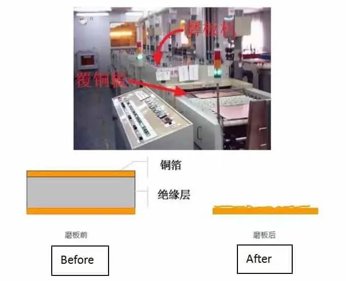
  • Grinding board

The primary function of the grinding plate: The basic pretreatment is mainly to solve the problems of surface cleanliness and roughness. Remove oxidation and increase the copper surface’s roughness, which will increase the film’s adhesion effect to the copper surface.

pcb fabrication diy
  • Filming

Paste the processed substrate with dry film or wet film by hot pressing or coating to facilitate subsequent exposure production.

gerber files for pcb fabrication
  • Exposure

Align the negative film with the substrate on which the dry film is pressed, and use ultraviolet light on the exposure machine to transfer the negative film pattern to the photosensitive dry film.

online pcb fabrication
  • Development

Use the weak alkalinity of sodium carbonate to dissolve and rinse the unexposed dry film/wet film, leaving the exposed part.

pcb fabrication usa
  • Etching

After the unexposed dry film and wet film are removed, the copper surface will be exposed. Use acid copper chloride to dissolve and corrode the exposed copper surface to obtain the required circuit.

prototype pcb fabrication
  • Film stripping

Use sodium hydroxide solution to peel off the exposed dry film that protects the copper surface to expose the circuit pattern.

3. Brown oxidation

Purpose: To form a microscopic roughness and organic metal layer on the inner copper surface to enhance the adhesion between the layers.

Process principle: Through chemical treatment, a uniform and good adhesion characteristic of the organic metal layer structure is produced. The copper layer’s surface, which is before the inner layer, is roughened in a controlled matter. This is to strengthen the inner copper layer and the prepreg after pressing the plate strength.
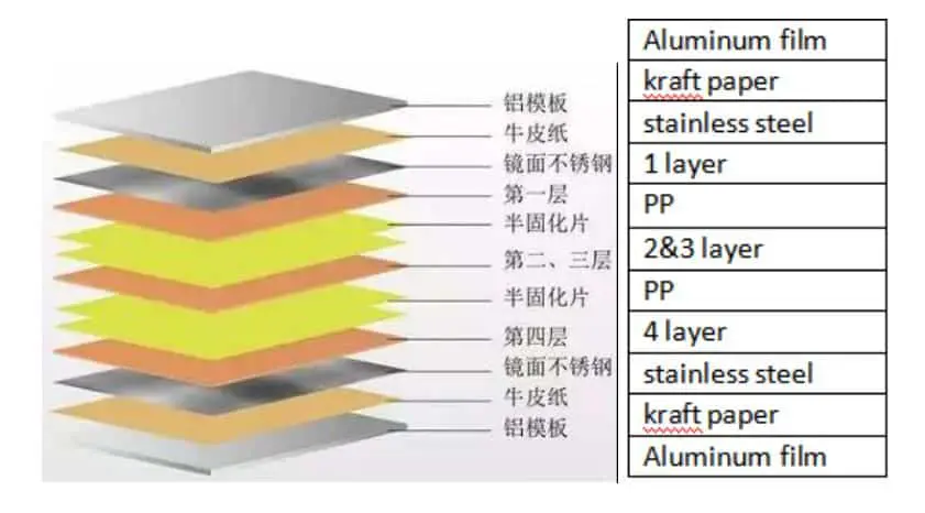
pcb fabrication drawing

4.Stack up

Stack up is the process of bonding each layer into a whole utilizing the PP sheet’s adhesiveness. This bonding is achieved by mutual diffusion, penetration between macromolecules on the interface, and interweaving. The multi-layer pcb manufacturing and PP sheets are pressed together to form a multi-layer board with the required number of layers and thickness. In actual operation, the copper foil, bonding sheet (prepreg), inner layer, stainless steel, isolation board, kraft paper, outer layer, and other materials are laminated according to the process requirements.

multilayer pcb fabrication

For designers, the first consideration for stack up is symmetry. Because the pcb fabrication will be affected by pressure and temperature during the lamination process, stress will remain on the board after the lamination is completed. Therefore, if the two sides of the laminated board are not uniform, the stress on the two sides will be different, causing the board to bend to one side, which greatly affects the PCB’s performance.

In addition, even in the same layer, if the copper distribution is uneven, the resin flow rate at each point will be different. As a result, the area with less copper will be slightly thinner, and the area with more copper will be slightly thicker.

In order to avoid these problems, various factors such as the uniformity of the copper distribution, the symmetry of the stack, the design and layout of the blind and buried holes, etc., must be considered in detail during the design.

5.Drilling

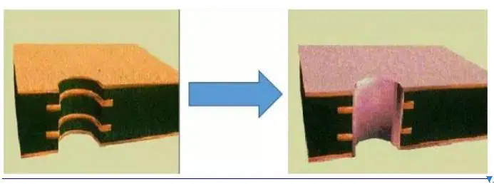
Drilling is the process of creating through-holes between the layers to connect the layers.

pcb fabrication machine

6.Plated through holes(PTH) and plating

  • Plated through holes(PTH)

Plated through-holes are also called chemical copper. After drilling, the PCB board undergoes redox reactions in the sinking copper cylinder to form a copper layer to metalize the holes. Copper is deposited on the surface of the original insulating substrate to achieve an interlayer electrical connection.

hobby pcb fabrication
  • Plating

Plating creates the PCB board surface that has just been copper-immersed. The copper in the hole is thickened to 5-8um to prevent the thin copper in the hole from being oxidized or micro-etched and leaking the substrate before pattern plating.

laser direct imaging pcb fabrication

(1) Outer dry film

The process is the same as the inner dry film.

8.Outer layer pattern plating, SES

The copper layer of the hole and circuit is plated to a specific thickness (20-25um) to meet the copper thickness requirements of the final PCB board. The useless copper on the board surface is etched away, exposing useful circuit patterns.

9. Solder mask

Solder mask, also called and green oil, is one of the most critical PCB fabrication processes. Solder mask is achieved mainly through screen printing or coating solder mask ink, coating a layer of solder mask on the board surface, and developing through exposure. The processes also expose the disk and hole to be soldered and cover other areas with solder mask to prevent short circuit during soldering.

pcb fabrication capabilities

10. Silkscreen

The required text, trademark, or part symbol is printed on the board surface by screen printing. Afterward, it is exposed on the board surface by ultraviolet radiation.

small quantity pcb fabrication

11. Surface treatment

The solderability of bare copper itself is very good, but long-term exposure to the air can cause oxidation and saturation. It tends to exist in the form of oxides and is unlikely to remain as the original copper for an extended period. Therefore, surface treatment of the copper surface is required. The primary purpose of surface treatment is to ensure good solderability or electrical properties.

Regular surface treatments: HASL, immersion gold(ENIG), OSP, immersion tin, immersion silver, electric hard gold, electric gold fingers, etc.

12. Forming

The pcb fabrication process is cut into the required dimensions with a CNC molding machine.

cheap pcb fabrication

13. Electrical test(E-test)

Simulate the status of the pcb fabrication and check the electrical performance after power on to see if there is an open or short circuit.

14. Final inspection, sampling test, packaging

Check the appearance, size, hole diameter, thickness, and marking of the pcb fabrication process to meet customer requirements. The qualified products are packed into bundles, which are easy to store and transport.

pcb fabrication service

What is the difference between a flex circuit and a PCB?

quick turn flexible PCB prototype

Introduction

Printed circuit boards (PCBs) and flex circuits are common technologies used to interconnect electronic components and provide mechanical support. While both utilize conductive traces and pads on an insulating substrate, there are important differences between rigid PCBs and flexible circuits.

This article will examine the variations in materials, construction methods, performance capabilities, and typical applications for flex circuits versus PCBs. Understanding the tradeoffs involved can help designers select the optimal interconnection technology for each system.

PCB Overview

A printed circuit board consists of thin alternating layers of conductive copper and insulating dielectric substrate. The substrate material most commonly used is FR-4 fiberglass, which is rigid and relatively inexpensive. Other rigid laminate materials include FR-5, GETEK, and polyimide.

The board fabrication process generally includes:

  1. Drilling holes for component leads and vias
  2. Electroless copper plating to metallize the holes
  3. Laminating copper foil onto the substrate
  4. Photolithography to print the circuit pattern onto the copper
  5. Etching away unwanted copper to form isolated traces
  6. Applying protective solder mask over the traces
  7. Silkscreen printing of component designators

This subtractive process results in a rigid board with etched copper traces connecting surface mount and through-hole components soldered onto the pads. PCBs can be single, double, or multilayer with traces on both sides and internally between layers.

6 layer FR-4 PCB with surface mount and through-hole components

PCB Attributes:

  • Rigid fiberglass substrate
  • FR-4, FR-5, GETEK, polyimide, ceramic materials
  • Multilayer construction possible
  • High density interconnects
  • Fine line & space traces
  • Plated through hole vias
  • Lower cost process

Flex Circuit Overview

YouTube video

A flex circuit consists of conductive traces and pads on a flexible dielectric substrate material. This allows the circuit to bend and flex dynamically during use. Polyimide films like Kapton or UPILEX are commonly used as the flexible insulating base material.

There are two main methods for creating a flex circuit:

Additive: An additive process is typically used for finer features. Conductive material is selectively deposited onto the substrate through masking and electroplating:

  1. A thin metal foil is laminated onto the substrate.
  2. Photoresist is applied and imaged to define the circuit pattern.
  3. Exposed areas are electroplated to build up the conductor thickness.
  4. Photoresist is stripped away, leaving the plated traces on an etched foil base.

Subtractive: A subtractive process can also create flex circuits, removing unwanted copper similarly to rigid PCB fabrication:

  1. An adhesive layer bonds a copper foil to the flexible substrate.
  2. Photoresist is laminated and imaged with the circuit layout.
  3. Exposed copper is chemically etched away.
  4. The remaining photoresist is stripped off.
flex-circuit-manufacturer

Polyimide flex circuit fabricated with an additive process

Flex Circuit Attributes:

  • Thin flexible substrate
  • Polyimide, PEEK, PET, TPU, PEN materials
  • Difficult to make multilayer
  • Tighter trace routing density
  • Finer lines and spaces
  • Flexible adhesive connections
  • Requires special handling

Physical Construction Comparison

PCBs and flex circuits vary quite a bit in terms of their physical construction and materials used:

ParameterPCBFlex Circuit
SubstrateFR-4, G10, GETEK, BTPolyimide, PEEK, PET
Dielectric Thickness1.6mm, 2.4mm typical25μm – 75μm typical
LayersUp to 30+ layersTypically single layer or double layer
Conductor1oz – 3oz copper foil0.5oz – 2oz rolled annealed copper
Line Width100μm minimum15μm possible
Line Spacing150μm minimum25μm minimum
Via ConstructionPlated through holeMicrovias, filled vias
FlexibilityRigidDynamic flexing capability
WeightHeavierLighter weight

Some key differences to note:

  • PCB substrates are thicker for structural rigidity, while flex circuits use thin flexible polymer films.
  • Multilayer constructions are common with PCBs but challenging with flex circuits.
  • Flex circuits can achieve finer trace widths and pitches.
  • Flex circuits are inherently flexible for dynamic movement requirements.

Performance Comparison

Flexible pcb board cost

The design objectives and use environment drives the performance requirements for an interconnection technology. Here is how PCBs and flex circuits compare for some key parameters:

Electrical Properties

MetricPCBFlex Circuit
Dielectric ConstantFR4: 4.5Polyimide: 3.5
Loss TangentFR4: 0.017Polyimide: 0.003
Insulation Resistance100 TΩ typical20 TΩ typical
Breakdown Voltage23 kV/mm16 kV/mm
Propagation SpeedFR4: 60%Polyimide: 85%
  • Flex circuits generally have lower loss and higher frequency performance.
  • PCBs can operate at higher voltages.
  • Match dielectric materials to application signal frequencies.

Mechanical Properties

MetricPCBFlex Circuit
Young’s ModulusFR4: 20-30 GPaPolyimide: 2.5 GPa
Tensile StrengthFR4: 275 MPaPolyimide: 231 MPa
Flexural RigidityVery low flexibilityCan bend dynamically
Thermal ExpansionFR4: 12-16 ppm/CPolyimide: 20 ppm/C
  • PCBs are rigid with high stiffness.
  • Flex circuits are flexible but have lower strength.
  • Coefficient of thermal expansion varies.

Environmental Resistance

MetricPCBFlex Circuit
Flammability RatingFR4: V-0Polyimide: V-0
Moisture AbsorptionFR4: 0.2%Polyimide: 2.0%
Chemical ResistanceFair acrylics, alcoholsGood overall
UV TolerancePoor – yellowsExcellent UV stability
Operational TemperatureFR4: 130°CPolyimide: 260°C
  • Both meet flammability standards for electronics.
  • Polyimide has broad chemical resistance.
  • Flex circuits withstand higher temperatures.

PCB vs. Flex Circuit Layout Comparison

The different construction and capabilities of PCBs and flex circuits require adapted layout strategies.

For PCBs, common practices include:

  • Partitioning circuits across multiple rigid layers
  • Escape routing component leads with clearance for etch and drilling
  • Area fills for power and ground planes
  • Grid-based placement with fixed 90° routing
  • High density surface mount components on both sides
  • Matching trace widths to current requirements
  • Impedance control traces and serpentine length matching

Flex circuit layout is characterized by:

  • Constrained to 1-2 flexible layers
  • Tight component placement and routing density
  • Curved traces following substrate contours
  • Selective reinforcements and stiffeners
  • Avoiding 90° traces and joints during flexing
  • Adhesive openings to isolate rigid sections
  • Careful management of cross-section changes
  • Fabrication-aware keepout margins

These examples illustrate the differing approaches needed to optimize layouts.

Typical Applications

Due to their distinct properties, PCBs and flex circuits tend to be used in very different types of products and assemblies.

Common PCB Applications:

  • Computer motherboards and expansion cards
  • Consumer electronics like phones and tablets
  • Telecommunications infrastructure equipment
  • Automotive engine control units (ECUs)
  • Industrial control systems
  • Power electronic converters
  • LED lighting drivers

PCBs provide an inexpensive rigid interconnection foundation for electronic subsystems and complex digital circuits. The modular nature allows assembly and servicing of individual boards.

Common Flex Circuit Applications:

  • Printers and scanners
  • Computer disk drives
  • Robotic arms
  • Medical imaging equipment
  • Fitness trackers and wearables
  • Avionics systems
  • Automotive sensors
  • High temperature electronics

When dynamic flexing, tight space constraints, or projected lifetime motion cycles are involved, flex circuits can provide reliable interconnects without wires or connectors. The continuous constructions allows flex circuits to fit product industrial design needs.

Cost Considerations

For low volume, PCBs generally have a lower cost per unit compared to flex circuits. The reasons include:

  • Economies of scale with massive worldwide PCB production volumes
  • Lower cost raw materials like standard FR-4
  • Highly automated fabrication processes
  • Mature assembly ecosystems and acceptance testing

As production quantities scale, flex circuits can reach similar price points for an overall system. Other considerations like these can also impact cost:

  • Layer count – Multilayer PCBs get exponentially more expensive
  • Fabrication yield – Thin flex circuits can have more waste
  • Connectors avoided – Flex circuits eliminate these costs
  • Testing – Both require verification time and overhead
  • Serviceability – Repairing flex circuits may require full replacement

The optimal choice involves weighing production volume, system complexity, product lifecycle, and manufacturing strategy tradeoffs.

Hybrid PCB/Flex Applications

In some cases, combining rigid PCBs with flex circuits provides an ideal solution. Some examples include:

  • Hinge connections: Flex circuits folding around a corner or hinge to interconnect PCBs. Used extensively in flip phones and laptops.
  • Screen connections: Flexible circuits connecting a display or touchscreen behind a device cover to the main PCB. Allows full range of adjustability.
  • Sensor arrays: Flex circuits create dynamic conformal sensor grids that attach to rigid sensor hub PCBs. Used in robotic skin, building HVAC monitors, and body networks.
  • Wearables: A rigid PCB provides processing and wireless functions, while flex circuits interconnect across clothing and accessories. Seen in rings, watches, and fitness bands.
  • Printers: Flex circuits span the moving print head assembly while connecting to controller boards. Also used in cameras and scanners.

For these applications, flex circuits essentially act as 3D interconnects integrated with planar PCBs when needed.

Summary and Recommendations

Here are some best practices based on the PCB and flex circuit comparison:

  • Select PCBs for static rigid boards with multilayer needs or high voltage.
  • Use flex circuits when flexibility, tight space, or motion cycling are critical.
  • Combine both technologies in a system when needed for modular and dynamic functions.
  • Match dielectric material properties to required performance characteristics.
  • Account for fabrication yield, testing, and serviceability costs.
  • Adapt layout and component selection to the properties of each technology.
  • Seek expert guidance to ensure a reliable design optimized for manufacturability.

Understanding these fundamental differences between printed circuit boards and flex circuits allows designers to make informed tradeoffs and utilize each technology appropriately.

FQA

What are the main differences between flex circuits and rigid PCBs?

The main differences are the flexible substrate material, thinner dielectric layers, finer traces, and dynamic flex capability of flex circuits versus the rigid multilayer FR4 construction and lower cost of traditional PCBs.

Why choose a flex circuit over a PCB?

Use flex circuits when the application requires tight space constraints, dynamic motion and flexing, or conformal shape adaptation that rigid boards cannot provide.

What are some examples of typical flex circuit applications?

Common uses include printers, disk drives, robotic joints, medical equipment, wearables, avionics, and automotive sensors. The flex circuits can adapt to motion and space requirements that PCBs cannot.

What are some typical applications for conventional PCBs?

PCBs are well suited for computers, servers, telecom systems, control systems, LED lighting, and consumer electronics where rigid support for multilayer digital circuits is acceptable.

When does using both PCBs and flex circuits together make sense?

PCB and flex circuit hybrid assemblies provide advantages in applications like laptops, wearables, printers, and sensors that have both dynamic flexible interconnections and rigid support or multilayer circuit needs.

PCB Thermal Conductivity Performance: FR4 Vs. Ceramic Vs. Metal Core Vs. Rogers

Introduction

Managing heat dissipation is critical for reliable and efficient PCB design. The choice of printed circuit board substrate material has a major impact on thermal performance. Materials like FR4, ceramic, metal core PCBs, and Rogers laminates each provide different thermal conductivity properties.

This article compares the thermal characteristics of common PCB substrate types. We’ll examine the composition, thermal conductivity, dielectric properties, design considerations, and typical applications for each material class. With an understanding of material thermal capabilities, PCB designers can select the optimal approach for their thermal management needs.

Thermal Conductivity Basics

Ceramic PCB Thermal Conductivity

Thermal conductivity indicates how effectively a material transports heat. It is defined as:

K = Q x L / A x ΔT

Where:

K = Thermal conductivity in W/m-K

Q = Heat flow rate in Watts

L = Material thickness in meters

A = Material cross sectional area in m^2

ΔT = Temperature difference across material in Kelvin

Materials with higher thermal conductivity (K) values conduct heat more efficiently across a temperature gradient.

For PCBs, thermal conductivity directly impacts how much heat from components and traces flows into the board substrate, as well as spreading across the substrate internally. This heat must ultimately be dissipated to avoid temperature buildup.

FR4 Thermal Performance

fr4 thermal conductivity

FR4 glass reinforced epoxy is the most common and cost effective rigid PCB substrate. However, it suffers from poor thermal conductivity:

Composition

FR4 consists of layers of fiberglass fabric reinforcements impregnated with an epoxy resin binder. The glass fibers provide mechanical rigidity while epoxy gives adhesion and environmental resistance.

Typical multilayer FR4 PCB construction

The glass content typically ranges from 30% to 70% by weight depending on thickness. Higher fiber content increases thermal conductivity but reduces dielectric strength.

Thermal Conductivity

The thermal conductivity of FR4 is highly anisotropic due to the woven fiberglass layers:

  • In-plane (X-Y direction) = 0.25 – 0.30 W/m-K
  • Through-plane (Z direction) = 0.10 – 0.20 W/m-K

The in-plane conductivity is 2-3X higher than through thickness. But even in-plane, FR4 is a very poor conductor compared to metals or ceramics.

Design and Performance Challenges

The limited through-plane conduction hinders heat spreading from hot components into the board:

FR4 exhibits poor thermal spreading from localized heat sources

High power components can experience considerable temperature rise with FR4, risking reduced reliability and performance. Adding thermal vias helps somewhat but is limited by low through-thickness conductivity.

Typical FR4 Applications

Despite thermal constraints, FR4 excels in many applications:

  • Consumer electronics
  • Computers and peripherals
  • Automotive electronics
  • Cost-driven designs
  • Moderate temperature environments

FR4 provides the most affordable PCB substrate for many commercial and industrial products not needing advanced thermal performance.

Ceramic PCB Thermal Performance

Ceramic printed circuit boards provide an order of magnitude better thermal conductivity than FR4, though at higher cost:

Composition

Ceramic PCB substrates consist of aluminum oxide (alumina) or aluminum nitride ceramic filler particles combined with a glassy binding matrix. This produces a crystalline ceramic material.

Common material grades include:

  • Alumina (Al2O3) – 92% to 99% purity
  • Aluminum nitride (AlN) – Over 90% purity

A metal layer (copper, aluminum) typically clads the ceramic base to enable circuit patterning.

Aluminum nitride ceramic PCB

Thermal Conductivity

The thermal conductivity of ceramic PCB materials far surpasses traditional FR4:

  • Alumina: 24 – 30 W/m-K
  • Aluminum nitride: 170 – 250 W/m-K

This enables efficient lateral and vertical heat spreading. The high purity minimizes defects that would impede heat transfer.

Design and Performance

The excellent thermal conduction allows heat to spread across a larger board area:

Aluminum nitride ceramic exhibits superior thermal spreading

Ceramic PCBs can dissipate very high component heat fluxes while maintaining lower temperatures. The rigid structure also resists warping.

Typical Ceramic PCB Applications

The cost of ceramic material relegates usage to high performance and reliability applications:

  • High power electric vehicle inverters and charging
  • Power supply converters
  • Industrial power and control
  • RF and microwave boards
  • Hybrid microelectronics
  • Aerospace and defense electronics

Ceramic PCBs support the demands of power electronics and microwave circuits where thermal and dielectric performance are critical.

Metal Core PCB Thermal Performance

Metal core PCBs utilize a thick metal base layer to maximize heat spreading and thermal mass:

Composition

Metal core PCBs contain a 0.8mm to several mm thick aluminum or copper layer at the core. Dielectric material layers bond circuit layers to the metal foundation.

Typical metal core PCB construction

Common dielectric layers include polyimide films, epoxy composites, and ceramic substrates. Direct Bonded Copper (DBC) integrates a ceramic layer.

Thermal Conductivity

The metal base provides exceptional thermal conduction:

  • Aluminum: 150 – 230 W/m-K
  • Copper: 400 W/m-K

This enables large heat quantities to be absorbed and spread over the entire board. The thermal mass also promotes lateral conduction.

Design and Performance

Metal core PCBs manage the most extreme thermal loads:

Metal core heat spreading and sinking

The thick metal base acts as both a heat spreader and heatsink, ideal for high power densities. Heat can also be removed via the backside.

Typical Metal Core PCB Applications

The cost and specialized fabrication restricts metal core PCBs to very high power products:

  • Power converters and inverters
  • Motor drives
  • Power amplifiers
  • High brightness LED lighting
  • Wind and solar power electronics
  • Electric vehicle drives

If thermal performance is the paramount priority, metal core PCBs conduct heat extremely efficiently.

Rogers Laminates Thermal Performance

PCB thermal resistance

Rogers Corporation (Chandler, AZ) produces premium PCB substrate materials focused on high frequency applications. Many of Rogers’ circuit materials also offer improved thermal conductivity over FR4 while being cost-effective for high volume commercial products:

Composition

Rogers’ materials utilize fluoropolymer resin systems reinforced with glass fabric. Some products incorporate ceramic filler particles to enhance thermal performance.

Typical Rogers laminate PCB construction

Popular materials include RO4350, RO4003, RT/duroid 6202, and LoPro series laminates. They exhibit a good balance of electrical and thermal properties not found in FR4.

Thermal Conductivity

Rogers’ circuit materials span a wide thermal conductivity range:

These values approach ceramic substrate performance levels while using conventional PCB processes.

Design and Performance

Rogers laminates manage heat dissipation effectively while supporting high speed signal designs:

Rogers materials allow strong in-plane heat spreading

Lower thermal resistance improves power handling for a given temperature rise. The coefficient of thermal expansion is also compatible with common FR4 and copper.

Typical Rogers Laminate Applications

The electrical and thermal properties suit Rogers materials to:

  • High frequency analog and RF PCBs
  • High speed digital designs
  • Power amplifiers
  • LED lighting
  • Automotive circuits
  • Motor drives
  • Semiconductor testing boards

Rogers PCB substrates balance dielectric, thermal, and economic factors for commercial electronics needs.

Thermal Performance Comparison

Here is a summary comparison of the thermal conductivity properties of common PCB substrate types:

MaterialCompositionThermal Conductivity
FR4Epoxy + fiberglass0.25 W/m-K (in-plane)
Ceramic PCBAlumina or AlN25 – 250 W/m-K
Metal core PCBAluminum or Copper core150 – 400 W/m-K
Rogers LaminatesFluoropolymers0.7 – 1.7 W/m-K

This demonstrates the wide range of material options depending on required conductivity levels.

Conclusion

Thermal Clad PCB
Thermal Clad PCB

Managing PCB thermal performance requires selecting substrate materials suited to heat dissipation needs:

  • FR4 provides a low cost PCB material but suffers thermally
  • Ceramic PCBs offer 10-100X better thermal conductivity
  • Metal core PCBs maximize spreading and heat sinking
  • Rogers laminates balance thermal, electrical, and cost factors

Understanding the composition, thermal characteristics, and typical applications guides appropriate material selection. Thermal modeling informs necessary conductivity levels and guides design tradeoffs.

With the right PCB substrate materials in their toolkit, engineers can develop designs meeting their exact thermal management and performance requirements.

FQA

How does thermal conductivity relate to temperature rise for a given heat dissipation level?

Thermal conductivity determines how efficiently heat transfers through a material. Higher conductivity reduces thermal resistance, lowering component junction temperatures for the same power level.

What are the main reasons higher performance PCB materials like ceramics cost more than FR4?

Reasons include more expensive base materials, thinner substrates requiring tighter process controls, lower fabrication yields, and more specialized fabrication equipment and methods.

When does it make sense to use a more expensive ceramic or metal core PCB instead of standard FR4?

Applications warranting premium materials are RF/microwave boards, power electronics, high brightness LEDs, and other products requiring removal of high heat fluxes that exceed FR4 capabilities.

What are some ways to enhance FR4 thermal conductivity?

Adding more copper layers or planar copper increases conductivity marginally. Thermal vias help conduct heat between layers. But large heat sinks are often still required with FR4.

How does dielectric constant correlate with thermal conductivity in PCB substrates?

Lower dielectric constant materials like fluoropolymers or ceramics generally have higher thermal conductivity than epoxy/glass composites. But other factors like filler contents also affect conductivity.

Medical PCB Manufacturing: How to Choose a Supplier for Quality, Compliance & Fast Turnaround

medical grade pcb

In the rapidly evolving healthcare industry, selecting the right printed circuit board (PCB) supplier for medical devices is crucial. This comprehensive guide explores the world of medical PCBs, their benefits, types, challenges, and the essential factors to consider when choosing a supplier. Whether you’re a medical device manufacturer or a healthcare technology innovator, this article will provide valuable insights into ensuring quality, speed, and compliance in your medical PCB production.

What is Medical PCB?

A medical PCB is a specialized printed circuit board designed and manufactured for use in medical devices and equipment. These PCBs are crucial components in various healthcare applications, from diagnostic tools to life-support systems. Medical PCBs must meet stringent quality standards and regulatory requirements to ensure patient safety and device reliability.

Benefits of Medical PCB in the Medical Industry

The integration of advanced PCBs in medical devices has revolutionized healthcare delivery. Here are some key benefits:

Mobile Health

Medical PCBs enable the development of portable and wearable health monitoring devices, allowing patients to track their vital signs and health metrics on the go. This technology facilitates remote patient monitoring and telemedicine, improving access to healthcare services.

Health Record Management

PCBs in medical devices support the digitization and secure storage of patient health records. This integration enhances data accuracy, accessibility, and interoperability among healthcare providers, leading to better-informed medical decisions.

Wireless Communication

Advanced medical PCBs incorporate wireless communication technologies, enabling seamless data transfer between medical devices and healthcare information systems. This capability supports real-time patient monitoring and rapid response to medical emergencies.

Data-Based Drugs

PCBs in smart drug delivery systems allow for precise, data-driven medication administration. These systems can adjust dosages based on patient data, improving treatment efficacy and reducing side effects.

Wearables

Medical-grade PCBs are at the heart of wearable health devices, from fitness trackers to continuous glucose monitors. These devices empower patients to take an active role in managing their health and provide valuable data to healthcare providers.

Main Types of PCB for Medical Devices

Medical devices utilize various types of PCBs, each suited for specific applications:

Single Layer Medical PCB

These simple, cost-effective PCBs are used in basic medical devices with low complexity circuits. They’re suitable for devices like digital thermometers or simple monitoring equipment.

Double Layer Medical PCB

Double layer PCBs offer increased circuit density and are commonly used in more complex medical devices, such as blood pressure monitors or portable ECG machines.

Multilayer Medical PCB

Multilayer PCBs are essential for advanced medical equipment that requires high component density and complex circuitry. They’re often found in imaging systems, patient monitors, and diagnostic devices.

Rigid Medical PCB

Rigid PCBs provide stability and durability, making them ideal for stationary medical equipment like MRI machines or hospital bed control systems.

Flexible Medical PCB

Flexible PCBs allow for compact, lightweight designs and are crucial in wearable medical devices and implantable medical technologies.

Rigid-Flex Medical PCB

Combining the benefits of both rigid and flexible PCBs, rigid-flex boards are used in medical devices that require both durability and flexibility, such as ultrasound probes or endoscopic cameras.

HDI Medical PCB

High-Density Interconnect (HDI) PCBs enable the miniaturization of medical devices while maintaining high functionality. They’re essential in compact, feature-rich devices like hearing aids or insulin pumps.

Read more about:

Medical PCB Challenges

Designing and manufacturing PCBs for medical devices presents unique challenges:

Reliability

Medical PCBs must operate flawlessly in critical situations. Ensuring long-term reliability under various environmental conditions is paramount.

Size Constraints

Many medical devices require compact PCBs without compromising functionality. This demand drives the need for advanced PCB technologies and design techniques.

Compliance and Regulatory Requirements

Medical PCBs must adhere to strict regulatory standards, including FDA regulations and ISO certifications. Compliance with these requirements adds complexity to the design and manufacturing process.

How to Design and Fabricate Medical Grade PCB

Illustration of Medical PCB

Creating a medical-grade PCB involves several crucial steps:

1. Create Initial Schematic Design

Develop a comprehensive schematic that accurately represents the circuit’s functionality and component interactions.

2. Prepare Layout

Translate the schematic into a physical PCB layout, considering factors like signal integrity, power distribution, and thermal management.

3. Consider and Add Crucial Factors

Incorporate design elements that address EMI/EMC compliance, biocompatibility, and sterilization requirements specific to medical devices.

4. Split Power Properly

Implement proper power plane design and voltage regulation to ensure stable and clean power distribution across the PCB.

5. Allow Multiple Layers

Utilize multilayer designs to optimize signal routing, reduce EMI, and improve overall PCB performance.

6. Review BOM (Bill of Materials) List

Carefully select and verify components, ensuring they meet medical-grade quality standards and have long-term availability.

7. Check Components

Verify the electrical and physical characteristics of each component, ensuring compatibility with the PCB design and medical device requirements.

8. Prepare and Verify an Alternative Component List

Develop a list of approved alternative components to mitigate supply chain risks and ensure long-term product sustainability.

9. Make a Drawing for the Assembly

Create detailed assembly drawings to guide the manufacturing process and ensure consistent production quality.

10. Show Test Points in the Design

Incorporate strategically placed test points to facilitate in-circuit testing and quality assurance processes.

11. Medical PCB Prototyping and Manufacturing Process

Engage in iterative prototyping and rigorous testing before moving to full-scale production, ensuring the PCB meets all performance and regulatory requirements.

Testing Standards to be Followed for Medical PCBs

Medical Devices pcb
Medical Devices pcb

Rigorous testing is essential to ensure the reliability and safety of medical PCBs:

Automated Optical Inspection (AOI)

AOI systems detect visual defects in PCB assembly, ensuring manufacturing quality and consistency.

Solderability Test

This test verifies the quality of solder joints, crucial for the long-term reliability of medical PCBs.

Ionic Contamination Testing

Ensures the PCB is free from ionic contaminants that could lead to corrosion or electrical failures over time.

Peel Test

Measures the adhesion strength between PCB layers, critical for the durability of multilayer boards.

Micro-sectioning Analysis

Examines the internal structure of PCBs, verifying proper layer alignment and via formation.

Flying Probe Test

Provides comprehensive electrical testing of PCB assemblies, detecting open circuits, short circuits, and component values.

Time-Domain Reflectometer (TDR)

Analyzes signal integrity and impedance matching in high-speed PCB designs.

Quality Management and Compliance Requirements

Medical PCB Manufacturer

Medical PCB manufacturers must adhere to stringent quality and regulatory standards:

ISO Regulations

Compliance with ISO 13485 for medical device quality management systems is essential.

IPC Regulations

Adherence to IPC standards ensures consistency in PCB design, manufacturing, and quality assurance.

FDA Regulations

Medical PCBs must comply with FDA regulations, including 21 CFR Part 820 for quality system requirements.

Longevity Requirements

Medical PCBs often need to support devices with long lifecycles, requiring careful component selection and design for long-term reliability.

How RayMing Meets Your High-Reliability Medical PCB Requirements with Full Traceability

RayMing PCB & Assembly, as a leading medical PCB supplier, offers comprehensive documentation and quality assurance:

Certificate of Conformance

Provides formal certification that the PCBs meet all specified requirements and standards.

Material Specifications

Detailed documentation of all materials used in PCB fabrication, ensuring compliance with medical-grade requirements.

First Article Inspection Report

Comprehensive inspection report of the first production run, verifying design and manufacturing quality.

Reflow Profile Copy

Documentation of the reflow soldering process parameters, ensuring consistent assembly quality.

Photo Requirements

High-resolution images of PCB assemblies for visual verification and documentation.

IPC J-STD-001E Compliance

Adherence to IPC standards for soldered electrical and electronic assemblies.

Calibrated Tool Records

Detailed records of all calibrated tools used during the manufacturing process, ensuring measurement accuracy.

AOI or Visual Inspection Report

Comprehensive reports from automated or manual visual inspections, documenting PCB quality.

Flying Probe or In-Circuit Testing Report

Electrical test reports verifying the functionality and integrity of PCB assemblies.

Ionic Cleanliness Test Report

Documentation of ionic contamination levels, ensuring PCB cleanliness meets medical-grade standards.

Conclusion

Choosing the right PCB supplier for medical devices is crucial for ensuring quality, speed, and compliance in the development of healthcare technologies. By understanding the unique requirements of medical PCBs and partnering with a supplier like RayMing PCB & Assembly that offers comprehensive quality management and traceability, medical device manufacturers can confidently produce reliable, compliant, and innovative healthcare solutions.

When selecting a medical PCB supplier, consider their expertise in medical-grade PCB design, their adherence to regulatory standards, and their ability to provide comprehensive documentation and quality assurance. With the right partner, you can navigate the complexities of medical PCB production and bring life-saving technologies to market efficiently and reliably.

Military PCB Design & Manufacturing: A Complete Guide to MIL-SPEC Compliance

Military PCB Manufacturing

Introduction

In the high-stakes world of defense and aerospace, the reliability and performance of electronic systems can mean the difference between mission success and failure. At the heart of these critical systems lie Military PCBs (Printed Circuit Boards), the unsung heroes that enable everything from advanced communication networks to sophisticated weapons systems. These specialized PCBs are designed and manufactured to withstand extreme conditions, ensure unwavering reliability, and meet the stringent standards set by military specifications.

This comprehensive guide delves into the intricate world of Military PCB design and manufacturing, exploring the crucial factors that set these boards apart from their commercial and industrial counterparts. We’ll examine the stringent MIL-SPEC standards that govern their production, the unique materials and processes involved, and the best practices that ensure these PCBs meet the demanding requirements of modern military applications.

Whether you’re a defense contractor, an engineer working on aerospace projects, or simply interested in understanding the pinnacle of PCB technology, this article will provide you with invaluable insights into the world of Military PCBs. Let’s embark on this journey to uncover how durability, precision, and compliance converge to create the backbone of military electronics.

1. What Is a Military PCB?

Definition of Military PCB

A Military PCB is a specialized printed circuit board designed and manufactured to meet the rigorous standards and specifications required by military and aerospace applications. These PCBs are engineered to operate reliably in extreme environments and under harsh conditions that would cause standard commercial PCBs to fail.

How Military PCBs Differ from Commercial and Industrial PCBs

Military PCBs stand apart from their commercial and industrial counterparts in several key aspects:

  1. Durability: Built to withstand extreme temperatures, shock, vibration, and humidity.
  2. Reliability: Engineered for extended operational life and minimal failure rates.
  3. Performance: Designed to maintain signal integrity under challenging conditions.
  4. Compliance: Adherence to strict military standards and specifications (MIL-SPECs).
  5. Materials: Use of high-grade, specially certified materials.
  6. Manufacturing Process: Rigorous quality control and documentation throughout production.
  7. Testing: Extensive testing protocols to ensure performance and reliability.

Common Applications of Military PCBs

Military PCBs find their way into a wide array of critical defense and aerospace systems, including:

  • Advanced communication systems
  • Radar and sonar equipment
  • Avionics and flight control systems
  • Missile guidance systems
  • Satellite technology
  • Electronic warfare systems
  • Rugged portable devices for field operations
  • Unmanned aerial vehicles (UAVs) and drones

2. Key Requirements for Military PCB Design

Durability Under Extreme Conditions

Military PCBs must be designed to operate reliably in environments that would quickly degrade or destroy standard electronics. This includes:

  • Temperature Extremes: Functioning in temperatures ranging from -55°C to +125°C or beyond.
  • Vibration and Shock: Withstanding high G-forces and constant vibration in aircraft and vehicles.
  • Radiation Resistance: Operating in high-altitude or space environments with increased radiation exposure.
  • Humidity and Moisture Resistance: Maintaining integrity in high-humidity or potentially wet conditions.

High Reliability and Long Lifecycle

The nature of military operations demands electronics that won’t fail at critical moments and can remain in service for extended periods. This requires:

  • Component Selection: Using military-grade, high-reliability components.
  • Redundancy: Implementing redundant circuits and fail-safe designs.
  • Thermal Management: Effective heat dissipation to prevent premature component failure.
  • Lifecycle Planning: Designing for long-term availability of components and potential future upgrades.

EMI/EMC Considerations in Design

Electromagnetic Interference (EMI) and Electromagnetic Compatibility (EMC) are crucial factors in military electronics:

  • Shielding: Implementing effective EMI shielding techniques.
  • Layout Strategies: Careful PCB layout to minimize EMI generation and susceptibility.
  • Filtering: Incorporating appropriate filtering components to reduce EMI.
  • Grounding: Proper grounding techniques to manage electromagnetic emissions and susceptibility.

Secure and Redundant System Design for Mission-Critical Operations

Military PCBs often form the backbone of mission-critical systems where failure is not an option:

  • Fault Tolerance: Designing systems that can continue to function even if part of the circuit fails.
  • Secure Design: Implementing features to prevent unauthorized access or tampering.
  • Data Protection: Incorporating encryption and secure communication protocols at the hardware level.
  • Redundant Power: Ensuring uninterrupted operation through redundant power supplies and circuits.

3. Understanding MIL-SPEC Standards

What are MIL-SPECs and Why They Matter

Military Specifications (MIL-SPECs) are a set of standards issued by the United States Department of Defense to ensure uniformity, quality, and reliability in military and aerospace equipment. For PCBs, these standards define:

  • Material requirements
  • Design parameters
  • Manufacturing processes
  • Testing procedures
  • Documentation and traceability requirements

Adherence to MIL-SPECs is crucial because it:

  • Ensures interoperability between different systems and components
  • Guarantees a minimum level of quality and reliability
  • Facilitates the procurement process for military projects
  • Provides a common language between manufacturers and military customers

Key Military Standards Impacting PCB Design

MIL-PRF-31032 (Performance Specifications)

This specification covers the general requirements for printed circuits, including:

  • Qualification and performance requirements
  • Quality assurance provisions
  • Marking and traceability

MIL-PRF-55110 (Rigid PCBs)

Focused on rigid printed circuit boards, this standard specifies:

  • Material requirements for rigid PCBs
  • Design and construction parameters
  • Testing and inspection criteria

MIL-PRF-50884 (Flexible PCBs)

This standard addresses the requirements for flexible and rigid-flex printed circuits:

  • Flex and rigid-flex material specifications
  • Design guidelines for flexible circuits
  • Unique testing requirements for flex PCBs

IPC-A-610 Class 3 (Acceptability of Electronic Assemblies)

While not a military standard per se, IPC-A-610 Class 3 is often specified for military projects:

  • Defines the highest level of acceptance criteria for electronic assemblies
  • Covers various aspects of PCB assembly, including soldering, component mounting, and cleanliness

How Compliance Impacts Procurement and Deployment in Military Projects

Compliance with MIL-SPECs has far-reaching implications:

  1. Qualification Process: Manufacturers must undergo rigorous qualification processes to be certified for military PCB production.
  2. Cost Considerations: Meeting MIL-SPEC requirements often increases production costs but is necessary for ensuring reliability.
  3. Lead Times: Compliance can lead to longer lead times due to additional testing and documentation requirements.
  4. Supply Chain Management: Only certified suppliers can be used, impacting the entire supply chain.
  5. Project Approval: Non-compliance can lead to project delays or rejections in military procurement processes.
  6. Field Performance: MIL-SPEC compliance directly impacts the reliability and performance of deployed military systems.

4. Materials Used in Military PCBs

Military Electronics

High-Tg and Low-CTE Laminates

Military PCBs often utilize specialized laminates with specific characteristics:

  • High Glass Transition Temperature (Tg): Materials like polyimide that maintain stability at high temperatures.
  • Low Coefficient of Thermal Expansion (CTE): To minimize warping and stress on components during temperature fluctuations.
  • Examples: Rogers 4350B, Isola IS620, and Panasonic MEGTRON6.

Metal Core PCBs for Thermal Management

In applications requiring superior heat dissipation:

  • Aluminum or copper core PCBs are used to efficiently conduct heat away from components.
  • These PCBs can handle higher power densities, crucial for radar and high-power RF applications.

Special Surface Finishes

Military PCBs often require specialized surface finishes for enhanced durability and reliability:

  • ENIG (Electroless Nickel Immersion Gold): Provides excellent corrosion resistance and solderability.
  • Hard Gold: Used in applications requiring high wear resistance, such as edge connectors.
  • HASL (Hot Air Solder Leveling): Still used in some military applications, though less common due to lead concerns.

High-Reliability Solder Materials

Solder selection is critical in military PCBs:

  • Lead-based solders: Still used in some military applications due to their reliability and exemption from RoHS regulations.
  • High-reliability lead-free alternatives: Such as SAC305 (Tin-Silver-Copper) alloys for RoHS-compliant military projects.

Importance of RoHS and Non-RoHS Options

The choice between RoHS (Restriction of Hazardous Substances) compliant and non-RoHS materials depends on specific project requirements:

  • Non-RoHS: Often preferred for critical military systems due to proven long-term reliability.
  • RoHS-compliant: Increasingly adopted in less critical applications and to align with global environmental standards.
  • Dual-compliance: Some manufacturers offer PCBs that meet both RoHS and non-RoHS requirements for maximum flexibility.

5. Military PCB Manufacturing Process

military PCB circuit board

Overview of Manufacturing Steps

The manufacturing process for military PCBs follows a stringent set of procedures:

  1. Design Review: Thorough review of PCB design against military specifications.
  2. Material Selection: Choosing and verifying MIL-SPEC compliant materials.
  3. Inner Layer Processing: For multi-layer boards, including imaging and etching.
  4. Layer Alignment and Pressing: Critical for maintaining tight tolerances.
  5. Drilling: Precision drilling of holes and vias.
  6. Plating: Copper plating of holes and surface finish application.
  7. Outer Layer Imaging and Etching: Creating the final circuit patterns.
  8. Solder Mask and Legend: Application of solder mask and component markings.
  9. Final Finish: Application of the specified surface finish (e.g., ENIG, Hard Gold).
  10. Electrical Testing: 100% electrical testing of all boards.
  11. Final Inspection: Rigorous visual and dimensional inspection.

Special Manufacturing Controls for Military Projects

Military PCB manufacturing involves additional controls:

  • Cleanroom Environments: To minimize contamination.
  • ESD Protection: Strict electrostatic discharge protocols throughout manufacturing.
  • Material Traceability: Detailed tracking of all materials used in production.
  • Process Control Monitoring: Continuous monitoring and recording of critical process parameters.

Testing and Inspection Protocols

Military PCBs undergo extensive testing:

  • Automated Optical Inspection (AOI): For detecting surface defects.
  • X-ray Inspection: To check internal layers and hidden solder joints.
  • Flying Probe and In-Circuit Testing: For electrical verification.
  • Microsection Analysis: To verify internal structure and plating thickness.
  • Environmental Stress Screening: Including thermal cycling and vibration testing.
  • Functional Testing: To simulate operational conditions.

Certification and Documentation Processes Required

Comprehensive documentation is a hallmark of military PCB manufacturing:

  • Certificate of Compliance: Documenting adherence to specified standards.
  • Material Certifications: Proving the use of approved materials.
  • Process Control Records: Detailed logs of all manufacturing processes.
  • Test Reports: Results of all electrical and environmental tests.
  • Traceability Records: Linking each board to specific batches of materials and process steps.

Read more about:

6. Design Best Practices for Military PCBs

Designing for Thermal Stability

Ensuring thermal stability is crucial for military PCBs operating in extreme environments:

  • Thermal Analysis: Conduct thorough thermal modeling during the design phase.
  • Component Placement: Strategically place heat-generating components for optimal heat dissipation.
  • Thermal Vias: Implement thermal vias to efficiently transfer heat to other layers or heat sinks.
  • Copper Pours: Utilize large copper areas for improved heat distribution.
  • Material Selection: Choose PCB materials with appropriate thermal characteristics for the application.

Signal Integrity and Noise Mitigation Techniques

Maintaining signal integrity is paramount in military electronics:

  • Controlled Impedance: Design traces with controlled impedance for high-speed signals.
  • Proper Stackup Design: Optimize layer stackup for signal integrity and EMI reduction.
  • Signal Isolation: Separate analog and digital signals to minimize interference.
  • Shielding: Implement guard traces and ground planes for sensitive signals.
  • Differential Pair Routing: Use differential pairs for high-speed and noise-sensitive signals.

Use of Redundant Circuits for Fault Tolerance

Redundancy is a key strategy in military PCB design:

  • Duplicate Critical Circuits: Design multiple instances of critical circuit paths.
  • Voting Systems: Implement triple modular redundancy for mission-critical functions.
  • Backup Power Circuits: Design redundant power distribution networks.
  • Failsafe Mechanisms: Incorporate circuits that default to a safe state in case of failure.

Design for Manufacturability (DFM) and Testability (DFT)

Optimizing designs for production and testing:

  • Component Placement: Allow adequate spacing for assembly and rework.
  • Test Point Allocation: Strategically place test points for in-circuit and functional testing.
  • Panelization Considerations: Design with efficient panel utilization in mind.
  • Standardization: Use standard component packages and footprints where possible.
  • Documentation: Provide comprehensive design documentation to facilitate manufacturing and testing.

Importance of Robust PCB Stacking and Shielding

Proper layer stacking and shielding are critical for military PCBs:

  • EMI Shielding Layers: Incorporate dedicated ground planes and shield layers.
  • Layer Symmetry: Design symmetrical layer stacks to prevent board warpage.
  • Embedded Capacitance: Use embedded capacitance layers for improved power integrity.
  • Faraday Cage Techniques: Implement board-level Faraday cages for sensitive circuits.
  • Edge Plating: Consider edge plating for additional EMI protection.

7. Common Challenges in Military PCB Projects

Long Lead Times for Specialized Materials

Military PCB projects often face challenges with material availability:

  • Limited Suppliers: Fewer suppliers for MIL-SPEC certified materials.
  • Custom Formulations: Specialized materials may require custom production runs.
  • Stockpiling Strategies: Implementing strategies to maintain a stock of critical materials.
  • Alternative Qualifications: Processes for qualifying alternative materials when primary options are unavailable.

Managing Strict Traceability and Documentation Requirements

The documentation burden in military projects is significant:

  • Comprehensive Record-Keeping: Maintaining detailed records of all processes and materials.
  • Version Control: Implementing robust version control for design files and documentation.
  • Audit Preparedness: Keeping documentation ready for potential audits by military or regulatory bodies.
  • Secure Data Management: Implementing secure systems for storing and accessing sensitive project data.

Balancing Performance vs. Cost Under Budget Constraints

Military projects often struggle with budget limitations:

  • Cost-Effective Design Choices: Finding the right balance between performance and cost.
  • Value Engineering: Identifying areas where costs can be reduced without compromising quality.
  • Long-Term Cost Analysis: Considering lifecycle costs, not just initial production expenses.
  • Negotiating with Suppliers: Working with suppliers to optimize costs for long-term projects.

Keeping Up with Rapidly Evolving Defense Technology Standards

The fast pace of technological advancement poses challenges:

  • Continuous Education: Keeping design teams updated on the latest military standards and technologies.
  • Flexible Design Approaches: Creating designs that can accommodate future upgrades or modifications.
  • Collaboration with Military R&D: Engaging with military research to anticipate future requirements.
  • Rapid Prototyping: Implementing agile development processes to quickly adapt to new standards.

8. Choosing the Right Military PCB Manufacturer

Key Qualifications to Look For

When selecting a manufacturer for military PCBs, consider these crucial qualifications:

  • MIL-SPEC Certification: Verify that the manufacturer is certified to produce PCBs according to relevant military specifications.
  • IPC Membership and Training: Look for manufacturers with active IPC membership and staff trained in IPC standards.
  • ITAR Compliance: Ensure the manufacturer complies with International Traffic

Key Qualifications to Look For

  • ITAR Compliance: Ensure the manufacturer complies with International Traffic in Arms Regulations (ITAR) for handling sensitive military technology.
  • AS9100 Certification: This aerospace-specific quality management system certification is often required for military and aerospace PCB manufacturing.
  • ISO 9001 Certification: A baseline quality management system certification that’s essential for any high-reliability manufacturing.
  • NADCAP Accreditation: For manufacturers involved in aerospace applications, NADCAP accreditation demonstrates compliance with industry-specific quality standards.

Experience with Military and Aerospace-Grade Electronics

Look for manufacturers with:

  • A proven track record in producing military and aerospace PCBs
  • Familiarity with common military applications and their unique requirements
  • Experience in handling classified or sensitive projects
  • Capability to work with specialized materials and processes required for military PCBs

How to Verify Quality Assurance Systems

To ensure a manufacturer’s quality assurance meets military standards:

  • Request and review their quality manual and procedures
  • Ask for case studies or examples of previous military projects
  • Inquire about their internal audit processes and corrective action procedures
  • Check if they have dedicated military/aerospace quality assurance personnel

Importance of Supply Chain Security and Confidentiality

In military PCB manufacturing, security is paramount:

  • Evaluate the manufacturer’s protocols for handling sensitive information
  • Verify their cybersecurity measures for protecting design data
  • Assess their supply chain management to ensure all materials and components are sourced from approved suppliers
  • Check their policies on employee background checks and security clearances

9. Future Trends in Military PCB Design and Technology

Miniaturization and High-Density Interconnects (HDI)

As military equipment becomes more compact and sophisticated:

  • Increased use of microvias and buried/blind vias
  • Adoption of ultra-thin materials and finer line/space geometries
  • Implementation of advanced packaging technologies like System-in-Package (SiP)

Use of Flexible and Rigid-Flex PCBs for Rugged Environments

To meet demands for lighter, more durable electronics:

  • Growing adoption of flex and rigid-flex PCBs in wearable military technology
  • Development of new flexible materials capable of withstanding extreme conditions
  • Integration of flexible circuits in conformal antenna designs for aircraft and vehicles

Embedded Components for Enhanced Reliability

Embedding components within the PCB structure offers several advantages:

  • Improved protection against harsh environmental conditions
  • Enhanced signal integrity due to shorter interconnects
  • Reduced overall size and weight of military electronics

Cybersecurity Considerations in Hardware

As cyber threats evolve, PCB design is adapting:

  • Integration of hardware-based encryption and security features
  • Implementation of anti-tamper technologies directly on the PCB
  • Design of PCBs with built-in intrusion detection capabilities

Role of AI, 5G, and Advanced Materials in Military Electronics

Emerging technologies are shaping the future of military PCBs:

  • AI-driven design optimization for complex military PCBs
  • Integration of 5G capabilities for enhanced battlefield communication
  • Exploration of novel materials like graphene for next-generation military electronics

Conclusion

Military PCB design and manufacturing represent the pinnacle of electronic engineering, where precision, reliability, and compliance converge to create the backbone of modern defense systems. Throughout this comprehensive guide, we’ve explored the intricate world of Military PCBs, from the stringent MIL-SPEC standards that govern their production to the cutting-edge technologies shaping their future.

The critical role that Military PCBs play in ensuring defense success cannot be overstated. These specialized circuit boards form the foundation of communication systems, weapons platforms, and surveillance equipment that safeguard nations and support military operations worldwide. As we’ve seen, the design and manufacturing processes for these PCBs are far more complex and demanding than those for commercial electronics, reflecting the high-stakes environments in which they must operate.

11 Types of Printed Circuit Board Raw Material Specification

In the PCB industry , There are so many different PCB raw material , In order to control product cost,The Designer should know PCB material specication .

Here We list 11 types PCB material specification for your reference,if you want more suggestion for your PCB Design, You are welcome to send emails to Sales@raypcb.com,We will do our best to help .

Fr4 Laminate
SHENGYIS1000Low CTE FR4/24100V-01753354.80.013
S1130FR4/21115V-01354.60.016
S1141FR4/21115V-01404.50.016
S1155FR4/
Halogen Free
/21115V-01354.70.01
S1165FR4/
Halogen Free
/94127V-01703604.80.007
S1170FR4/24123V-01753404.60.012
S1600High
CTI FR4
/21126V-01354.70.0160.008
S1860FR4/2990V-02103.60.008
S1440FR4/
UV Block
/97125V-01404.70.0015
S2130CEM-3115V-01324.60.0016
S3110CEM-1118V-01104.40.022
HONGTAIHTE-420FR4120V-01454.2-4.80.019
HTE-740FR4120V-01754.2-4.80.019
ISOLAED130UVFR4/21100V-01354.74.340.020.016
FR406FR4/24, /26, /28601000170295
FR408FR4/2412014001803703.630.013
P95Polymide/411311200V-02604.44.20.0160.014
Policlad
370HR
FR4/24, /26, /9811554V-01803504.74.50.0160.017
GetekPPO/25>601200V-0175-1853.6-4.2.010-.015
IS-410FR4/24, /26, /281291100V-0180350
ITEQIT140FR4/2160V-01353055.40.035
IT140GFR4/
Halogen Free
/2190760V-01553654.50.015
IT158Low
CTE FR4
/24125V-01553454.60.016
IT170GFR4/
Halogen Free
/24100V-01803804.50.009
IT180FR4/24, /9960760V-01703404.40.016
IT600High CTI FR4/2160V-01403054.80.018
NAN YANP-140FR4/21V-01403114.20.015
NP-170TLFR4/24V-01753124.220.013
NPG-170FR4/
Halogen Free
/9490V-01703554.30.012
NP-180FR4/24120V-01803594.360.019
NPG-180FR4/
Halogen Free
V-01803804.80.016
NELCON4000-13PPE/291231200210-2403503.83.70.014
N4000-13 SIPPE/291231000210-2403503.50.009
N4000-2FR4/21651250V-0130-1403004.40.0270.027
N4000-6FR4
High Temp
/24, /26651300V-0170-1753004.34.10.027
N4000-7FR4/241241100V-01553174.540.0170.017
N5000BT/301181200185-2203343.83.60.014
N7000-1Polymide/40, /411361350V-1250-2603893.93.90.015
ROGERS PCB3003PTFEV-050030.0013
4003CCeramic6502804253.380.0027
4350BCeramic800V-02803903.480.0037
4450BCeramic1000V-0>2803.540.004
TMM3Ceramic650>2804253.270.002
TMM4Ceramic650>2804254.50.002
Ultralam 2000PTFE185V-02.60.0022
ARLON25NCeramic/102603.380.0025
25FRCeramic/11V-02603.580.0035
85NPolyimide/402604.390.008
TACONICTLCPTFE>180V-03.20.003
TLEPTFE>180V-02.950.0028
TLTPTFE>180V-02.50.0006
TLXPTFE>180V-02.50.0019
DUPONTPYRALUX ACPolyimideV-03.70.014
PYRALUX APPolyimideV-02203.40.003
TAIFLEX2LPSE 1005PolyimideV-03.650.009
THKD050513PolyimideV-03.650.009

For more information on Laminates, visit the following websites.

SHENG YI – www.syst.com.cn
ROGERS – www.rogerscorp.com
ISOLA – www.isola-group.com
ARLON – www.arlon-med.com
ITEQ – www.iteq.com.tw
TACONIC – www.taconic-add.com
NAN YA – www.npc.com.tw
DUPONT – www.dupont.com
NELCO – www.parkelectro.com
TAIFLEX – www.taiflex.com check if the entire unmasked area has been etched or not. In case it is not etched, leave it in the solution for some more time.

Introduction

Printed circuit boards (PCBs) are made up of various raw materials that provide the required electrical, thermal, and mechanical characteristics. Selecting the right base materials is crucial during the PCB design and fabrication process to achieve the desired performance and reliability goals for the end application.

This article will provide an overview of the major types of raw materials used in PCB manufacturing, including:

  • Substrate materials
  • Conductive layers
  • Dielectric layers
  • Final surface finishes
  • Solder mask and silkscreen
  • Through-hole plating
  • Adhesives

Understanding the properties and trade-offs of common PCB raw materials allows designers to make informed selections when specifying a board stackup.

PCB Substrate Materials

The substrate forms the base laminate material that makes up the core layers of a PCB. Key attributes like dielectric constant and thermal performance are determined by the substrate chosen. Common options include:

FR-4

The most common and cost-effective substrate material used in PCBs is FR-4 glass epoxy. It consists of woven fiberglass cloth bonded with flame-resistant epoxy resin. FR-4 provides good mechanical strength and manufacturability. It has a dielectric constant of around 4.5.

High-Tg FR-4

This variant of FR-4 is formulated with a high glass transition temperature resin system. High-Tg FR-4 has improved thermal and mechanical properties compared to standard FR-4. It enhances high-temperature operation.

CEM-1

Cellulose paper reinforced epoxy laminates defined under the NEMA grade CEM-1. It has similar electrical properties to FR-4 but superior thermal performance. The dielectric constant is slightly higher at 4.7.

CEM-3

This NEMA grade denotes woven glass reinforced epoxy. It offers improved mechanical strength over CEM-1 paper composites while maintaining good thermal conductivity. Dielectric constant remains around 4.7.

PTFE (Teflon)

Known for excellent electrical performance at high frequencies, PTFE is a fluoropolymer material with a very low dielectric constant of 2.1. It has exceptional thermal stability but relatively poor mechanical strength.

Polyimide

Used when very high temperature operation is required, polyimide laminates retain properties at over 300°C. The dielectric constant of 3.4 is lower than FR-4, with good signal integrity. Polyimide offers high cost and lower fabrication yields.

Other Exotics

Additional high-performance substrate materials like polyphenylene ether (PPE), liquid crystal polymer (LCP), and quartz glass are used for specialized applications. But cost and manufacturability are concerns.

The trade-offs between cost, electrical performance, thermal management, and mechanical properties must be weighed when selecting PCB substrate materials.

Conductive Layers

Copper foils act as the primary conductive layers for traces, planes, and pads in PCBs. Thicker copper and alloy alternatives provide various advantages:

Rolled Copper

The standard foil used is rolled high purity copper with defined weights measured in ounces per square foot (oz/ft2). Common weights are 1⁄2 oz, 1 oz, 2 oz, and 3 oz. Thicker copper improves current handling and reliability.

Rolled Copper Alloy

Foils made from stronger copper alloys including brass, bronze, and copper-iron allow reduced copper thickness while maintaining durability. This lowers costs and weight.

Electrolytic Copper

A very pure copper foil produced through electrodeposition. It provides excellent bond strength to dielectrics but higher cost limits applications mainly to innerlayers only.

ED Copper Alloy

These electrodeposited copper alloys like copper-cobalt and copper-molybdenum offer high tensile strength and temperature resistance compared to standard ED copper foils.

Copper Clad Aluminum (CCA)

CCA uses thin copper foil bonded to an aluminum core for better thermal performance and reduced weight. It trades off electrical conductivity versus pure copper designs.

Matching the conductor materials to the current loads, mechanical requirements, and cost targets of the PCB allows optimization of the stackup.

Dielectric Layer Materials

Dielectrics are the insulating layers between copper foil conductors in multilayer boards. Key material properties impact PCB performance:

FR-4 Prepreg

Glass fabric pre-impregnated with FR-4 epoxy resin that flows during lamination to bond the copper layers together. This is the most common and cost-effective dielectric option.

High-Tg FR-4 Prepreg

Similar to standard FR-4 but engineered with a high Tg resin system for improved thermal and mechanical properties. This enhances PCB reliability.

Polyimide Prepreg

Provides exceptional thermal resistance and stable electrical performance at temperatures above 170°C. Typical dielectrics are aromatic polyimides like Kapton®. Cost is higher than epoxy.

PTFE (Teflon®) Prepreg

Pure PTFE prepregs have excellent electrical attributes but require special laminating processes like fusion bonding due to limited resin flow properties. Blended versions improve manufacturability.

Cyanate Ester Prepreg

Features low loss, moisture resistance, and good dielectric strength. It has high costs, limited suppliers, and specialized processing requirements.

Ceramic Filled Prepregs

Pre-impregnated dielectric materials with ceramic particle fillers to achieve higher thermal conductivity while maintaining electrical isolation between copper layers.

Selecting compatible dielectric materials with suitable electrical, thermal, and mechanical characteristics allows engineering of robust multilayer PCB stackups.

PCB Surface Finishes

Multiple surface finish options protect exposed copper traces from oxidation and provide improved solderability:

Organic Solderability Preservative (OSP)

A widely used coating that provides good shelf life and minimally impacts assembly process performance. Not suitable for mating connectors.

Immersion Tin (Sn)

Deposits a thin layer of tin which quickly oxidizes to provide an excellent solderable surface. Relatively low cost but prone to whisker growth over time.

Immersion Silver (Ag)

Silver coatings prevent oxidation and maintain consistent solderability long term. Adds cost but provides excellent shelf life with minimal assembly impact.

Electroless Nickel Immersion Gold (ENIG)

A nickel corrosion barrier layer is plated first, followed by a thin gold coating. This finish provides the best wire bondability but higher material expenses.

Electroless Nickel Electroless Palladium Immersion Gold (ENEPIG)

Similar to ENIG but with an additional palladium layer for improved corrosion resistance. This finish optimizes connector applications but adds cost.

Matching the PCB finish to the soldering process, assembly duration, and performance requirements optimizes the board stackup.

Solder Mask and Silkscreen

Solder mask and silkscreen coatings protect boards and components during assembly and operation:

Liquid Photoimageable Solder Mask (LPISM)

The predominant solder mask consists of epoxy, acrylic, or silicone resins that are selectively exposed and developed to form openings around pads. LPISM provides the best durability, resolution, and performance.

Dry Film Solder Mask

An alternative approach laminates photo-sensitive dry films onto PCBs using heat and pressure. Dry film masks offer faster processing but lower feature resolution versus LPISM.

Epoxy Ink Silkscreen

Solvent-based epoxy inks screened onto the PCB through stencils produce the printed component identifications and polarity markings. These permanent prints withstand fabrication and assembly.

Durable solder mask and markings are essential for PCB protection, legend visibility, and facilitating automated assembly.

Plated Through Hole (PTH) Materials

Metallization of drilled holes electrically connects layers and allows component leads to pass through and mount to boards:

Copper Plating

Electrolytic copper is the standard PTH plating. Thickness ranges from 0.5-2.0 mils depending on hole size and current loads. Copper alone leaves holes prone to oxidation.

Solder Plating

Applying a solder coating over copper PTH plating facilitates component hole insertion and provides environmental protection. Common alloys are tin-lead or tin-silver-copper.

Gold Plating

A thin gold plating over nickel or palladium enhances connectivity and inhibits corrosion for high-reliability PTH boards. Gold also benefits hole-wall solderability.

Choosing the right PTH plating affects hole conductivity, solderability, and reliability when inserting and soldering component leads.

Bonding Films and Adhesives

Various adhesive films bond layers together and provide critical mechanical reinforcement:

FR-4 Bonding Films

Semi-cured FR-4 prepreg layers that flow and cure during lamination to bond core and prepreg layers together into an integrated board.

Reinforced Core Bonding Films

Filled epoxy and polyimide films with fiberglass cloth reinforcement for enhanced layer-to-layer adhesion strength compared to unfilled bond films.

Acrylic and Urethane Adhesives

Used for bonding sheet metal stiffeners, heat sinks, and other enhancements onto board surfaces when high shear and tensile strength is required.

Bonding materials tailored for the substrate materials and intended operating conditions are key to producing multilayer PCBs able to survive thermal cycling, shock, and vibration exposure.

Conclusion

The raw materials used in each layer of a PCB stackup determine the electrical, thermal, and mechanical characteristics that enable the board to function reliably under application operating requirements. Utilizing the right combination of substrate laminates, conductive foils, dielectric prepregs, surface platings, masks, and adhesives allows PCB designers to optimize the materials selection for performance, durability, and cost goals.

Frequently Asked Questions

What are the most important criteria when selecting PCB substrate materials?

Key considerations include dielectric properties, loss characteristics, thermal conductivity, coefficient of thermal expansion, and mechanical stiffness. The requirements depend on the specific application.

How do I know what copper weight to use for my PCB layer stackup?

Thicker copper improves current capacity and thermal performance but increases cost. 1 oz. copper is typical for outer layers and 0.5-1 oz. for inner layers depending on the circuit current demands.

What are the trade-offs between standard and high-Tg PCB materials?

High Tg resins improve thermal performance, dimensional stability, and reliability but have higher costs and more complex lamination requirements.

When would ENIG versus immersion silver be used as a PCB finish?

ENIG provides the best bondability for wire bonding but has higher cost. Immersion silver is more economical and also offers excellent solderability for SMT assembly.

How do I ensure good bonding between PCB layers?

Use compatible prepreg and lamination processes suited for the materials. Filled bonding films enhance mechanical adhesion. Carefully follow lamination press cycles with defined temperature, pressure, vacuum, and ramp rates.