Xilinx XC2C384-10TQ144I -Medical Equipment -Industrial Control

Xilinx XC2C384-10TQ144I ApplicationField

-Artificial Intelligence
-Consumer Electronics
-Wireless Technology
-5G Technology
-Internet of Things
-Industrial Control
-Cloud Computing
-Medical Equipment

Request Xilinx XC2C384-10TQ144I FPGA Quote, Pls Send Email to Sales@raypcb.com Now

Xilinx XC2C384-10TQ144I FAQ

Q: Does the price of XC2C384-10TQ144I devices fluctuate frequently?
A: The RAYPCB search engine monitors the XC2C384-10TQ144I inventory quantity and price of global electronic component suppliers in real time, and regularly records historical price data. You can view the historical price trends of electronic components to provide a basis for your purchasing decisions.

Q: What should I do if I did not receive the technical support for XC2C38410TQ144I in time?
A: Depending on the time difference between your location and our location, it may take several hours for us to reply, please be patient, our FPGA technical engineer will help you with the XC2C384-10TQ144I pinout information, replacement, datasheet in pdf, programming tools, starter kit, etc.

Q: Do I have to sign up on the website to make an inquiry for XC2C384-10TQ144I?
A: No, only submit the quantity, email address and other contact information required for the inquiry of XC2C384-10TQ144I, but you need to sign up for the post comments and resource downloads.

Q: How can I obtain software development tools related to the Xilinx FPGA platform?
A: In FPGA/CPLD design tools, Xilinx’s Vivado Design Suite is easy to use, it is very user-friendly in synthesis and implementation, and it is easier to use than ISE design tools; The specific choice depends on personal habits and functional requirements to specifically select a more suitable match. You can search and download through the FPGA resource channel.

Q: Where can I purchase Xilinx XC2C384 Development Boards, Evaluation Boards, or CoolRunner-II CPLD Starter Kit? also provide technical information?
A: RAYPCB does not provide development board purchase services for the time being, but customers often consult about ZedBoard, Basys 3 board, TinyFPGA BX, Nexys4-DDR, Terasic DE10-Nano, Digilent Arty S7, etc. If you need relevant technical information, you can submit feedback information, our technicians will contact you soon.

Q: How to obtain XC2C384-10TQ144I technical support documents?
A: Enter the “XC2C384-10TQ144I” keyword in the search box of the website, or find these through the Download Channel or FPGA Forum .

Xilinx XC2C384-10TQ144I Features

• In-System Programmable PROMs for Configuration of Xilinx FPGAs

Request Xilinx XC2C384-10TQ144I FPGA Quote, Pls Send Email to Sales@raypcb.com Now

Xilinx XC2C384-10TQ144I Overview

The XC2C384-10TQ144I device is designed for both high performance and low power applications. This lends power savings to high-end communication equipment and high speed to battery operated devices. Due to the low power stand-by and dynamic operation, overall system reliability is improved.This XC2C384-10TQ144I device consists of eight Function Blocks inter-connected by a low power Advanced Interconnect Matrix (AIM). The AIM feeds 40 true and complement inputs to each Function Block. The Function Blocks consist of a 40 by 56 P-term PLA and 16 macrocells which contain numerous configuration bits that allow for combinational or registered modes of operation.Additionally, these registers can be globally reset or preset and configured as a D or T flip-flop or as a D latch. There are also multiple clock signals, both global and local product term types, configured on a per macrocell basis. Output pin configurations include slew rate limit, bus hold, pull-up, open drain and programmable grounds. A Schmitt-trigger input is available on a per input pin basis. In addition to storing macrocell output states, the macrocell registers may be configured as direct input registers to store signals directly from input pins.Clocking is available on a global or Function Block basis. Three global clocks are available for all Function Blocks as a synchronous clock source. Macrocell registers can be individually configured to power up to the zero or one state. A global set/reset control line is also available to asynchronously set or reset selected registers during operation. Additional local clock, synchronous clock-enable, asynchronous set/reset and output enable signals can be formed using product terms on a per-macrocell or per-Function Block basis.A DualEDGE flip-flop feature is also available on a per macrocell basis. This feature allows high performance synchronous operation based on lower frequency clocking to help reduce the total power consumption of the device.The CoolRunner-II 128 macrocell CPLD is I/O compatible with various JEDEC I/O standards. This device is also 1.5V I/O compatible with the use of Schmitt-trigger inputs.Circuitry has also been included to divide one externally supplied global clock (GCK2) by eight different selections. This yields divide by even and odd clock frequencies.The use of the clock divide (division by 2) and DualEDGE flip-flop gives the resultant CoolCLOCK featureDataGATE is a method to selectively disable inputs of the CPLD that are not of interest during certain points in time.By mapping a signal to the DataGATE function, lower power can be achieved due to reduction in signal switching.Another feature that eases voltage translation is I/O banking. Two I/O banks are available on the XC2C384-10TQ144I device that permit easy interfacing to 3.3V, 2.5V, 1.8V, and 1.5V devices.
The Xilinx CPLDs series XC2C384-10TQ144I is 384 MACROCELL 1.8V ZERO POWER ISP CPLD, View Substitutes & Alternatives along with datasheets, stock, pricing from Authorized Distributors at RAYPCB.com,
and you can also search for other FPGAs products.

Xilinx XC2C384-10TQ144I Tags

1. Xilinx CoolRunner-II CPLD development board
2. XC2C384 development board
3. Xilinx XC2C384
4. XC2C384-10TQ144I Datasheet PDF
5. CoolRunner-II CPLD XC2C384
6. XC2C384 reference design
7. CoolRunner-II CPLD starter kit
8. XC2C384 evaluation board
9. XC2C384-10TQ144I Datasheet PDF

Xilinx XC2C384-10TQ144I TechnicalAttributes

-Number of I/O 118
-Mounting Type Surface Mount
-Operating Temperature -40โ„ƒ ~ 85โ„ƒ (TA)
-Number of Macrocells 384
-Delay Time tpd(1) Max 9.2ns
-Programmable Type In System Programmable
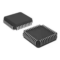
-Supplier Device Package 144-TQFP (20×20)
-Number of Gates 9000
-Voltage Supply – Internal 1.7V ~ 1.9V
-Package / Case 144-LQFP

-Number of Logic Elements/Blocks 24

Xilinx XC2C256-7CP132I -Cloud Computing -Artificial Intelligence

Xilinx XC2C256-7CP132I ApplicationField

-Medical Equipment
-Industrial Control
-5G Technology
-Internet of Things
-Wireless Technology
-Artificial Intelligence
-Consumer Electronics
-Cloud Computing

Request Xilinx XC2C256-7CP132I FPGA Quote, Pls Send Email to Sales@raypcb.com Now

Xilinx XC2C256-7CP132I FAQ

Q: How can I obtain software development tools related to the Xilinx FPGA platform?
A: In FPGA/CPLD design tools, Xilinx’s Vivado Design Suite is easy to use, it is very user-friendly in synthesis and implementation, and it is easier to use than ISE design tools; The specific choice depends on personal habits and functional requirements to specifically select a more suitable match. You can search and download through the FPGA resource channel.

Q: Does the price of XC2C256-7CP132I devices fluctuate frequently?
A: The RAYPCB search engine monitors the XC2C256-7CP132I inventory quantity and price of global electronic component suppliers in real time, and regularly records historical price data. You can view the historical price trends of electronic components to provide a basis for your purchasing decisions.

Q: Do I have to sign up on the website to make an inquiry for XC2C256-7CP132I?
A: No, only submit the quantity, email address and other contact information required for the inquiry of XC2C256-7CP132I, but you need to sign up for the post comments and resource downloads.

Q: Where can I purchase Xilinx XC2C256 Development Boards, Evaluation Boards, or CoolRunner-II CPLD Starter Kit? also provide technical information?
A: RAYPCB does not provide development board purchase services for the time being, but customers often consult about ZedBoard, Basys 3 board, TinyFPGA BX, Nexys4-DDR, Terasic DE10-Nano, Digilent Arty S7, etc. If you need relevant technical information, you can submit feedback information, our technicians will contact you soon.

Q: What should I do if I did not receive the technical support for XC2C2567CP132I in time?
A: Depending on the time difference between your location and our location, it may take several hours for us to reply, please be patient, our FPGA technical engineer will help you with the XC2C256-7CP132I pinout information, replacement, datasheet in pdf, programming tools, starter kit, etc.

Q: How to obtain XC2C256-7CP132I technical support documents?
A: Enter the “XC2C256-7CP132I” keyword in the search box of the website, or find these through the Download Channel or FPGA Forum .

Xilinx XC2C256-7CP132I Features

– 208-pin PQFP with 173 user I/O
– 144-pin TQFP with 118 user I/O
• Optimized for 1.8V systems
– 132-ball CP (0.5mm) BGA with 106 user I/O
– As low as 13 μA quiescent current

– 256-ball FT (1.0mm) BGA with 184 user I/O
– 100-pin VQFP with 80 user I/O

– As fast as 5.7 ns pin-to-pin delays
– Pb-free available for all packages
• Industry’s best 0.18 micron CMOS CPLD

• Available in multiple package options
– Optimized architecture for effective logic synthesis. Refer to the CoolRunner-II family data sheet for architecture description.

– Multi-voltage I/O operation — 1.5V to 3.3V

Request Xilinx XC2C256-7CP132I FPGA Quote, Pls Send Email to Sales@raypcb.com Now

Xilinx XC2C256-7CP132I Overview

The CoolRunner-II 128 macrocell CPLD is I/O compatible with various JEDEC I/O standards (see Table 1). This XC2C256-7CP132I device is also 1.5V I/O compatible with the use of Schmitt-trigger inputs. The XC2C256-7CP132I device is designed for both high performance and low power applications. This lends power savings to high-end communication equipment and high speed to battery operated devices. Due to the low power stand-by and dynamic operation, overall system reliability is improved
This XC2C256-7CP132I device consists of eight Function Blocks inter-connected by a low power Advanced Interconnect Matrix (AIM). The AIM feeds 40 true and complement inputs to each Function Block. The Function Blocks consist of a 40 by 56 P-term PLA and 16 macrocells which contain numerous configuration bits that allow for combinational or registered modes of operation.
Additionally, these registers can be globally reset or preset and configured as a D or T flip-flop or as a D latch. There are also multiple clock signals, both global and local product term types, configured on a per macrocell basis. Output pin configurations include slew rate limit, bus hold, pull-up, open drain and programmable grounds. A Schmitt-trigger input is available on a per input pin basis. In addition to storing macrocell output states, the macrocell registers may be configured as direct input registers to store signals directly from input pins.
Clocking is available on a global or Function Block basis. Three global clocks are available for all Function Blocks as a synchronous clock source. Macrocell registers can be individually configured to power up to the zero or one state. A global set/reset control line is also available to asynchronously set or reset selected registers during operation. Additional local clock, synchronous clock-enable, asynchronous set/reset and output enable signals can be formed using product terms on a per-macrocell or per-Function Block basis.
A DualEDGE flip-flop feature is also available on a per macrocell basis. This feature allows high performance synchronous operation based on lower frequency clocking to help reduce the total power consumption of the XC2C256-7CP132I device.
Circuitry has also been included to divide one externally supplied global clock (GCK2) by eight different selections. This yields divide by even and odd clock frequencies.
The use of the clock divide (division by 2) and DualEDGE flip-flop gives the resultant CoolCLOCK feature
DataGATE is a method to selectively disable inputs of the CPLD that are not of interest during certain points in time.
By mapping a signal to the DataGATE function, lower power can be achieved due to reduction in signal switching.
Another feature that eases voltage translation is I/O banking. Two I/O banks are available on the XC2C256-7CP132I device that permit easy interfacing to 3.3V, 2.5V, 1.8V, and 1.5V devices.
The Xilinx CPLDs series XC2C256-7CP132I is 256 MACROCELL 1.8V ZERO POWER ISP CPLD, View Substitutes & Alternatives along with datasheets, stock, pricing from Authorized Distributors at RAYPCB.com,
and you can also search for other FPGAs products.

Xilinx XC2C256-7CP132I Tags

1. Xilinx CoolRunner-II CPLD development board
2. XC2C256 reference design
3. CoolRunner-II CPLD starter kit
4. XC2C256 development board
5. CoolRunner-II CPLD XC2C256
6. XC2C256 evaluation board
7. XC2C256-7CP132I Datasheet PDF
8. CoolRunner-II CPLD evaluation kit
9. XC2C256 development board

Xilinx XC2C256-7CP132I TechnicalAttributes

-Number of Logic Elements/Blocks 16
-Voltage Supply – Internal 1.7V ~ 1.9V
-Number of Macrocells 256
-Programmable Type In System Programmable
-Delay Time tpd(1) Max 6.7ns
-Number of Gates 6000
-Package / Case 132-TFBGA, CSPBGA
-Mounting Type Surface Mount
-Operating Temperature -40โ„ƒ ~ 85โ„ƒ (TA)
-Number of I/O 106

-Supplier Device Package 132-CSPBGA (8×8)

Xilinx FPGA Programming Guide: JTAG, SPI Flash, and Vivado Tools for Spartan 6 & Zynq

Xilinx FPGA Programming

Field-Programmable Gate Arrays (FPGAs) have revolutionized the world of digital circuit design, offering unprecedented flexibility and performance. Among the leading FPGA manufacturers, Xilinx stands out with its cutting-edge devices and robust development ecosystem. This comprehensive guide delves into the intricacies of Xilinx FPGA programming, focusing on popular families like Spartan 6 and Zynq, while exploring essential programming methods and tools.

Understanding Xilinx FPGA Architecture

Before diving into programming techniques, it’s crucial to grasp the fundamental architecture of Xilinx FPGAs. This understanding forms the foundation for effective FPGA design and implementation.

Basic Building Blocks

Xilinx FPGAs consist of several key components:

  1. Configurable Logic Blocks (CLBs): These are the primary logic resources in Xilinx FPGAs, containing Look-Up Tables (LUTs) and flip-flops for implementing combinational and sequential logic.
  2. Input/Output Blocks (IOBs): These blocks interface the FPGA with external devices, supporting various I/O standards.
  3. Block RAM (BRAM): Dedicated memory blocks that provide high-speed, on-chip storage.
  4. DSP Slices: Specialized blocks for efficient implementation of digital signal processing functions.
  5. Clock Management Tiles: These blocks handle clock distribution and generation within the FPGA.

Spartan 6 vs. Zynq Architecture

While both Spartan 6 and Zynq families are Xilinx products, they have distinct architectural differences:

  • Spartan 6: A cost-effective FPGA family designed for high-volume applications. It features a balance of low power consumption and high performance.
  • Zynq: An advanced system-on-chip (SoC) platform that combines a dual-core ARM Cortex-A9 processor with FPGA fabric, offering a versatile solution for complex embedded systems.

Understanding these architectural nuances is crucial for optimizing your FPGA designs and choosing the right platform for your project.

Xilinx FPGA Programming Methods

Xilinx FPGAs support various programming methods, each with its own advantages and use cases. Let’s explore the two most common methods: JTAG and SPI Flash.

JTAG Programming

JTAG (Joint Test Action Group) is a widely used method for programming and debugging Xilinx FPGAs.

How JTAG Works

  1. JTAG uses a standardized interface (IEEE 1149.1) for testing and programming integrated circuits.
  2. It requires a JTAG programmer or a development board with built-in JTAG circuitry.
  3. The JTAG interface typically consists of four signals: TDI (Test Data In), TDO (Test Data Out), TCK (Test Clock), and TMS (Test Mode Select).

Advantages of JTAG Programming

  • Direct and interactive debugging capabilities
  • Supports in-system programming
  • Allows for real-time monitoring of FPGA internals

JTAG Programming Process

  1. Connect the JTAG programmer to your computer and the FPGA board.
  2. Use Xilinx tools (e.g., iMPACT or Vivado) to detect the FPGA device.
  3. Load the bitstream file (.bit) generated from your design.
  4. Program the FPGA directly through the JTAG interface.

SPI Flash Programming

SPI (Serial Peripheral Interface) Flash programming is another popular method, especially for designs that require non-volatile storage of configuration data.

How SPI Flash Programming Works

  1. The bitstream is stored in an external SPI Flash memory.
  2. On power-up or reset, the FPGA loads the configuration from the SPI Flash.
  3. This method allows for persistent programming, even after power cycles.

Advantages of SPI Flash Programming

  • Enables automatic configuration on power-up
  • Suitable for standalone applications
  • Allows for larger bitstream storage compared to some on-chip options

SPI Flash Programming Process

  1. Generate a .mcs or .bin file from your bitstream using Xilinx tools.
  2. Use a Flash programmer or the FPGA itself to program the SPI Flash memory.
  3. Configure the FPGA to load from SPI Flash on startup.

Vivado Design Suite: The Heart of Xilinx FPGA Programming

Xilinx’s Vivado Design Suite is a powerful integrated development environment (IDE) for FPGA programming. It offers a comprehensive set of tools for design, synthesis, implementation, and verification of FPGA projects.

Key Features of Vivado

  1. Integrated Design Environment: Vivado provides a unified workspace for all stages of FPGA development.
  2. High-Level Synthesis: Enables C, C++, and SystemC code to be directly synthesized into FPGA hardware.
  3. IP Integrator: Allows for easy integration of pre-designed IP cores into your project.
  4. Advanced Timing and Power Analysis: Offers sophisticated tools for optimizing performance and power consumption.
  5. Hardware Debug: Provides in-system debugging capabilities for real-time analysis.

Vivado Design Flow

Understanding the Vivado design flow is crucial for efficient FPGA programming:

  1. Project Creation: Start by creating a new project and specifying the target FPGA device.
  2. Design Entry: This can be done using Hardware Description Languages (HDL) like VHDL or Verilog, or through schematic entry.
  3. Behavioral Simulation: Verify the logical correctness of your design through simulation.
  4. Synthesis: Convert your HDL code into a gate-level netlist.
  5. Implementation:
    • Translate: Convert the netlist into a format compatible with the target FPGA.
    • Map: Fit the design into the available FPGA resources.
    • Place and Route: Determine the optimal placement of logic elements and routing connections.
  6. Timing Analysis: Ensure that your design meets timing constraints.
  7. Bitstream Generation: Create the final configuration file for programming the FPGA.
  8. Device Programming: Load the bitstream onto the FPGA using JTAG or program it into SPI Flash.

Tips for Effective Vivado Usage

  • Utilize Vivado’s built-in documentation and tutorials for learning new features.
  • Make use of Tcl scripting for automating repetitive tasks.
  • Regularly save your work and use version control for managing design iterations.
  • Leverage Vivado’s report generation features for design analysis and optimization.

Read more about:

FPGA Programming Best Practices

To ensure successful Xilinx FPGA programming, consider the following best practices:

Design Considerations

  1. Modular Design: Break your project into manageable modules for easier debugging and maintenance.
  2. Synchronous Design: Use synchronous logic to minimize timing issues and improve reliability.
  3. Clock Domain Crossing: Carefully handle signals that cross between different clock domains to avoid metastability issues.
  4. Resource Utilization: Be mindful of FPGA resource usage to avoid over-utilization and routing congestion.

Optimization Techniques

  1. Pipelining: Insert pipeline stages to improve throughput in high-speed designs.
  2. Retiming: Optimize the placement of registers to balance timing across logic stages.
  3. Resource Sharing: Identify opportunities to share resources for operations that don’t need to occur simultaneously.
  4. Constraint-Driven Design: Use timing and placement constraints to guide the tools for optimal results.

Debugging and Verification

  1. Simulation: Thoroughly simulate your design at multiple levels (behavioral, post-synthesis, post-implementation).
  2. In-System Debugging: Utilize Vivado’s Integrated Logic Analyzer (ILA) for real-time hardware debugging.
  3. Formal Verification: Consider using formal methods to prove the correctness of critical design components.

Advanced Topics in Xilinx FPGA Programming

As you gain proficiency in Xilinx FPGA programming, exploring advanced topics can significantly enhance your designs and productivity.

Partial Reconfiguration

Partial Reconfiguration (PR) allows you to modify portions of the FPGA design while the rest of the device continues to operate. This feature is particularly useful in applications requiring adaptive hardware or time-sharing of FPGA resources.

Benefits of Partial Reconfiguration:

  • Improved resource utilization
  • Enhanced system flexibility
  • Reduced power consumption
  • Ability to update designs in the field

Implementing Partial Reconfiguration:

  1. Identify reconfigurable regions in your design.
  2. Create multiple configurations for these regions.
  3. Use Vivado’s PR flow to generate partial bitstreams.
  4. Implement a mechanism to load these partial bitstreams during runtime.

High-Level Synthesis

Xilinx’s High-Level Synthesis (HLS) tool allows developers to create FPGA designs using high-level languages like C, C++, and SystemC. This approach can significantly reduce development time and make FPGA programming more accessible to software engineers.

Advantages of HLS:

  • Faster development cycle
  • Easier algorithm implementation
  • Simplified design space exploration
  • Improved code reusability

HLS Design Flow:

  1. Write your algorithm in C/C++/SystemC.
  2. Use pragmas and directives to guide the HLS tool.
  3. Synthesize the high-level code into RTL.
  4. Integrate the generated RTL into your Vivado project.

FPGA-Based Acceleration

With the increasing demand for high-performance computing, FPGAs are becoming popular for accelerating computationally intensive tasks. Xilinx offers solutions like Vitis for creating accelerated applications.

Applications of FPGA Acceleration:

  • Machine Learning inference
  • Video processing
  • Financial analytics
  • Genomics research

Implementing FPGA Acceleration:

  1. Identify computationally intensive parts of your application.
  2. Design custom hardware accelerators using HLS or HDL.
  3. Use Xilinx Runtime (XRT) for managing the accelerators.
  4. Integrate the FPGA acceleration with your host application.

Xilinx FPGA Programming for Specific Applications

Different applications have unique requirements and considerations when it comes to FPGA programming. Let’s explore some specific areas where Xilinx FPGAs excel.

Digital Signal Processing (DSP)

Xilinx FPGAs are widely used in DSP applications due to their dedicated DSP slices and flexible architecture.

Key Considerations for DSP on FPGAs:

  • Utilize DSP48 slices for efficient implementation of mathematical operations.
  • Implement proper pipelining to achieve high throughput.
  • Consider fixed-point arithmetic for resource-efficient designs.
  • Use Xilinx DSP IP cores for common functions like FFTs and FIR filters.

Embedded Systems with Zynq

The Zynq family, with its integrated ARM processors, is ideal for embedded systems that require both software flexibility and hardware acceleration.

Tips for Zynq-based Designs:

  • Partition your application between the Processing System (PS) and Programmable Logic (PL).
  • Use AXI interfaces for efficient communication between PS and PL.
  • Leverage Xilinx SDK for software development on the ARM cores.
  • Consider using FreeRTOS or Linux for complex embedded applications.

High-Speed Networking

Xilinx FPGAs are often used in networking equipment for their ability to handle high-speed data processing and packet manipulation.

Networking Design Strategies:

  • Utilize multi-gigabit transceivers for high-speed data interfaces.
  • Implement efficient packet parsing and forwarding logic.
  • Consider using Xilinx’s networking IP cores for standard protocols.
  • Optimize for low latency in time-critical applications.

Future Trends in Xilinx FPGA Programming

As technology evolves, so does the field of FPGA programming. Stay ahead of the curve by keeping an eye on these emerging trends:

  1. AI and Machine Learning: Xilinx is increasingly focusing on AI acceleration, with tools and architectures optimized for machine learning workloads.
  2. Adaptive Computing: The concept of adaptive computing, where hardware can dynamically reconfigure based on workload, is gaining traction.
  3. Higher Level Abstractions: Expect more tools and methodologies that allow programming FPGAs at higher levels of abstraction, making them accessible to a broader range of developers.
  4. Integration with Cloud Services: FPGA-as-a-Service offerings are becoming more prevalent, allowing for cloud-based FPGA development and deployment.
  5. Open-Source Tools: The growth of open-source FPGA tools may influence how Xilinx and other vendors approach their toolchains.

Conclusion

Xilinx FPGA programming offers a vast landscape of possibilities for digital design. From the versatile Spartan 6 to the powerful Zynq SoCs, Xilinx provides a range of solutions to meet diverse application needs. By mastering programming methods like JTAG and SPI Flash, leveraging the capabilities of the Vivado Design Suite, and staying abreast of advanced topics and future trends, you can unlock the full potential of Xilinx FPGAs in your projects.

Remember, FPGA programming is as much an art as it is a science. It requires creativity, problem-solving skills, and a deep understanding of digital design principles. As you continue your journey in Xilinx FPGA programming, always strive to learn, experiment, and push the boundaries of what’s possible with these remarkable devices.

Whether you’re developing high-speed networking equipment, implementing complex DSP algorithms, or creating cutting-edge embedded systems, Xilinx FPGAs provide the flexibility and performance to bring your ideas to life. Embrace the challenges, stay curious, and enjoy the process of turning your digital designs into reality with Xilinx FPGA programming.

Xilinx Artix-7 FPGA: Comprehensive Guide to XC7A100T, XC7A35T, and XC7A200T for Cost-Sensitive Designs

Xilinx Artix-7 FPGA

In the ever-evolving landscape of digital design, Field-Programmable Gate Arrays (FPGAs) have become indispensable tools for engineers and designers seeking flexibility, performance, and cost-effectiveness. Among the various FPGA families available, the Xilinx Artix-7 series stands out as a popular choice for cost-sensitive applications that still demand significant processing power. This comprehensive guide delves into the Xilinx Artix-7 FPGA family, with a particular focus on three key models: the XC7A100T, XC7A35T, and XC7A200T.

Understanding the Xilinx Artix-7 FPGA Family

Before we dive into the specific models, it’s crucial to understand what makes the Xilinx Artix-7 FPGA family unique and why it’s an excellent choice for cost-sensitive designs.

Key Features of Xilinx Artix-7 FPGAs

  1. Low Power Consumption: Artix-7 FPGAs are designed for power efficiency, making them ideal for battery-powered and energy-conscious applications.
  2. High Performance: Despite their focus on cost-effectiveness, Artix-7 FPGAs offer impressive performance capabilities.
  3. Scalability: The family includes a range of devices with varying resource counts, allowing designers to choose the right fit for their application.
  4. Advanced Process Technology: Built on 28nm process technology, ensuring a good balance of performance and power efficiency.
  5. Rich I/O Capabilities: Supports a wide range of I/O standards and protocols.
  6. Integrated Block RAM: On-chip memory for fast data access and processing.
  7. DSP Slices: Dedicated digital signal processing blocks for efficient implementation of arithmetic operations.

Benefits of Choosing Xilinx Artix-7 for Cost-Sensitive Designs

  • Cost-Effectiveness: Offers a balance of performance and price, suitable for budget-conscious projects.
  • Power Efficiency: Lower power consumption leads to reduced cooling requirements and longer battery life in portable applications.
  • Flexibility: Reprogrammable nature allows for design iterations and updates without hardware changes.
  • Time-to-Market: Rapid prototyping and development capabilities accelerate product launch timelines.
  • Ecosystem Support: Extensive tools, IP cores, and community support from Xilinx and third-party providers.

Xilinx Artix-7 XC7A100T: The Versatile Performer

The XC7A100T is a popular model in the Artix-7 family, offering a balanced mix of resources suitable for a wide range of applications.

XC7A100T Key Specifications

  • Logic Cells: 101,440
  • CLB Slices: 15,850
  • Block RAM: 4,860 Kb
  • DSP Slices: 240
  • I/O Pins: Up to 300
  • Transceivers: Up to 16 (6.6 Gb/s)

XC7A100T Performance Highlights

  1. Logic Performance: Capable of implementing complex logic functions and state machines efficiently.
  2. Memory Bandwidth: Substantial on-chip memory for data-intensive applications.
  3. DSP Capabilities: Suitable for signal processing and arithmetic-heavy designs.
  4. I/O Flexibility: Supports various I/O standards for interfacing with different peripherals and systems.

XC7A100T Use Cases

  • Industrial Automation: Control systems and motor control applications
  • Video Processing: Image filtering and basic video encoding/decoding
  • Software-Defined Radio: Flexible radio systems for various communication protocols
  • Educational Platforms: Advanced FPGA development kits for universities and training programs

XC7A100T Pricing

As of 2023, the XC7A100T is priced in the range of 100to100to200 for single unit quantities, depending on the specific package and speed grade. Volume pricing can be significantly lower and should be obtained directly from Xilinx or authorized distributors.

Read more about:

Xilinx Artix-7 XC7A35T: The Compact Powerhouse

The XC7A35T is the smallest device in our comparison, offering an excellent balance of capabilities for space-constrained and highly cost-sensitive applications.

XC7A35T Key Specifications

  • Logic Cells: 33,280
  • CLB Slices: 5,200
  • Block RAM: 1,800 Kb
  • DSP Slices: 90
  • I/O Pins: Up to 250
  • Transceivers: Up to 4 (6.6 Gb/s)

XC7A35T Performance Highlights

  1. Compact Design: Ideal for space-constrained applications without sacrificing essential FPGA capabilities.
  2. Power Efficiency: Lower resource count translates to reduced power consumption.
  3. Cost-Effectiveness: The most budget-friendly option in our comparison.
  4. Sufficient I/O: Despite its smaller size, it still offers a generous number of I/O pins.

XC7A35T Use Cases

  • IoT Devices: Edge computing and sensor fusion in Internet of Things applications
  • Consumer Electronics: Digital signal processing in audio equipment or smart home devices
  • Medical Devices: Portable medical equipment requiring low power consumption
  • Automotive: In-vehicle infotainment systems and basic ADAS (Advanced Driver-Assistance Systems) functions

XC7A35T Pricing

The XC7A35T is typically priced between 50and50and100 for single unit quantities, making it an attractive option for cost-sensitive designs. As always, volume pricing can offer significant discounts.

Xilinx Artix-7 XC7A200T: The Resource-Rich Powerhouse

The XC7A200T represents the high end of the Artix-7 family, offering the most resources for designers who need maximum performance within the Artix-7 ecosystem.

XC7A200T Key Specifications

  • Logic Cells: 215,360
  • CLB Slices: 33,650
  • Block RAM: 13,140 Kb
  • DSP Slices: 740
  • I/O Pins: Up to 500
  • Transceivers: Up to 16 (6.6 Gb/s)

XC7A200T Performance Highlights

  1. High Logic Density: Capable of implementing very complex designs and multiple subsystems on a single chip.
  2. Extensive Memory Resources: Large on-chip memory capacity for data-intensive applications.
  3. Powerful DSP Capabilities: Ideal for complex signal processing and arithmetic operations.
  4. Rich I/O Resources: Supports interfacing with multiple high-speed peripherals simultaneously.

XC7A200T Use Cases

  • High-Performance Computing: Data processing and acceleration for scientific applications
  • Advanced Image Processing: Real-time video analytics and computer vision systems
  • 5G Infrastructure: Baseband processing and network packet processing
  • AI and Machine Learning: Implementation of neural network accelerators and inference engines

XC7A200T Pricing

The XC7A200T, being the most capable device in our comparison, is typically priced between 300and300and500 for single unit quantities. As with other models, volume pricing can offer substantial discounts.

Performance Comparison: XC7A100T vs XC7A35T vs XC7A200T

To better understand how these Xilinx Artix-7 FPGA models compare, let’s look at a side-by-side comparison of their key performance metrics:

FeatureXC7A100TXC7A35TXC7A200T
Logic Cells101,44033,280215,360
CLB Slices15,8505,20033,650
Block RAM4,860 Kb1,800 Kb13,140 Kb
DSP Slices24090740
Max I/O Pins300250500
TransceiversUp to 16Up to 4Up to 16
Relative CostMediumLowHigh

Key Takeaways from the Comparison

  1. Scalability: The Artix-7 family offers a wide range of resource options to fit various project requirements.
  2. Memory Scaling: Block RAM increases significantly with device size, benefiting data-intensive applications.
  3. DSP Resources: The XC7A200T offers substantially more DSP slices, making it ideal for compute-heavy designs.
  4. I/O Flexibility: Even the smallest device (XC7A35T) offers ample I/O pins for most applications.
  5. Cost Considerations: There’s a clear trade-off between resources and cost across the three models.

Designing with Xilinx Artix-7 FPGAs

Successful implementation of cost-sensitive designs using Xilinx Artix-7 FPGAs requires careful consideration of several factors:

1. Resource Utilization

  • Logic Optimization: Efficient use of logic cells and CLB slices is crucial for maximizing design capabilities.
  • Memory Management: Proper allocation of block RAM can significantly impact performance and power consumption.
  • DSP Usage: Leveraging DSP slices for arithmetic operations can improve both performance and power efficiency.

2. Power Management

  • Dynamic Power Reduction: Techniques like clock gating and power gating can reduce dynamic power consumption.
  • Static Power Considerations: Choosing the right speed grade and package can help minimize static power draw.
  • Thermal Management: Proper thermal design is essential, especially for the larger XC7A200T in high-performance applications.

3. I/O Planning

  • Pin Assignment: Careful planning of I/O pin assignments can simplify PCB layout and improve signal integrity.
  • I/O Standards: Selecting the appropriate I/O standards for interfacing with other components is crucial for system compatibility.

4. Timing Closure

  • Constraints Management: Proper definition and management of timing constraints are essential for achieving desired performance.
  • Clock Domain Crossing: Careful handling of signals crossing clock domains is crucial for reliable operation.

5. Cost Optimization

  • Device Selection: Choosing the right Artix-7 model that meets performance requirements without overprovisioning.
  • External Component Reduction: Leveraging FPGA resources to integrate functions that might otherwise require external components.

Development Tools and Ecosystem

Xilinx provides a comprehensive suite of tools and a rich ecosystem to support Artix-7 FPGA development:

Vivado Design Suite

The primary development environment for Artix-7 FPGAs, offering:

  1. High-Level Synthesis: Allows design implementation using C, C++, or SystemC.
  2. IP Integrator: Graphical environment for IP-based design.
  3. Simulation and Debugging Tools: Comprehensive verification capabilities.

Vitis Unified Software Platform

While primarily targeted at Xilinx’s more advanced FPGAs, parts of the Vitis platform can be useful for Artix-7 development:

  1. Vitis HLS: High-level synthesis tool for creating hardware from C/C++ code.
  2. Vitis Libraries: Optimized libraries for various functions and algorithms.

Third-Party Tools and IP

The Xilinx ecosystem includes support for various third-party tools and IP cores:

  1. MATLAB and Simulink: Support for model-based design and automatic code generation.
  2. QuestaSim and ModelSim: Popular simulation tools compatible with Xilinx designs.
  3. Third-Party IP Cores: Wide range of pre-designed IP cores available for accelerating development.

Real-World Success Stories

To illustrate the impact of Xilinx Artix-7 FPGAs in cost-sensitive designs, let’s look at some real-world applications and success stories:

Case Study 1: Industrial Control System

A manufacturer of industrial automation equipment used the XC7A100T to develop a new generation of programmable logic controllers (PLCs):

  • 40% reduction in overall system cost compared to their previous ASIC-based solution
  • 3x improvement in I/O response time
  • Ability to update control algorithms in the field, improving product longevity

Case Study 2: Portable Medical Device

A medical device startup leveraged the XC7A35T in a wearable ECG monitor:

  • 50% reduction in power consumption compared to their initial microcontroller-based design
  • Real-time implementation of complex ECG analysis algorithms
  • Achieved medical-grade accuracy in a compact, cost-effective form factor

Case Study 3: 5G Network Equipment

A telecommunications equipment manufacturer used the XC7A200T in their 5G small cell base station design:

  • 70% reduction in bill of materials compared to using multiple discrete components
  • Flexible support for multiple 5G standards through firmware updates
  • Improved spectral efficiency through advanced signal processing algorithms

Future Outlook for Xilinx Artix-7 FPGAs

While the Artix-7 family has been a staple in cost-sensitive FPGA designs for several years, it’s important to consider its future in the rapidly evolving world of programmable logic:

Continued Relevance

  1. Established Ecosystem: The mature development ecosystem and wide availability of IP cores ensure ongoing relevance.
  2. Cost-Effectiveness: As newer FPGA families emerge, Artix-7 may become even more cost-effective for certain applications.
  3. Known Reliability: With years of field deployment, Artix-7 FPGAs have proven their reliability in various environments.

Emerging Applications

  1. Edge AI: As AI moves to the edge, Artix-7 FPGAs could find new roles in implementing lightweight inference engines.
  2. IoT Gateways: The balance of performance and power efficiency makes Artix-7 suitable for IoT gateway applications.
  3. Legacy System Integration: Artix-7 FPGAs can serve as bridges between modern systems and legacy interfaces.

Technology Trends

While specific details of future Xilinx (now part of AMD) plans are not public, we can anticipate:

  1. Software Tool Enhancements: Continued improvements in development tools to simplify FPGA design and optimization.
  2. IP Ecosystem Growth: Expansion of available IP cores, especially in emerging application areas.
  3. Integration with Newer Xilinx Families: Potential for mixed-technology designs combining Artix-7 with newer Xilinx FPGAs.

Conclusion: The Enduring Value of Xilinx Artix-7 FPGAs

The Xilinx Artix-7 FPGA family, particularly the XC7A100T, XC7A35T, and XC7A200T models, continues to offer compelling value for cost-sensitive designs across a wide range of applications. By providing a balance of performance, power efficiency, and cost-effectiveness, these FPGAs enable innovative solutions in industries ranging from industrial automation to medical devices and telecommunications.

Key takeaways for designers considering Xilinx Artix-7 FPGAs:

  1. Scalability: The range from XC7A35T to XC7A200T offers flexibility in choosing the right balance of resources and cost.
  2. Performance: Despite their focus on cost-sensitivity, Artix-7 FPGAs deliver impressive performance for many applications.
  3. Power Efficiency: Low power consumption makes them suitable for battery-powered and energy-conscious designs.
  4. Ecosystem Support: A mature development environment and rich IP ecosystem accelerate time-to-market.
  5. Future-Proofing: The reprogrammable nature of FPGAs allows for field updates and adaptation to evolving requirements.

As we look to the future, the Xilinx Artix-7 family is likely to remain a go-to solution for many cost-sensitive designs. While newer FPGA families may offer higher performance or more advanced features, the Artix-7’s combination of cost-effectiveness, proven reliability, and comprehensive ecosystem support ensures its continued relevance in many application areas.

For engineers and project managers working on cost-sensitive designs, the decision to use an Artix-7 FPGA should be based on a careful evaluation of project requirements, including:

  • Performance needs
  • Power constraints
  • Budget limitations
  • Time-to-market pressures
  • Long-term maintenance and upgrade considerations

By carefully matching these requirements to the capabilities of the XC7A100T, XC7A35T, or XC7A200T, designers can leverage the power of FPGA technology while maintaining cost-effectiveness. This approach can lead to innovative solutions that balance performance, power efficiency, and cost in ways that may not be possible with other technologies.

In conclusion, the Xilinx Artix-7 FPGA family represents a versatile and powerful tool in the designer’s arsenal for cost-sensitive applications. Whether you’re developing industrial control systems, medical devices, telecommunications equipment, or exploring new frontiers in IoT and edge computing, the Artix-7 offers a compelling combination of features that can help bring your ideas to life without breaking the bank. As the digital landscape continues to evolve, the flexibility and cost-effectiveness of Artix-7 FPGAs are likely to ensure their place in the world of electronic design for years to come.

Xilinx Kintex-7 FPGA: Comprehensive Guide to XC7K325T, XC7K160T, and XC7K410T for High-Performance Designs

xilinx kintex 7 FPGA

In the ever-evolving world of digital electronics, Field-Programmable Gate Arrays (FPGAs) have become indispensable tools for designers seeking flexibility, performance, and efficiency. Among the various FPGA families available, the Xilinx Kintex-7 series stands out as a powerful and versatile option for a wide range of applications. This comprehensive guide delves into the Kintex-7 FPGA family, with a particular focus on three popular models: the XC7K325T, XC7K160T, and XC7K410T. We’ll explore their features, applications, and how they can be leveraged to create high-performance designs.

Understanding the Xilinx Kintex-7 FPGA Family

The Kintex-7 FPGA family, introduced by Xilinx, represents a significant advancement in FPGA technology. These devices are designed to deliver high performance and power efficiency, making them ideal for a variety of applications ranging from communications infrastructure to high-end consumer products.

Key Features of Kintex-7 FPGAs

  1. 28nm HPL (High-Performance, Low-Power) process technology
  2. High-performance DSP slices for efficient signal processing
  3. Flexible memory options, including block RAM and distributed RAM
  4. Advanced clocking technology with low-jitter clock management
  5. High-speed serial transceivers for efficient data transfer
  6. Reduced power consumption compared to previous generations

The Kintex-7 Advantage

Kintex-7 FPGAs offer a balance between performance and cost, positioning themselves as an excellent choice for designers who need more capabilities than entry-level FPGAs but don’t require the extreme performance of high-end devices. This makes them particularly attractive for applications in telecommunications, medical imaging, and industrial automation.

Deep Dive into XC7K325T, XC7K160T, and XC7K410T

Now, let’s examine the three specific Kintex-7 models that are widely used in high-performance designs: the XC7K325T, XC7K160T, and XC7K410T.

XC7K325T: Balanced Performance and Resources

The XC7K325T is a popular choice among designers for its well-balanced combination of logic resources, memory, and I/O capabilities.

Key Specifications:

  • Logic Cells: 326,080
  • CLB Flip-Flops: 407,600
  • CLB LUTs: 203,800
  • Block RAM: 16,020 Kb
  • DSP Slices: 840
  • SelectIO pins: 500
  • Transceiver Count: 16

Applications:

The XC7K325T is well-suited for applications such as:

  1. Advanced driver assistance systems (ADAS)
  2. Medical imaging equipment
  3. High-performance computing
  4. Wireless infrastructure

XC7K160T: Compact Yet Powerful

The XC7K160T offers a more compact solution while still providing substantial resources for complex designs.

Key Specifications:

  • Logic Cells: 162,240
  • CLB Flip-Flops: 202,800
  • CLB LUTs: 101,400
  • Block RAM: 11,700 Kb
  • DSP Slices: 600
  • SelectIO pins: 400
  • Transceiver Count: 8

Applications:

The XC7K160T is ideal for:

  1. Industrial automation systems
  2. Video processing applications
  3. Software-defined radio
  4. Network security appliances

XC7K410T: High-End Performance

For designs requiring maximum resources and performance, the XC7K410T stands at the top of the Kintex-7 lineup.

Key Specifications:

  • Logic Cells: 406,720
  • CLB Flip-Flops: 508,400
  • CLB LUTs: 254,200
  • Block RAM: 28,620 Kb
  • DSP Slices: 1,540
  • SelectIO pins: 500
  • Transceiver Count: 16

Applications:

The XC7K410T is perfect for demanding applications such as:

  1. High-frequency trading systems
  2. Advanced radar and sonar processing
  3. Large-scale data centers
  4. 5G base stations

Read more about:

Leveraging Kintex-7 FPGAs for High-Performance Designs

Now that we’ve explored the specifications of these Kintex-7 models, let’s discuss how to leverage their capabilities for high-performance designs.

Optimizing DSP Performance

Kintex-7 FPGAs feature advanced DSP slices that can significantly boost signal processing performance. To make the most of these resources:

  1. Utilize DSP inference in your HDL code to ensure efficient mapping to DSP slices
  2. Consider using Xilinx’s DSP IP cores for complex operations like FFTs and FIR filters
  3. Implement pipelining to achieve higher clock frequencies and throughput

Efficient Memory Utilization

The Kintex-7 family offers various memory options, including block RAM and distributed RAM. To optimize memory usage:

  1. Use block RAM for larger data storage requirements
  2. Leverage distributed RAM for smaller, faster memory needs
  3. Implement proper memory partitioning to avoid bottlenecks
  4. Utilize Xilinx’s memory interface solutions for external memory connections

High-Speed I/O and Connectivity

The high-speed transceivers in Kintex-7 FPGAs enable efficient data transfer. To maximize their potential:

  1. Implement proper signal integrity techniques for high-speed designs
  2. Utilize Xilinx’s SelectIO technology for flexible I/O configurations
  3. Consider using PCIe interfaces for high-bandwidth connectivity with host systems

Power Optimization Techniques

While Kintex-7 FPGAs are inherently power-efficient, further optimizations can be achieved:

  1. Utilize clock gating to reduce dynamic power consumption
  2. Implement power-aware placement and routing strategies
  3. Use Xilinx’s Power Optimization tool to identify areas for improvement

Design Tools and Development Environment

Xilinx Kintex fpga
Xilinx Kintex fpga

To effectively design with Kintex-7 FPGAs, it’s crucial to use the right tools and development environment.

Xilinx Vivado Design Suite

The primary development environment for Kintex-7 FPGAs is the Xilinx Vivado Design Suite. Key features include:

  1. High-level synthesis for C/C++ to RTL conversion
  2. Advanced timing analysis and optimization tools
  3. Integrated logic analyzer for on-chip debugging
  4. Power analysis and optimization capabilities

IP Cores and Reference Designs

Xilinx provides a wealth of IP cores and reference designs that can accelerate development with Kintex-7 FPGAs:

  1. DSP IP cores for signal processing applications
  2. Communication protocol cores (Ethernet, PCIe, etc.)
  3. Memory interface solutions
  4. Video and image processing IP

Third-Party Tools and Ecosystem

A robust ecosystem of third-party tools and IP providers further enhances the Kintex-7 design experience:

  1. High-level synthesis tools from vendors like Mentor Graphics and Cadence
  2. Specialized IP cores for specific applications
  3. System-level design and verification tools

Real-World Applications and Case Studies

To better understand the capabilities of Kintex-7 FPGAs, let’s explore some real-world applications and case studies.

Case Study 1: 5G Base Station Design

A telecommunications company utilized the XC7K410T to develop a high-performance 5G base station. The abundant DSP resources allowed for efficient implementation of complex signal processing algorithms, while the high-speed transceivers enabled rapid data transfer between different system components.

Case Study 2: Medical Imaging Equipment

A medical device manufacturer leveraged the XC7K325T for a new generation of MRI scanners. The FPGA’s balanced resources allowed for real-time image processing and data acquisition, significantly improving image quality and reducing scan times.

Case Study 3: Industrial Automation

An industrial automation company used the XC7K160T to create a versatile control system for manufacturing plants. The FPGA’s compact size and ample resources enabled the implementation of complex control algorithms and multiple communication interfaces in a single device.

Future Trends and Developments

As technology continues to evolve, the role of FPGAs like the Kintex-7 series is likely to expand. Some future trends to watch include:

  1. Increased integration of AI and machine learning capabilities
  2. Enhanced support for edge computing applications
  3. Further improvements in power efficiency and performance
  4. Greater emphasis on security features and encryption

Conclusion

The Xilinx Kintex-7 FPGA family, particularly the XC7K325T, XC7K160T, and XC7K410T models, offers a powerful and flexible platform for high-performance designs across various industries. By understanding the unique features and capabilities of these devices, designers can leverage their potential to create innovative solutions that meet the demands of today’s complex applications.

Whether you’re working on telecommunications infrastructure, medical devices, industrial automation, or any other high-performance application, the Kintex-7 FPGA family provides the resources, performance, and efficiency needed to bring your designs to life. As the world of digital electronics continues to evolve, the Kintex-7 series stands ready to meet the challenges of tomorrow’s technologies.

What is Xilinx XCR3064XL-7PC44I FPGA?

Xilinx fpga chip

Introduction

The Xilinx CoolRunner-II XCR3064XL-7PC44I is a low-power CPLD (complex programmable logic device) that provides medium density, performance, and an abundance of I/O in a compact form factor. The XCR3064XL balances logic capacity with low static and dynamic power consumption, making it an excellent fit for a wide variety of embedded applications.

In this article, we will take a technical deep dive into the capabilities, architecture, and key parameters of the XCR3064XL-7PC44I to understand where it excels and how to leverage its unique characteristics. Weโ€™ll explore the datasheet specifications and discuss example usage scenarios that can benefit from this CoolRunner-II device.

XCR3064XL Overview

Here are some of the high-level features of the Xilinx XCR3064XL-7PC44I CPLD:

  • 64 macrocells providing 15,000 usable gates
  • Maximum clock speed of 350 MHz
  • 144 total user I/O pins
  • 7ns pin-to-pin delays
  • 1.2V VCCINT core supply voltage
  • 0.9W typical power consumption
  • 7 x 7 mm 144-pin TQFP package
  • Operating temperature from 0ยฐC to 85ยฐC

This provides a robust amount of logic capacity with fast performance and abundant I/Os in an efficient power envelope.

CPLD Architecture

XCR3064XL-7PC44I

The XCR3064XL architecture consists of:

  • Four sectors each containing macrocell logic blocks
  • Macrocells implement logic using product term arrays
  • Local interconnect provides intra-sector routing
  • Global interconnect enables cross-sector connectivity
  • Input/output blocks for pin routing and logic interfacing

By combining continuous interconnect with product term-based macrocells, an optimal balance of flexibility and routability is achieved.

Logic Capacity

With 64 macrocells providing 15,000 usable gates, the XCR3064XL supports reasonably complex logic designs:

  • Each macrocell contains a 32-product term lookup table (LUT) for logic implementation
  • Wide multiplexers and arithmetic carry logic expand capabilities
  • LUTs can also be split into two 16-product term functions
  • 15 inputs per macrocell simplify wide input logic
  • D-type flip-flop for registered outputs

Typical applications fit comfortably within the available logic space.

Performance

A peak internal clock speed of 350 MHz allows high speed operation:

  • Input to output delays as fast as 3.5ns
  • 7ns pin-to-pin delays available
  • Low clock-to-output delays
  • High fan-in capabilities
  • Supports source synchronous designs

The XCR3064XL provides responsive performance for time-critical embedded systems.

Power Consumption

At just 0.9W static power and 200mA peak current draw, the XCR3064XL operates efficiently:

  • 1.2V VCCINT supply voltage
  • 3.3V VCCIO for I/O interfaces
  • Low static current in mA range
  • Typical 200mW standby power
  • Suspend mode drops power to just 45mW

Power saving modes make the XCR3064XL ideal for portable and battery powered electronics.

I/O Capabilities

With 144 total user I/O pins, the CPLD supports a wide range of interfacing needs:

  • Flexible I/O banks withvoltage from 1.2V to 3.3V
  • Single-ended or differential I/O standards
  • Drive strength from 4mA to 24mA
  • PCI compliant clamp diodes
  • Programmable pull-up resistors
  • Slew rate control

Ample I/O pins reduce or eliminate external logic when interfacing with processors, buses, and peripherals.

Configuration and Security

The XCR3064XL loads configuration bitstreams from:

  • Serial peripheral interface (SPI) flash
  • Direct JTAG programming
  • Auto reconfiguration on power up
  • AES encryption secures designs

Non-volatile storage allows instant start up after loss of power. Encryption safeguards intellectual property.

Development Tools

Xilinx provides the ISE design suite for synthesizing and optimizing CPLD logic:

  • VHDL and Verilog support
  • XST synthesis tool integrates into ISE flows
  • Timing analysis identifies critical paths
  • Validate designs with ModelSim simulation
  • Xilinx programming hardware loads completed bitstreams

A full embedded development toolchain enables CPLD-based designs with the XCR3064XL.

Conclusion

With its balanced density, ample performance, low power consumption, and abundance of I/O, the Xilinx XCR3064XL-7PC44I CPLD excels at a wide array of embedded system applications. The integrated development environment makes designing with the XCR3064XL accessible for new and experienced users alike. For embeddeed systems where a full FPGA may be overkill but a small CPLD lacks sufficient capacity, the XCR3064XL hits the sweet spot.

Frequently Asked Questions

Q: What are some typical applications suitable for the XCR3064XL CPLD?

A: Example uses including motor control, IoT edge nodes, industrial automation, algorithm accelerators, instrumentation, and interface glue logic.

Q: What density CPLD should be selected if the XCR3064XL does not have sufficient capacity?

A: The larger XC95108 and XC95144/216 CPLDs provide more macrocells and I/O for more complex designs.

Q: How does the XCR3064XL compare to competing CPLDs?

A: It competes with mid-density CPLDs from Lattice, Microsemi, and other vendors, but with lower power and cost.

Q: Does the XCR3064XL support in-system programming and reconfiguration?

A: Yes, via the JTAG interface the CPLD can be reprogrammed unlimited times on the PCB.

Q: What embedded processors work well with the XCR3064XL CPLD?

A: Simple 8-bit CPUs like Microchip PIC16/18, Atmel AVR, and TI MSP430 interface easily. 32-bit ARM cores can also leverage the CPLD.

XCR3064XL-7PC44I Description

The CoolRunnerโ„ข XPLA3 XCR3064XL device is a 3.3V, 64-macrocell CPLD targeted at power sensitive designs that require leading edge programmable logic solutions. A total of four function blocks provide 1,500 usable gates. Pin-to-pin propagation delays are as fast as 5.5 ns with a maximum system frequency of 192 MHz.

ManufacturerXilinx Inc.
CategoryIntegrated Circuits (ICs) โ€“ Embedded โ€“ CPLDs (Complex Programmable Logic Devices)
Package44-LCC (J-Lead)
SeriesCoolRunner XPLA3
Programmable TypeIn System Programmable (min 1K program/erase cycles)
Delay Time tpd(1) Max7.0ns
Voltage Supply โ€“ Internal2.7 V ~ 3.6 V
Number of Logic Elements/Blocks4
Number of Macrocells64
Number of Gates1500
Number of I/O36
Operating Temperature-40ยฐC ~ 85ยฐC (TA)
Mounting TypeSurface Mount
Package / Case44-LCC (J-Lead)
Supplier Device Package44-PLCC (16.59ร—16.59)
XCR3064XL

You also could found the family series as below:

XCR3064XL-10PC44C
XCR3064XL-7PC44C
XCR3064XL-7PC44I

What is Xilinx XA3SD1800A-4CSG484Q FPGA ?

Xilinx fpga chip

Introduction

The Xilinx XA Spartan-3A Automotive (XA) FPGA family brings low-cost, reliability-optimized programmable logic to automotive applications. Within this family, the XA3SD1800A-4CSG484Q provides a balance of logic density, features, and package size suitable for body electronics, instrumentation, and engine management systems.

In this article, we will explore the key capabilities and specifications of the XA3SD1800A from its datasheet and reference manual. We’ll examine the programmable logic, hard IP blocks, I/O, reliability, and other relevant details for automotive usage.

XA3SD1800A FPGA Characteristics

XA3SD1800A-4CSG484Q

The Xilinx XA3SD1800A sits towards the higher end of the XA Spartan-3A family with these high-level characteristics:

Programmable Logic

  • 176,592 logic gates
  • 1.47 Mb block RAM
  • 20 DSP slices

I/O Count

  • 484 I/O pins
  • Support for common I/O standards

Hard IP Blocks

  • PCI Express Endpoint
  • Gigabit Ethernet MAC
  • Digital Clock Manager blocks

Package

  • 23×23 mm 484-pin fine-pitch BGA
  • Supported from -40C to +125C

This provides ample logic and routing for reasonably complex automotive applications.

FPGA Logic Cells

The core FPGA fabric that implements custom logic consists of 176,592 usable gates, organized into:

  • Configurable logic blocks (CLBs) each with 4 slices
  • Slices containing LUTs and flip-flops
  • D-type registers for pipeline stages
  • Wide multiplexers for complex logic
  • Fast carry logic for arithmetic

The FPGA fabric is built on a 150nm process optimized for automotive reliability and qualification.

Block RAM Resources

For data buffering and memory, the XA3SD1800A contains 1470 Kb of fast block RAM, organized into:

  • 65 dual-port 18 Kb blocks
  • Can be used as single port 36 Kb RAMs
  • True dual port capability with simultaneous access
  • Configurable aspect ratios for depth vs width

Block RAM enables on-chip data manipulation without external memories.

DSP Slices

For high-speed arithmetic processing, the FPGA includes 20 dedicated DSP slices, each providing:

  • 25 x 18 bit signed multiply with 48-bit accumulate
  • Optional adder feeding back into multiplier input
  • Cascading allows deeper bit precision
  • Pipelining and shifting capabilities

This enables efficient implementation of filters, fast transforms, and signal processing.

PCI Express Block

The integrated PCIe block provides a single x1 lane endpoint, with:

  • PCIe 1.1 compliant interface at 2.5 Gbps
  • Transaction layer and data link layer support
  • Supports serial transceivers up to 3.125 Gbps
  • Provides high speed interconnect without consuming FPGA resources

Gigabit Ethernet Blocks

Two Ethernet MAC blocks support 10/100/1000 Mbps operation with:

  • 1500 byte jumbo frame support
  • Simplex, duplex, and autonegotiation modes
  • RGMII interface to external PHY
  • Scatter-gather DMA
  • Statistics counter registers

Clock Management

Six digital clock managers (DCMs) provide:

  • Input clock synthesis up to 500 MHz
  • Zero-delay buffering on clock nets
  • Precision clock deskew, division, and phase alignment

Multiple low-skew global clock networks distribute and route clocks to logic areas with precise matching.

XA3SD1800A Packaging

The XA3SD1800A is available in FCBGA484 package:

  • 23x23mm body, 1mm ball pitch
  • Supported -40C to +125C temperature range
  • Pb-free , RoHS compliant

The high density 1mm pitch provides sufficient routing escape. Rugged specs allow under-hood automotive operation.

XA Automotive Qualification

Additional automotive focused qualification includes:

  • AEC-Q100 testing verification
  • Production monitoring and change control
  • Extended temperature range
  • Enhanced material screening and traceability
  • Reduced defects and fault tolerance
  • ASIL ready capabilities

Ensuring suitability for automotive deployment.

Development Tools

Xilinx provides multiple design tool options:

  • ISE Design Suite for RTL synthesis and Place and Route
  • EDK for embedded development
  • Chipscope analysis tools
  • Core generator IP library
  • Reference designs

These represent a mature toolchain for developing on XA3SD1800A devices.

Conclusion

With its blend of programmable logic, hard IP blocks, automotive-grade qualification, and medium density, the Xilinx XA3SD1800A-4CSG484Q FPGA provides a proven option for cost-optimized automotive applications. The integrated PCIe, Ethernet, memory, and DSP make it well suited for body electronics, gateways, instrumentation, and control systems in next-generation vehicles.

Frequently Asked Questions

Q: How does the XA3SD1800A compare to newer Xilinx Automotive FPGA families?

A: Newer families like XA7 and XA3S provide higher logic density, performance, and features by leveraging smaller process nodes. But XA3SD offers a cost-optimized legacy option.

Q: What is the typical static power consumption for the XA3SD1800A FPGA?

A: Static power depends on configuration but is typically 130-200mW. Active power peaks around 1.5W for complex designs.

Q: What is the maximum supported transceiver speed in the XA3SD1800A?

A: The integrated PCIe block supports Gen 1 speeds up to 2.5Gbps. GTX transceivers can reach up to 3.75Gbps using external SERDES.

Q: Does the XA3SD1800A support functional safety features?

A: While not ASIL-certified, the XA3SD family does provide SEU mitigation and other features to help meet ISO26262 requirements.

Q: What configuration bitstream storage is recommended for the XA3SD1800A?

A: An 8Mb SPI flash provides room for multiple bitstreams. Larger memories provide storage for more FPGA images.

XA devices are available in both extended-temperature Q-Grade (โ€“40ยฐC to +125ยฐC TJ) and I-Grade (โ€“40ยฐC to +100ยฐC TJ) and are qualified to the industry recognized AEC-Q100 standard.

The XA Spartan-3A DSP family builds on the success of the earlier XA Spartan-3E and XA Spartan-3 FPGA families by adding hardened DSP MACs with pre-adders, significantly increasing the throughput and performance of this low-cost family. These XA Spartan-3A DSP family enhancements, combined with proven 90 nm process technology, deliver more functionality and bandwidth per dollar than ever before, setting the new standard in the programmable logic industry.

Because of their exceptionally low cost, XA Spartan-3A DSP FPGAs are ideally suited to a wide range of automotive electronics applications, including infotainment, driver information, and driver assistance modules.

The XA Spartan-3A DSP family is a superior alternative to mask programmed ASICs. FPGA components avoid the high initial mask set costs and lengthy development cycles, while also permitting design upgrades in the field with no hardware replacement necessary because of its inherent programmability, an impossibility with conventional ASICs and ASSPs with their inflexible architecture.

XA3SD1800A
XA Spartan-3a DSP FPGA Package Marking Example_XA3SD1800A-4CSG484Q

Key Features

1. 250 MHz DSP48A slices using XtremeDSPโ„ข solution

2. Dedicated 18-bit by 18-bit multiplier

3. Available pipeline stages for enhanced performance of at least 250 MHz in the standard -4 speed grade

4. 48-bit accumulator for multiply-accumulate (MAC) operation

5. Integrated adder for complex multiply or multiply-add operation

6. Integrated 18-bit pre-adder

7. Optional cascaded Multiply or MAC

8. Dual-range VCCAUX supply simplifies 3.3V-only design

9. Suspend and Hibernate modes reduce system power

10. Multi-voltage, multi-standard SelectIOโ„ข interface pins

11. Up to 519 I/O pins or 227 differential signal pairs

12. LVCMOS, LVTTL, HSTL, and SSTL single-ended I/O

13. 3V, 2.5V, 1.8V, 1.5V, and 1.2V signaling

14. Selectable output drive, up to 24 mA per pin

15. QUIETIO standard reduces I/O switching noise

16. Full 3.3V ยฑ 10% compatibility and hot-swap compliance

17. 622+ Mb/s data transfer rate per differential I/O

18. LVDS, RSDS, mini-LVDS, HSTL/SSTL differential I/O with integrated differential termination resistors

19. Enhanced Double Data Rate (DDR) support

20. DDR/DDR2 SDRAM support up to 266 Mb/s

21. Fully compliant 32-bit, 33 MHz PCIยฎ technology support

22. Abundant, flexible logic resources

23. Densities up to 53,712 logic cells, including optional shift register

24. Efficient wide multiplexers, wide logic

25. Fast look-ahead carry logic

26. IEEE 1149.1/1532 JTAG programming/debug port

27. Hierarchical SelectRAMโ„ข memory architecture

28. Up to 2,268 Kbits of fast block RAM with byte write enables for processor applications

29. Up to 373 Kbits of efficient distributed RAM

30. Registered outputs on the block RAM with operation of at least 280 MHz in the standard -4 speed grade

31. Eight Digital Clock Managers (DCMs)

32. Clock skew elimination (delay locked loop)

33. Frequency synthesis, multiplication, division

34. High-resolution phase shifting

35. Wide frequency range (5 MHz to over 320 MHz)

36. Eight low-skew global clock networks, eight additional clocks per half device, plus abundant low-skew routing

37. Configuration interface to industry-standard PROMs

38. Low-cost, space-saving SPI serial Flash PROM

39. x8 or x8/x16 parallel NOR Flash PROM

40. Unique Device DNA identifier for design authentication

41. Complete Xilinx ISEยฎ and WebPACKโ„ข software support plus Spartan-3A DSP FPGA Starter Kit

42. MicroBlazeโ„ข and PicoBlazeโ„ข embedded processor cores

43. BGA packaging, Pb-free only

What is Xilinx XA7A75T-1CSG324Q FPGA ?

Xilinx fpga chip

Introduction

The Xilinx XA Spartan-7 Automotive (XA) FPGA family brings low-power programmable logic to next-generation vehicle systems. Within this family, the XA7A75T-1CSG324Q provides a balanced mix of density, features, and I/O for ADAS, infotainment, connectivity, and other automotive applications.

In this article, we will take a technical deep dive into the XA7A75T FPGA to understand its capabilities, architecture, available resources, and benefits for automotive use cases. Weโ€™ll explore the data sheet specifications and configuration options that enable successful deployment of this FPGA.

XA7A75T Overview

XA7A75T-1CSG324Q

The Xilinx XA7A75T sits in the middle of the XA Spartan-7 lineup with these high-level characteristics:

  • 75K logic cells
  • 5.3Mb block RAM
  • 240 DSP slices
  • PCIe x1, Gigabit Ethernet blocks
  • 324 user I/O pins
  • 7.5 x 7.5 mm, 0.8mm pitch FC-BG484 package
  • Wide variety of automotive I/O standards
  • Power optimized at 0.85W typical consumption

These resources provide ample density for feature-rich automotive systems, balanced with restraints on cost and power consumption. The integrated PCIe, Ethernet, memory, and DSP blocks accelerate key functions while minimizing FPGA resource usage.

FPGA Logic Cells

The core FPGA fabric that implements custom logic consists of 75,000 logic cells, organized into a matrix of configurable logic blocks (CLBs).

  • Each CLB contains 8 LUTs and 16 flip-flops
  • 256-bit shift registers for memory and delay elements
  • Fast carry logic for arithmetic functions
  • Low-skew global routing, buffers, and clocks

Built on TSMCโ€™s 16nm FinFET process, the FPGA fabric offers high density and performance per watt. Accelerator blocks like DSP slices connect seamlessly into the interconnect fabric.

Block RAM

For data buffering and storage, the XA7A75T provides 5325 Kb of fast block RAM, organized into 330 dual-port 36 Kb blocks.

Key capabilities:

  • Dual or single port configurations
  • Optional ECC detection and correction
  • Configurable width and depth
  • 6000 memory accesses per second
  • Cascading for wider memory width

The abundance of block RAM enables on-chip data manipulation without external memories.

DSP Slices

For arithmetic processing, the FPGA includes 240 DSP slices, each providing:

  • 25 x 18 bit signed multiply with 48-bit accumulate
  • Cascade to 96 bits for high precision
  • Optional pipelining and shifting
  • Overflow and saturation protection
  • Fast DSP carry chain

The many DSP slices enable parallel signal processing tasks for vision, radar, lidar, and machine learning applications.

PCIe Block

The integrated PCIe block provides a x1 Gen2 lane connection, with:

  • PCIe 2.1 compliant interface
  • 2.5 Gbps line rate
  • Auto negotiation speed selection
  • AC-coupled differential RX
  • Multiply options for refclk input
  • MGT and logic interface

This enables high bandwidth local interconnect to processors and other peripherals without consuming FPGA fabric resources.

Ethernet Blocks

Two tri-speed ethernet MAC blocks support 10Mbps, 100Mbps, and 1Gbps operation with:

  • 1500 byte jumbo frame support
  • RGMII interface to external PHY
  • Scatter-gather DMA networking
  • Low latency cut-through operation
  • Unicast and multicast addressing

Combined with an external PHY, the MAC blocks enable robust automotive ethernet connectivity.

FPGA Clocking

The clocking subsystem allows very flexible control over clock sources, routing, and conditioning:

  • Up to 7 clock management tiles (CMTs)
  • Mix of PLLs, DLLs, and DCMs
  • Frequency synthesis, jitter filtering, and deskew
  • Multiple clock input options with muxing
  • Global low-skew routing

This provides ultra precise clocks derived from commodity oscillators to sequence critical automotive logic.

XA7A75T Packaging

The XA7A75T FPGA is packaged in a FCBGA484 package optimized for automotive reliability:

  • 15 x 15 mm body, 17 x 17 mm package
  • 0.8 mm pitch for escape routing
  • 324 user I/O pins
  • Corner chamfer indicates pin 1
  • Pb-free and RoHS compliant

Rugged -40C to +125C temperature supports under-hood automotive electronics. The 1mm ball pitch enables high connectivity density.

XA Automotive Reliability

The XA FPGAs implement additional automotive-focused reliability measures:

  • ERRATA-free ASIC processes
  • Full Xilinx standard qualification flow
  • Production monitoring and change control
  • Enhanced material screening and traceability
  • AEC-Q100 Grade 2 certified
  • Extended -40C to +125C temperature range

These ensure suitability for safety-critical automotive applications and deliver high long-term reliability.

Development Tools

Xilinx provides a full embedded development toolchain:

  • Vivado Design Suite for building hardware
  • Vitis tools for creating software
  • PetaLinux for Linux OS support
  • Model based design with System Generator
  • Extensive IP catalog of automotive peripherals
  • Reference designs and use cases

These enable rapid development of capable automotive systems leveraging the XA7A75T FPGA.

Conclusion

With its balanced density, ample hardened blocks, power efficiency, and automotive-grade qualification, the Xilinx XA7A75T FPGA provides an optimized platform for advanced driver assistance systems, vehicle connectivity, infotainment, and instrumentation applications. The integrated PCIe, ethernet, memory, and DSP enable necessity in-vehicle functions while minimizing logic resource usage. For automotive engineers looking to add flexible programmable logic, the XA7A75T delivers proven reliability, connectivity, and real-time processing.

Frequently Asked Questions

Q: What are the main advantages of the XA7A75T compared to microcontroller-based designs?

A: The FPGA fabric enables custom parallelism, hardware acceleration, and real-time responsiveness that goes beyond sequential microcontroller execution.

Q: What is the power consumption difference between the XA7A75T vs non-Automotive grade FPGAs?

A: The XA family focuses on minimizing power, with 40% lower static power and up to 30% lower total power versus equivalent non-Automotive devices.

Q: What is the maximum operating speed of the FPGA fabric in the XA7A75T?

A: The typical fMAX is 450MHz. Actual speed depends on the design complexity and routing, with potential to reach over 500MHz in optimized cases.

Q: Does the XA7A75T support functional safety features?

A: Xilinx offers a Safety Package for these FPGAs that provides SEU immunity, fault injection, and other features necessary for ISO 26262 ASIL-B/C compliance.

Q: What is the typical configuration flash storage for the XA7A75T bitstream?

A: A 16MB SPI flash provides ample room for multiple bitstream configurations with redundancy. Smaller serial flashes can work depending on design size.

1. A user configurable analog interface (XADC), incorporating dual 12-bit 1MSPS analog-to-digital converters with on-chip thermal and supply sensors.

2. Single-ended and differential I/O standards with speeds of up to 1.25 Gb/s.

3. 240 DSP48E1 slices with up to 264 GMACs of signal processing.

4. Powerful clock management tiles (CMT), combining phase-locked loop (PLL) and mixed-mode clock manager (MMCM) blocks for high precision and low jitter.

5. Integrated block for PCI Expressยฎ (PCIeยฎ), for up to x4 Gen2 Endpoint.

6. Wide variety of configuration options, including support for commodity memories, 256-bit AES encryption with HMAC/SHA-256 authentication, and built-in SEU detection and correction.

7. Low-cost wire-bond packaging, offering easy migration between family members in the same package, all packages available Pb-free.

8. Designed for high performance and lowest power with 28 nm, HKMG, HPL process, 1.0V core voltage process technology.

9. Strong automotive-specific third-party ecosystem with IP, development boards, and design services.

10. Some key features of the CLB architecture include:

11. Real 6-input look-up tables (LUTs) .

12. Memory capability within the LUT .

Register and shift register functionality The LUTs in 7 series FPGAs can be configured as either one 6-input LUT (64-bit ROMs) with one output, or as two 5-input LUTs (32-bit ROMs) with separate outputs but common addresses or logic inputs. Each LUT output can optionally be registered in a flip-flop. Four such LUTs and their eight flip-flops as well as multiplexers and arithmetic carry logic form a slice, and two slices form a configurable logic block (CLB). Four of the eight flip-flops per slice (one per LUT) can optionally be configured as latches. Between 25โ€“50% of all slices can also use their LUTs as distributed 64-bit RAM or as 32-bit shift registers (SRL32) or as two SRL16s. Modern synthesis tools take advantage of these highly efficient logic, arithmetic, and memory features.

Xilinx XA6SLX16-2CSG225Q Datasheet and Introduction

Xilinx fpga chip

Mounting Type:  Surface Mount

Logical Description: IC, Xilinx DS170 XA Spartan-6 Automotive FPGA Family

Physical Description: Ball Grid Array (BGA), 0.80 mm pitch, square; 225 pin, 13.00 mm L X 13.00 mm W X 1.40 mm H body

IC XA6SLX16-2CSG225Q

Product Attributes

Maximum Number of User I/Os : 160Number of Registers: 18224
RAM Bits: 576KbitDevice Logic Cells: 14579
Process Technology: 45nmNumber of Multipliers: 32 (18ร—18)
Programmability: YesProgram Memory Type: SRAM
Minimum Operating Temperature: -40ยฐCMaximum Operating Temperature: 125ยฐC
Dedicated DSP: 32Speed Grade: 2
Device Number of DLLs/PLLs: 6Total Number of Block RAM: 32
Basic Package Type: Ball Grid ArrayPackage Family Name: BGA
Package Description: Chip Scale Ball Grid ArrayLead Shape: Ball
Pin Count: 225PCB: 225
Mount: Surface MountMSL: 3
Maximum Reflow Temperature (ยฐC): 260Reflow Solder Time (Sec): 30
Number of Reflow Cycle: 3

For Use With

XA6SLX16-2CSG225Q

Overview

The Xilinx XA Spartan-6 Automotive FPGA family delivers low-cost, reliability-optimized programmable logic for automotive applications. Within this family, the XA6SLX16-2CSG225Q provides a balance of logic density, features, and thermal performance.

In this article, we will take a look at the key capabilities and specifications of the XA6SLX16 from its datasheet and reference manual. We’ll examine its programmable logic, embedded blocks, I/O, package, reliability, and other details relevant to automotive usage.

XA6SLX16 FPGA Characteristics

The XA6SLX16 sits in the middle of the Spartan-6 XA family with these high-level characteristics:

Programmable Logic

  • 16,000 logic cells
  • 1008 Kb (504×2) block RAM
  • 12 DSP slices

I/O

  • 225 general purpose I/O pins
  • Support for common standards (LVDS, LVPECL, SSTL)

Clock Management

  • 7 clock management tiles with DCM and PLL
  • Sub-ns clock skew matching

Configuration

  • SPI and BPI flash loading
  • MultiBoot support for safe firmware updates

Packages

  • 225-pin BGA package
  • 15mm x 15mm, 0.8mm pitch
  • Supported temperature -40C to +125C

This provides a solid amount of logic, I/O, and routing in a relatively compact footprint.

FPGA Logic Cells

The core programmable logic inside the XA6SLX16 consists of 16,000 logic cells arranged in a matrix of CLBs (configurable logic blocks):

  • Each CLB contains 4 slices, each with 4 6-input LUTs and 8 flip-flops
  • 160 D-type flip-flops per CLB for register-heavy designs
  • Arithmetic carry chains for high performance math

In addition to basic logic, the FPGA contains dedicated routing for high-speed connections:

  • Direct connections between adjacent CLBs
  • Low-skew global clock networks
  • Fast carry chains for arithmetic
  • Low-latency bypass paths

These optimize performance for real-time automotive systems.

Block RAM

For data buffering and memory storage, the XA6SLX16 contains 1008 Kb of fast block RAM in 504 dual-port 18 Kb blocks.

Key capabilities:

  • True dual port for simultaneous access
  • Configurable as single 36 Kb RAM
  • Byte write enable for partial updates
  • Optional ECC for safety-critical data
  • 6500 memory access per second

The ample block RAM enables data processing without external memories.

DSP Slices

For digital signal processing, the FPGA includes 12 dedicated DSP slices. Each slice provides:

  • 25×18 bit signed multiply with 48-bit accumulate
  • Fast parallel multiply accumulation
  • Pipelining and shifting capabilities
  • Cascadable to 72-bits for high precision

DSP use cases include filters, FFTs, digital modulation, and more.

Clock Management

The XA6SLX16 contains 7 clock management tiles (CMTs), each including a mixed-mode clock manager (MMCM) and digital clock manager (DCM).

Key features:

  • Clock synthesis from 6-740 MHz
  • Zero delay buffers, low skew routing
  • Phase aligned clocking for high speed data
  • Input jitter filtering
  • Precision clock division and multiplication

This enables low noise system clocks derived from common automotive oscillator sources.

I/O Capabilities

With 225 I/O pins, the XA6SLX16 can interface to a wide range of automotive peripherals and signals.

I/O Support:

  • 1.2V to 3.3V signaling
  • LVDS, LVPECL, differential inputs
  • SSTL, HSTL, LVCMOS standards
  • SDR and DDR interfacing up to 800Mbps
  • High current drive up to 24mA
  • Slew rate and impedance control

Banks of I/O pins are grouped into power domains that can be shut off when unused. This allows optimizing I/O power consumption.

Configuration and Security

The XA Spartan-6 supports both SPI and parallel BPI flash for configuration:

  • MultiBoot enables safe dual-image firmware updates
  • AES-GCM 256-bit encryption secures bitstream
  • RSA authentication prevents tampering
  • Battery-backed RAM for key storage

Robust protections against tampering assist functional safety certifications.

Automotive Reliability

The XA family undergoes additional qualification for automotive environments:

  • AEC-Q100 Grade 2 qualified production flow
  • Full Xilinx standard qualification flow
  • Production monitory and change control
  • Zero defects and fit policy
  • Extended -40C to +125C temperature range
  • MTTF >100 years for safety-critical applications

This level of qualification provides confidence for deploying XA FPGAs in vehicle systems.

XA6SLX16 Packaging

The 225-pin 15mm x 15mm ball grid array package offers flexibility in PCB mounting:

FPGA Ball Map:

Relevant specifications:

  • 1mm ball pitch for routing access
  • Lead-free solder process
  • Corner chamfer indicates pin 1 location
  • Solid BGA balls for improved thermal conduction

The compact footprint fits space constrained PCBs while allowing sufficient routing escape. A thermal pad improves heat dissipation to the PCB.

Development Tools

Xilinx provides multiple options for developing with the XA6SLX16, including:

  • Xilinx ISE Design Suite for RTL synthesis and Place and Route
  • SDAccel development environment for OpenCL designs
  • SoftConsole integrated development environment (IDE)
  • Hardware debugging using ChipScope Pro and SignalTap analysis

These represent a mature, full-featured toolchain for developing and deploying XA6SLX16 designs.

Conclusion

With its automotive-grade qualification, security features, logic density, and blend of programmable logic and hardened blocks, the Xilinx XA6SLX16-2CSG225Q FPGA provides a compelling option for automotive applications like ADAS, infotainment, and digital instrument clusters. Engineers can take advantage of its optimized price/performance/power for embedded vision, sensor interfacing, and real-time control systems in next-generation vehicles.

Frequently Asked Questions

Q: What are the main advantages of the XA Spartan-6 family compared to a microcontroller?

A: FPGAs provide custom hardware parallelism, real-time responsiveness, and hardware-based reliability compared to sequential microcontroller execution.

Q: What is the difference between the XA Spartan-6 vs standard Spartan-6 FPGAs?

A: The XA family has additional automotive qualification, extended temperature range, multi-time programming fuse, AES encryption, and other features tailored for automotive.

Q: How is configuration firmware loaded onto the XA6SLX16 FPGA?

A: An external SPI or parallel flash is used to load the bitstream at power up. MultiBoot provides dual-image support.

Q: What is the typical static (leakage) power consumption of the XA6SLX16?

A: Depending on configuration, 20-100 mW is typical. Power gating domains and shutdown allow minimizing static power.

Q: What tools are available for developing with the XA6SLX16 FPGA?

A: Xilinx provides the ISE, Vivado, and SDAccel toolchains. SoftConsole is available as an IDE. Simulation, place and route, and debugging tools are included.

How Much for Xilinx XA2S100E-6FT256Q FPGA

Xilinx fpga chip
XA2S100E-6FT256Q

The Xilinx Automotive (XA) Spartanโ„ข-IIE 1.8V Field-Programmable Gate Array family is specifically designed to meet the needs of high-volume, cost-sensitive automotive electronic applications. The family gives users high performance, abundant logic resources, and a rich feature set, all at an exceptionally low price. The five-member family offers densities ranging from 50,000 to 300,000 system gates, as shown in Table 1. System performance is supported beyond 200 MHz. Spartan-IIE devices deliver more gates, I/Os, and features per dollar than other FPGAs by combining advanced process technology with a streamlined architecture based on the proven Virtexโ„ข-E platform. Features include block RAM (to 64K bits), distributed RAM (to 98,304 bits), 19 selectable I/O standards, and four DLLs (Delay-Locked Loops). Fast, predictable interconnect means that successive design iterations continue to meet timing requirements. XA devices are available in both the extended-temperature Q-grade (-40ยฐC to +125ยฐC) and industrial I-grade (-40ยฐC to +100ยฐC) and are qualified to the industry-recognized AEC-Q100 standard. The XA Spartan-IIE family is a superior alternative to mask-programmed ASICs. The FPGA avoids the initial cost, lengthy development cycles, and inherent risk of conventional ASICs. Also, FPGA programmability permits design upgrades in the field with no hardware replacement necessary (impossible with ASICs).

Features

  • AEC-Q100 device qualification and full PPAP support available in both extended temperature Q-grade and I-grade
  • Guaranteed to meet full electrical specifications over TJ =โ€“40ยฐC to +125ยฐC
  • Second generation ASIC replacement technology
  • Densities as high as 6,912 logic cells with up to 300,000 system gates โ€“ Very low cost
  • System-level features

โ€“ SelectRAM+โ„ข hierarchical memory: ยท 16 bits/LUT distributed RAM ยท Configurable 4K-bit true dual

-port block RAM ยท Fast interfaces to external RAM

โ€“ Dedicated carry logic for high-speed arithmetic

โ€“ Efficient multiplier support

โ€“ Cascade chain for wide-input functions

โ€“ Abundant registers/latches with enable, set, reset

โ€“ Four dedicated DLLs for advanced clock control ยท Eliminate clock distribution delay ยท Multiply, divide, or phase shift

โ€“ Four primary low-skew global clock distribution nets โ€“ IEEE 1149.1 compatible boundary scan logic

  • Versatile I/O and packaging

โ€“ Low-cost packages available in all densities

โ€“ 19 high-performance interface standards ยท LVTTL, LVCMOS, HSTL, SSTL, AGP, CTT, GTL ยท LVDS and LVPECL differential I/O

โ€“ Up to 120 differential I/O pairs that can be input, output, or bidirectional โ€ข Fully supported by powerful Xilinx ISE development system โ€“ Fully automatic mapping, placement, and routing

โ€“ Integrated with design entry and verification tools

โ€“ Extensive IP library including DSP functions

XA Spartan-IIE FPGA Family Members

General Overview The Spartan-IIE family of FPGAs have a regular, flexible, programmable architecture of Configurable Logic Blocks (CLBs), surrounded by a perimeter of programmable Input/Output Blocks (IOBs). There are four Delay-Locked Loops (DLLs), one at each corner of the die. Two columns of block RAM lie on opposite sides of the die, between the CLBs and the IOB columns. The XC2S400E has four columns of block RAM. These functional elements are interconnected by a powerful hierarchy of versatile routing channels (see Figure 1). Spartan-IIE FPGAs are customized by loading configuration data into internal static memory cells. Unlimited reprogramming cycles are possible with this approach. Stored values in these cells determine logic functions and interconnections implemented in the FPGA. Configuration data can be read from an external serial PROM (master serial mode), or written into the FPGA in slave serial, slave parallel, or Boundary Scan modes. Spartan-IIE FPGAs are typically used in high-volume applications where the versatility of a fast programmable solution adds benefits. Spartan-IIE FPGAs are ideal for shortening product development cycles while offering a cost-effective solution for high volume production. Spartan-IIE FPGAs achieve high-performance, low-cost operation through advanced architecture and semiconductor technology. Spartan-IIE devices provide system clock rates beyond 200 MHz. Spartan-IIE FPGAs offer the most cost-effective solution while maintaining leading edge performance. In addition to the conventional benefits of high-volume programmable logic solutions, Spartan-IIE FPGAs also offer on-chip synchronous single-port and dual-port RAM (block and distributed form), DLL clock drivers, programmable set and reset on all flip-flops, fast carry logic, and many other Spartan-IIE Family Compared to Spartan-II Family.

  • AEC-Q100 device qualification and full PPAP support available in both extended temperature Q-grade and I-grade  Spartan-IIE Family Compared to Spartan-II Family
  • Higher density and more I/O
  • Higher performance โ€ข Unique pinouts in cost-effective packages
  • Differential signaling โ€“ LVDS, Bus LVDS, LVPECL โ€ข VCCINT = 1.8V โ€“ Lower power โ€“ 5V tolerance with external resistor โ€“ 3V tolerance directly โ€ข LVTTL and LVCMOS2 input buffers powered by VCCO instead of VCCINT โ€ข Unique larger bitstream.
Basic Spartan-IIE Family FPGA Block Diagram

Ready use the product as bellow:

1. MCU/MPU Modules provide a simple solution that includes on-board RAM and memory to help minimize dimensional impact while allowing for powerful calculating ability.

MCU & MPU Modules

2. Embedded Computer:For use when building a design for Digital Signage, a Kiosk, POS, Industrial Control, and so on, and available in several form factors.

3. RF Transceiver Modules:These are complete modules with antennas or which have the electronic components ready for an antenna. Some product is available with FCC Certifications.

4. Sensors:Includes Temperature, Magnetic, Pressure, Optical, Inertia, Current, Environmental, Image/Camera, Capacitive Touch, Ultrasonic, Encoders, IrDA, Solar Sensors and Sensor Amplifiers.

5. Maker/DIY, Educational:Digi-Key stays with its roots as a company for hobbyists, now known as makers. Explore small robots, build-it-yourself kits, wearables, and educational kits here to expand your knowledge and creativity.

6. Internet of Things (IoT):Here you will find everything IoT related. From one-way radios and wireless modules to IoT specific development platforms down to RF connectors and antennas, Digi-Key is the go-to distributor for the Internet of Things.