How a Magnetic Mount Antenna Functions in Different Applications

Magnetic Mount Antenna

The creation of antennas is to serve important purposes for different wireless applications. These include its significant use in machinery, fleets of vehicles, as well as control cabinets. Though it is important to choose the most appropriate types of antenna for your applications, you have to mount this antenna firmly and properly. This allows it to function appropriately. This is why antenna mounts are crucial.

As there are different antennas available, different antenna mounts. Each of these mounts are designed to meet a specific need. Among the several type of antenna out there, our focus will be on the magnetic mount antenna. Why it is called a magnetic mount antenna is because it can hold the antenna firmly using strong magnets.

What is a Magnetic Mount Antenna?

Magnetic mount antenna helps in firmly fitting the antenna onto a specific surface. This is a great mounting option for fixed as well as mobile installations. Furthermore, these magnetic antennas are proper for vehicles, electronic enclosures, and some temporary communication systems. It is an excellent option for locations where you canโ€™t easily drill a hole. In some scenarios in which a through-hole mount isnโ€™t a feasible option, a magnetic mount becomes a considerable alternative.

Magnetic mount antenna is more popularly used on vehicles. This mount is very easy and convenient to place on the lid of a trunk or the roof of a car. Also, it can be very easy to reposition and remove this mounts. Antennas used in vehicles usually feature strong magnetic bases that can withstand more than 100 KM/H of wind speeds.

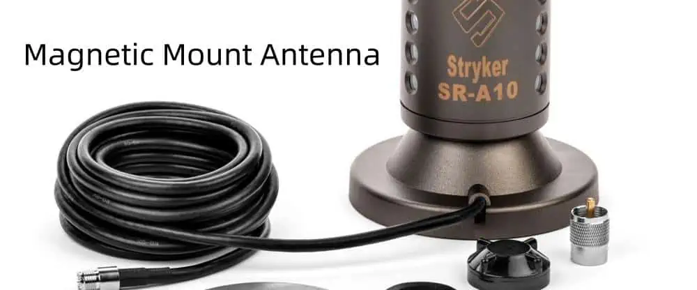
You can integrate a magnetic mount in an antenna base or use it as an accessory. Magnetic mount antennas are a great solution for positioning an antenna. They offer high signal strength and strong magnetic retention. The antenna stays firmly while on the move.

Magnetic mount antennas function well in road-ready radio, WiFi internet set-ups, and GPS. Reliable communication is of utmost importance in emergency, commercial, and industrial vehicles. Magnetic mount antenna is a must in these applications.ย  Magnetic mount antenna is a better solution than through hole antenna where you need to create a hole on a surface.

How to Install a Magnetic Mount Antenna

The process of installing magnetic mount antenna is quite easy. However, having a good knowledge about some tips can make the entire process quicker and easier. You need to know some important things before you even commence the installation process.

Pre-installation tips

These tips help to make the installation a seamless process and as well prevent any damage to your antenna.

The center of the roof is the most appropriate place to install the magnetic mount antenna.  This helps to gain a good signal and wide coverage. It is perfect to mount the antenna on your truck, ensure it is mounted in a vertical way. This may impact the performance.

  • Avoid sliding the mount once you have placed it in the right location. Otherwise, it will cause a scratch on the surface.
  • You can use magnetic mounts on Vinyl roofs. It prevents redaction in holding power. Also, it can lead to loss in electrical capacitance. In the long run, this will disrupt the antennaโ€™s operation at certain frequencies.
  • Ensure your antenna is not closely mounted to another antenna. You can stick to 12 inches apart, most preferably 6 inches away. If it is closer than that, this could result in interference.

Installation tips

Having known some pre-installation tips, you can go ahead to install the magnetic mount antenna.

  • Clean off dust and debris from both the bottom and surface of the mount. You should endeavor to repeat this process anytime you are installing a mount.
  • Position the mount on the already cleaned surface and carefully lower it. Just place the mount in a downwards position to make the antenna function as a handle.
  • Once you are through with the first two steps. Then you can now use your magnetic mount antenna.

The Base of Magnetic Mount Antenna

A magnetic mount antennaโ€™s base works with the magnetic principle to fix the antenna onto the surface of a metal securely. Because this attachment is not permanent, it serves as a great and flexible option for different applications. Most magnetic mount antennas are made up of radio frequency connectors that are enclosed in plastic casings. This keeps the magnets attaching to the antenna cables.

In addition, the magnetic mount antenna might feature rubber boots. This serves as added protection. Regarding cable length, size, magnetic strength, these magnetic mounts could vary.The heavy duty type of magnetic mounts feature three magnet bases. This type of mount is appropriate for any large antenna. Furthermore, you need to match each of them to antenna connectors or utilize ideal adapters.

During the installation of the magnetic mount antenna, there is a need to check out the strength of the antenna. This is so because magnetic attraction could cause the mount to snap and then cause injuries into you.

Why are Magnetic Mount Antennas used for Vehicles?

The magnetic mount antennas are usually utilized in vehicles. This is because it provides a quick as well as easy method of installing the antennas onto a vehicleโ€™s roof. Furthermore, these mounts provide better mounting options for custom rigs. Moreover, these mounts cannot work with soft top vehicle roofs.

The positioning of these mounts should be done in the location where the antenna will be screwed. The magnetic mounts will allow you to remove as well as adjust them wherever necessary. The removal of this antenna doesnโ€™t create any damage to the surface you mount it on.

Therefore, they can be easily deployed for emergency services and for use in the military. Radio enthusiasts can also use them as a mobile antenna. Dipole or monopole antennas integrate a magnetic mount. To achieve a firm hold, a monopole antennasโ€™ long rod conductor can be screwed using a magnetic mount. A good number of magnetic antennas incorporate the base-loading system with a special coil at the antennaโ€™s bottom.

Applications of Magnetic Mount Antenna bases

A wide range of applications make use of magnetic mount antenna bases. These antennas are especially useful where mobility is required. For instance, mobile antennas usually operate in motion. Magnetic mounts help in positioning vertically oriented antennas implemented in land-mobile operation to ensure there is undisrupted coverage. Below, we discussed some application where magnetic mount antenna base play critical functions.

GPS antennas

The profound radio navigation system in the world is the GPS. Also known as global positioning system, GPS is vital in wireless communication. Vehicles have GPS antennas and as such, must be exposed outside to make it GPS signal useful. Magnetic mounts can help GPS antennas on vehicles to stay in a firm position where there is enough exposure to the sky.

CB radio

Citizens Band radio (CB radio) utilizes magnetic mount antennas to ensure secure holds. CB radios are popularly used for making business and emergencies communications and as well as weather reports.

Emergency service vehicles

Antennas are critical for communication purposes. Mission-critical communications are needed in emergencies. Therefore, there is a great need for utility vehicles to have antennas that offer temporary solutions installed. One of the benefits of magnetic mount antennas is their ease of installment and removal. These antennas donโ€™t require you to use any special equipment when mounting them. This is what allows them to provide a reliable solution for some use cases such as utility vehicles or emergency service.

Storm chasing

This storm chasing takes record of harsh weather situations. People that storm chase require vehicle mounted instruments to help in meeting their meteorological and navigation demands. In most cases, some amateur GPS and radio frequencies can also track storms and then utilize radio for communicating with the other storm chasers. Magnetic mounts are useful for wind sensors or cellular antennas.

Related Questions

FULL PCB MANUFACTURING Quote

Is it possible to mount the magnetic mount antennas just anywhere?

If the magnetic mount antenna wonโ€™t be used on your vehicle, then locating the best magnetic surface for mounting this antenna could be difficult. All metal surfaces like cookie sheets or pizza pans could be appropriate for the installation of the magnetic mount antennas.

Can magnetism impact the performance of the magnetic mount antenna?

 No, this antennaโ€™s magnetic attraction cannot have an impact on how it operates or functions. This is so because magnetic field could have any effect on the receiving or transmitting signals. The magnetism only helps to firmly secure the mount to the metallic surface.

How do you place a magnetic mount antenna on the roof of a vehicle?

When mounting this antenna, ensure you prioritize height and centering. Centering this antenna on a convex roof increases its height.

Conclusion

Magnetic mount antennas are easy-to-install solutions for different applications. These antennas can grip a good surface due to their magnetic mounts. Magnetism is the basis of the functioning of these antennas. Since they are easy to position, they help you get good placement. Magnetic mounts donโ€™t leave any dent or scratch on the surface on which they are installed. You can easily remove this mount.

The Importance Of Choosing A Reliable Vape PCB Manufacturer: Ensuring Quality and Safety

Vape Pcb

In the past few years, Vaping has become one of the most popular alternatives to traditional smoking. PCB or circuit board plays an essential role in the production of vaping devices. With the rising demand for vaping devices, the demand for PCB is also increasing. The PCB in a vape considers a brain that controls several essential functions and ensures an efficient and safe vaping experience. This article gives you a detailed insight into the importance of choosing a reliable manufacturer for your Vape PCB. In addition to this, it explains the key factors to look into while choosing a Vape PCB CM, the benefit of using high-quality PCB, and how it affects the overall performance of vaping gears.

Vape PCB Role

Vape PCB refers to a core unit of an electronic vape. They consider one of the most complex components which manage power distribution, regulate the temperatures, control the IU function, and ensure the safe functionality of the vape. These essential and tiny circuit boards manage critical tasks, which makes them crucial elements in providing a seamless experience of vaping. It is vital to source Vape PCB from a highly reputable contract manufacturer as it ensures the performance, safety, and reliability of the vape. Moreover, make sure that a manufacturer must follow all industry standards, prioritize quality, and is best known for its reliable electrical device production.

The Significance Of Selecting A Reliable Vape Circuit Board Manufacturer

Vape PCBA Board
Vape PCBA Board

Selecting a highly reputable and reliable manufacturer of a vape PCB is of high significance as it ensures the safety and quality of the end product. However, the following are some key factors that ensure the significance of selecting a trustworthy Vape circuit manufacturer.

ยท       Ensure High-Quality

A trustworthy vape circuit manufacturer follows strict measures of quality control throughout the process of manufacturing. They use highly advanced equipment, technologies, and high industry-standard analysis to meet the required standards and specifications of a PCB. However, the quality of vape PCB leads to the development of a durable and reliable device for vaping in the end.

ยท       Follow All Safety Regulations

ย A vape device has to follow several safety regulations and standards to ensure the safety of a user. However, a reputable manufacturer comprehends these designs and regulations of a PCB that meets the necessary standards of safety. Therefore, a vape circuit manufacturer who follows all the safety protocols puts your heart at peace as you will get a high-quality PCB in the end.

ยท       Offers Customization

The different vape comes with unique specifications and features; therefore, they need a specific design of the PCB to accommodate those features. However, a reputable vape circuit manufacturer offers a unique customization choice that allows the device fabricator to mend the PCB according to their requirements. Moreover, this flexibility allows optimal functionality and seamless incorporation with other electrical components of a device.

Factors To Look at While Selecting A Vape Circuit Board Manufacturer

There are various factors to look into while selecting a Vape circuit manufacturer. All these factors play an important role in the end product. These factors include

ยท       Reputation And Experience

Check the experience and reputation of the manufacturer in the market. A highly experienced manufacturer provides a sense of expertise and reliability. In addition to these, a sense of understanding of the challenges involved in the production of high-quality vape PCB devices.

ยท       High Standard Of Quality

Make sure that the manufacturer follows strict standard of quality and certification like ISO 9001 as this certification depicts the quality commitment of the manufacturer and provides continuous quality experiences throughout the process of manufacturing.

ยท       Access To Advanced Technology

Ensure that the manufacturer must have all the advanced technologies and equipment for handling and producing complex designs of PCB. The high-tech, advanced equipment and efficient production process all contribute simultaneously to the performance and quality of a PCB.

ยท       Testing And Prototyping Capabilities

Check whether the manufacturer provides prototyping services along with strong testing analysis. Prototyping gives access to evaluate the design of PCB thoroughly before producing them in abundance. This allows the PCB to get the optimal performance of the PCB. On the other hand, strong testing analysis guarantees that every circuit meets the necessary specifications and performs well under several conditions. 

ยท       Follow Industry Standards

Check whether the manufacturer follows the standard of the industry, like IPC-A-610 and IPC-A-600, or not. Following these standards shows that this manufacturer follows ideal practices in the manufacturing, assembly, and testing of PCB. This, however, leads to reliable and high-quality products.

ยท       Management Of the Supply Chain

Check the management of the supply chain of the manufacturer as this ensures a reliable and steady supply of vape PCB. An efficient supply chain reduces the chances of disruption and delays. This gives a sense of the reliability of timely delivery.

ยท       Better Customer Support

Look for manufacturers that give importance to open communication services and customer support. Moreover, effective communication allows the manufacturer to understand your requirements and requests properly. This, however, also helps in times of issues and concerns.

ยท       Cost-effectiveness

Cost is one of the important factors to look for. Check whether the cost and quality a manufacturer is offering match or not. Moreover, lower prices may affect the quality, which eventually leads to performance problems and safety issues.

The Benefit of Reliable Vape PCBs

FULL PCB MANUFACTURING Quote

If you invest in highly reliable and quality vape circuits, you will get several benefits overall. However, some of these benefits contain the following:

ยท       Increased Performance

High-quality circuit boards ensure precise temperature control, efficient distribution of power, and an easy-to-use user interface. This, however, results in a prime vaping experience.

ยท       Improved Durability And Reliability

A reliable PCB reduces the chances of premature failures and malfunction. This, however, leads to reliable and longer-lasting vape devices.

ยท       Safety Assurance

Well, a well-designed circuit board with complete safety features minimizes the chances of unwanted accidents like short circuits or overheating. This, however, ensures the safety of users.

ยท       Positive Image Of Brand

High-quality and reliable PCB production makes the reputation of brands. In addition to this, they gain immense popularity and trust among customers for providing a safe and reliable experience of vape.

Conclusion

Choosing a trustworthy vape circuit board manufacturer is essential to ensure the performance, safety, and quality of the vape. A highly reputable manufacturer uses their expertise, follows the necessary standards of the industry, and gives a seamless IU for a safe vaping experience. However, you can easily select a trustworthy manufacturer if you look into some factors.

These factors include quality standards, compliance with rules and regulations, and customization. Looking into these factors ensures that manufacturers provide a high-quality, reliable vape PCB that follows all the industry standards and rules and meets all your requirements.

Therefore, investing in reliable vape PCBs not only proves beneficial for manufacturers in building brand reputation and trust around customers but also increases the overall functionality of the vape. Hence, it is very important to think carefully and wisely before selecting any vape circuit manufacturer.

How to Remove SMD Chip with Hot Air

Remove SMD Chip with Hot Air

These days, a wide range of electronic devices comprise SMD components, these include the SMD chip or ICs. Therefore, it is very important to know how to remove these SMD components from printed circuit boards or electronic devices. You will need to remove SMDs when there is a need for repair or replacement.

There are many ways you can remove an SMD chip. In some cases, a hot air station can carry out some solder jobs a soldering iron can’t. The hot air rework stations make use of hot air to desolder or solder an SMD component. Our discussion in this article will focus on how to remove an SMD chip with hot air.

How to Use Hot Air to remove an SMD Chip

It is always advisable to practice on an old circuit board if it is your first time removing SMD components with hot air. You can use a new board when you have already acquired the necessary knowledge and skills.

In some cases, you won’t know the solder has gotten to a molten state since there little solder is used for soldering the components.

Typically, the melting point of a lead-free solder is usually about 217ยฐC. Therefore, you need to ensure the pads and leads are up to the required temperature before you remove the SMD component. You will need a higher temperature since the solder joints needs to reach the melting point quickly.

In cases whereby the temperature of the hot air gun is lower, the solder joints won’t get to the melting point on quickly. The temperature of the component will increase if it takes a longer time to increase the pads or leads’ temperature. Therefore, it is much better to heat the component, remove it and the hot air gun. The part can be placed in a good environment to cool off.

One important thing PCB assemblers need to understand is to always treat their oxidized solder joints by using leaded solder. Do this before you begin with the hot air stage. Also, preheat the circuit board to 200 degrees Celsius after the process of mixing the solder. You can then continue to use the hot air station.

Why Hot Air is used for Soldering and Desoldering SMDs

Hot air is usually used during soldering and desoldering of SMDs. You can also use it for repair work. Even sometimes, you can use it to recycle the components of mobile phone and your PCs. Engineers easily use a hot air blower to remove electronic components from PCBs.ย  Also, metal parts can be desoldered without using a soldering iron.

When using hot air to desolder SMDs, heat up the soldering joint with hot air and warm up solder, after this, the components will carefully detach. Hot air can help you save some time as well as existing parts that you might consider trashing with the circuit board.

Sometimes, a hot-air rework station can act as a soldering station. This reveals a lot as you can desolder a resistor and solder another one. Hot-air is great for getting rid of SMD chips, especially multi-pin ICs. Over time, hot air has proved to be very efficient in desoldering PCB components. But, engineers and designers have to be completely sure they put certain things in place. For instance, the nozzleโ€™s size, air flow, and temperature of the hot air must be accurate.

Things to Watch out for When Removing SMD Chip with Hot Air

Detaching SMD chip by integrating hot air requires careful attention. This is because there are some errors that are likely to be made during this process. This is why you should ensure your tools are readily available. Below are some of the things you must consider:

The tools must be right for the job and must be available

To ensure the process goes smoothly, you need to work with the right tools. It involves a reliable soldering iron, soldering flux, desoldering braids, as well as heat gun. The whole process can be easy for you whenever you are working with the right tools. In addition, there is a low chance that any damage will happen to your SMD integrated circuit as well as the other components of the printed circuit board.

The temperature level

During heat exposure, SMD components become highly vulnerable and for extreme heat, the SMD chips could be completely destroyed. This is why it is advisable users take note of the temperature level they are making use of

Careful cleaning

Immediately you are done taking out the old solder, you have to clean the dirts found inside the chip. One tool that is very important here is the soldering flux.Proper cleaning will help the new component attach firmly to the board.

Testing

It is important to always carry out tests when you remove SMD chips with hot air. Errors could occur during this process and early detection could help to prevent further damage. Therefore ensure you test your components.

Possible Consequences of Using too High Temperature.

The application of hot air to remove SMD components usually require a level of temperature. If the temperature used is more than the required temperature level, some damages could occur. So, what are the possible consequences of setting a high temperature.

Component damage

When the temperature is set too high, it  can cause serious damage to the SMD chips including other components like  resistors and capacitors. This may result in failure or malfunction.

Toxic fumes

When the temperature is extremely high, the solder and flux can produce toxic fumes which is poisonous to humans and their environment. Therefore, we recommend engineers to work in an environment that is well-ventilated. Also, they should wear protective gear for safety purposes.

Too much solder flow

There could be too much flow of solder when the temperature is extremely high. This can lead to problems like cold joints and short circuits. These problems can make a circuit malfunction.

Advantages of Hot-Air Rework Station

Fast and Safe

Engineers who carry out repair work on electronic devices know the importance of hot air rework stations. Using hot air for your rework helps you to easily solder and remove any SMD components without mistakes. The hot air reworking method offers a high level of accuracy. Therefore, this makes it easy to easily remove any faulty electronic components form a circuit board. Also, you can easily install a new component in a twinkle of an eye.

Moreso, your hot-air gun’s nozzle shouldn’t come in contact with the boards. Therefore, these aspects reduce any possible damage to other parts of the board that could be caused by overheating.

Multiple functionalities

Since hot-air rework stations serve different functionalities, you can use them as primary soldering stations. This is a preferred way of removing SMD chips from electronic boards. There are other hot-air soldering station versions that offer more functions like screen printing for reattachment reflow. Also, these stations are accurate and very convenient to use.

What is the Ideal Temperature for Removing SMD Chips?

FULL PCB MANUFACTURING Quote

SMD chips are usually small in size. A good amount of heat is needed to detach these components from a board. This is the major reason you should make use of the required temperature.  If the temperature is okay, you will do away with the solder. But you need to know that, no particular amount of temperature is ideal since this all depends on some factors.

For instance, the melting point of a leaded solder is less when compared to a solder that is lead free. This is why you need to use a lower temperature when trying to remove any SMD component. Furthermore, when taking out the SMD chip with the hot air, place the temperature within the 350 to 380 degrees centigrade range.

How Can You Use the Hot Air Rework Station?

It is very important to handle hot air tools properly. This helps in preventing the falling of the tool. With the guidelines we have highlighted below, you should be able to utilize the hot air tool effectively.

  • To make sure thereโ€™s stability, hold this tool firmly. Make sure your skin doesnโ€™t touch its hot part
  • Make sure this tool is higher than the part to be soldered. Heat up this area using the circular motion
  • Place small quantity of solder on the end of each wire and then ensurefree flow over the track. The solder must look like the shape of a volcano.
  • Take away the hot air when the whole process has been completed.  Allow the board to cool before moving it.
  • Confirm the joint to see if it has a volcano shape. You can as well put more solder on it. Before adding more solder, ensure the lead and track have gone through proper heating.

Conclusion

SMD chips are vital components and it can be a daunting process to remove them from a PCB or electronic device. The best way to bring out these chips is to use hot air. Hot air can also get rid of other SMD components like transistors and resistors.

How to Control Bow and Twist in PCB ?

Bow and twist in PCB

Introduction

A printed circuit board (PCB) refers to the board made of laminated copper and insulating dielectric material on which electronic components are mounted and interconnected. PCBs form the core of all electronic devices and equipment. An ideal PCB should be perfectly flat without any deformation. However in reality, some amount of bow and twist distortion is often seen to occur in fabricated PCBs. Excessive bowing or twisting can create problems during PCB assembly as well as component reliability risks. Therefore it is critical for PCB manufacturers to have sound understanding of the root causes and implement optimal panel designs, material selection, layout strategies, and fabrication processes to minimize bow and twist.

This article provides a detailed overview of PCB bow and twist – how it occurs, the problems it creates, techniques to predict and control it during manufacturing as well methods to counteract bow and twist in circuit board assembly.

What is Meant By Bow and Twist in PCBs?

BOW Twist PCB
BOW Twist PCB

Bow refers to deviation of the PCB surface from perfect flatness resulting in either convex or concave shape. It occurs due to stresses in the board leading to outward bending. Bow is quantified as the measurement of maximum deviation from a reference plane along the length/width of the board.

Twist indicates the amount of distortion in the planar form of the PCB causing the corners to rise above or sink below the center plane. The four corners of the board are no longer coplanar due to rotational forces on the board. Twist is characterized by the maximum out-of-plane deflection between two diagonally opposite corners.

Here is an illustration depicting bowing and twisting of a PCB:

Bow and twist deformations are largely unavoidable in PCB fabrication. The aim should be to control these within acceptable limits rather than try to eliminate them fully.

Causes of Bow and Twist in PCBs

Some key factors that create stresses leading to bowing and twisting of PCBs are:

Differences in Coefficient of Thermal Expansion (CTE)

During the lamination process, the conductive copper layer, dielectric substrates and prepregs are bonded together under heat and pressure. The different expansion coefficients mean that during cooling after lamination these materials shrink by varying amounts. This creates stresses in the board leading to deformation.

Composite PCB Construction

The laminated stackup of heterogeneous materials – conductive layers, dielectric substrates, vias etc. each react distinctly to temperature and moisture. Absorption or desorption of moisture also alters dimensions differently. These combine to induce bow and twist forms.

Panel Automation Effects

PCBs are fabricated in large panels which undergo thermal and mechanical stresses during processing through conveyor ovens, copper plating tanks etc. Non-uniform stresses on the panels can result in shape distortions.

Internal Layer Misregistration

Any mismatch between position of internal layers and outer layers during lamination registration will inherently induce stresses and deformation. This effect grows with number of layers.

Plating Stresses

Significant localized stresses are generated during electrolytic copper plating which can reach over 0.5 pounds per square inch. This tends to create panel bowing and twist deformation.

Thermal Metal Deposition

During sputtering or vapor deposition of metals for surface finishing, high directional stresses occur which bend the thin panels.

Uneven Support and Tooling

During PCB panel movement between processes, uneven tooling contact or inadequate support can create flexing and distortion in panels.

Routing and scoring

Stresses induced by mechanical routing and scoring of panels to create individual PCBs from panels introduce twist and bow if not controlled.

The combination and interaction of multiple such factors during fabrication makes bow and twist very difficult to avoid completely in PCBs. Careful analysis and planning is needed to minimize them.

Problems Caused by Excessive Bow and Twist

Significant bowing or twisting shape distortion in PCBs creates several problems during manufacturing, assembly and functioning of the board which highlight the need for bow/twist control:

Reduces Assembly Yield

Excessive bow or twist will prevent proper seating of component leads in plated through holes. It hampers placement of smaller surface mount components. This directly increases assembly defects and reduces manufacturing yield.

Affects Coplanarity

Non-coplanar PCBs due to distortion interfere with mounting of quad flat packs, ball grid arrays and other devices needing flat contact pads. Solder joint stresses also increase.

Hampers Reliability

Stresses induced in solder joints and plated through holes due to board distortion negatively affect reliability of solder/PCB interconnections.

Increases Rejection Rate

Higher levels of bow and twist will fall outside permitted tolerance limits leading to rejection of fabricated PCBs. This increases cost.

Limits Panel Utilization

To counteract bowing, panel sizes may need reduction. Smaller panels mean lower PCBs per panel leading to higher cost.

Interferes Electrical Testing

Twisted boards cannot make flush contact with test fixture pins. Gaps create false failures and unreliable test results. Fixture damage can also occur.

Creates Rework Issues

Bowing and twisting results in PCBs failing during assembly process tests. This interrupts production flow and necessitates expensive rework.

Restricts Component Choices

Larger or heavier components exert greater stresses worsening deformation. Component size and weight limits may be needed.

Increases Costs

Overall PCB cost increases due to lower fabrication yields, more rework, panel size restrictions, component limitations etc.

Quantifying Bow and Twist in PCB Standards

How to Prevent PCB Bow and Twist

To ensure quality and interoperability, PCB standards like IPC-A-600 provide acceptance criteria for maximum permissible bow and twist. testing methods to measure bow and twist are also defined.

Bow Measurement

As per IPC-TM-650 method 2.4.22.1, a taut wire or string is stretched across two edges of the diagonal of the PCB panel. Using a dial indicator, the maximum deviation from the reference wire is measured. This quantifies the board bow magnitude.

Twist Measurement

To measure twist as per IPC-TM-650 method 2.4.22C, two opposite corner pins stretched by rubber bands touch the PCB corners. The height difference between the other two corners indicates the degree of twist.

IPC Standards for Bow and Twist

The IPC-A-600 Acceptability of Printed Circuit Boards covers maximum permissible bow and twist in PCBs:

PCB ThicknessBowTwist
โ‰ค 1.6 mm0.75%1.5%
1.6 to 3.2 mm0.75%1.0%
โ‰ฅ 3.2 mm0.5%0.75%

Note:

  • % is based on the diagonal distance across the PCB
  • Both bow and twist total should not exceed 2%
  • For stiffeners and metal core boards stricter requirements apply

Techniques to Predict Bow and Twist

During the design phase itself, analysis methods help predict the bow and twist expected based on the PCB materials and layer stackup:

CLPT Analysis

Curved Beam Macromodel uses laminated plate theory to calculate thermal stress based on CTE mismatch and simulate distortion.

FEA Tools

Finite element analysis tools like Ansys, Comsol etc. can construct 3D PCB models and compute deformation under simulated process stresses.

Analytical Calculations

Manual calculations using plate theory provide approximate bow/twist values for simple geometries based on metal/dielectric thicknesses, dimensions and CTE values.

Process Modeling

Mass curing models mimic the actual curing conditions like temperature ramps, vacuum pressure etc. to forecast panel warpage.

Historical Data

Statistical regression modeling based on correlation between previously observed bow/twist values and PCB design attributes.

By predicting potential bowing and twisting early, the PCB can be optimized during design before fabrication.

Guidelines to Minimize Bow and Twist

While some bowing and twisting is unavoidable, following design and fabrication guidelines help reduce it:

Symmetric Layer Stackup

Balancing metal/dielectric layers equally about the centerline minimizes deformation due to thermal stress imbalance.

Balanced Copper Distribution

Equalizing copper densities on either side of the PCB centerline maintains symmetry and avoids bow-twist from uneven contraction.

Thinner Dielectrics

Using prepregs and bonding sheets under 100 ฮผm thick lowers thermal stress mismatch between metal and dielectric.

Tailored CTE Dielectrics

Prepregs with CTE values between the extremes of copper and FR-4 (17 – 21 ppm/ยฐC) produce less thermal stress and warp.

Low CTE Reinforcements

Embedding glass fabrics with very low CTE (2-5 ppm/ยฐC) in prepregs counteracts excessive composite thermal expansion.

Low Stress Plating

Reducing plating bath stresses and operating at lower current densities lessens panel warpage from plating.

Balanced Panel Cutout

Symmetrically placed panel cutouts balance internal stresses and prevent excessive distortion.

Perimeter Support Tooling

Contact tooling around the panel edges minimizes unsupported bowing during lamination and plating processes.

Bow Reducing Routers

Routers with rigid linear motors, granite beds and linear encoders precisely score panels reducing induced stresses.

Methods of Correcting Bow and Twist

Bow and twist in PCB

In addition to built-in panel design and process steps aimed at minimizing bow/twist, some corrective techniques are also deployed:

Panel Symmetrization

Selectively removing copper from one side and adding dielectric layers counteracts asymmetric construction causing deformation.

Stress Relieving Anneal

Post-etch bake of panels at over 180ยฐC relieves some internal stresses induced during fabrication thereby reducing warpage.

Bow-Twist Correction Fixtures

Applying localized heat and vacuum pressure in chambers with precisely positioned industrial vacuum cups counters panel distortion.

Corner Support During Handling

Dedicated tooling with adjustable corner pins for supporting panels during handling avoids inducing bows and twists.

Panel Splicing

Cutting a large panel into smaller pieces can lower internal stresses and achieve flatter individual PCBs. But utilization suffers.

Flattening Pressing

Applying high uniform pressure between flat plates compresses top and bottom panel surfaces towards a common plane.

Mitigating Bow and Twist Effects During Assembly

While fabricating optimally flat PCB panels is ideal, somebow and twist is unavoidable. Steps can be taken during PCB population and final product assembly to mitigate issues:

Robust Component Securing

Using adhesive along with fasteners or connectors to securely fasten components like heatsinks prevents them from worsening PCB shape.

Board Stiffening

Strategically bonding stiffeners like metal strips or plastic grids on panel backsides supports flatness.

Stress Relieving Anneal

Heating fully loaded boards to over 100ยฐC then cooling slowly in controlled fashion can relieve built-in deformations.

Selective Conformal Coating

Applying conformal coating over stressed board sections provides reinforcement against twisting or bending further.

Blanket Foam Layer

Placing foam sheet layer across backside dampens and absorbs mechanical stresses preventing distortion.

Clamping During Soldering

Using fixtures or weighted tops during reflow soldering minimizes movement and reinforces board flatness.

Panelized Assembly

Retaining PCBs in panelized format through assembly avoids introducing stresses from de-panelization.

FAQs

How are very thin and flexible PCBs tested for bow and twist?

Thin boards are tested sandwiched between metal plates to temporarily reinforce them during measurement.

Does solder masking process influence bow and twist?

Yes, poor mask adhesion or excessive mask thickness imbalance on panel surfaces can initiate or worsen bow/twist deformation.

Can soldering process induce or aggravate board warpage?

Yes, if components only loaded on one side, soldering can create asymmetric thermal stresses bowing the panel.

Is moisture absorption a factor in PCB bow and twist?

Yes, moisture absorbed by the dielectric substrate laminations causes greater expansion than copper, resulting in bowing and twisting stresses.

How to reduce bow and twist in multilayer HDI PCBs?

Use thin prepregs, symmetric spread of layers across centerline, dummy metal fills to balance densities, and selective stiffeners on panel.

What are the Main Features and Benefits of the FPC Antenna?

FPC Antenna

Flexible printed circuit boards usually work with the wireless antenna designs. It does this effectively, so as to supersede the antenna with respect to the traditional PCB, and then offer free dimension of the integration of the wireless system and antenna to the designer.

What are the Materials Used for the FPC Antenna?

Since the FPC antennaโ€™s adhesives are usually affixed to other substances, the adhesiveโ€™s secondary adhesiveness would experience a reduction. Also, if the copper cloth corners are bent, you can attach them to the shellโ€™s surface with a less curved radius.

Furthermore, due to stress from bending, it can easily experience warping. This is why when separating the FPC antenna from the adhesive paper, donโ€™t bend at the two ends of your antenna. In addition, you should not touch the adhesives present on the two antenna ends using your fingers. This is because these ends are known to receive the highest bending stress. Ensure that the adhesives on both ends are kept clean and prevent creases on copper cloth regions at both ends.

Usually, FPC antennas are thin, and are just 0.15 mm. Also, they feature a strip that is peelable, as well as an adhesive section. All these can be fitted into smaller electronic devices and in different configurations. Also, they are usually supplied with a connector and a cable. These are used for fixing them into the bottom housing or cover of the electronic product of the manufacturer. FPC antennas are usually lightweight, below 1 gram.

What are the Features of the Flexible PCB Antennas?

FPC board Antenna
FPC board Antenna

The FPC Antennas are low profile, flexible, and very economical and reliable antennas, which are widely utilized in wireless industries. This antenna is made of polyimide flex PCB that has a patterned and conductive material (usually copper) for the best antenna topology.

You can use it in developing different antenna types. These include dipoles, monopoles, as well as the printed F antenna. These antennas have coaxial cables which help in connecting to the needed circuit.

Main features of the FPC Antenna

You can bend the FPC antennas to ensure their embedding into small devices like the IoT module whereby the space in the circuit board is at premium and you cannot place the surface mount antennas.

Furthermore, you can place the FPC antennas horizontally, vertically, and co-planar to the parent PCB without affecting the performance. These antennas perform in a consistent manner when on curves, when flat, or when vent to some degree. This is why they are appropriate for devices whereby the SMD antenna wonโ€™t fit into the parent PCB with the needed ground place.

Also, you can customize the FPC antennaโ€™s cable length, which makes connection to modules very easy. Traditionally, a PCBโ€™s size and its accessible ground planes usually affect the SMD antennaโ€™s performance. However, this isnโ€™t applicable to the FPC antenna, because the flexible circuits has been customized for that antenna placed on it. What this ensures is higher performance levels, space saving, as well as fewer steps in integration.

The flexible printed circuit provides a similar performance whenever it is compared to the external omni directional antennas such as omni directional radiation patterns as well as high efficiency levels. However, it needs less ground space to be able to achieve these performance levels. Therefore, these antennas usually optimize the circuit board for them to function.

With respect to cost, the FPC antennas are less expensive than the externally mounted types. You can achieve high performance levels without having to deploy external antennas. You can fabricate the FPC antenna making use of standard techniques of PCB manufacturing. This makes them repeatable antennas and very reliable. 

The Advantages of FPC Antenna has no Ground

SMD chip antenna and the FPC antenna have different working principles. SMD antennas utilize the ground plane (already installed) for radiating and its principle for working is reciprocating. Also, dipole antennas make use of two radiators, and each radiatorโ€™s length is associated to the frequencyโ€™s wavelength that is utilized by that antenna. Also, embedded antennas feature heat sinks within its mass range, and they utilize areas on the printed circuit board as its counterpoint, which is also its ground plane.

For the SMD antennas, the ground planeโ€™s length is related to the antennaโ€™s wavelength. You have to provide the right ground plane into the design to ensure the antenna will be able to operate with great efficiency.

At this stage, FPC antennas act differently because they donโ€™t require ground planes to offer radiation. This is why they allow designers to arrange the circuitโ€™s components freely into the design.

However, this coaxial cable now forms part of an antenna. During the design of the cable extender of the antenna, you should take care to ensure that this component of the antenna is taken away from the remaining components which might create interference and noise.

Placing Your FPC Antennas

Because ground planes arenโ€™t a consideration for FPC antenna design, the parent PCB size isnโ€™t a factor such as chip or SMD antennas. Moreover, placing FPC antennas must follow some important rules, since the majority of antennas are usually sensitive to their environment.

This antenna radiates in six different spatial directions. These are right, left, back, front, down, and up. Ideally, in 3 to 5 of the directions, you shouldnโ€™t have any obstacles. This allows the antenna to function effectively. Also, for the other directions having obstacles on its radiation oath, a minimum gap still has to exist, which would be specified in the antenna datasheet of the manufacturer.

Furthermore, the deviceโ€™s plastic casing wonโ€™t behave as an obstacle. This can only happen if the casingโ€™s material is painted in a metallic way or is glass filled. The metal components and objects near the FPC antenna like PCBs and data lines are usually the culprits blocking the signal.

Requirements of the FPC Antenna Direction

FULL PCB MANUFACTURING Quote

The deviceโ€™s shape determines the appropriate orientation of a FPC antenna in relation to the circuit board. The antennaโ€™s position relative to the circuit board would depend on the ground wireโ€™s proximity.

No matter the chosen solution, the distance is now an important design dimension. This would be indicated in the datasheet of the manufacturer.

In addition, the antennaโ€™s I-PEX connector cables connect it into the design. Also, the design of this characteristic impedance of the transmission line inside the product should be 50 ohms and has to be kept very short. All the other components of a radiofrequency system like power amplifiers and transceivers must be designed to have a 50 ohm impedance value.

To build the layout of your transmission line, we advise that you utilize a commercial radio frequency design package. You must take into account the dielectric constant, copper thickness, and PCB thickness. This program would calculate the transmission lineโ€™s required width as well as the proper spacing between an antenna feeder and the ground planes on the two sides to be able to maintain a system impedance of 50 ohms.

FPC Antenna vs PCB Antenna: Whatโ€™s the Difference?

Traditionally, a PCBโ€™s size along the ground plane will have a direct influence on the SMD antennaโ€™s performance. This isnโ€™t applicable to the FPC antennas, as flexible circuit boards are customized for whatever antennas are placed on them. This permits high performance levels, space saving, as well as lesser integration steps.

The FPC antennas provide similar performance whenever it is compared to the external omni directional antennas such as omnidirectional radiation patterns, as well as high efficiency levels. However, it needs a smaller ground space in order to achieve these performance levels. Therefore,. These antennas help in optimizing the circuit boards to deliver their functions.

In addition, FPC antennas are less expensive than the PCB antennas (the externally mounted ones). You can achieve high performance levels without having to deploy external antennas. You can fabricate the FPC antenna making use of standard techniques of PCB manufacturing.

This makes them repeatable antennas and very reliable. Also, the FPC antennaโ€™s adhesive backing ensures the easy mounting of the FPC antenna family in custom and unique enclosures, coupled with enabling an enclosure that is environmentally sealed and protection from accidental damage to the antenna or tampering.

Furthermore, FPC antennas perform well in different applications. These include cellular IoT, wideband cellular sub-6 5G, 4G, 3G, and 2G, 5G New Radio, etc.

Will FPC Antenna Suit Your Design Appropriately?

For the small printed circuit boards, the SMD antennas might be the obvious choice. However, FPC antennas are very useful in applications having insufficient space.

The off-the-shelf flexible printed circuit antennas arenโ€™t recommended for smallest devices. However, many applications exist whereby FPC antennas function effectively. They are very useful alternatives for the designs whereby the ground planeโ€™s space and length are limited.

Conclusion

In summary, the FPC Antennas are low profile, flexible, and very economical and reliable antennas, which are widely utilized in wireless industries. You can bend the FPC antennas to ensure their embedding into small devices like the IoT module. Furthermore, you can place the FPC antennas horizontally, vertically, and co-planar to the parent PCB without affecting the performance.

DFM Tools: Picking Proper DFL (Design for Manufacture) Tools for your Design

PCB DFM

Before your product gets past the process of design and into the manufacturing process, the DFM standards have to be met. This is why the DFM tools are very important to ensure that the design of the product works in line with DFM requirements.

This also holds for PCB fabrication, whereby the design of the board must work in line with the design rules in order to reduce manufacturing failures. In this topic, we will be analyzing the DFM tools as well as their principles. Let’s begin.

What Does DFM Mean?

Design for manufacturability can be described as an engineering practice utilized for designing products in such a unique way that makes their production easy and at the lowest price possible. Also, with DFM, you will be able to fix possible errors like alignment issues during the design stage. This is because it is at this stage that you can address these issues at a lower cost.

If this isn’t done, the product could have both reliability and performance problems all through its life cycle. Also, note that every process in manufacturing comes with its design rules. Explaining further, a process of additive manufacturing – 3D printing, features different guidelines for design compared to CNC machines, which is just a subtractive process of manufacturing.

Therefore following the design guidelines for individual manufacturing processes when designing the components of products is important. Also, with PCBs, you can monitor the thickness of the board, minimum diameter of the via hole, surface finish, as well as the minimum trace width. Asides from reducing possible errors and unit price, DFm can help reduce the turnaround time.

What are the Principles of DFM?

DFM Tools
DFM Tools

Design for manufacturability is composed of five main principles.

Process

The process of manufacturing you have chosen must be suitable for the product. Also, during the consideration of the process, the DFM has to consider some factors, which includes required tolerance, surface complexity, etc.

Design

This DFM principle is most critical. This is because it allows users to customize a product, thereby giving it a layout that is optimized which reduces costs of manufacturing, faults, as well as turnaround time. Reach out to your manufacturer regarding the design of the product. This ensures that it works with the most appropriate processes of manufacturing.

Material

With DFM, you are required to choose the material with respect to properties such as thermal resistance, color, flammability, mechanical strength, electrical conductivity, etc. You should also take note of the cost of the material.

Environment

This product has to withstand the intended function and operating environment without issues.

Compliance/Testing

Finally, this product has to meet the necessary safety and quality standards that could be industry-specific, internal company, as well as third party standards.

What Do DFM Tools Mean?

While the rules for PCB clearance were defined easily in past times, the present DFM rules are dependent on different factors like hole diameter/spacing, trace width, etc. All these factors would help in creating many design rule checks which the PCB design software has to monitor

Therefore you have to set up these applications for CAD design to check the rules. This makes them the first DFM tools needed in the process of PCB production. Besides this PCB design software, different DFM tools present in the marketplace can tell which layers of the board have production issues. Most times, these tools feature a checklist that ensures a comprehensive analysis of the design layout of the PCB.

Also, DFM tools help in handling multiple checks so as to enhance the design manufacturability. Since you may not know whatever the processes your fabricator has used in making the PCB, it is advisable that the manufacturer handles the DFM check and then give you a report for your DFM.

Use Valor to Achieve Error-free Designs

Valor, which is well-known by MNCs, offers a great solution for PCB manufacturing.PCB forms the heart of all embedded systems and electronics hardware. Valor is an easy and seamless all in one tool. This tool helps reduce errors, ensuring that teams involved in the design as well as manufacturing don’t waste cost, labor, and time in detecting faults and rectifying them.

Once completed, the design will be checked utilizing Valor or other similar tools. Furthermore, companies such as Cisco have ensured the compulsory use of this tool because of its ability to produce complex PCBs up to 24 layers.

Valor features a checklist. These include checking of boards on PCB assembly, by each layer, which includes  pattern check and signal checks on-component basi, Gerber files, component counts, PCB impedance, copper pads, copper layers, through-hole pads and drill check.

Asides from these, a PCB’s quality check can be checked with respect to the application, and routing, thickness, punching, stencil paste, and stencil check is also considered. After this test, Valor will then differentiate between cold and hot points. These hot points will first be rectified, then tye cold points follow.

Also, Valor can handle calculations. A screen printing machine manufacturer should know the precise amount of solder paste applied on these stencils. Normally, the rate of transmission has to be at least 70%. Depending on the project’s size, it takes Value between 24 – 48 hours for calculation. Similarly, for other processes, there are some calculations required.

Users of Valor have to convert ERP or SAP, PCAD or CAD files, as well as other circuit board designs files and simulation files into the ODB++ format that is readable for valor.

Other Important DFM Tools

Apriori

A tool, referred to as Apriori, offers a unique platform that allows manufacturers to be able to manage the cost of their products all through the development and manufacturing stages.

This begins from the stage of design and then to the manufacturing stage. This DFM tool is focused on the way the cost of the project would be feasible and allow quick iterations with respect to the changing market, availability, and cost.

Project Tracker

Thereโ€™s another tool, project tracker that updates the tracking of different activities, events, assignments linked to the project. This assists the managers of the project in consistent execution of the project, improved utilization of resources, reduction in resource gaps, as well as operational frequency.

Also, it helps to facilitate decision-making and communication, allowing you to manage your project efficiently as well as deliver quickly. This makes the entire process budget-friendly and hassle-free.

Newly-created DFM tools like Cost-Out Analysis, Fast Works, as well as Should Cost Analysis works well for purchase and sourcing and are utilized by some top electronics conglomerates in America.

Monitoring the Cost During the Design Stage with Fast Works

FULL PCB MANUFACTURING Quote

Fast Works

An industry professional revealed that Fast Works functions well for developing new products inside a particular company. This allows you to get close to a customer, increase the chances of succeeding, and hasten the marketing as well as getting things done easily.

Most times, companies make use of Fast Work to cost during the development of new products, and then the launching of prototypes in a market place follows. This methodology has a stage whereby the team work is defined. This focuses on the weak points of the customer, thereby giving solutions as well as documenting the entire process.

Cost Saviors While Running a Product

Should Cost Analysis

This sets a proper benchmark for any cost negotiation. With this tool, designers will be able to get some clarity of the vendorโ€™s pricing. This ensures that informed decisions are made with respect to the componentsโ€™ cost.

This assists designers in reducing costs during the stage of design. SAP and Apriori are two significant tools used for the Should Cost Analysis. This analysis covers serviceability, price, customer satisfaction, quality, and technology.

For any product, companies utilize either Cost-Out Analysis or Should Cost Analysis. After this analysis, a designer might advise the customer to embark on a different project or give ideas for added features to the product. With this, you can manage design for manufacturing from its initial stage to the final stage

You might feel these tools are very important for a DFMโ€™s success; however, this isnโ€™t the case. Industry experts have revealed that tools such as Apriori, Valor, Project Tracker, and SAP are very important, some of them could be demanding and need rigorous training and a huge investment. Not every small-scale startup or manufacturing unit can purchase these. However, 3rd-party testing should always be an alternative.

An alternative here is a DFM rulebook which could be manufactured by experienced manufacturers and designers, which design engineers can use.

Conclusion

In summary, the DFM really touches on the part of the customer (because of product designs) as well as the part of the manufacturer (because of the manufacturing process). This is why the manufacturing and design teams must communicate constantly so as to refine the DFM guidelines. All you need to do is visit our contact page and then drop your details, which includes your Gerber files. We will contact you as soon as possible to discuss possible DFM problems that may arise.

What is the Difference Between a Sector Antenna and an Omni Antenna?

Sector Antenna

Sector antenna can be described as directional microwave antennas having a radiation pattern with a sector shape. This word โ€˜sectorโ€™ is utilized geometrically. Some fraction of a circleโ€™s circumference measured in arc degrees.

120 degrees, 90 degrees, and 60 degrees, are typical, usually with few degrees more to make sure overlap occurs and also mounted in form of multiples whenever there is a need for a full-circle or wider coverage. The most important utilization of the sector antenna is for cell phone sites. Also, they are utilized for the limited range distances falling between 4 and 5 km.

In this article, we will explain everything elated to sector antennas. We will also state the differences between the sector antenna and omni antenna.

What Does a Sector Antenna Mean?

Sector antennas can be called sector panels, and they are directional antennas that serve outdoor applications. Most times, they are utilized by base stations, and they could be seen, as well as hung on the towers of cell phones. Also, they are narrow, long antennas that have high gains.

Furthermore, the sector antennas are made of different dipoles that are place in-front of shaped reflectors. Also, the reflectorโ€™s shape and size helps in determining their antennasโ€™ performance. Usually, this reflector is flat, and it comes with ridges along with other features present along its edges.

Most times, t5he sector antenna is categorized by its 3-dB azimuth plane width. Also, they are available in the 120 degree, 90 degree, and 60 degree directionality. These sectors are applied higher up inside air and its deployment height selects the necessary antenna because thus affects the antennaโ€™s range and gain.

More on Sector Antenna

The sector antennaโ€™s main reflection screen is made of Aluminum and this antenna features a radomes. This radome is made from fiberglass material and this ensures that the components remain in the antenna safe. It also ensures the antenna can withstand any harsh weather condition. The sector antenna is used for cellular communication extensively. The greatest use of the antenna is for the base station sites of cell phones.

The sector antennaโ€™s coverage area can be determined by the radiation pattern projection on the ground area. This could be adjusted by altering the antennaโ€™s down-tilt angle. There are models whereby this is mechanically done by adjusting the antennaโ€™s tilt manually with the adjustable mounting bracket.

 For sector antennas that are more recent, it is possible to tilt the pattern electronically. This is done through the phase shifters present inside the feed of the antennaโ€™s dipole antennas. You can adjust this with remote control circuits from the ground, getting rid of the need to get a technical to get to the antenna tower. In order to get coverage in 360 degrees, you should use multiple sector antennas and you have to mount them back to back.

The Design of the Sector Antenna

At the sector antennaโ€™s bottom region, you will find RF connectors. These are meant for the coaxial cable as well as adjustment mechanisms. Also, for the outdoor placement, its primary reflector is manufactured from aluminum, and all of its internal parts are all housed in fiberglass radomes enclosures. This is to ensure that its operation remains stable no matter the weather condition.

For outdoor antennas, grounding is very necessary. This is to ensure that all the metal components are DC grounded. The narrow long form of the antenna provides it with fan shaped radiation pattern. When in horizontal direction, it is wide, and when it is vertical, it is relatively narrow.

More on Sector Antenna Design

According to your depicted radiation pattern, typical antennas utilized in the three sector base stations feature 66 degrees of the horizontal bandwidth. What this means is that the strength of the signal present at the ยฑ33 degree directions is 3 dB down or half its usually peak value when at the middle or center.

Also, when it is at the ยฑ60 degree directions, then we suggest that it is a border of the sector and the gain of the antenna is negligible. The vertical bandwidth isnโ€™t wider than 15 degrees. This means 7.5 degrees in every direction. In contrast to the antennas that serve commercial broadcasting โ€“ television, FM, and AM for example โ€“ that has to achieve line of sight over many kilometer s or miles, thereโ€™s always a downward downtilt or beam tilt top ensure the base station will be able to cover the immediate area effectively and not lead to any RF interference to the distant cells.

 This coverage area that is determined by the radiation patternโ€™s projection onto the ground could be adjusted by altering the patternโ€™s downtilt. For some models, this could be mechanically done through adjusting the antennaโ€™s tlt manually with the help of the adjustable mounting brackets.

For sector antennas that are more recent, it is possible to tilt the pattern electronically. This is done through the phase shifters present inside the feed of the antennaโ€™s dipole antennas. You can adjust this with remote control circuits from the ground, getting rid of the need to get a technical to get to the antenna tower.

How to Use the Sector Antenna

In order to widen as well as increase the area for coverage, and your served clients, different sector antennas can be installed on one supporting structure, for example, a mast or tower.

This type of construction is usually referred to as the sectorized antenna. Although, there are times whereby sector antennas are utilized also. This features different secular antennas that are angularly separated.

Immediately the antenna has been attached to the supporting structure, it must be positioned. When we say positioning, we mean not just setting the correct azimuth or direction, but setting the right downtilt too. When you restrict emitted energy into narrow vertical coverage and sub-circular arcs, this design will make proper utilization of transmitter equipment with very low power.

Although there is a limited absolute range, the configuration permits great data rates (the transfer of digital information, calculated in bits per second, which is at times given as the full minus error-correction overheads), as well as great signal consistency in the coverage area.

More Tips on Using the Sector Antenna

Before positioning, lighting and grounding protection are very necessary. All the supporting constructions usually include lightning rods. Downtilt setting strategies that are properly chosen could reduce the networkโ€™ overall interference. Furthermore, a downtiliting strategy that is too aggressive would result in general coverage loss because the cells are not overlapping.

You can use downtiliting for solving some issues. These include too large cells, or local interference issues. The beam width is slightly reduced by electrical tilting.

Take note that more vertical antennas would be less visible compared to mechanically tiled ones. The utilization of just electrical tilt excluding the mechanical tilt would therefore be a great choice for different aesthetic reasons that are very significant for operators that seek the acceptance of the integrated antennas present in the visible locations.

Sector Antennas vs Omni Antennas: Whatโ€™s the Difference?

FULL PCB MANUFACTURING Quote

In this section, we will be comparing the sector antennas with the omni antenna. We will also be explaining the differences between both antenna types.

Often, people are inquisitive about the differences between the sector antennas and the omnidirectional or omni antennas. Both antennas look very similar, bit their functions are quite different. Below is a complete breakdown of the way they function. This allows you to determine the best option for your application.

From the name, the omni-directional antennas help in transmitting and receiving uniform signals through a pattern of 360 degrees. The omni antennaโ€™s radiation pattern looks like a donut having reduced coverage which is immediately above and below the antenna, as well as expanded coverage while you move away further from this antenna.

Because omni antennas have the ability to transmit as well as receive signals in all direction, they are usually utilized by WISPS having access points. These Omnis are appropriate for utilization in the rural environments whereby the initial subscriber counts could be low.

Sector antennas are grouped as the directional microwave type of antennas. In contrast to Omnis, the sector antennas would only transmit as well as receive the concentrated signals in just one direction. Also, the WISPs usually utilize the sector antennas to serve point to multipoint base station applications. Also, they are better suited to serve dense environments whereby there are higher subscriber counts.

Conclusion

In summary, sector antennas can be called sector panels, and they are directional antennas that serve outdoor applications. Most times, they are utilized by base stations, and hung on the towers of cell phones.

Also, they are narrow, long antennas that have high gains. In order to widen as well as increase the area for coverage, different sector antennas can be installed on one supporting structure, for example, a mast or tower. This type of construction is usually referred to as the sectorized antenna. Comparing the sector antenna and omni antennas, both antennas look very similar, but their functions are quite different

Types and Applications of Thermistor Circuit

Thermister Circuit

Thermistors are very important in a circuit, and no one can deny their importance in various circuits. They act like passive components in an electric circuit. Thermistors are cheap, durable, and easy to use in the system. You can find their use in everyday items such as digital thermometers and household appliances etc.

What is a Thermistor?

A Thermistor is a semiconductor type of resistor. The electrical resistance is dependant on temperature. The word ‘Thermistor’ is a combination of thermal and resistance.  Thermistors are super sensitive to temperature. That’s why their resistance varies with a slight change in temperature. When there is a change in the temperature, there will be a measurable change in the resistance of the thermistor.

They are composed of metallic oxide, which is molded into beads, disks, or cylindrical shapes. The epoxy or glass encloses them and further gives them waterproof properties. They do not work well in extremely hot or cold temperatures. They are precise when they are for a limited temperature range of about 50 degrees around the target temperature. The base resistance will show the range of the resistance.

Working Procedure of Thermistor in a Circuit.

Thermister Circuit Board

A thermistor works in such a way that its resistance is reliant on its temperature. If we know the relationship between how the temperature change will affect its resistance, then by measuring the resistance, we can derive its temperature. At the same time, the resistance changes depending on the material used in thermistors. The relationship between the resistance of a thermistor and its temperature is non-linear. You can use an ohmmeter to find out the resistance of the circuit.

Types of Thermistors

Depending on the working procedure, there are two types of thermistors.

  • Negative Temperature Coefficient (NTC) Thermistor
  • Positive Temperature Coefficient (PTC) thermistor

Negative Temperature Coefficient (NTC) Thermistor

NTC thermistors have the abundant uses in our life. The resistance of the NTC thermistor is inversely proportional to its temperature. NTC’s resistance decreases with the increase in temperature; usually, due to an increase in induction, the electrons are bumped up by thermal agitation from the valence band and vice versa. You can find them in temperature sensors or as inrush current limiters.

Positive Temperature Coefficient (PTC) Thermistor

PTC (positive temperature coefficient) thermistor is not as common as NTC. However, engineers use it as a fuse for the protection of circuits. PTC acts as a current limiting device.

When the temperature increases, its resistance also increases, usually due to increased thermal lattice agitations of impurities and imperfections. While the resistance of PTC decreases with the decrease in temperature.

Advantages of Thermistor

Thermistors have the following advantages:

  • They are durable. It means you can use thermistors for a longer period of time.
  • They are relatively affordable. On the other hand, other temperature sensors like thermocouples or RTDs are expensive and not readily available.
  • These are compact and easy to use. You can easily use them in the circuit. Additionally, their small size makes them ideal for circuits where space is a major concern.
  • Thermistors work in a wide range of temperatures. Therefore, they are perfect in high-temperature conditions as well.
  • Have low power? Thermistors got your back. Thermistor circuits can work even at very low power. So, when power consumption is your concern, use these thermistors.

The disadvantages of Thermistor Circuit

   Thermistors also have disadvantages such as:

  • Curved output.

Applications of Positive Temperature Coefficient (NTC) Thermistor

  • PTC thermistors are an integral part of many current-limiting devices for circuit protection as replacements for fuses. In this case, the thermistorโ€™s resistance is relatively low at room temperature.
  • You can use them as timers in the degaussing coil circuit of most CRT displays. A degaussing coil circuit using a PTC thermistor is reliable, cheap, and durable.
  • With these types of thermistors, you can measure the level of liquid in the tank. As the level of the liquid rises, the temperature changes, which it can detect easily.
  • Engineers use these transistors in temperature-compensated synthesizer voltage-controlled oscillators.
  • This type of thermistor is helpful where there is a need to sense the temperature. For example, in motors, they can sense the temperature when it is overheating and limit the current accordingly.
  • PTC thermistors are useful in heaters in automotive industries to provide additional heat inside the cabin with a diesel engine or to heat diesel in cold climate conditions before engine injection.

Applications of Negative Temperature Coefficient (NTC) Thermistor

FULL PCB MANUFACTURING Quote
  • You can use NTC thermistors as thermometers for low-temperature measurements of about 10K.
  • Engineers use them as inrush current limiter devices in power supply circuits.
  • As sensors in automotive applications to monitor fluid temperatures such as cabin air, engine coolant, external air, or engine oil temperature.
  • They are important to monitor the temperature of an incubator. As you know, temperature maintenance is crucial in such systems.
  • You can find them in household appliances for measuring temperatures, like coffee makers, ovens, refrigerators, freezers, toasters, hair dryers, etc.
  • Temperature is a critical factor in many industries. NTC thermistors have a number of applications in the food handling and processing industry.

To Concludeโ€ฆ

Thermistors are temperature-dependent resisters. Their resistance varies with the change in temperature as they react to a minor change in temperature. They are ideal when used for a specific temperature that you want to maintain in a system.

Thermistors offer the best way to measure and control the temperature of a thermo-electric cooler as part of a temperature control system due to their capability to adjust in slight increments. They can be embedded or surface-attached to the device to be monitored, as they provide better results when they are close to the devices.

Thermistors come in a wide range. They are of two types depending on their working procedure. You can find them in a variety of different shapes. They are made up of metallic oxides, which are enclosed with impermeable materials like glass or epoxy. So, thatโ€™s it with the thermistor circuit. We have articulated everything you should know about the types and applications of a thermistor circuit.

What Is Edge Connector Bevelling?

Edge Connector Bevelling

The bevelling of the PCB edge refers to a process of shaping or cutting the edge connector. Any beveled PCB connector makes the board entry easy in the connector. In other words, the beveling of the edge connector is considered a parameter that needs to be checked and selected when it is needed. 

This article gives you a detailed note on the bevelling of PCB edge connectors. It clears all your queries, like their importance, its limitation, their basic component, and their applications. So letโ€™s move on to the next part.

Edge connector Bevelling

Beveling refers to a process of minimizing or reducing the square shape edges of a PCB to get sloping sides. In PCBs, the process of beveling usually takes place right after the soldering mask and before starting the surface finishing. The main aim of the beveling of edge connectors is to make the insertion process easier, as it may become difficult to get easy insertion without beveling. Moreover, beveling is mostly done per the demands of customers and clients. 

However, the bevel creates an angle of 30-45 degrees. As some printed circuit boards contain longer or large gold fingers, therefore, they need beveling to fit like one whole component. At the same time, most devices require connectors with certain measurements which enhances the need for beveling. Beveling plays an essential role in an edge connector. It makes sure that gold fingers fit together in a place easily. Moreover, it leads to failure if the parts do not fit together. 

Why Is Edge Connector Bevelling In PCB Necessary?

golder finger pcb
golder finger pcb

The connection point of PCBs constantly faces plugging and unplugging as per the role and nature of interconnecting boards. Therefore, without a reliable contact edge implies, the board becomes sensitive to constant plug or unplug situations. This may lead to a malfunctioning device. At the same time, gold plating on almost all connectors helps in enhancing the durability of PCB edge connectors. However, gold comes at higher prices. Other metals like copper can work as an alternative to gold, as it offers various benefits.

Due to higher electrical conductance and higher resistance towards corrosion, gold is considered the best metal of all. Moreover, it easily allows making an alloy with cobalt or nickel, which enhances its capacity to bear overuse even after a very short period. Many experiments have been conducted to examine the ability of gold to be resistant to other metals. This shows that gold contains the lowest level of resistance among all other metals. In addition to this, gold gives a solid connection that does not allow oxidation or any interaction with other metals.

What Are Chamfering Of Edge Connector Bevelling In PCB?

The edge connector serves as the female connector. It creates a connection with the PCB contact pads, which line the edge. Just take a second and think about those PCI slots to put memory cards in and how they make easy ways to insert the car in the PCB motherboard. When the product allows hardware upgrades, then edge connectors refer to the standard interface. 

It’s a designer’s duty to ensure that the board can mate easily with a standard connector over the matting panel. And here, chamfering steps in. Make sure that the PCB mating edge connects the angle of the chamfer and tolerances that the connector manufacturer has specified. In addition to this, ensure that the manufacturing contractor must have the capability to meet all the angles of chamfer and tolerances you want.

What Are the Limitation Of Edge Connector Bevelling In PCB?

The gold finger method considers a significant technique. Unfortunately, its applications have limitations because of several reasons. For example, plated pads must come at the circuit board’s edge. As gold plating needs an electroplating method, it must make the connection that joins the frame of the panel and plated pads together. The manufacturers that create fingers with a length of about 40mm also create these plating pads. However, if you need gold fingers longer than this, then the manufacturing process becomes complex. 

However, it does not end here. You must know that the PCB edge connector’s internal layer must not contain copper. If it does contain any copper, the beveling process of the connector will expose all the copper. Moreover, other than flex PCBs, while gold plating both PCB sides, make sure the distance between both the upper and lower layers of the PCB must not exceed 150mm. At the same time, its max length must not surpass 40mm.

Moreover, the length of the gold finger may increase or decrease in some cases. It implies that pads with shorter lengths will connect vertically with the gold plating bar, a factor that may affect functionality. 

Edge Connector Bevelling – Application Of Gold Fingers

FULL PCB MANUFACTURING Quote

Gold fingers play a significant role in connecting two adjacent circuit boards with each other. In addition to high electrical conductivity, it protects the contact edge from overuse and enhances its durability. Gold offers various functions and features. However, gold fingers are used in many devices, and a few benefits it offers involve the following. 

The foremost use of the gold finger includes the beveling of the edge connector. Gold fingers allow easy installment of additional attachments within the PC or circuit board. 

Moreover, it is also used in interconnection points. It creates a connection between the several enhancements and the motherboard using PCI, AGP, and ISA slots. Gold fingers help in conducting signals among computers, cards in the slot, and peripheral devices.

Furthermore, it is used in external connections. It allows the creation of external connections, particularly in computerized industrial applications and machines.

Conclusion

The bevelling of edge connectors refers to a type of process that cuts or shapes the PCB edge connector over a specified angle. The beveled connector or PCI makes the installation of components easier. Moreover, it refers to a parameter and often requires making a perfect fitting between gold plating fingers in the board.

How to open the EUR file? Step-By-Step Guide

eur file

EUR files are important to understand when you are learning about computer terminology. Some people find it hard to learn about EUR files and eventually end up confusing themselves and giving up on them. Also, you will learn how you can access the EUR files on different operating systems. 

Plus, did you know that you can open EUR files on iOS and Android? Not really? Well, this post is going to be interesting for you. Today, we are not going to let you give up on EUR files, as this post discusses all the major aspects of EUR files in detail for you. So letโ€™s get started without delay! 

What is a EUR file?

You define the EUR file as those files that contain a special EUR extension (dot EUR). Now the purpose of these files is to let the mobile applications know which files they can easily access. These files are different for every application and contain a different and unique set of data as well. EUR files have confused several users by far, and there have been many cases in which users have struggled to open these files. Therefore, letโ€™s see how you can open EUR files easily.ย 

How to open EUR files?

.scm file

Before, we start, you need to remember that the EUR files are different for different applications. These mobile applications or programs can use the EUR files for variable purposes. Therefore, you need to be specific with the EUR files. Or else these files wonโ€™t open, and you will keep scratching your head at the same time. So, you need to use a EUR file opener, and hereโ€™s how you can leverage it for your purpose:

Steps: 

  1. Begin by tapping the start button.
  2. A window will pop up showing โ€œsearch for programs and files.โ€ 
  3. Now tap โ€œRegeditโ€ and press the โ€œenterโ€ option.
  4. Carefully use the CTR+ F key for accessing the EUR extension.
  5. You can do the same step by opening the edit menu and going to the โ€œfindโ€ option.
  6. Now mention your preferred EUR file on the search bar.
  7. Tap Ok and then Enter.

Considerations 

Using a EUR file opener is not enough; you need to be careful while using it, or else it will just waste your time. Some scenarios can complicate using this type of software for you as well. So letโ€™s quickly learn about the considerations below:

  • You must not make alterations to the windows while using the opener since it can delete and compromise your critical data and might collapse the OS. You wonโ€™t be able to recover.
  • Always prepare a backup copy of your registry so that your data will remain safe in case of any changes and you wonโ€™t lose your important data. 
  • You can also create multiple entries with the EUR extension, and you can easily do this by navigating to the context menu/edit menu on the dashboard.ย 
  • Once you have completed the EUR extension entry, don’t forget to shut the system down so that you can restart the system whenever you want without any complications. 

Possible Problems With The Eur Format Files

If you are struggling to work with the EUR files, then it does not mean that you lack skills. It just happens due to a lack of information. Here, we are giving you certain information that will address all your issues with the EUR files. Sometimes, it does even happen due to a faulty computer or the software you are using. There can be other reasons that you need to know:

  1. The EUR file has been corrupted.
  2. The entries contain invalid links to the EUR files.
  3. You have an incomplete installation of software that contains a EUR extension.
  4. There is malware attached to the EUR files.
  5. The hardware of your PC is not updated, which is why it cannot support the EUR files.
  6. You are using outdated and dysfunctional drivers.

Note: These are the common reasons that your EUR files are giving you a hard time. Other than this, if you are still unable to find out the real cause or the existing problem persists, you need to consult professionals to solve the problem.ย 

Solve your EUR files problems like this: 

FULL PCB MANUFACTURING Quote
  1. Use appropriate applications for the EUR files.
  • For Windows: Right-click on the EUR file you are working with, which will show an option saying โ€œopenโ€ and then click that and then select โ€œchoose different applicationโ€ Now you need to see which software suits you the best and make sure to select the option โ€œuse the application to openโ€ to save time. 
  • For Mac: Right-click on your EUR file, click โ€œopen with,โ€ click โ€œotherโ€ฆโ€, now choose your preferred software and make sure to tick the check box.
  • For Linux: Repeat the process described above to access your EUR files.
  • For iPhone: Click on the EUR file, and click โ€œshare,โ€ which will let you select a suitable app for the file and then save your EUR file and make sure of it, now open the files app, press and hold the file, remove your finger, it will pop up a menu bar, tap on โ€œshareโ€ from the menu bar and then choose an application that you like. 
  • For Android: Go to your mobileโ€™s settings, access the โ€œapp section,โ€ and tap the โ€œoptionsโ€ from there if you need to switch between the apps. 

Software Update

Sometimes, ignoring the updates can give your EUR files give you a tough time. Due to this, always update the software for opening the files. 

Checking EUR files

The EUR files only work if they have not been corrupted or they do not contain malware or virus. Therefore always check your files with an anti-virus scanner. 

Conclusion

There is no doubt that EUR files are important, and accessing them in time becomes inevitable in most cases. Technical issues like virus invasion, file corruption, and computer hardware problems can complicate accessing these files for you. We have discussed how you can access EUR files on different operating systems. Make sure to follow the instructions completely to work successfully with the EUR files.