Introduction
A printed circuit board (PCB) refers to the board made of laminated copper and insulating dielectric material on which electronic components are mounted and interconnected. PCBs form the core of all electronic devices and equipment. An ideal PCB should be perfectly flat without any deformation. However in reality, some amount of bow and twist distortion is often seen to occur in fabricated PCBs. Excessive bowing or twisting can create problems during PCB assembly as well as component reliability risks. Therefore it is critical for PCB manufacturers to have sound understanding of the root causes and implement optimal panel designs, material selection, layout strategies, and fabrication processes to minimize bow and twist.
This article provides a detailed overview of PCB bow and twist – how it occurs, the problems it creates, techniques to predict and control it during manufacturing as well methods to counteract bow and twist in circuit board assembly.
What is Meant By Bow and Twist in PCBs?

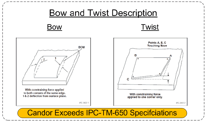
Bow refers to deviation of the PCB surface from perfect flatness resulting in either convex or concave shape. It occurs due to stresses in the board leading to outward bending. Bow is quantified as the measurement of maximum deviation from a reference plane along the length/width of the board.
Twist indicates the amount of distortion in the planar form of the PCB causing the corners to rise above or sink below the center plane. The four corners of the board are no longer coplanar due to rotational forces on the board. Twist is characterized by the maximum out-of-plane deflection between two diagonally opposite corners.
Here is an illustration depicting bowing and twisting of a PCB:
Bow and twist deformations are largely unavoidable in PCB fabrication. The aim should be to control these within acceptable limits rather than try to eliminate them fully.
Causes of Bow and Twist in PCBs
Some key factors that create stresses leading to bowing and twisting of PCBs are:
Differences in Coefficient of Thermal Expansion (CTE)
During the lamination process, the conductive copper layer, dielectric substrates and prepregs are bonded together under heat and pressure. The different expansion coefficients mean that during cooling after lamination these materials shrink by varying amounts. This creates stresses in the board leading to deformation.
Composite PCB Construction
The laminated stackup of heterogeneous materials – conductive layers, dielectric substrates, vias etc. each react distinctly to temperature and moisture. Absorption or desorption of moisture also alters dimensions differently. These combine to induce bow and twist forms.
Panel Automation Effects
PCBs are fabricated in large panels which undergo thermal and mechanical stresses during processing through conveyor ovens, copper plating tanks etc. Non-uniform stresses on the panels can result in shape distortions.
Internal Layer Misregistration
Any mismatch between position of internal layers and outer layers during lamination registration will inherently induce stresses and deformation. This effect grows with number of layers.
Plating Stresses
Significant localized stresses are generated during electrolytic copper plating which can reach over 0.5 pounds per square inch. This tends to create panel bowing and twist deformation.
Thermal Metal Deposition
During sputtering or vapor deposition of metals for surface finishing, high directional stresses occur which bend the thin panels.
Uneven Support and Tooling
During PCB panel movement between processes, uneven tooling contact or inadequate support can create flexing and distortion in panels.
Routing and scoring
Stresses induced by mechanical routing and scoring of panels to create individual PCBs from panels introduce twist and bow if not controlled.
The combination and interaction of multiple such factors during fabrication makes bow and twist very difficult to avoid completely in PCBs. Careful analysis and planning is needed to minimize them.
Problems Caused by Excessive Bow and Twist
Significant bowing or twisting shape distortion in PCBs creates several problems during manufacturing, assembly and functioning of the board which highlight the need for bow/twist control:
Reduces Assembly Yield
Excessive bow or twist will prevent proper seating of component leads in plated through holes. It hampers placement of smaller surface mount components. This directly increases assembly defects and reduces manufacturing yield.
Affects Coplanarity
Non-coplanar PCBs due to distortion interfere with mounting of quad flat packs, ball grid arrays and other devices needing flat contact pads. Solder joint stresses also increase.
Hampers Reliability
Stresses induced in solder joints and plated through holes due to board distortion negatively affect reliability of solder/PCB interconnections.
Increases Rejection Rate
Higher levels of bow and twist will fall outside permitted tolerance limits leading to rejection of fabricated PCBs. This increases cost.
Limits Panel Utilization
To counteract bowing, panel sizes may need reduction. Smaller panels mean lower PCBs per panel leading to higher cost.
Interferes Electrical Testing
Twisted boards cannot make flush contact with test fixture pins. Gaps create false failures and unreliable test results. Fixture damage can also occur.
Creates Rework Issues
Bowing and twisting results in PCBs failing during assembly process tests. This interrupts production flow and necessitates expensive rework.
Restricts Component Choices
Larger or heavier components exert greater stresses worsening deformation. Component size and weight limits may be needed.
Increases Costs
Overall PCB cost increases due to lower fabrication yields, more rework, panel size restrictions, component limitations etc.
Quantifying Bow and Twist in PCB Standards
To ensure quality and interoperability, PCB standards like IPC-A-600 provide acceptance criteria for maximum permissible bow and twist. testing methods to measure bow and twist are also defined.
Bow Measurement
As per IPC-TM-650 method 2.4.22.1, a taut wire or string is stretched across two edges of the diagonal of the PCB panel. Using a dial indicator, the maximum deviation from the reference wire is measured. This quantifies the board bow magnitude.
Twist Measurement
To measure twist as per IPC-TM-650 method 2.4.22C, two opposite corner pins stretched by rubber bands touch the PCB corners. The height difference between the other two corners indicates the degree of twist.
IPC Standards for Bow and Twist
The IPC-A-600 Acceptability of Printed Circuit Boards covers maximum permissible bow and twist in PCBs:
| PCB Thickness | Bow | Twist |
|---|---|---|
| ≤ 1.6 mm | 0.75% | 1.5% |
| 1.6 to 3.2 mm | 0.75% | 1.0% |
| ≥ 3.2 mm | 0.5% | 0.75% |
Note:
- % is based on the diagonal distance across the PCB
- Both bow and twist total should not exceed 2%
- For stiffeners and metal core boards stricter requirements apply
Techniques to Predict Bow and Twist
During the design phase itself, analysis methods help predict the bow and twist expected based on the PCB materials and layer stackup:
CLPT Analysis
Curved Beam Macromodel uses laminated plate theory to calculate thermal stress based on CTE mismatch and simulate distortion.
FEA Tools
Finite element analysis tools like Ansys, Comsol etc. can construct 3D PCB models and compute deformation under simulated process stresses.
Analytical Calculations
Manual calculations using plate theory provide approximate bow/twist values for simple geometries based on metal/dielectric thicknesses, dimensions and CTE values.
Process Modeling
Mass curing models mimic the actual curing conditions like temperature ramps, vacuum pressure etc. to forecast panel warpage.
Historical Data
Statistical regression modeling based on correlation between previously observed bow/twist values and PCB design attributes.
By predicting potential bowing and twisting early, the PCB can be optimized during design before fabrication.
Guidelines to Minimize Bow and Twist
While some bowing and twisting is unavoidable, following design and fabrication guidelines help reduce it:
Symmetric Layer Stackup
Balancing metal/dielectric layers equally about the centerline minimizes deformation due to thermal stress imbalance.
Balanced Copper Distribution
Equalizing copper densities on either side of the PCB centerline maintains symmetry and avoids bow-twist from uneven contraction.
Thinner Dielectrics
Using prepregs and bonding sheets under 100 μm thick lowers thermal stress mismatch between metal and dielectric.
Tailored CTE Dielectrics
Prepregs with CTE values between the extremes of copper and FR-4 (17 – 21 ppm/°C) produce less thermal stress and warp.
Low CTE Reinforcements
Embedding glass fabrics with very low CTE (2-5 ppm/°C) in prepregs counteracts excessive composite thermal expansion.
Low Stress Plating
Reducing plating bath stresses and operating at lower current densities lessens panel warpage from plating.
Balanced Panel Cutout
Symmetrically placed panel cutouts balance internal stresses and prevent excessive distortion.
Perimeter Support Tooling
Contact tooling around the panel edges minimizes unsupported bowing during lamination and plating processes.
Bow Reducing Routers
Routers with rigid linear motors, granite beds and linear encoders precisely score panels reducing induced stresses.
Methods of Correcting Bow and Twist
In addition to built-in panel design and process steps aimed at minimizing bow/twist, some corrective techniques are also deployed:
Panel Symmetrization
Selectively removing copper from one side and adding dielectric layers counteracts asymmetric construction causing deformation.
Stress Relieving Anneal
Post-etch bake of panels at over 180°C relieves some internal stresses induced during fabrication thereby reducing warpage.
Bow-Twist Correction Fixtures
Applying localized heat and vacuum pressure in chambers with precisely positioned industrial vacuum cups counters panel distortion.
Corner Support During Handling
Dedicated tooling with adjustable corner pins for supporting panels during handling avoids inducing bows and twists.
Panel Splicing
Cutting a large panel into smaller pieces can lower internal stresses and achieve flatter individual PCBs. But utilization suffers.
Flattening Pressing
Applying high uniform pressure between flat plates compresses top and bottom panel surfaces towards a common plane.
Mitigating Bow and Twist Effects During Assembly
While fabricating optimally flat PCB panels is ideal, somebow and twist is unavoidable. Steps can be taken during PCB population and final product assembly to mitigate issues:
Robust Component Securing
Using adhesive along with fasteners or connectors to securely fasten components like heatsinks prevents them from worsening PCB shape.
Board Stiffening
Strategically bonding stiffeners like metal strips or plastic grids on panel backsides supports flatness.
Stress Relieving Anneal
Heating fully loaded boards to over 100°C then cooling slowly in controlled fashion can relieve built-in deformations.
Selective Conformal Coating
Applying conformal coating over stressed board sections provides reinforcement against twisting or bending further.
Blanket Foam Layer
Placing foam sheet layer across backside dampens and absorbs mechanical stresses preventing distortion.
Clamping During Soldering
Using fixtures or weighted tops during reflow soldering minimizes movement and reinforces board flatness.
Panelized Assembly
Retaining PCBs in panelized format through assembly avoids introducing stresses from de-panelization.
FAQs
How are very thin and flexible PCBs tested for bow and twist?
Thin boards are tested sandwiched between metal plates to temporarily reinforce them during measurement.
Does solder masking process influence bow and twist?
Yes, poor mask adhesion or excessive mask thickness imbalance on panel surfaces can initiate or worsen bow/twist deformation.
Can soldering process induce or aggravate board warpage?
Yes, if components only loaded on one side, soldering can create asymmetric thermal stresses bowing the panel.
Is moisture absorption a factor in PCB bow and twist?
Yes, moisture absorbed by the dielectric substrate laminations causes greater expansion than copper, resulting in bowing and twisting stresses.
How to reduce bow and twist in multilayer HDI PCBs?
Use thin prepregs, symmetric spread of layers across centerline, dummy metal fills to balance densities, and selective stiffeners on panel.