What is RF Antenna? Definition, Design, Types, & Uses

5G Microstrip Antenna

An RF antenna is a device used to transmit and receive radio frequency signals. Antennas couple electromagnetic waves between free space and electronic transmitting or receiving circuitry. They provide the air interface for wireless communications, broadcasting, radar and other applications.

Below we examine how antennas work, key design parameters, different antenna types, characteristics, and typical applications where antennas are essential components.

RF Antenna Definition

An antenna is a specialized transducer that converts signals from an electronic transmission line to electromagnetic waves that propagate through space, and vice versa. Antennas couple energy between a guided wave in a conductor and an unguided electromagnetic wave in free space.

Key properties of an ideal antenna:

  • Efficiently radiates electromagnetic energy into space
  • Effectively intercepts and collects electromagnetic waves
  • Matches the characteristic impedance of connected circuitry
  • Exhibits resonant operation at the desired frequencies
  • Omnidirectional or unidirectional radiation patterns when needed
  • Rugged, resistant to environmental conditions like weather
  • Compact size while still providing adequate gain and bandwidth

In transmitting mode, an antenna converts the low voltage, high current signal from a transmission line into an electromagnetic field that detaches from the antenna and propagates through space as a radio wave.

In receiving mode, electromagnetic waves induce a voltage across the antenna, generating a small radio frequency current that is applied to the electronic receiver circuitry.

How Antennas Work

An antenna’s operation depends on the time-varying electric or magnetic fields produced by an alternating current flow through the antenna. This alternating current is generated by the connected transmitter or induced into the antenna by intercepted radio waves.

The oscillating electric and magnetic fields produced by the antenna create propagating electromagnetic waves. The nature of the fields and resulting radiation depends on the antenna geometry, driving frequency, and surrounding environment.

An antenna designed for a particular application optimizes this transformation between guided waves and free space waves. Efficiency, directionality, bandwidth, polarization and other factors are tailored for the radio link requirements.

Antenna Key Parameters & Characteristics

Below are some of the key parameters and figures of merit used to evaluate antenna performance:

  • Gain – Measure of antenna concentration of radiated power in a particular direction.
  • Directivity – Directionality of the antenna’s radiation pattern.
  • Radiation pattern – 3D spatial distribution of the antenna radiated power.
  • Bandwidth – Range of frequencies over which antenna performance is acceptable.
  • VSWR – Voltage standing wave ratio, metric of the impedance match to transmission line.
  • Return loss – Loss of signal returning/reflecting from the antenna due to mismatch.
  • Input impedance – Antenna impedance at the feed terminals or input port.
  • Efficiency – Ratio of radiated power to input power.
  • Polarization – Orientation of the antenna electric field.
  • Beamwidth – Angular width measured between half power (-3 dB) points of main lobe.

These parameters guide the process of designing and evaluating antennas for particular RF applications.

Types of Antennas

Many different antenna types and geometries exist, each with unique properties making them suitable for certain applications. Broad classifications of antennas include:

  • Omnidirectional antennas – Radiate power uniformly in all directions in a single plane. Common types are dipole and monopole.
  • Directional antennas – Focus radiation and reception in specific directions. Common types are patch, parabolic, and Yagi-Uda.
  • Aperture antennas – Open structures utilizing an aperture to enhance radiation over a large area. Common types are horn and reflector.

Antennas also employ a wide variety of feeding techniques to couple signals to/from transmission lines:

  • Direct feed – Coaxial cable attached directly to antenna.
  • Capacitive or inductive coupling – Using reactive coupling between feed line and antenna.
  • Aperture coupling – Feeding through a small slot or aperture.

Below we look at some of the most common and important types of antennas:

Wire Antennas

Wire antennas are constructed from thin metal wires usually arranged linearly or in loops. They are simple, inexpensive to construct, and lightweight.

Monopole – Single straight wire antenna with ground plane. Omnidirectional radiation pattern. Quarter-wave monopoles are most common.

Dipole – Two straight collinear wires connected centrally. Balanced structure with omnidirectional pattern. Half-wave dipoles are most common.

Loop – Wire loop or coil with maximum radiation perpendicular to the plane of the loop.

Common wire antenna configurations

Wire antennas are widely used in communications, broadcasting, instrumentation, radar and other applications. Their simplicity and omnidirectional characteristics make them suitable for many purposes.

Aperture Antennas

Aperture antennas utilize an open physical area to enhance radiation. The larger the aperture area compared to wavelength, the greater the gain and directionality.

Horn – Flared metal waveguide shaped like a horn to match wave impedance of space. Very high gain, narrow beamwidth, and broadband frequency capability.

Reflector – A dish or mirror reflecting radio waves from a primary feed antenna. Shaped to produce a directional beam for high gain performance. Used for radar, satellite, and deep space communications.

Slot – Narrow aperture cut into a metal screen. Feedline behind screen crosses aperture transversely, emitting radiation on other side.

Aperture antennas with exposed physical area to enhance radiation

Aperture antennas produce very high gain, directionality, and power handling for long range applications. The parabolic reflector is the classic high gain directional antenna.

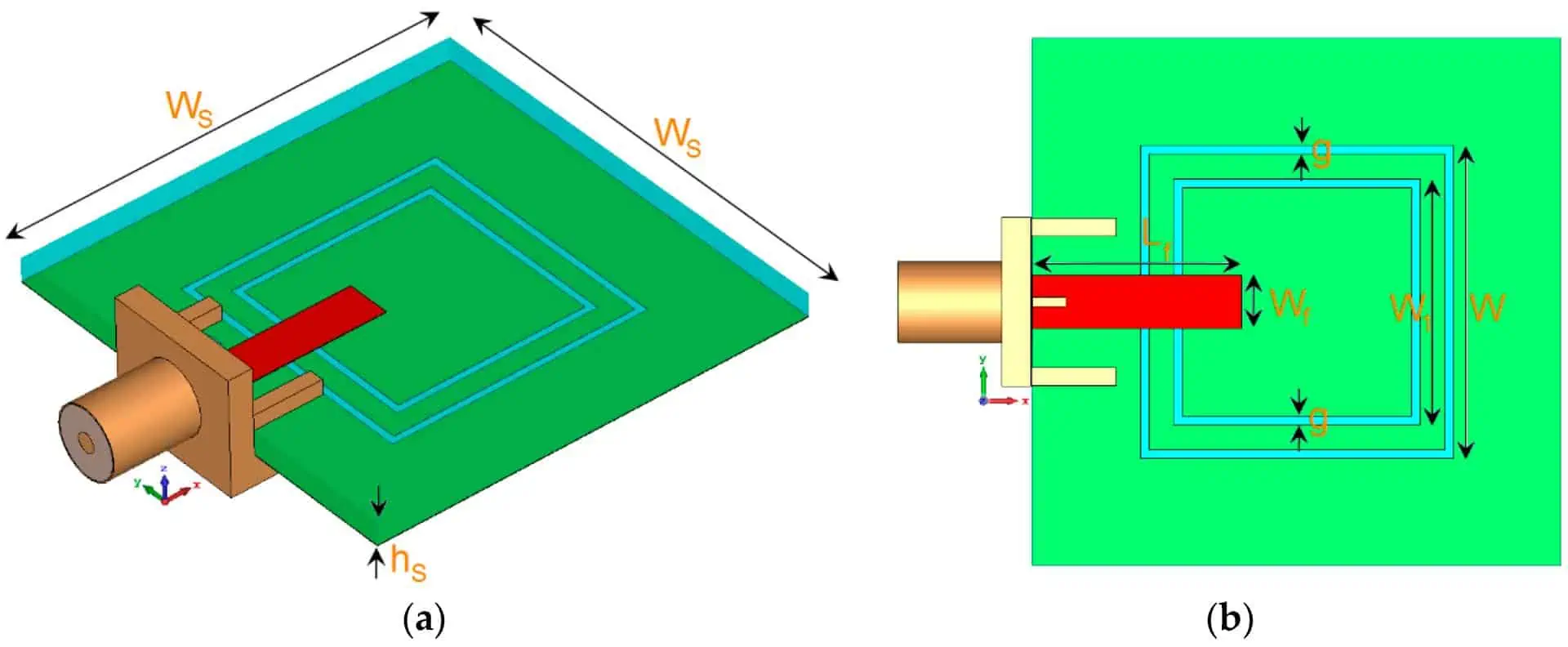
Microstrip Patch Antennas

Microstrip or patch antennas are fabricated using printed circuit board technology. They offer low-profile planar structures ideal for aerospace, mobile, and compact applications.

Patch – Square or rectangular conductive patch on top of PCB substrate, fed by a microstrip line below. Radiates perpendicular to the patch. Moderate to high gain with directional beam.

Planar inverted-F – Miniaturized patch antenna shorted on one edge using printed transmission line trace. Requires ground plane below substrate. Omnidirectional to directional patterns.

Low profile microstrip and patch antennas

Microstrip antennas allow antennas to be fabricated cost effectively as part of the electronic circuit PCB. Their compact size facilitates use in mobile and handheld wireless devices.

Array Antennas

Connecting multiple individual antenna elements together into an array provides greater control over directionality and gain:

  • Elements spaced apart at fraction of wavelength
  • Fed with equal amplitude and phase for broadside radiation
  • Corporate feed or space feed used to control pattern
  • Permits shaping of beamwidth, sidelobes, and gain

Arrays can scan electronically by shifting phase to elements or mechanically by moving entire array.

Antenna arrays combining multiple individual elements

Arraying antennas offers tremendous versatility in designing complex antenna performance characteristics.

Antenna Characteristics

Below we examine some of the key parameters and figures of merit used when designing, analyzing, and evaluating radio frequency antennas.

Radiation Pattern

The radiation pattern describes the spatial variation in radiated power density from the antenna across different directions in 3D space. Usually represented graphically in polar or rectangular plots:

3D and 2D polar plot radiation pattern of directional antenna

Analysis of the main beam lobe, sidelobes, backlobes and nulls provides insight into antenna performance.

Directivity and Gain

Directivity compares an antenna’s radiated power density in its direction of maximum radiation versus the power density from an isotropic radiator (point source).

Gain describes how much power is transmitted in the peak direction compared to the power supplied to the antenna terminals.

Gain and directivity differ by the antenna efficiency factor. Higher gain concentrates radiated power into a smaller spatial angle.

Input Impedance

Input impedance Z<sub>in</sub> is the impedance presented by the antenna at its terminals. This determines the impedance match to the connected transmission line for efficient power transfer and low reflections.

50 ohm or 75 ohm matching are common. Matching networks may adapt other impedances.

Voltage Standing Wave Ratio (VSWR)

VSWR measures the impedance mismatch between transmission line and antenna. It is the ratio of the voltage maxima to minima along the feed line. Lower VSWR values represent better antenna matching:

VSWR describes the voltage standing wave pattern caused by impedance mismatches

Typical specifications require VSWR less than 2:1 or 3:1 over the operating bandwidth.

Bandwidth

Antenna bandwidth is the range of frequencies over which performance meets specifications. Impedance match, gain, radiation pattern, polarization, and efficiency should remain within acceptable limits across the entire bandwidth.

Narrowband antennas may operate over fractions of a percent while ultrawideband antennas may achieve decades of bandwidth.

Beamwidth

Beamwidth measures angular width of the main radiation lobe, usually defined using half-power (-3 dB) points:

Beamwidth quantified using -3 dB angle off peak radiation

Narrow beamwidth concentrates radiation for high antenna directivity and gain.

Polarization

Polarization describes the orientation of the electric field component of the radio wave. Key polarizations:

  • Linear – Electric field fixed along one axis. Vertically or horizontally polarized.
  • Circular – Electric field rotates clockwise or counterclockwise with propagation. Used in satellite communications.
  • Elliptical – Electric field rotates elliptically in the plane perpendicular to propagation. General case of circular polarization.

Various electromagnetic wave polarization types

Polarization is an important antenna property matching receivers to transmitted waves.

Antenna Efficiency

Efficiency metrics quantify how much power delivered to the antenna is actually radiated as electromagnetic waves:

Radiation efficiency – Ratio of radiated power to total accepted power

Total efficiency – Ratio of radiated power to net input power

Losses such as I^2R heating, dielectric absorption, and impedance mismatches reduce efficiency below 100%. Highly efficient antennas minimize internal losses and maximize radiated power.

Typical Antenna Applications

Antennas enable wireless connectivity, broadcasting, sensing and observation across the radio spectrum:

  • Communications – Connecting cell phones, WiFi devices, Bluetooth headsets, emergency radios, and other electronic systems wirelessly. Antennas are embedded or external.
  • Broadcasting – Transmitting radio, television, satellite TV and mobile audio programming to individual receivers and cell sites. High gain outdoor antennas used.
  • Radio astronomy – Large specialized antennas like Arecibo and Very Long Baseline Arrays gather faint cosmic microwave signals for scientific observation.
  • Radar – Detecting objects by analyzing reflected EM waves. Directional high gain antennas required for long range radar. Used for air traffic control, meteorology, and target tracking.
  • Satellite – Parabolic dish antennas transmit and receive signals over huge distances to communicate with Earth orbiting satellites for data, video, telephony, and military uses.
  • RFID – Small antennas in UHF or microwave bands transfer data to/from RFID tags for item identification and tracking.
  • Medical – RF and microwave signals applied in body imaging techniques including MRI and diathermy therapeutic tissue heating.

These key applications demonstrate the indispensable role antennas play in any system involving transmission, reception or interaction with electromagnetic waves across the radio spectrum.

Frequently Asked Questions

  1. What is an antenna?

An antenna is a device used to transmit and receive radio frequency signals by converting electromagnetic waves in space to electrical currents and vice versa. They provide the air interface for wireless communications.

  1. What are the key properties of an antenna?

Important antenna parameters are gain, directivity, radiation pattern, impedance, bandwidth, VSWR, beamwidth, polarization and efficiency. These determine suitability for particular applications.

  1. What are the main types of antennas?

Common antenna types include wire antennas like monopoles and dipoles, aperture antennas like horns and dishes, microstrip patch antennas, and antenna arrays combining multiple elements.

  1. How does an antenna concentrate radiated power?

By focusing the emitted electromagnetic waves in a particular direction, an antenna concentrates signal power into a narrow solid angle for increased gain and directivity.

  1. What applications use antennas?

Antennas are essential components enabling technologies including communications, broadcasting, radar, radio astronomy, satellite links, RFID, medical RF, and any application involving transmission/reception of radio waves.

What Is IoT (Internet of Things)? Definition, Types, Technologies and Applications

IoT Devices

What is IoT?

IoT stands for Internet of Things. It refers to the network of physical objects embedded with sensors, processing ability, software and other technologies that connect and exchange data over the Internet or other communications networks.

IoT enables objects to be sensed and controlled remotely over the existing network infrastructure creating opportunities for direct integration of physical world into computer systems. This allows improving efficiency, accuracy and economic benefit in addition to reduced human intervention.

The IoT concept builds on the proliferation of smart devices like smartphones, tablets, sensors and connected vehicles that collect and transmit data via the internet. When objects can represent themselves digitally, they can be controlled from anywhere.

Some key aspects of the IoT include:

  • Physical objects with embedded technology to interact and communicate
  • Network connectivity to share data and remote control
  • Internet protocols, standards and architecture
  • Intelligent data analytics and algorithms

A Simple IoT Example

A simple example of an IoT system is a smart home, where devices and appliances are connected to a network and can be remotely monitored and controlled:

  • Smart thermostat automatically adjusts temperature and optimizes heating/cooling energy costs
  • Smart lighting adjusts LED brightness based on time of day and occupancy
  • Smart locks allow remote control of door locks via smartphone
  • Smart appliances communicate usage data to optimize electricity utilization
  • Security cameras provide alerts and remotely stream video
  • Smoke/CO detectors send instant alerts to phones in emergency

All these connected devices collect data, relay commands, and enable remote control through internet connectivity. IoT enables new levels of efficiency, automation and responsiveness.

IoT Definition

IoT can be defined as:

โ€œA system of interrelated computing devices, mechanical and digital machines provided with unique identifiers (UIDs) and the ability to transfer data over a network without requiring human-to-human or human-to-computer interaction.โ€

Key aspects of this definition include:

  • Computing Devices – Embedded systems with processing, memory and network connectivity. Can include edge devices or cloud servers.
  • Mechanical/Digital Machines – Smart objects with sensors, actuators and software. Allows physical world interfacing.
  • Unique Identifiers – Addressability of each object within the IoT system, like an IP address. Allows unified data coordination.
  • Data Transfer – Objects autonomously exchange data facilitating remote monitoring and control reducing human intervention.
  • Network Connectivity – Leverages existing internet infrastructure enabling connectivity.

This represents the essence of the IoT concept – enabling intelligent, interconnected ecosystems of technology to automate tasks and augment human capabilities.

RAYMING 4 Layer IoT Household air purifier PCB

RAYMING 4 Layer IoT Household air purifier PCB

Original price was: $19.00.Current price is: $18.50.

Product name: 4-layer Internet of Things PCB boards Board Material: TU-662 Thickness: 1.6mm Layer Number๏ผš4 layers PCB Minimum line width/spacing: 6/6mil Finished copper thickness: inner layer 2OZ, outer layer 2OZ Acceptance standard: IPC6012 CLASS 2 level Surface technology: lead-free HASL Dielectric constant: 4.3 Loss factor: 0.014 Usage: Household air purifier   4 Layer IoT Household…

Brief History of IoT

The Internet of Things as a concept has evolved over several decades:

  • 1970s – Early internet protocols like TCP/IP were developed enabling internetworking
  • 1990s – As more devices were connected, the term โ€œubiquitous computingโ€ was coined to describe the prevalence of computing
  • 1999 – Kevin Ashton coined the phrase โ€œInternet of Thingsโ€ to describe a system where objects in the physical world could be connected to the internet.
  • Early 2000s – RFID and wireless sensor networks emerged as enabling technologies. Focus on machine-to-machine communications.
  • 2008 – The number of connected devices exceeded the human population.IoT concept gained popularity.
  • 2009 – Number of internet connected objects surpassed the number of computers on the internet.
  • Present Day – Billions of devices now connected forming a global network. IoT continues to expand into many application domains.

We now live in a hyper-connected world with billions of devices interconnected and exchanging data. IoT has moved from concept to reality.

IoT System Architecture

A generic IoT system architecture consists of:

1. Physical Layer

Composed of embedded devices with sensors and actuators to interface with the real world. Includes smart wearables, appliances, industrial machines, vehicles, and more.

2. Network Layer

Provides connectivity and communications using protocols like WiFi, Bluetooth, LPWAN, cellular, satellite, etc. Can include gateways and routers.

3. Edge Computing Layer

Distributed intelligence in the form of real-time analytics and processing at the edge of the network rather than relying solely on the cloud. Often uses embedded systems or micro data centers.

4. Platform Layer

Central hubs that aggregate, process, analyze and disseminate data. Provides management, security and data storage. Cloud platforms or on-premise servers.

5. Application Layer

Human interaction with the IoT system using apps and visualization. Enables monitoring, remote control, analytics, dashboards, etc.

This provides a framework to understand the core technology components that enable an IoT ecosystem. Different architectures can vary based on the specific use case.

IoT Enabling Technologies

IoT devices raspberry pi

Several key technologies have converged to enable the Internet of Things:

  • Sensors – MEMS accelerometers, gyroscopes, temperature sensors, pressure sensors, etc that interface with the physical environment.
  • Actuators – Motors, servos, valves, switches and more that provide physical motion or control.
  • Smart Devices – Powerful embedded systems like microcontrollers, System on Chips, Single Board Computers that enable local processing.
  • Communication – Wireless networking technologies like WiFi, Bluetooth, LoRaWAN, NB-IoT, LTE-M and 5G provide connectivity.
  • Identification – RFID tags, barcodes, cameras enable identifying and tracking objects.
  • Location – GPS, cellular, WiFi triangulation enables location tracking capabilities.
  • Power – Battery technology, energy harvesting and wireless charging enable untethered operation.
  • Data Analytics – Analytics algorithms extract insights from sensor data streams using techniques like machine learning and AI.
  • Cloud/Fog Computing – Cloud platforms provide data aggregation, processing, visualization and storage. Fog/edge computing enables some decentralized processing.
  • Network Protocols – Networking standards like TCP/IP allow objects to communicate over the internet infrastructure.

The maturity and ubiquity of these technologies has allowed the IoT concept to move beyond hype into mainstream adoption.

IoT Connectivity Protocols and Standards

For IoT ecosystems to function efficiently, connected devices and systems need to speak a common language. A variety of protocols, network architectures and standards enable devices to communicate:

TCP/IP – Transmission Control Protocol / Internet Protocol that provides addressing scheme along with reliable transmission of data packets between internet connected devices.

6LoWPANIPv6 over Low Power Wireless Personal Area Networks. Enables IP-based communications for low power devices like sensors.

MQTT – Message Queuing Telemetry Transport lightweight publish-subscribe messaging protocol well suited for IoT devices.

AMQP – Advanced Message Queuing Protocol for queuing and routing enterprise messages between clients.

CoAP – Constrained Application Protocol, a web transfer protocol designed for low power devices.

LWM2M – Lightweight M2M protocol from OMA for managing IoT/M2M device services.

LoRaWAN – Long Range Wide Area Network protocol for low power wide area networks.

DDS – Data Distribution Service real-time middleware protocol from Object Management Group.

OPC-UA – Open Platform Communications Unified Architecture standard for industrial automation.

oneM2M – Global M2M/IoT standard that enables interoperability across multiple industries and domains.

Adherence to common protocols and standards ensures interoperability between diverse systems and allows them to exchange data.

IoT Security Challenges

With billions of connected devices, IoT systems pose unique security challenges:

  • Weak default passwords on devices
  • Lack of encryption on data communications
  • Insecure network interfaces
  • No secure hardware storage
  • Lack of physical hardening
  • Infrequent security patch updates
  • Exploitable software bugs
  • Large unmonitored attack surface

This can lead to cyberattacks against IoT networks like:

  • Botnets controlling swarms of devices
  • Leaked personal data from wearables or smart homes
  • Safety critical manipulations like vehicle brake overrides
  • Ransomware attacks that disable systems
  • Privacy violations from sensor data leaks
  • Data integrity loss from malicious data manipulation

IoT security issues can undermine consumer confidence in the technology and pose major risks to individuals and organizations. Securing IoT ecosystems remains an ongoing challenge and priority.

IoT Design Principles

5G IoT Technology

To architect effective and secure IoT systems, key principles include:

  • Simplicity – Avoid unnecessary complexity in design to minimize vulnerabilities. Use compact protocols optimized for IoT.
  • Resiliency – Build in backup mechanisms in case of outages. Assume unreliable network connectivity. Design for occasional power loss.
  • Modularity – Reusable, interoperable components and interfaces improve flexibility and maintenance. Design for piecewise updates.
  • Statelessness – Avoid retaining excessive state or session information that may be lost. Design stateless interfaces when possible.
  • Redundancy – Critical systems should have fail-over mechanisms with redundant components.
  • Heterogeneity – Design for multiple platforms, operating systems, and generations of technology.
  • Security – Consider security from the ground up rather than an afterthought. Utilize encryption, authentication, validation, monitoring and other security measures.

Adhering to these design tenets can help create robust and secure IoT ecosystems.

IoT Design Considerations

Here are some key considerations when architecting an IoT system:

  • What sensors and data need to be collected?
  • How will devices communicate and connect to networks?
  • What protocols will devices use to exchange data?
  • How much processing needs to occur at the edge versus cloud?
  • What user interfaces and visualization are needed?
  • How will captured data be analyzed and utilized?
  • What security features will be implemented end-to-end?
  • How will system health, logs and data be monitored?
  • How will devices be remotely managed and updated?
  • How will system scale and expand in the future?

Thoroughly evaluating technical capabilities, security, lifecycle management and scalability are critical when designing IoT ecosystems.

Types of IoT Devices

There are a multitude of physical devices that comprise the IoT. Below are some major categories:

Consumer IoT Devices

  • Smart home devices – thermostats, cameras, appliances, lighting, locks
  • Wearables – smart watches, fitness trackers, medical devices
  • Entertainment – smart TVs, streaming devices, VR headsets
  • Smartphones and tablets
  • Vehicle telematics for tracking, maintenance

Industrial IoT Devices

  • Sensors – temperature, pressure, flow, level, gas
  • Motor controllers, pumps, valves
  • Fabrication machinery, robots, conveyors
  • Asset and environment monitoring
  • Logistics and fleet tracking devices

Medical IoT Devices

  • Wearable monitors – pulse oximeter, heart rate, blood pressure
  • Implantable devices – pacemaker, glucose monitor, neurostimulator
  • Portable health equipment – ventilator, infusion pump
  • Remote patient monitoring systems

Retail and Supply Chain IoT Devices

  • Smart shelves with RFID/barcode scanning
  • Inventory robots
  • Smart carts for shopping analytics
  • Supply chain trackers – pallets, containers, packages

Smart City IoT Devices

  • Air quality monitors
  • Noise detection sensors
  • Smart electric/gas/water meters
  • Streetlights, traffic lights
  • Parking sensors and guidance systems
  • Traffic management sensors

This demonstrates the incredibly diverse range of devices that can be networked and automated through IoT implementations.

IoT Implementation Challenges

embedded iot

Some key challenges faced when implementing IoT projects:

Complexity – Vast number of protocols, technologies, vendors and choices leads to complex integrations.

Security – Securing billions of devices and data with constrained resources presents extreme challenges.

Privacy – Personal data collection can raise privacy concerns demanding transparency and consent.

Legacy Integration – Integrating with legacy enterprise systems can be difficult and require middleware.

Data Management – Collecting, organizing, analyzing huge volumes of time series IoT data.

Costs – Sensors, network access, cloud services and personnel add up quickly.

Power – Providing consistent power to a mesh of wireless battery-operated devices.

Interoperability – Lack of common standards can lead to isolated vertical solutions.

Uncertainty – Hard to predict and account for technology evolution over decades long deployments.

A systematic approach is required to address these barriers and successfully deliver IoT solutions.

IoT Application Domains

IoT use cases span across nearly every industry and domain including:

Smart Cities

  • Traffic monitoring and adaptive control
  • Smart lighting and energy usage
  • Air quality and pollution monitoring
  • Noise mapping
  • Water distribution and leakage monitoring
  • Waste management optimization
  • Public safety and crowd control

Industrial IoT

  • Predictive maintenance of machinery
  • Asset management and tracking
  • Fleet vehicle telematics and routing
  • Supply chain and logistics optimization
  • Safety monitoring – gas, chemicals, temperature
  • Energy usage monitoring and correlation
  • Inventory management

Consumer IoT

  • Smart homes – appliances, security, lighting
  • Quantified self wearables for health and fitness
  • Pet monitoring and tracking
  • Elderly monitoring and assistance
  • Smart retail analytics
  • Context-aware mobile devices like phones

Transportation IoT

  • Real-time traffic alerts and routing
  • Autonomous vehicles
  • Vehicle telematics and diagnostics
  • Usage-based insurance (UBI)
  • Airport and cargo transport tracking and optimization
  • Railroad infrastructure monitoring
  • Charging infrastructure optimization

Healthcare IoT

  • Remote patient monitoring and telehealth
  • Wearables for fitness tracking and elderly care
  • Asset management and tracking – equipment, files
  • Patient flow optimization and ER automation
  • Medication tracking and adherence
  • Environmental monitoring – temp, humidity

Energy IoT

  • Smart grid optimization and automation
  • Renewables management – solar, wind
  • Predictive maintenance on generators and turbines
  • Leakage detection for gas lines or water pipes
  • Outage detection and restoration confirmation
  • Usage monitoring and analytics

Agriculture IoT

  • Smart farming – automated irrigation, pH monitoring
  • Livestock tracking and bio-surveillance
  • Cold storage and supply chain monitoring
  • Soil moisture optimization
  • Predictive analytics for crop yield
  • Self-driving tractors

This illustrates just some of the diverse application domains that IoT is revolutionizing by connecting the physical world.

IoT Application Examples

Here we will examine some specific IoT applications:

Smart Factory

In manufacturing, IoT enables the smart factory for process optimization:

  • Machines – networked for monitoring predictive maintenance, reducing downtime
  • Inventory – RFID/barcode for tracking parts through processes
  • Environment – sensors monitor temperature, humidity, air particles
  • Personnel – wearables for location, safety alerts
  • Vehicles – autonomous transport between stations
  • Quality – computer vision systems perform inspections
  • Control – integrate processes into coordinated workflows

IoT unlocks huge potential efficiency and cost improvements in manufacturing.

Smart Agriculture

IoT transform farming through precision data:

  • Soil – probe moisture levels optimize watering
  • Equipment – monitor usage and diagnostic codes
  • Livestock – wearables track location and health
  • Crops – drones and aerial imagery for precision treatments
  • Climate – weather monitoring guides planting and harvesting
  • Storage – monitor grain temperature and humidity

IoT enables massive improvements in crop yields and sustainability.

Wearable Health Monitoring

Wearables allow continuous health monitoring:

  • Fitness – track steps, calories, sleep, heart rate
  • Fall detection – detect falls and automatically call for help
  • Chronic care – monitor glucose, blood pressure, oxygenation
  • Rehabilitation – track usage and progress of home exercises
  • Clinical trials – real-world data on medications and effectiveness

IoT wearables provide data enabling better health decisions.

Smart Retail

Retail IoT applications:

  • Checkout – mobile POS speeds checkout
  • Inventory – RFID tracks inventory in real-time
  • Location – in-store location powers personalized offers
  • Customer Analytics – camera analytics determine demographics
  • Digital Signage – dynamically change displayed ads
  • Loss Prevention – sensors detect shoplifting attempts

IoT gives retailers better visibility into operations and customers.

This illustrates just a few examples of innovative IoT implementations across industries. The possibilities are endless.

The Future of IoT

IoT has immense potential for the future as more objects become digitally connected and share data:

  • Tens of billions more devices will join the IoT ecosystem with continued cost declines in hardware.
  • Advances in low power wireless networking like 5G and LPWAN will enable wider connectivity.
  • Trend toward distributed cloud and edge computing will drive analytics closer to IoT devices.
  • Improved security and standardization will increase trust and interoperability.
  • Development of blockchain and DLT may add decentralized mechanisms for identifier and data sharing.
  • More ambient intelligence will evolve decision making towards autonomy.
  • Growth of augmented reality and brain-computer interfaces will drive immersive control.
  • Machine learning and AI will enable more predictive capabilities from sensor data.

The IoT revolution is still just beginning as it promises to enhance nearly every aspect of life and industry.

What is Embedded System Hardware: Types, Design and Development Process

Introduction

Embedded systems are microcontroller or microprocessor based systems designed to perform dedicated functions within larger mechanical or electrical systems. Embedded system hardware refers to the electronic components and devices which make up the embedded system and enable its functioning.

This article provides an in-depth look at embedded system hardware including:

  • Major components and devices used
  • Hardware architectures and configurations
  • Design considerations and selection criteria
  • Hardware/software partitioning
  • Development and testing process
  • Industry applications

Understanding the embedded hardware landscape is crucial for successfully designing and developing embedded products and solutions across consumer, industrial, medical, automotive, aerospace and other segments.

Embedded System Hardware Components

An embedded system consists of both hardware and software elements configured and integrated together on typically a printed circuit board to deliver the desired functionality. The key hardware components include:

Microprocessor/Microcontroller

This is the central processing unit and “brain” of the embedded system. Popular options:

  • Microcontrollers โ€“ Integrated CPU with memory, I/O, peripherals
  • Microprocessors โ€“ Standalone general purpose CPU requiring external chips
  • Common architectures: x86, ARM, AVR, PIC, 68k, MIPS, PowerPC

Memory Devices

Used to store the executable program code, data and instructions required for the system to function:

  • Volatile Memory โ€“ SRAM, DRAM lose data when power is removed
  • Non-Volatile Memory โ€“ Flash, EEPROM retain data without power
  • Amount of memory depends on software needs

I/O Interfaces

Allow the processor to receive inputs and drive outputs:

  • Parallel interfaces โ€“ PCI, SCSI
  • Serial interfaces โ€“ UART, SPI, I2C, USB
  • Wireless โ€“ Bluetooth, Wi-Fi, Zigbee
  • Analog to Digital Converters (ADCs)
  • Digital to Analog Converters (DACs)

Power Supply

Provides regulated voltages to run the electronics:

  • Linear regulators โ€“ Low noise but less efficient
  • Switching regulators โ€“ More efficient but with switching noise
  • Supervisory circuits โ€“ Reset generation, brown-out protection
  • Backup supply โ€“ Batteries or capacitors

Clock Generation

Produces clock signals to synchronize operations:

  • Crystal oscillators
  • Phase locked loops (PLLs)
  • Real time clocks (RTCs) with backup

Custom Circuits

Application specific standard products (ASSPs), field programmable gate arrays (FPGAs) and other components tailored for embedded use.

Hardware Architectures and Platforms

Embedded PCB

Embedded system hardware can be architected in different ways based on technical requirements and tradeoffs:

Single Chip Architecture

  • All functionality integrated within a microcontroller IC
  • Simplest approach
  • Constrained by on-chip capabilities
  • Examples: SmallInstrumentation, IoT sensors

Microprocessor with Discrete Chips

  • Microprocessor coupled with peripherals and interfaces
  • More hardware flexibility
  • Complex board design
  • Obsolescence management challenges
  • Widely used in industrial, medical, automotive products

System on Chip (SoC)

  • Multiple functions integrated together on a single IC die
  • Highest performance and integration
  • Longer development timeframes
  • Typical in smartphones, gaming consoles, robots

System on Module (SoM)

  • Functional blocks implemented together on a small board/module
  • Allows customization
  • Simplifies development
  • Growing approach for industrial automation, gateways

System in Package (SiP)

  • Multiple ICs enclosed in a single package
  • Reduces size, cost, power
  • Limited reconfigurability
  • Used where miniaturization is critical

Choosing the right architecture involves tradeoffs between technical needs, timeline, costs, reusability, and other product requirements.

Design Considerations

Key hardware design criteria and considerations for embedded systems:

Processing Power

  • Analysis of software tasks to gauge MIPS/DMIPS required
  • Headroom for future features/performance
  • Selection of optimal micro architecture

I/O Needs

  • Interfaces for all sensors, actuators, peripherals
  • On-chip vs external options
  • Analog vs digital interfaces

Memory Requirements

  • Flash, RAM needs based on software
  • Expansion capability
  • Reliability, endurance factors

Power Requirements

  • Source voltage/current specifications
  • Backup/battery needs
  • Power saving modes

Physical Constraints

  • Size, weight limitations
  • Environmental factors
  • Mechanical integration needs

Reliability Requirements

  • Component ratings and lifespans
  • Redundancy needs
  • Ruggedization
  • Heat dissipation

EMI/EMC Considerations

  • Shielding
  • Filtering
  • Isolation
  • Minimal radiated/conducted emissions

Compliance Requirements

  • Safety, regulatory standards
  • Certifications

Budgetary Constraints

  • BOM cost targets
  • Non-recurring engineering (NRE) costs

Making appropriate hardware choices requires carefully weighing these factors.

Component Selection Process

embedded iot

Choosing the right components is key to building optimized embedded systems. The selection process involves:

Defining Technical Needs

  • Processing performance specifications
  • Memory and storage needs
  • I/O interfaces and peripherals required
  • Power budgets
  • Physical form factors
  • Life expectancy and use conditions
  • EMI/EMC requirements
  • Other technical requirements derived from product specs

Evaluating Options

  • Review potential component choices from reputable suppliers
  • Compare technical capabilities to identify devices that fulfill needs
  • Get samples for evaluation if required
  • Assess development tools and OS/software support
  • Review technical datasheets in detail

Analysis and Decision Factors

  • Make components choices based on how closely they meet technical requirements
  • Evaluate cost impact (unit cost, BOM cost)
  • Consider availability, lifecycle, obsolescence risks
  • Assess development effort needed (drivers, firmware, tools)
  • Analyze power consumption tradeoffs
  • Consider previous experience and expertise with components
  • Take inputs from procurement team

Final Component Selection

  • Select optimal components for each system function based on analysis
  • Ensure all design requirements are fully met
  • Validate choices via prototype evaluations
  • Lock down part numbers, suppliers, procurement specs early
  • Formalize technical datasheets for chosen components
  • Setup lifecycle monitoring in case of obsolescence risks

Getting components selection right from the start prevents extensive redesigns later and leads to better performing, compliant, and cost-effective embedded products.

Hardware and Software Partitioning

Determining which functions to implement in hardware vs software is a key partitioning decision:

Hardware Implementation

  • Provides better performance, speed
  • Hard to modify or upgrade post-production
  • Suited for time-critical functions
  • Examples: real time I/O, complex processing

Software Implementation

  • More flexible, easier to change
  • Simplifies upgrades/bug fixes
  • Better for non-real time tasks
  • Examples: application logic, UI, network stacks

Partitioning Guidelines

  • Implement timing critical functions in hardware
  • Keep hardware as simple as possible
  • Use software for higher level tasks
  • Consider upgrade needs during product lifecycle
  • Leverage hardware accelerators where possible
  • Evaluate CPU load and memory bandwidth needs
  • Maintain balance โ€“ don’t over burden hardware or software

Well planned partitioning allows focusing hardware on key strengths like speed, while software manages evolving functionality over time.

Embedded Hardware Design Process

Developing optimized embedded system hardware requires progressing through a structured design flow:

Requirements Analysis

  • Capture detailed hardware requirements and specs
  • Cover functionality, performance, reliability needs
  • Input from electrical, mechanical, software teams
  • Account for use cases, edge conditions
  • Define project deliverables

System Architecture

  • Translate requirements into high-level system architecture
  • Block diagrams showing key hardware elements
  • Hardware/software partitioning
  • Interface definitions
  • Input/Output detail

Component Selection

  • Choose most appropriate components matching requirements
  • Microprocessor/microcontroller
  • Peripherals, external interfaces
  • Memory devices
  • Oscillators, crystals

Circuit Design

  • Design supportive circuits for power, reset, clocking
  • I/O signal conditioning
  • Protection against faults, transients
  • EMI/EMC control measures
  • High speed PCB layout considerations

Prototyping

  • Create prototype PCB layout for evaluation
  • Assemble prototype using chosen components
  • Write basic test firmware for functionality validation
  • Iterate on design based on lab tests, debug data

compliance Testing

  • Test prototype against complete requirements
  • Address any gaps or issues observed
  • Confirm compliance with applicable standards
  • Iterate until all criteria are met

Documentation

  • Comprehensive datasheet detailing hardware design
  • Block diagrams, schematics, PCB layout data
  • Component technical specs, BOM
  • Compliance reports

Production Release

  • Finalize design for volume production
  • Quality checks to ensure reproducible builds
  • Release to manufacturing with comprehensive documentation

This structured hardware design flow is key to avoiding costly mistakes and building robust, compliant embedded systems.

PCB Design and Layout

Embedded Hardware Engineer

The printed circuit board (PCB) physically houses the embedded components and interconnects them together via copper traces. Good PCB design is critical for reliability. Key aspects include:

Schematics

  • Detailed schematics with component symbols, values, and labels
  • Schematic-PCB cross probing for easy navigation
  • Adherence to industry standards

Component Placement

  • Group related circuits together
  • Ensure serviceability around key components
  • Optimize for manufacturability

Routing

  • Use appropriate trace widths for signals
  • Provide adequate clearances
  • Include ground and power planes
  • Control impedance for high speed traces
  • Minimize length of high current paths

EMI/EMC Control

  • Enclose circuits in ground planes
  • Include filtering components
  • Careful use of spacing, stitching vias
  • Controlled impedances

Thermal Management

  • Ensure component temperature limits are not exceeded
  • Use thermal relief cutouts, thermal vias
  • Specify appropriate surface finishes

Mechanical Integration

  • Mounting holes, brackets, specialty connectors
  • Clearance for fixtures/housings
  • Shock/vibration resistance measures

Investing in optimal PCB design upfront avoids expensive re-spins later and leads to rugged, reliable embedded hardware.

Embedded Hardware Testing

Embedded Hardware Engineer

Thorough testing across unit, subsystem, and system levels is crucial for validating embedded hardware designs:

Component Level Testing

  • Confirm electrical performance of individual ICs
  • Stress tests for endurance, lifecycle estimation
  • Benchmark to datasheet parameters

Subsystem Validation

  • Focused testing of specific circuits (I/O, power, clocking, communications)
  • Verify conformance to multi-year lifetime under use conditions
  • Characterize EMI, power consumption

System Level Integration Testing

  • Validation of fully populated PCB assembly
  • Stress testing system level reliability โ€“ thermals, vibration…
  • Functional testing with production ready software
  • Compliance verification to standards

Product Level QA

  • Testing in actual end product enclosures
  • User environmentals โ€“ temperature, humidity, shock…
  • Lifecycle testing โ€“ thermal cycling, HALT, reliability simulations
  • Final validation of all requirements

Continuous testing at increasing levels of assembly ensures the hardware design and production processes achieve the reliability metrics mandated for the product.

Applications of Embedded Hardware

Embedded hardware spans a diverse range of applications across industries:

Industrial Automation

  • Programmable Logic Controllers (PLCs)
  • Human Machine Interface (HMI) terminals
  • Process transmitters, field instruments
  • Motor drives, robotics

Medical Equipment

  • Diagnostic imaging systems
  • Patient monitoring systems
  • Infusion pumps, ventilators
  • Surgical robots, prosthetics

Building Automation

  • Smart energy meters
  • Lighting, HVAC, access control systems
  • Fire alarm systems
  • Video intercoms, security systems

Transportation

  • In-vehicle infotainment
  • Advanced driver assistance systems (ADAS)
  • Railway signal control
  • Aircraft flight systems, black boxes

Consumer Electronics

  • Home automation systems
  • Smartphones, tablets, smart watches
  • Gaming consoles
  • Digital cameras

Energy

  • Smart grid sensors and automation
  • Solar micro-inverters
  • UPS systems
  • Oil and gas instrumentation

Whether enabling smarter factories, autonomous vehicles, or IoT connectivity โ€“ embedded hardware delivers the core electronics in millions of products we use daily across industries.

Conclusion

Embedded system hardware provides the underlying electronics comprising the processing, communications, user interfaces, and control capabilities in dedicated devices. Well designed embedded hardware is vital for reliably and securely running the software driving intelligent behavior in connected systems.

A methodical approach to hardware selection, partitioning, prototyping and testing enables the development of optimal PCB assemblies despite severe constraints. As embedded technology expands into AI, industrial IoT, robotics, and other fields โ€“ robust, high performance hardware remains essential for unlocking next generation innovations.

Frequently Asked Questions

Here are some common questions about embedded system hardware answered:

Q: What are the main hardware components in an embedded system?

A: The core hardware components include the CPU (microprocessor or microcontroller), memory devices, I/O interfaces, power supply, clocks, and custom ICs/accelerators tailored for the application.

Q: How is hardware/software partitioning done?

A: Time critical functions are implemented in hardware for performance while higher level application logic and networking layers are partitioned to software for flexibility.

Q: What are the main steps in the embedded hardware design process?

A: The main steps include – requirements analysis, system architecture, component selection, circuit design, prototyping, testing, documentation, and production release.

Q: What are some key considerations in embedded hardware design?

A: Key considerations include – processing power, I/O needs, memory requirements, power budgets, physical constraints, reliability, standards compliance, EMI/EMC, thermal management, and cost.

Q: How is PCB layout optimized in embedded systems?

A: Good PCB layout focuses on schematic-board correlation, optimal component placement, controlled routing, thermal management, and EMI/EMC control measures for reliability.

What is Raspberry Pi 5 tablet?

Overview of the Raspberry Pi 5

The Raspberry Pi 5 is the latest model in the popular Raspberry Pi series of single-board computers. While previous Raspberry Pi devices have been credit card-sized boards designed for hobbyists and educators, the Pi 5 represents a major evolution – it is Raspberry Pi’s first tablet computer.

The Raspberry Pi Foundation unveiled the Pi 5 in early 2023. It features a touchscreen display, built-in battery, and new quad-core processor, allowing it to function as a standalone tablet device without being connected to peripherals. However, it retains the GPIO pins and capabilities of a Raspberry Pi board, enabling hobbyist projects.

Raspberry Pi Compute Module 4 - 8GB RAM, 32GB eMMC, 2.4/5.0GHz Wi-Fi & Bluetooth 5.0

Raspberry Pi Compute Module 4 – 8GB RAM, 32GB eMMC, 2.4/5.0GHz Wi-Fi & Bluetooth 5.0

Original price was: $98.00.Current price is: $95.00.

This version of the Raspberry Pi Compute Module 4 includes a high-performance 64-bit quad-core processor, 8GB LPDDR4 RAM, 32GB eMMC, dual-display support at resolutions up to 4K, hardware video decode at up to 4Kp60, Gigabit Ethernet, USB 2.0, dual camera interfaces, PCIe Gen 2 x1 interface, and dual-band 2.4/5.0GHz wireless LAN and Bluetooth 5.0.

SKU: RAYMING20240527001
Category:

Key Features of the Raspberry Pi 5

  • 7 inch IPS touchscreen display
  • Quad-core ARM processor
  • 4GB RAM
  • 64GB storage
  • 802.11ac WiFi & Bluetooth 5.0
  • USB-C port for power input and data transfer
  • 40-pin GPIO header for electronics projects
  • Lightweight tablet form factor with sturdy casing
  • Runs Raspberry Pi OS software

With its tablet-focused design, the Pi 5 opens up new possibilities for Raspberry Pi users. It can function as a portable computer for programming, web browsing, and office tasks. The touchscreen makes it ideal for interactive GUI projects. It also works well as an entertainment device for games, videos, and ebooks.

Hardware Specifications

Here are the key hardware specifications for the Raspberry Pi 5 tablet:

ComponentSpecification
ProcessorBroadcom BCM2711C0 quad-core Cortex-A72 64-bit SoC @ 1.5GHz
RAM4GB LPDDR4 SDRAM
Storage64GB eMMC flash storage
Display7″ IPS touchscreen, 720p resolution
Camera5MP rear camera
Wireless802.11ac WiFi, Bluetooth 5.0
USB1x USB 3.0 Type-C
GPIO40-pin header, supports Raspberry Pi HATs
Battery8000mAh lithium-polymer, up to 8hrs life
Dimensions197 x 115 x 10mm
Weight370g

The Pi 5’s quad-core ARM processor gives it significantly more processing power than previous Pi boards. The 4GB of RAM also makes it capable of running more intensive applications.

The 64GB of onboard storage provides ample space for the operating system, software, media files, and project data. A microSD card slot allows further expansion.

The 7-inch touch display has 720p resolution, making it sharp and responsive. The rear 5MP camera enables computer vision projects.

For connectivity, it has the latest WiFi and Bluetooth specs, along with a USB-C port for data and power. The 40-pin GPIO header gives full access to Raspberry Pi’s digital interfaces.

The 8000mAh battery enables up to 8 hours of use for a fully portable experience. The tablet itself has a durable casing and is compact at just 10mm thick.

Software and Operating System

The Raspberry Pi 5 comes pre-installed with the official Raspberry Pi OS software. This Debian-based Linux distribution is optimized for Raspberry Pi hardware.

Key software included:

  • Desktop environment with app launcher, taskbar, file manager
  • Chromium web browser
  • LibreOffice suite
  • Python 3 programming language
  • SDL2 graphics library
  • Camera and GPIO support
  • Raspberry Pi Configuration tools
  • Access to Pi Store for extra software

Raspberry Pi OS provides a complete computing environment tailored for the Pi 5. The familiar desktop interface makes it easy to get started. A wide range of applications and development tools are pre-installed.

Advanced users can access the Debian Linux core for package management. Raspberry Pi OS gives flexibility to users of all levels.

The Pi 5 can also run other operating systems:

  • Ubuntu Touch – tablet-optimized version of Ubuntu Linux
  • Android – ports available offering mobile ecosystem
  • Windows 10 IoT – for advanced graphical projects
  • Retro gaming OSes – turn Pi 5 into vintage game console

There are even Pi 5 tablet distros optimized for media center and home automation use cases.

Usage Scenarios

The Raspberry Pi 5 tablet enables new applications and projects:

Portable Computer

  • Web browsing, email, documents on the go
  • Lightweight coding and programming
  • Office suite for productivity
  • Ebook reader
  • Education and learning aid

Touchscreen Interface

  • GUI and HMI projects using widgets and graphics
  • Interactive IoT dashboard display
  • Retail/kiosk information terminal
  • In-car computer with touch UI

Media Center

  • Portable retro gaming device
  • Media player for videos, music and books
  • Smart home control hub

Electronics Projects

  • Robotics and motors controled via GPIO pins
  • Home automation with touchscreen status
  • IoT/sensor networks using WiFi and Bluetooth
  • Computer vision applications with camera

The Raspberry Pi 5 makes these applications easy to develop and deploy. Its portable tablet form factor allows it to be integrated into projects in ways previous Pi boards couldn’t.

Setting Up the Raspberry Pi 5

Getting started with the Raspberry Pi 5 is straightforward for new and experienced users alike. Here are the basic steps:

  1. Charge the battery via the USB-C port. A full charge takes around 3 hours.
  2. Power on the Pi 5 by pressing the power button. It will boot into Raspberry Pi OS desktop.
  3. For headless setup, connect via SSH over WiFi using the default pi username and raspberry password.
  4. Change the default password under Preferences > Raspberry Pi Configuration.
  5. Connect peripherals like USB drives, keyboards, or HATs to the USB-C port or GPIO pins.
  6. Enable VNC under Interfaces if you want to remotely access the desktop.
  7. Update pre-installed software through the Recommended Software tool.
  8. Install additional software needed for your projects from the Package Manager.
  9. Develop your applications using Python, C++, Node.js or other languages.
  10. Manage files and back up your work through the File Manager graphical interface.

Following these steps will get your Raspberry Pi 5 up and running. From there, you can start building awesome projects!

Accessories and Add-ons

The Pi 5’s design offers great portability and functionality out of the box. But users can enhance it further with accessories:

  • Keyboard case – Integrates QWERTY keyboard for easier text input.
  • Hub – Adds extra USB ports for connecting multiple peripherals.
  • Mini monitor – External display for dual-screen experience.
  • Camera module – High resolution camera for computer vision applications.
  • HATs – Stackable boards that interface with GPIO pins.
  • Touch pen – For accurate stylus input on the touchscreen.
  • SD card – Additional storage space for large media libraries.
  • Battery pack – Extended battery life for longer mobile use.
  • Wall mount – For securely mounting the Pi 5 on walls/surfaces.

There is already a thriving ecosystem of third-party accessories tailored for the Pi tablet. Users can create customized mobile rigs perfect for their own projects.

Raspberry Pi 5 Models

Raspberry Pi Foundation has introduced different models of the Pi 5 tablet:

ModelProcessorRAMStoragePrice
Raspberry Pi 5Quad-core 1.5GHz4GB64GB$120
Raspberry Pi 5+Quad-core 1.8GHz8GB128GB$150
Raspberry Pi 5 ProHexa-core 2.0GHz8GB256GB$200

The base Pi 5 offers the perfect balance of affordability and performance.

The Pi 5+ boosts specs for more demanding workloads. It has faster CPU, extra RAM and double the storage.

The flagship Pi 5 Pro maximizes capabilities with its hexa-core processor, 8GB RAM and 256GB storage. It tackles heavy duties like 4K video editing, 3D rendering and running multiple VMs.

All three retain the same 7″ touchscreen and form factor. Users can choose the model that fits their requirements and budget.

Comparison with Laptops/Tablets

Compared to other portable devices, the Raspberry Pi 5 tablet offers these advantages:

Price – From just $120, much cheaper than an equivalent Windows/iOS tablet.

Customization – Can customize hardware peripherals and software for specialized use cases.

Tinkering – GPIO pins enable electronics tinkering and DIY tech projects.

Lightweight OS – Streamlined Raspberry Pi OS uses fewer system resources than Windows/macOS.

Community – Benefit from Raspberry Pi’s huge community support and resources.

However, the Pi 5 does have some limitations:

Less processing power – Not as powerful as laptops/tablets with high-end ARM/Intel chips for intensive tasks.

No telephony – Lacks cellular modem, limited to WiFi/Bluetooth connectivity.

DIY assembly – Requires basic tech know-how compared to off-the-shelf devices.

App ecosystem – Fewer software options than mature platforms like iOS/Android offer.

The Pi 5 is suited for hobbyists not demanding the highest benchmarks or polish of commercial tablets. Its versatility provides an affordable mobile computer for programming, hacking, learning and entertainment.

Frequently Asked Questions (FAQ)

Here are answers to some common questions about the Raspberry Pi 5 tablet:

Q: Does the Pi 5 work standalone without any peripherals?

A: Yes, the Pi 5 is designed as a fully standalone tablet out of the box. You can power it on and use the touchscreen, WiFi, and onboard software without any external peripherals connected.

Q: Can I connect USB devices like a keyboard/mouse to the Pi 5?

A: Definitely – the USB-C port on the Pi 5 supports a wide range of USB peripherals. You can also get a hub to add more ports.

Q: How difficult is it to set up and learn to use the Pi 5?

A: Setting up the Pi 5 is very straightforward, even for total beginners. Raspberry Pi OS provides an intuitive desktop interface. There are also extensive software guides and community forums to help you learn.

Q: What programming languages can I use to make software for the Pi 5?

A: You can use Python, C, C++, Java, Javascript/Node.js and more. Many popular languages are pre-installed or easily installable. The Pi 5 is very versatile for coding projects.

Q: Can I connect external displays and monitors to the Pi 5?

A: Yes, you can connect HDMI/USB-C displays using a USB-C hub or adapter cable. This allows dual-screen functionality. Some mini portable displays are designed specifically for the Pi.

Q: Does the Pi 5 tablet support 4G/LTE cellular connectivity?

A: Unfortunately no. The Pi 5 only has onboard WiFi and Bluetooth. You would need to tether it to a smartphone or use WiFi to access the internet. Adding 4G would increase the cost and complexity significantly.

How to Develop a New Electronic Hardware Device ? Step by Step

Introduction

Developing a new electronic hardware device from concept to production is an exciting yet challenging process. It requires a combination of engineering knowledge, design skills, and business acumen. While every product development journey is unique, there are some common steps hardware engineers and entrepreneurs take to bring their ideas to life.

In this comprehensive guide, we will walk through the end-to-end process of developing a new electronic hardware product from start to finish. Whether you are an experienced engineer or just getting started, these steps will provide a solid framework for building your hardware startup. Let’s get started!

Step 1: Validate the Product Idea

The first step is turning your idea into a value proposition that serves a real market need. This requires objectively evaluating the concept to ensure there is a target audience willing to buy what you plan to develop.

Here are some key validations to carry out in this initial phase:

  • Market research – Size up potential markets and customers. Talk to prospective users to understand their needs and buying criteria. Quantify the demand for your type of product.
  • Competitor analysis – Identify existing and upcoming products that serve the same purpose. Study their features, pricing, and target users. Find potential gaps or areas of differentiation.
  • Feasibility assessment – Determine if the product concept is technically and financially viable. Map out any blocking issues.
  • Risk analysis – Identify the major assumptions and risks behind the product idea. Test key hypothesis through customer surveys, interviews, MVPs, etc.
  • Business model design – Map out how value will be created and delivered to customers. Calculate rough estimates for development costs, manufacturing costs, pricing, etc.

Spend enough time validating the market opportunity before sinking months of engineering work into a product. Refine the product vision based on early customer and industry feedback.

Step 2: Specify Product Requirements

Hardware Layout
Hardware Layout

Once the basic product concept is validated, it is time to define the exact product requirements and specifications. These include:

User Requirements

  • Who is the target user for this product? What are their needs?
  • How will users interact with the device? What use cases need to be supported?
  • What functionality and features are absolutely necessary? What would be nice-to-haves?
  • What is the minimum viable product (MVP) feature set?

Design Requirements

  • What are the industrial design requirements? Size, form factor, aesthetics, etc.
  • Any mechanical requirements? Materials, moving parts, enclosure, etc?
  • What are the electrical requirements? Sensors, microcontrollers, connectivity, interfaces, etc.
  • What are the embedded software requirements? Functionality, processing power, memory, OS, etc.
  • What are the application software requirements? Mobile/web apps, analytics, control panels, etc.

Operational Requirements

  • What inputs/outputs are needed? Power, controls, data connections, etc.
  • What are the environment, temperature, humidity requirements? Indoor/outdoor operation?
  • What compliance and regulatory requirements exist? Safety, EMI/EMC, certifications, etc.
  • What are the product maintenance, serviceability, and warranty requirements?

Business Requirements

  • What sales channels will be used? Online, retail, etc.
  • What is the target bill of materials (BOM) cost? Manufacturing cost targets?
  • What is the desired gross margin for the product? Volume and price targets?
  • What technical support and documentation is needed? Manuals, training, self-service portal, etc.

Document all product requirements in detail since they will drive the rest of the development process. Prioritize the requirements as “must-have” vs “good-to-have” so the team is aligned on what goes into the MVP.

Step 3: Design the Conceptual Architecture

With the requirements defined, the next step is architecting the high-level design for the electronic hardware product. The architectural design phase focuses on the following:

  • Defining the major subsystems and components needed
  • Choosing key technologies, platforms, and technical approaches
  • Modeling how the different parts will work together as a system

For an embedded hardware product, the architecture could consist of elements like:

  • Microcontroller – The brains of the device responsible for processing, logic, and control. Popular options: Arduino, Raspberry Pi, ESP32, STM32, etc.
  • Sensors – Input devices that measure real-world parameters like temperature, motion, image, etc.
  • User interfaces – Displays, buttons, knobs, speakers to enable user interaction. Touchscreens, LEDs, buzzers etc.
  • Networking – Wired/wireless connectivity modules to transmit data to the cloud or external devices via Wi-Fi, Bluetooth, LTE etc.
  • Power supplyBattery, solar charging, AC/DC converters to power the system.
  • Mechanics – Structural elements like enclosure, moving parts, mounts to package components together.
  • Embedded software – Firmware and logic running on the microcontroller.
  • Cloud/app software – Mobile or web apps to analyze data, control device remotely, etc.

Do some research at this phase to select suitable technologies for each subsystem that can meet the requirements defined earlier. Model how they will all connect together using block diagrams and architecture schematics.

Validating the architecture at a high level early on ensures major design flaws are not uncovered further down the road. An experienced technical advisor can provide valuable guidance here.

Step 4: Prototype the Concept

The goal of prototyping is to test the conceptual design, validate the technology choices, and iterate rapidly. Some tips for effective prototyping:

  • Start simple – Focus only on proving the core functionality first. Avoid complex features.
  • Rapid iteration – Use flexible prototyping platforms like Arduino to test and refine multiple design iterations in parallel.
  • Focus on learningsย – The prototype assembly board needs to answer questions about the architecture and technologies to de-risk the design early.
  • Simulate real-world conditions – Make sure to test the prototype under different use conditions that replicate the customer environment.
  • Early user feedback – Get feedback from prospective users as soon as possible to validate assumptions.
  • Minimum viable prototype – Only spend time perfecting the prototype to prove the design is feasible before moving to development.

Some common prototype mediums include:

Software Simulation

Simulate the electronic hardware design in software before building anything. Allows quickly testing concepts at low cost. Useful for testing embedded software.

Virtual Prototypes

Use 3D modeling tools like SolidWorks to model the physical product virtually. Lets you evaluate ergonomics, mechanics, design language, etc.

Breadboards

Breadboard prototypes use modular hardware components that can be quickly reconfigured. Great for testing circuit designs interactively.

3D Printing

Quickly print parts, enclosures, mechanical elements to create physical prototypes and models for design validation.

Funky Prototypes

Creatively prototype using craft materials, cardboard,Legos, foam or whatever is available to represent the physical product idea.

Build a series of evolving prototypes that increase in complexity and fidelity. Use each version to validate different aspects of the design until confident to proceed.

Step 5. Detailed System Design

With the high-level architecture validated, it’s time to dive into the detailed design for each system module and component. This includes:

  • Electrical schematics – Detailed circuit diagrams with all electronic components, pinouts, and wiring.
  • PCB layout – Positioning and routing all circuits and components on a printed circuit board (PCB).
  • Firmware architecture – Detailed program logic and code structure for the embedded software.
  • Mechanical engineering – CAD models and drawings for enclosures, physical parts, tools and molds.
  • Sensor/module selection – Sourcing and selection of the hundreds of individual components.
  • Compliance design – Incorporating any mandatory electrical safety, EMI/EMC control, regulatory measures, etc.
  • Manufacturing design – Designing parts and processes for efficient manufacturability and assembly.
  • Tooling design – Design of production tools like molds, jigs, fixtures, test equipment, etc.

Work closely with electronics, mechanical, and software engineering teams to create production-ready designs for all elements of the product. Utilize simulations, 3D models, prototypes, and rigorous design reviews to ensure robust performance.

This detailed design process is highly iterative and will likely reveal complex technical challenges and trade-offs to be solved. Having technical advisors and external design partners can provide invaluable expertise.

Step 6: Source and Procure Components

components manufacturers

With open-source platforms like Arduino, sourcing components for prototypes is straightforward. But for manufacturing, sourcing all the custom electronics parts and materials requires careful planning and procurement. Important considerations:

  • Volume pricing – Get volume-based quotes from component vendors and negotiate costs based on estimated production scale.
  • Lead times – Confirm lead times for delivery and minimum order quantities for long-lead items.
  • Custom parts – Get quotes for fabricating any custom PCBs, molded parts, tooling etc.
  • Compliance – Ensure any regulated components like power supplies, wireless modules etc. are certified.
  • Data sheets – Obtain detailed specifications, data sheets and compliance info for all critical components.
  • IP considerations – For externally sourced components, ensure licensing or IP ownership is sorted out contractually.
  • Supplier qualifications – Audit and qualify suppliers based on quality, manufacturing capabilities, financials etc.
  • Customs and logistics – Account for any import duties, customs processes, and logistics lead times.

While focus is often on core product development, proper supply chain planning is crucial to avoid delays during manufacturing ramp up. Leverage existing supplier relationships whenever possible.

Step 7: Manufacturing Planning

Designing a great product is only half the battle – you still need to manufacture it! Planning the production strategy early in the design process ensures a smooth factory ramp up. Key considerations for manufacturing planning:

Selecting Manufacturers

  • In-house vs outsourced – For early stage hardware startups, outsourced manufacturing is preferable.
  • Geography – Determine suitable manufacturing locations based on costs, logistics, regulations etc. Popular hubs include China, Taiwan, Mexico etc.
  • Factory qualifications – Audit potential manufacturing partners on capabilities, quality systems, production capacity etc.
  • Prototyping capabilities – The ideal partner offers both low-volume prototyping and mass production capacity.
  • Partner vs vendor – Seek a manufacturing partner invested in your success versus just a vendor.

Manufacturing Processes

  • Production volume – Estimate production volumes based on sales forecasts to right-size processes.
  • Tooling – Determine requirements for molds, jigs, test fixtures based on product design.
  • Sourcing – Local vs international sourcing of components based on costs, logistics etc.
  • Assembly methods – Select efficient techniques like surface-mount technology, automation etc appropriate for volumes.
  • Lean manufacturing – Utilize lean production principles to eliminate waste.
  • Testing and QA – Implement test procedures, automation, and quality control oversight at each production stage.
  • Certifications – Ensure conformance to any regulatory or compliance certification requirements.
  • Change management – Define engineering change order process to revise product specs after release.

Cost Estimation

  • Bill of Materials (BOM) – Detailed component cost list used to estimate total unit costs.
  • Tooling costs – Molds, jigs, and fixtures required for manufacturing.
  • Direct Labor – Assembly worker hourly rates, productivity targets, and labor cost per unit.
  • Overheads – Other fixed costs like equipment amortization, facilities, management etc.
  • Margin – The manufacturer’s profit margin percentage charged over total costs.
  • Tariffs and duties – Import taxes and customs costs if manufacturing overseas.
  • Non-recurring Engineering (NRE) – One-time development costs, production setup costs.

By involving manufacturers early and optimizing for production, costly redesigns later can be avoided.

Step 8: Firmware Development

Firmware is the embedded software that runs on the microcontroller inside an electronic hardware device. Developing quality firmware is crucial for enabling the core product functionality. Firmware typically handles:

  • Boot sequence – Initializing system hardware and peripherals when powered on.
  • Input/Output – Interfacing with sensors, drives, communication buses and devices.
  • Control logic – Implementing control algorithms, logic, and data processing.
  • User interface – Driving graphical displays, indicators, buttons, and sound.
  • Communications – Wired and wireless connectivity via interfaces like Wi-Fi, Bluetooth etc.
  • Security – Encryption, authentication, authorization, and secure boot.
  • Safety mechanisms – Fail-safes, checks, and redundancies.
  • Upgradability – Secure firmware update mechanism.
  • Power management – Optimizing power utilization in sleep and standby modes.

For most embedded products, C/C++ is the common firmware language. It provides high performance, hardware access, and efficiency for resource constrained devices.

Well structured, reliable, and efficient firmware takes skilled software engineering. Use proven real-time operating systems, rigid testing, simulations, static analysis, and reviews to catch bugs early.

Step 9: Application Software Development

In addition to firmware, many connected hardware products also need user-facing application software for remote control, data access, analytics etc. Options include:

  • Mobile apps – Control the hardware from smartphones or tablets via Bluetooth, WiFi etc.
  • Web apps – Web application for accessing device data and analytics in the cloud.
  • APIs – Application programming interfaces to integrate with other systems.
  • Admin portals – Web portals for fleet management, device administration etc.
  • Cloud services – Backend cloud platforms to manage connected devices at scale.
  • Cloud analytics – Big data pipelines, machine learning, and business intelligence on aggregated device data.

Application software brings powerful capabilities but also complexities of maintaining cloud infrastructure, Apps, and web services. Focus on maximizing value for users while keeping complexity manageable.

Leverage agile software methodologies to deliver iteratively and adapt to evolving customer needs post-launch.

Step 10. Alpha and Beta Testing

Once development prototypes are working, itโ€™s time to test the productโ€™s readiness via structured alpha and beta testing:

Alpha Testing

This is functional testing done internally by the development team to verify the product works correctly before external testing.

  • Verify product requirements – Rigorously test against all requirements to validate completeness.
  • Stress test limits – Validate performance, safety, security under different environments, inputs, loads etc.
  • Life testing – Test reliability and repeatability over the product’s lifetime of usage.
  • Finalize design – Incorporate any changes needed from internal testing.
  • Develop test plans – Define test procedures and cases to be used for external beta testing.

Beta Testing

Beta testing is real-world testing by a small set of external users for validating usability and reliability.

  • Test demographics – Recruit beta testers representing the target market segments.
  • Test environments – Test in different real usage environments – home, office, vehicles etc.
  • Functionality and usability – Validate key use cases and workflows. Assess intuitiveness, ergonomics etc.
  • Reliability – Continuous operation for extended durations to detect stability issues.
  • Collect feedback – Gather quantitative and qualitative end-user feedback via surveys, interviews etc.

Testing is the final validation before committing to tooling and manufacturing. Ensure rigorous, well-monitored testing to catch issues early. Allow time to incorporate learning into the production designs.

Step 11: Certifications and Compliance

Electronic devices must meet various safety and compliance standards for legal sale. Initiate certification efforts early as they can take months:

  • Electromagnetic Compatibility (EMC) – Ensures device does not interfere with radios, networks or other equipment by limiting electromagnetic emissions.
  • Electrical Safety – Certifies safe design and construction to avoid electrical hazards and shock risk.
  • Wireless Certification – Certifies wireless radios are compliant with communication regulations. Required for modules like WiFi, bluetooth, Zigbee etc.
  • Environmental Testing – Tests resistance to temperature, humidity, vibration, shock etc. Provides an IP rating for ingress protection.
  • Quality Management System – Implementing a QMS is required for attaining most certifications. ISO 9001 is a common baseline.
  • Regional Compliance – Specific standards like FCC (USA), CE (Europe), CCC (China) etc are mandatory for the target markets.

Work with test labs early to determine the applicable certifications and initiate testing. Factor certification costs into budgets and timelines.

Step 12: Finalize Industrial Design

INDUSTRIAL Control PCBA

While engineering teams are busy testing and certifying, industrial designers refine the product’s aesthetics, ergonomics, branding etc.

  • Design language – Define overall styling, branding elements, materials, and finishes that convey the product essence.
  • Enclosure design – Design attractive and functional enclosures that account for usability, hand-feel, mounting, accessibility etc.
  • User Interface design – Refine visual and tactile aspects of displays, indicators, buttons, etc. for usability.
  • Branding/graphics – Develop graphics, logos, and typography that express the brand identity.
  • Visualizations – Generate high-quality renderings, mockups, photos etc. for marketing materials.
  • User manuals – Design manuals, quick start guides, online help etc. to assist users.

The external design directly shapes the customer’s perception of quality and brand

What is mentor graphics pads ?

Introduction

PADS is a printed circuit board (PCB) design software from Mentor Graphics, used for schematic capture and PCB layout. It provides an end-to-end solution for electronics design, enabling engineers to create complex multi-layer boards and integrate electrical/mechanical co-design.

PADS has a long history spanning over 30+ years of development and is widely used in sectors like automotive, aerospace, industrial, medical, networking and instrumentation. This article provides an overview of PADS – its features, capabilities, applications and role in the PCB design workflow.

Overview of PADS Software

PADS is feature-rich professional EDA software for PCB design targeted at the high-end market. Key attributes:

  • Integrated – Unified environment for schematic, layout, routing, library management
  • Scalable – Solutions for simple to complex multi-board systems
  • High-Speed – Tools for signal integrity, DDR routing, impedance control
  • Flexible – Customizable design flow and user interface
  • Interoperable – Links with MCAD, analysis, simulation tools

PADS has an array of capabilities geared for efficient PCB design, including:

Schematic Capture

Intelligent tools for drawing and verifying schematics with automation, cross-probing to analyze circuits. Extensive component libraries.

PCB Layout

Modern GUI with high-speed editing, placement, routing. DRC/ERC checks. Constraint-driven, rules-based autorouting.

Library Management

Centralized storage of schematic symbols and PCB footprints. Generation of device models.

High-Speed Design

Tools for signal integrity analysis, impedance control, RF design, IBIS simulations.

Co-Design Integration

Collaboration with MCAD for enclosures, thermal analysis. EMI/signal integrity analysis.

Key Features and Tools

Let’s look at some of the major features and capabilities of the PADS software suite:

Unified Design Environment

PADS has an integrated schematic capture, PCB layout and library management environment for seamless design flow. Engineers can cross select between schematics and layout, cross probe to analyze connectivity, synchronize changes across documents.

Constraint-Driven, Rules-Based Autorouting

The auto-router in PADS is highly advanced, customizable rules-based engine that can handle complex HDI boards, following timing, topology, spacing constraints. This minimizes manual routing.

Design Reuse

PADS facilitates reuse of existing schematic blocks, layout fragments, custom padstacks. This accelerates design by leveraging proven building blocks.

Multi-Channel Design

Engineers can create designs with multiple PCBs in parallel with synchronization, reducing duplication of effort and minimizing errors.

DFM Analysis

PADS integrates DFM analysis tools to assess manufacturability, including design rule checks, copper balancing, layer stack visualization. This avoids costly mistakes.

Signal and Power Integrity

Tools are provided for SI/PI analysis – transmission lines, route impedance matching, IR drop analysis, IBIS simulation. Critical for high-speed digital design.

Documentation

PADS includes extensive capabilities for generating manufacturing documentation – assembly drawings, fabrication outputs, bill of materials, etc.

Open Architecture

PADS is based on open standards to enable integration with various MCAD systems, analysis tools through APIs. Customization using industry-standard languages like Visual Basic, Java, Tcl, Python.

Flexible Licensing

Available as perpetual, term, or cloud subscription licenses. Licenses can be moved between computers or users with offline lease options.

Applications and Markets

PADS software caters to a diverse range of applications across industries like:

Aerospace and Defense – High reliability boards, rigid-flex, advanced packaging

Automotive – Infotainment, RADAR, vision systems, vehicle networks

Medical – Imaging systems, patient monitoring, implants

Instrumentation – Test and measurement equipment

Communications – Networking gear, telecom infrastructure

Industrial – Programmable automation controllers, motor drives

Consumer – Home appliances, IoT products

PADS is the ideal solution for products requiring advanced PCB technologies – high pin count BGAs, HDI stacked microvias, high-speed digital, chip packaging.

Role in PCB Design Flow

PADS plays a core role in the electronics development process:

The typical workflow is:

  1. System Design – Define product architecture, electronics functionality
  2. Schematic Capture – Create circuit schematics in PADS
  3. Simulation – Simulate designs for functional verification
  4. PCB Layout – Convert schematics to board layout in PADS
  5. Analysis – Perform signal/power integrity analysis
  6. Verification – Validate designs with DRCs, ERCs
  7. Manufacturing – Generate fabrication, assembly files
  8. Prototyping – Build and test prototypes
  9. Production – Manufacture final boards

This streamlined, digital flow enables faster design iterations and accelerated time-to-market.

Integrated Solutions

PADS is part of a comprehensive suite of PCB design and analysis solutions from Mentor:

Xpedition – Enterprise design platform for schematic, layout, documentation HyperLynx – SerDes analysis, signal integrity, power integrity BluePrint – PCB documentation, manufacturing outputs
FloTHERM – Multi-physics for thermal design PHYSlcs – Physical layer characterization tool

This provides an integrated toolchain covering the complete PCB product lifecycle. PADS enables collaboration and data exchange between disciplines like electrical, mechanical, thermal, physics layout designers.

Why PADS?

Some of the key reasons why PADS is widely used for advanced PCB design include:

  • Mature, proven technology – low risk
  • High routing capabilities – less manual effort
  • Advanced DFM analysis – reduce respins
  • Custom reporting and outputs
  • Interoperability and integration
  • Scalable – supports simple to complex boards
  • Available expertise and training
  • Trusted solution from established EDA vendor

Recent Enhancements

PADS continues to evolve with new capabilities:

  • Unified 3D/2D design environments
  • Electromagnetic analysis integration
  • Scripting and programming enhancements
  • Cloud-based collaboration
  • Virtual reality design reviews
  • Machine learning-based design rule assistance
  • Integrated requirements management

These innovations expand the functionality and improve user experience.

Conclusion

To summarize, PADS from Mentor Graphics is a sophisticated PCB design software that enables professionals to create complex boards efficiently. Its rich feature set, cutting-edge technologies, interoperability make PADS a top choice for mission-critical electrical and electronic product development.

FQA

What are the key capabilities of PADS PCB design software?

PADS provides integrated schematic capture, PCB layout, autorouting, signal integrity analysis, DFM, library management and documentation capabilities for end-to-end PCB design.

What industries typically use PADS for electronics design?

Key user segments include aerospace, automotive, communications, medical, instrumentation, industrial, and consumer products industries.

How suitable is PADS for designing high-speed digital boards?

PADS has extensive features for high-speed design like impedance matching, IBIS modeling, timing analysis, flexibility to adapt to leading-edge standards.

Can PADS integrate with MCAD and simulation tools?

Yes, PADS has open architecture and APIs to enable integration with MCAD, thermal, electromagnetic field solvers, Spice simulations etc.

What is the learning curve for a new user to become productive with PADS?

An engineer familiar with PCB design can learn PADS quickly. The UI is intuitive and it follows standard ECAD workflows. With training, users can be designing boards within days.

How Do You Layout a Breadboard?

Introduction

A breadboard is an essential tool for building and testing electronic circuits. It allows you to prototype circuits without having to solder components together. But before you can start building circuits, you need to understand how to properly layout and organize a breadboard. A well laid out breadboard will make your projects go together smoothly and efficiently.

In this guide, we will cover everything you need to know about laying out a breadboard, including:

  • What is a breadboard and how does it work?
  • Breadboard layout tips and best practices
  • Organizing components on a breadboard
  • Wiring methods for neat and orderly breadboards
  • Testing continuity on a breadboard
  • Common breadboard mistakes to avoid

Properly laying out your breadboard is a foundational skill for any electronics hobbyist or student. Let’s get started!

What is a Breadboard and How Does it Work?

Solderable Breadboard

A breadboard, also known as a protoboard or prototyping board, is a construction base for building and testing electronic circuits. It consists of a plastic board with a grid of holes that are connected underneath in a specific pattern. The grid of holes allows you to insert components like resistors, capacitors, and integrated circuits. Underneath the board, metal clips connect certain holes together. This allows you to build circuits without having to solder components together.

Features of a Breadboard

  • Grid of holes for inserting components
  • Underlying metal clips connect holes in a certain pattern
  • Allows building circuits without soldering
  • Used for prototyping and testing circuits quickly
  • Reusable – components can be inserted and removed

Power Rails

Breadboards have two long strips running vertically on the left and right side, often labeled red and blue. These are called the power rails. The holes in each power rail strip are connected horizontally to each other. This allows you to easily connect voltage and ground to your circuit by plugging wires into the rails. The red rail is commonly used for positive voltage (VCC) while the blue rail is used for ground (GND). However, you can use them for any two voltages required in your circuit.

Main Working Area

The main working area consists of short 5-hole rows split by a center gap, forming a rectangular grid. The holes in each 5-hole row are connected horizontally to each other. But there are breaks in between each row, columns across the center gap, and columns along the power rails. This pattern allows you to insert components and create a circuit by connecting rows with jumper wires without shorting paths together.

Breadboard Layout Tips and Best Practices

Laying out your breadboard properly will make building and testing circuits much easier. Here are some tips and best practices to follow:

  • Orient components across the center gap – Place positive pin/lead in one row, negative pin/lead in a row across the gap. This prevents short circuits.
  • Keep layout consistent from one section to the next – Maintain alignment and organization across the entire board.
  • Leave space between components – Don’t crowd parts together too tightly. Leave a hole or two between components.
  • Run wires cleanly along rows – Use jumpers to connect rows, not haphazard diagonal wires between holes.
  • Label rows used for signals – Identify inputs, outputs, control lines, etc using masking tape.
  • Use breadboard row numbering – Refer to row numbers when wiring up circuits from schematics.
  • Connect power and ground rails cleanly – Run a red wire to red rail, blue wire to blue rail. Avoid twisting wires.
  • Check for continuity and shorts – Verify connections are good and there are no shorts before powering up.

Following these breadboard layout guidelines will give you neat, orderly and properly functioning circuits.

Organizing Components on a Breadboard

Keeping your breadboard clearly organized goes hand-in-hand with proper layout. Here are some tips on organizing parts and wires on a breadboard:

Group Related Components

  • Keep all parts for individual sub-circuits grouped together in one section. For example, group all resistors and transistors for an amplifier circuit together.
  • Draw boxes on masking tape to define sections if needed.

Align ICs Properly

  • Position integrated circuits (ICs) across the center gap, with a leg on each side of the gap.
  • Align notches on ICs with the top and bottom power rail rows.

Orient polarized components properly

  • Position polarized caps and diodes with their positive and negative legs in different rows.

Cut jumper wires to length

  • Use wires only as long as necessary between connections. Cut excess wire lengths.

Label jumper wires

  • Use small pieces of masking tape to identify signals on jumper wires. For example, “Clock”, “Data”, “Reset”.

Organizing components properly on your breadboard will make your circuit much easier to assemble, troubleshoot and modify.

Wiring Methods for Neat and Orderly Breadboards

How you wire up your breadboard can greatly affect the orderliness and appearance of your project. Here are some techniques for neat and orderly breadboard wiring:

Run wires along rows

  • Run jumper wires along breadboard rows, not diagonally between random holes. This keeps everything straight and parallel.

Use different row paths for signal lines

  • Run different signal lines through different rows. If two signal lines overlap, cross them in an “X” pattern.

Insert wires into tidy rows

  • When inserting component leads or wires into the breadboard, align them into straight, tidy rows. Avoid haphazard insertion.

Secure components and wires

  • Use masking tape or other adhesive to secure IC bodies and jumper wires to keep them in place.

Avoid wire tangles

  • Be mindful of wire connections as you insert components into the board to avoid tangled masses of wire connections.

Cut wire lengths

  • Clip jumper wires to only necessary lengths between connections for tidiness.

Check alignments

  • Periodically check that components and wires are still aligned properly and securely as you build your circuit.

Following these tips as you assemble your breadboard will result in an orderly layout that looks neat and professional.

Testing Continuity on a Breadboard

Once you’ve completed your breadboard layout, it’s crucial to test for continuity to verify proper connections before powering up your circuit. Here is the process for testing continuity:

Visual Inspection

  • First visually inspect that components appear to be inserted into the appropriate rows and aligned properly. Verify wires are along rows.

Use a Multimeter

  • Set your multimeter to continuity check mode – this makes it beep when a connection is detected.

Check Each Wire and Connection

  • Touch the multimeter probes to both ends of each wire and component connection to ensure they are properly connected with continuity.

Verify Power and Ground

  • Check continuity from power and ground rails out to each part of your circuit that should connect to the supplies.

Look for Short Circuits

  • Probe different points in your circuit that should NOT be connected to see if shorts exist, indicated by unwanted continuity.

Fix Any Issues

  • If any defects are identified, fix miswirings, shorts, or poorly inserted components.

Only after you have visually inspected your layout and verified with multimeter tests that the circuit matches the schematic, should you connect power and begin functional testing. This will ensure basic wiring issues don’t damage components when power is first applied.

Common Breadboard Mistakes to Avoid

Even experienced electronics hobbyists make breadboarding mistakes now and then. Being aware of common errors will help you avoid them in your projects:Not Aligning ICs Properly

  • Be sure to align any integrated circuits across the center gap, following pinout diagrams.

Not Confirming Polarity of Polarized Parts

  • Diodes, LEDs, caps and more are polarized. Verify orientation!

Inserting Jumpers or Components Messily

  • Take care to align jumper wires along rows and neatly insert each component.

Connecting Incorrect Rows to Schematic

Failing to Identify Rows or Jumpers

  • Labeling rows and wires avoids confusion on complex boards.

Crowding Too Many Parts Together

  • Spread components out with space between parts for easier assembly and debugging.

Avoiding these common pitfalls will ensure your breadboard wiring is laid out properly and your circuit has the best chance of functioning correctly on the first try.

Conclusion

Bread Circuit Board

Laying out a breadboard properly is key to building and testing circuits successfully. By following breadboard layout best practices, neatly organizing parts, wiring intelligently, verifying connections, and avoiding mistakes, you can assemble functioning circuits in no time.

The gridded layout and lack of soldering allows flexible prototyping, but introduces challenges in layout that don’t exist for permanent PCBs. Carefully planning breadboard arrangements will give you a smooth electronics project workflow.

So grab your breadboard, multimeter, jumper wires and components and start creating your next electronics design using these breadboard tips!

FQA

What are the main parts of a breadboard?

The main parts of a breadboard are:

  • Power rails – Long vertical strips for connecting power and ground.
  • Binding posts – Terminals to connect external power to the rails.
  • Main grid area – Contains short 5-hole rows connected horizontally underneath to allow component and wire insertion.
  • Center gap – Splits the grid into two sections for separating circuits.

Why are breadboards designed with two separate halves?

The split grid design of breadboards, with a gap down the middle, is to prevent short circuits between two circuits or circuit elements that should not be connected. The gap provides isolation between the two grid halves.<h3>How should you arrange ICs on a breadboard?

Integrated circuits should straddle the center gap of the breadboard, with half the IC legs on one side of the gap and the other half on the opposite side. Align notches on the IC package with the top and bottom rails. This prevents shorting power and ground connections.

Why should you use short jumper wires between connections?

Excess long jumper wires can lead to tangled messy rats nests on a breadboard. Using the shortest wire possible between connections results in a cleaner layout. It also reduces noise pickup and voltage drops along wire lengths.

What is the best way to document and label a breadboard?

Use small pieces of masking tape to label rows used for important signals. Draw boxes on sections of the board used for separate circuits. Clearly label inputs, outputs and power connections. This makes the layout easy to understand and debug.

How to Design a Good Battery Management System (BMS) ?

Battery Thermal Management System

Introduction

A battery management system (BMS) is an electronic system that manages a rechargeable battery pack. Its main functions are to monitor the battery’s state, calculate secondary data, report that data, control its environment, authenticate and balance the individual cells and protect the battery. A good BMS is crucial for extracting maximum performance from a battery and ensuring its safe operation. When designing a BMS, the main considerations are:

  • Safety and protection features
  • Accurate monitoring and measurements
  • Effective balancing and optimization
  • Reliable performance and durability
  • Comprehensive data reporting
  • Flexible functionality and connectivity

This article provides a comprehensive guide on how to design an effective BMS, covering key factors like topology selection, hardware components, software algorithms, testing and more.

Topology Selection

The first step in designing a BMS is deciding on the topology or architecture. This influences factors like cost, complexity, scalability and capabilities. Common topologies include:

Centralized BMS

In a centralized topology, a single control board manages the entire pack.

Advantages:

  • Simple and low cost for small battery packs
  • Easier to program and debug

Disadvantages:

  • Doesn’t scale well for large battery packs
  • Single point of failure – if control board fails, whole BMS fails

Modular/Distributed BMS

Distributed BMS uses multiple linked control boards, each managing a section of the battery pack.

Advantages:

  • Highly scalable and flexible
  • No single point of failure
  • Supports large battery packs

Disadvantages:

  • More complex programming and debugging
  • Higher cost due to multiple boards

Master-Slave BMS

A master controller board oversees the entire pack while connected slave boards manage sections of the pack.

Advantages

  • Flexible and scalable like distributed topology
  • Centralized control through master board

Disadvantages

  • Added complexity of master-slave communication
  • Potential single point of failure at master

Choose a topology appropriate for your pack size, cost, complexity, and scalability needs.

Hardware Design

Battery Circuit Diagrams

The hardware components of a BMS can be divided into:

  • Control and measurement circuitry
  • Power electronics
  • Communication interfaces
  • Enclosure and structural elements

Careful selection of these elements is key to building a reliable and functional BMS.

Control and Measurement Circuitry

This includes the microcontroller and other circuits that monitor cell voltages, temperatures, etc. and run the BMS algorithms. Key factors are:

  • Microcontroller – Select one with adequate memory, processing power, peripherals (ADC, timers etc.) and operating voltage range. Popular options are ARM Cortex-M, PIC, AVR.
  • Cell monitoring – BMS needs accurate voltage and temperature monitoring of each cell. Choose components with necessary resolution, accuracy, and isolation.
  • Current/power monitoring – Shunt resistors, hall effect sensors or similar components used to measure pack current.
  • Other sensors – May include pressure, humidity, etc. depending on pack requirements.

Power Electronics

Power electronic components are required in active balancing and protection features:

  • Balancing – Bleed resistor, active balancing ICs or DC-DC converters used to match cell voltages.
  • Fuses/breakers – Protect pack from overcurrents.
  • MOSFETs – Control contactors or current flow.
  • Isolation – Isolators, opto-couplers and similar components provide voltage isolation.

Select parts rated for maximum pack voltage and current.

Communication Interfaces

Interfaces allow the BMS to communicate data and alerts:

  • External interfaces – CAN, LIN, RS232, Ethernet, etc. to communicate with other vehicular systems.
  • Cell interfaces – SPI, I2C etc. to connect with cell monitoring ICs.
  • Debugging interfaces – UART/JTAG for testing and programming during development.
  • Wireless interfaces – Bluetooth, WiFi or similar for configuring BMS parameters wirelessly.

Enclosure and Structural Elements

The BMS hardware needs to be securely mounted and protected. Enclosure selection factors:

  • Form factor, dimensions – rackmount or enclosure conforming to pack dimensions
  • Material – metal, high impact plastic etc.
  • Environmental rating – IP65, IP67 or higher for protection from dust and moisture
  • Connectors – high quality connectors for external wiring interfaces
  • Structural – mounting plates, braces and slots for PCBs and components
  • Thermal – heat spreading design, ventilation, cooling fan if high power

Software Design

Well designed software and algorithms are crucial for enabling the core functionality of a BMS. Key aspects include:

Cell Monitoring

  • Voltage measurement – ADC sampling, filtering, averaging to get stable values
  • Temperature measurement – sensing and cold junction compensation for thermocouples
  • State of charge estimation – voltage translation, coulomb counting models
  • State of health monitoring – capacity estimation, internal resistance tracking

Battery Protection

Safety critical protection features like:

  • Overvoltage/undervoltage protection
  • Overcurrent/short circuit protection
  • Overtemperature protection
  • Under and over SOC limits

This requires parameter thresholds, hysteresis factors, timing analysis and control logic.

Cell Balancing

Balancing algorithms to match cell voltages and states of charge:

  • Passive balancing – bleed overcharged cells
  • Active balancing – shuttle current between cells
  • Cell selectivity logic – which cells to balance and when

Thermal Management

  • Model cell/pack thermal behaviour
  • Temperature based control of cooling systems
  • Limit power during thermal faults

Diagnostics and Reporting

  • Status indicators, warnings and faults
  • Usage metrics – histograms, cycling, etc.
  • Expose internal data over communication interfaces
  • Data logging to support analytics and troubleshooting

Other Features

  • State machine, startup and shutdown control logic
  • Security against unauthorized access
  • Remote update capability over the air

Selecting the right algorithms and optimizing them is key to maximizing performance. Rigorously test edge cases.

Hardware Testing

Once the BMS hardware design is complete, it must go through rigorous testing to validate functionality and reliability.

Key testing activities include:

  • Unit testing of individual hardware components like sensors, power electronics, microcontroller modules etc. This verifies that each component works as per specifications before system integration.
  • Integration testing after assembling all components together. Validate all internal interfaces like sensor connections to microcontroller, communication between microcontroller and power electronics.
  • Functionality testing of all primary BMS functions – voltage, current and temperature sensing, balancing, contactor control, data logging etc. Map functionality to requirements.
  • Environmental testing by putting system under expected operating conditions – temperature, humidity, vibration, shock etc. Verify operation and durability.
  • Failure testing by simulating component failures – microcontroller faults, sensor bias or gain issues, contactor stuck closed or open etc. System should detect and handle failures gracefully.
  • Performance testing with different load conditions, cell configurations, balancing needs etc. Quantify metrics like balancing speed, controller utilization.
  • Long term reliability testing through prolonged continuous operation to uncover any lingering flaws.

Any issues discovered should lead to design revisions and another round of testing until hardware validation is complete.

Software Testing

Similar rigorous methodology must be followed when testing the BMS software and algorithms.

Key testing approaches include:

  • Unit testing – Validate each software module/function independently. Mock hardware interfaces and inputs.
  • Integration testing – Test interactions between software components.
  • Interface testing – Verify inputs from actual hardware components like sensors.
  • Automated testing – Write test scripts to exercise different code paths. Makes regression testing easier.
  • Fuzz testing – Provide randomized invalid/unexpected inputs to uncover corner case flaws.
  • Model based testing – Simulate battery model and operational conditions to test without actual cells.
  • Real world validation – Ultimately test BMS on actual cells/packs close to intended application.

Continuously execute above tests and address issues during development. Perform regression testing after every code change.

Safety Validation

Safety is paramount for any battery system. The BMS design needs independent validation to ensure it mitigates safety risks.

Key validation activities include:

  • Standards compliance – Verify BMS meets applicable equipment safety standards – UL1973, IEC 62619 etc.
  • Failure modes and effects analysis (FMEA) – A systematic analysis of potential failure modes in BMS and their effects on safety. Helps identify and mitigate high risk conditions.
  • Fault injection testing – Deliberately induce faults into BMS – controller crashes, sensor failures, erroneous data etc. – and validate failure handling.
  • Abusability testing – Test consequences of misuse – wrong wiring, incorrect settings, out of range inputs etc. BMS should gracefully handle errors.
  • Fire and smoke testing – Verify materials meet flammability standards. Check for smoke generation during thermal faults.
  • Environmental testing – Test effects of humidity, contamination, temperature extremes etc. on safety.
  • Security analysis – Validate protection against cyber attacks and unauthorized access.
  • Manual reviews – Experts should review schematics, software code, test results etc. and identify any gaps.
  • Certification – For commercial products, certification by accredited safety agencies adds credibility.

Remediate any identified safety issues and iterate until rigorous validation is achieved.

Configuration and Manufacturing

The last phases of BMS development involve optimizing it for production and deployment.

  • Version control – Maintain central repository of hardware designs, software code, documentation etc. and track changes.
  • Configuration management – Define part revisions, serial numbers, branding. Ensure traceability from components to finished product.
  • Manufacturing planning – Create drawings, BOM, assembly procedures, test specifications etc. for production. Plan supply chain logistics.
  • Production line testing – Validate sample units built on production line meet specifications through testing and QA.
  • Field configuration – Determine how to configure BMS parameters like cell counts, protection thresholds, balancing rates for each application.
  • Calibration – Define process to calibrate measurement accuracy – current sensor offsets, voltage scaling etc. – during production and in field.
  • Diagnostics – Add capabilities like data logging that assist in troubleshooting issues after installation.

With meticulous execution of the above steps, a safe, reliable, high performance BMS can be designed for battery systems.

FAQ

Here are some frequently asked questions about designing battery management systems:

Q: How do I choose between a centralized vs distributed BMS topology?

A: Centralized BMS is good for small to medium battery packs while distributed BMS is preferred for very large packs due to better scalability and lack of single point of failure. Also consider cost, complexity and troubleshooting needs.

Q: What are the most important safety features in a BMS?

A: Key safety features are overvoltage, undervoltage, overcurrent, overtemperature protections. These help prevent catastrophic battery failures. Also critical is failure handling – BMS should detect internal faults and transition to a safe state.

Q: What level of voltage and temperature measurement accuracy is needed in a BMS?

A: Ideal voltage measurement accuracy is at least +/-10mV to enable accurate state of charge estimation. Temperature sensors should have +/-1C accuracy or better for effective thermal monitoring.

Q: How much processing power does the BMS microcontroller need?

A: Microcontroller needs adequate memory and speed to run monitoring and safety algorithms while managing communication protocols. For a 1000 cell pack, Cortex M4 or higher is recommended.

Q: What communication interfaces should a BMS support?

A: CAN bus is commonly used to communicate with other vehicle systems. Additionally provide options like RS232, USB etc. for interfacing during development, testing and maintenance.

Top 15 Electronics Components Suppliers in the World

electronic components procurement

The electronics components industry is a massive global business that manufactures the parts and materials needed to build electronic systems and devices. From semiconductors to passives, connectors to electromechanical, here are the 15 largest electronics component suppliers in the world.

1. Samsung Electronics

Samsung is the worldโ€™s largest manufacturer of memory chips including DRAM and NAND flash memory. It is also a powerhouse in advanced displays and smartphones. Samsung is the number one semiconductor supplier in the world.

2. Intel Corporation

Intel FPGA Board
Intel FPGA Board
  • Headquarters: United States
  • 2019 revenue: $72 billion
  • Products: Microprocessors, chipsets, SSDs, Wi-Fi, modems

Intel is the leading manufacturer of PC and server microprocessors including CPUs and chipsets. It has led the transition of x86 architecture to multicore parallel processing for over a decade.

3. Taiwan Semiconductor (TSMC)

  • Headquarters: Taiwan
  • 2019 revenue: $34.6 billion
  • Products: Wafer foundry, integrated circuits

TSMC pioneered the dedicated silicon foundry model for IC fabrication. It manufactures chips for fabless companies using leading edge process nodes. The worldโ€™s largest silicon wafer fabrication plant.

4. SK Hynix

  • Headquarters: South Korea
  • 2019 revenue: $26.5 billion
  • Products: DRAM, NAND flash, SSDs

SK Hynix is a major memory semiconductor supplier engaged in the design and manufacture of DRAM and NAND flash memory chips. Also a leading supplier of wafer foundry services.

5. Broadcom

  • Headquarters: United States
  • 2019 revenue: $22.6 billion
  • Products: Semiconductors for wired, wireless communications

Broadcom is a leading designer, developer and supplier of RF, analog, digital and mixed signal integrated circuits for the wireless and broadband communication markets.

6. Qualcomm

  • Headquarters: United States
  • 2019 revenue: $24.2 billion
  • Products: Cellphone chipsets, modems

Qualcomm invents breakthrough technologies for the wireless industry. It is the worldโ€™s largest fabless semiconductor company supplying chips, software and services for mobile devices and wireless networks.

7. NVIDIA

NVIDIA is the leading manufacturer of graphics processors (GPUs) used in PCs, data centers, mobile devices and autonomous vehicles. It pioneered programmable shading and GPU computing.

8. Texas Instruments

  • Headquarters: United States
  • 2019 revenue: $14.4 billion
  • Products: Analog ICs, embedded processors

Texas Instruments is the worldโ€™s largest supplier of analog components and embedded processors. Its catalog includes tens of thousands of analog ICs covering amplifier, regulator, ADC/DAC, interface applications.

9. STMicroelectronics

  • Headquarters: Switzerland
  • 2019 revenue: $9.5 billion
  • Products: Automotive, industrial, personal electronics ICs

ST Microelectronics is an innovative global semiconductor leader that designs, develops, manufactures and markets a wide range of products for automotive, industrial and personal electronics applications.

10. Infineon Technologies

  • Headquarters: Germany
  • 2019 revenue: โ‚ฌ8.03 billion
  • Products: Automotive, industrial power, security microcontrollers

Infineon provides semiconductor solutions for automotive, industrial power control, power management, IoT, security and chip card applications. A leading supplier of power semiconductors globally.

11. ON Semiconductor

  • Headquarters: United States
  • 2019 revenue: $5.5 billion
  • Products: Image sensors, power semiconductors, analog ICs

ON Semiconductor offers a comprehensive portfolio of energy efficient power and signal management, logic, discrete and custom solutions for electronics system designers.

12. Raming Technology

  • Headquarters: Taiwan
  • 2019 revenue: $4 billion
  • Products: Optoelectronics, RF components

Raming is a global supplier of high quality optoelectronic and RF components including LEDs, laser diodes, BAW filters, amplifiers for consumer electronics, automotive, industrial, telecom applications.

13. NXP Semiconductors

  • Headquarters: Netherlands
  • 2019 revenue: $8.9 billion
  • Products: Automotive, security, networking processors

NXP Semiconductors provides high performance mixed signal and standard product solutions. It is a leader in automotive semiconductors, mobile, identification applications.

14. Renesas Electronics

  • Headquarters: Japan
  • 2019 revenue: $7.2 billion
  • Products: Microcontrollers, analog, power semiconductors

Renesas delivers trusted embedded design innovation for the automotive, industrial, home electronics, office automation and information communication technology markets.

15. Corning Inc.

  • Headquarters: United States
  • 2019 revenue: $3.5 billion
  • Products: Optical fiber, optical materials, ceramics

Corning is the world’s leading innovator and manufacturer of optical fiber, glass and ceramics used in communications networks, mobile consumer electronics, scientific and defense technologies.

Conclusion

Xilinx Artix 7
Xilinx Artix 7

This list covers the 15 largest global corporations involved in the supply of electronic components, semiconductors, interconnects, passives and other materials that enable modern electronics manufacturing. Their continued research, development and supply of critical components drives the exponential technological progress that shapes the electronics landscape.

Frequently Asked Questions

Q1. What are the major types of electronic components?

Major component types are:

  • Semiconductors – Diodes, transistors, ICs
  • Passives – Resistors, capacitors, inductors
  • Interconnects – Printed circuit boards, connectors
  • Electromechanical – Relays, switches, sensors
  • Displays – LCD, LED, OLED
  • Memory – RAM, ROM, Flash memory

Q2. What are the latest developments in electronic components?

Some latest developments are:

  • 5G communication ICs
  • Embedded machine learning ICs
  • Wide bandgap power semiconductors
  • Flexible and stretchable circuits
  • Silicon carbide and gallium nitride devices
  • Biometric sensors
  • High density memories

Q3. What are the key raw materials used to manufacture electronics components?

Key raw materials are:

  • Silicon
  • Copper
  • Aluminum
  • Gold
  • Tin
  • Tantalum
  • Palladium
  • Plastics and epoxies
  • Rare earth metals

Components also use chemicals like acids, gases, photoresists and dopants.

Q4. What are the environmental concerns around electronics manufacturing?

Some concerns are:

  • Chemical use and waste
  • High energy and water consumption
  • Air and water emissions
  • Recycling difficulties due to complex materials
  • Conflict mineral sourcing issues
  • Occupational health hazards

Strict environmental regulations guide electronics companies.

Q5. How can counterfeit electronics components be detected?

Detection techniques include:

  • Visual inspection of markings, packaging, materials
  • X-ray imaging to look inside components
  • Electrical parameter testing outside tolerance limits
  • Forensic chemical analysis for material confirmation
  • Microscopic examination for signs of remarking
  • Traceability documentation checking

Supply chain controls and testing helps mitigate counterfeit risks.

How is semiconductor manufactured?

manufacture semiconductor

Semiconductor manufacturing is the complex process of fabricating integrated circuits (ICs) on silicon wafers. It involves hundreds of precision steps to build transistor structures layer by layer to create the complex integrated circuits that power electronic devices.

Overview of semiconductor manufacturing process

The key steps in fabricating a semiconductor chip are:

  1. Wafer fabrication – Producing raw silicon wafers
  2. Wafer processingย – Building transistors and circuits on wafers
    • Oxidation – Growing insulating oxide layer
    • Photolithography – Transferring circuit pattern onto wafers
    • Etching – Removing selected areas of oxide layer
    • Ion implantation – Inserting impurity atoms into silicon
    • Deposition – Adding thin film material layers
    • Chemical mechanical planarization (CMP) – Smoothening wafer surfaces
  3. Device assembly – Dicing, packaging and interconnect
  4. Final testing – Verifying and grading ICs according to performance

Advanced semiconductor fabs utilize robotic automation and strict cleanroom environments for precision manufacturing. Let’s look at the key steps in detail.

Wafer fabrication

manufacture semiconductor

High purity semiconductor grade silicon is required as the starting material.

Silicon ingot growth

  • Ingots grown using Czochralski or Float zone methods to form large single crystal ingots.
  • Diameter up to 300mm. Grown as near-perfect monocrystalline material.

Wafer slicing

  • Ingots are sliced into discs of required thickness – around 0.7-1 mm.
  • Diamond saws used for slicing to prevent silicon contamination.
  • Waters used for washing, cooling and catching debris.

Wafer finishing

  • Sliced wafers polished mechanically and chemically to achieve mirror finish.
  • Processes wafer edges to prevent chipping.
  • Cleaning done to remove contaminants.

Wafer testing

  • Tests done for material defects like dislocations, oxygen content.
  • Checks wafer thickness uniformity, TTV, reflectivity, resistivity.
  • Sorts wafers into grades based on quality.

Wafer processing

The sliced silicon wafers undergo hundreds of fabrication steps to build the ICs on them.

Oxidation

Silicon wafers coated with silicon dioxide to provide electrical isolation.

  • Thermal oxidation done by heating wafers to 900-1200ยฐC in oxidizing ambient.
  • Process forms high quality SiO2 layer of controlled thickness.
  • Acts as diffusion mask, isolates devices, reduces surface defects.

Photolithography

Transfers the integrated circuit layout onto the wafers layer by layer. Critical step with high precision requirements.

Photoresist application

  • Light sensitive photoresist liquid applied on wafers by spin coating.
  • Forms uniform thickness resist film across wafer surface.

Exposure

  • Wafers exposed to high intensity UV light through lithography mask containing IC pattern.
  • Light causes chemical changes in exposed photoresist regions.

Development

  • Chemical treatment dissolves exposed resist regions, transfers mask pattern onto resist.
  • Hardened resist remains in unexposed areas, acting as etch mask.

Advanced lithography uses 193nm wavelength UV, immersion techniques to achieve features below 10nm.

Etching

Selectively removes areas not protected by photoresist to transfer pattern onto wafer surface.

Wet etching

  • Wafer immersed in liquid etchant that chemically attacks exposed areas.
  • Isotropic etch profiles due to etching in all directions.

Dry etching

-Uses reactive ion gases like CF4 for anistropic vertical etching.

  • Achieves high precision with reduced undercut.

Etch selectivity ensures desired film is removed without damaging underlying layers.

Ion implantation

  • Introduces dopant impurity atoms like boron, phosphorus into silicon wafer.
  • Done after lithography to selectively implant regions not masked.
  • Creates n-type and p-type regions required to form devices.

Key parameters

  • Dopant ion type
  • Implant energy – Controls depth of penetration
  • Dose – Number of implanted ions per cm2

Activation annealing done post implantation to incorporate dopants.

Deposition

Adds thin layers of insulating and conductive material on wafers through deposition techniques.

Oxidation – To grow oxide layers

Chemical vapor deposition (CVD)

  • Reacts gaseous sources to deposit films like polysilicon, silicon nitride.
  • Provides conformal high quality films with controllable thickness.

Physical vapor deposition (PVD)

  • Evaporates/sputters target material that condenses on wafers.
  • Used to deposit metals for interconnects – aluminum, copper.

Atomic layer deposition (ALD)

  • Deposits films one atomic layer at a time through sequential reactions.
  • Enables thin, conformal films of materials like high-k dielectrics.

Chemical mechanical planarization (CMP)

Flattens wafer surface throughout processing steps for subsequent lithography.

  • Chemical slurry reacts with surface material.
  • Mechanical buffing removes reacted material.
  • Achieves global planarization across the wafer.

These wafer processing steps repeated 20-30 times to build the IC layer by layer.

Device assembly

Completed wafers are diced into individual chips and assembled into packages.

Wafer dicing

  • Diamond saws cut along scribe lines to separate individual die.
  • Protection films prevent surface damage during dicing process.

Die inspection

  • Individual dies tested electrically for defects using test probes.
  • Defect mapping done to log exact failure locations.

Die attach

  • Functional dies bonded onto lead frames or package substrates using epoxy adhesives.

Wire bonding

  • Microscopically thin gold/aluminum wires connected between die bonding pads and package pins.
  • Provides electrical connectivity.

Encapsulation

  • Protective plastic molded over package.
  • Only interconnect leads left exposed.

Marking

  • Inked dots or text printed on package to identify company, device type, batch number.

Lead finish

  • Lead frames plated with solder for SMT assembly, tin for soldering.

Final testing

us semiconductor companies

Before shipping to customers, ICs undergo final tests.

Wafer probing

  • Wafers probed before dicing to identify defective die.
  • Minimizes packaging known bad parts.

Inline tests

  • Automatic testers verify devices at each assembly step – wafer sort, pre-capsulation, final test.

Burn-in

  • Devices stressed at high temperature over time to identify early life failures.

Functional testing

  • Detailed parametric and functional tests done on automatic test equipment (ATE).

Packaged devices graded based on performance across parameters like speed, power, leakage. Binned into grades.

Conclusion

In summary, semiconductor manufacturing utilizes sophisticated processes like photolithography, etching, doping, deposition to mass produce integrated circuits with transistors below 10 nanometers on 300mm silicon wafers. The complexity of the manufacturing process results in low yield and high fabrication costs. But it enables the exponential advancement of computing power over the decades based on Moore’s Law.

Frequently Asked Questions

Q1. What are the different types of semiconductor device packages?

Some common semiconductor packages are:

  • Plastic dual in-line package (PDIP)
  • Quad flat pack (QFP)
  • Pin grid array (PGA)
  • Ball grid array (BGA)
  • Ceramic chip carrier
  • Chip-scale package (CSP)
  • Multi-chip modules (MCM)

Packages connect the silicon die to the printed circuit board.

Q2. What are the key materials used in semiconductor fabrication?

Some key materials used are:

  • Silicon – For substrates and growth of oxide
  • Photoresists – Light sensitive polymers for lithography
  • Dopants – Boron, phosphorus, arsenic for implantation
  • Etchants – Acids, plasmas for etching films
  • Dielectrics – Silicon dioxide, silicon nitride films
  • Metals – Aluminum, copper for interconnects

High purity materials critical for defect reduction.

Q3. What are the main differences between nMOS and CMOS processes?

  • nMOS uses only n-channel devices while CMOS uses both nMOS and pMOS devices.
  • CMOS utilizes complementary design for logic gates.
  • CMOS has much lower static power dissipation than nMOS logic.
  • Additional photolithography steps required for pMOS wells in CMOS.
  • nMOS simpler process with higher performance but higher power.

Q4. What are some advanced lithography techniques for IC fabrication?

Some advanced techniques used are:

  • Immersion lithography – Water fills gap between lens & wafer
  • Double patterning – Divides dense patterns into multiple exposures
  • Extreme UV lithography – 13.5nm wavelength light source
  • Electron beam lithography – Direct electron beam exposure
  • Nanoimprint lithography – Physical deformation of resist

Q5. How is mask data prepared for photolithography?

The mask data preparation steps are:

  1. Circuit layout designed using CAD tools.
  2. Layout fracturing splits data into mask patterns.
  3. OPC (optical proximity correction) compensates for optical distortions.
  4. Mask pattern data exported to fabrication tools.
  5. Masks fabricated with high accuracy for lithography.

Precision masks are critical to print nanoscale node geometries.