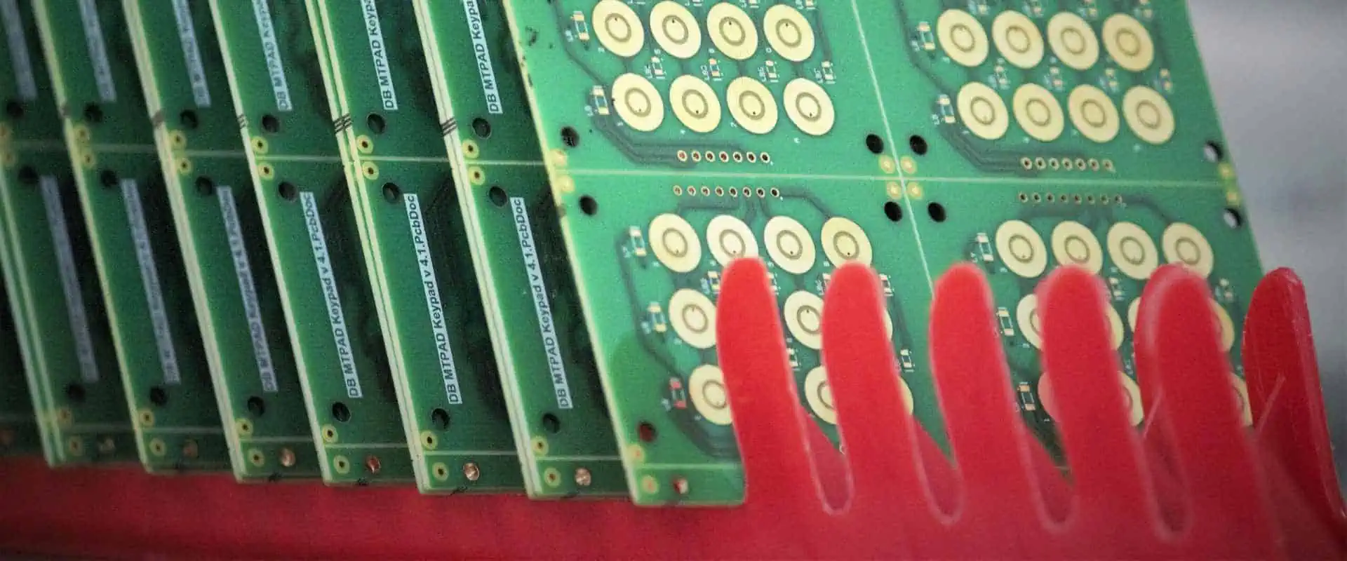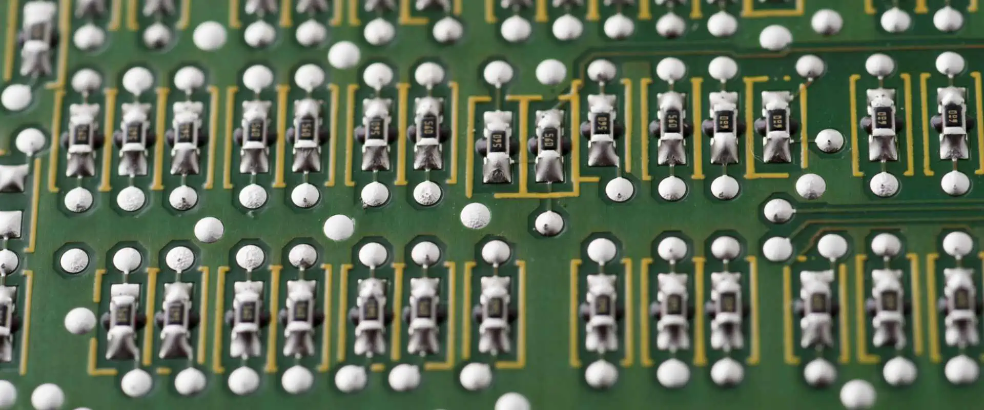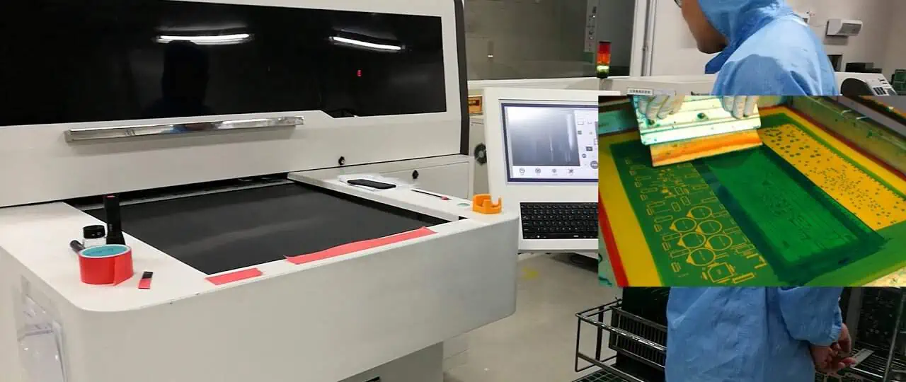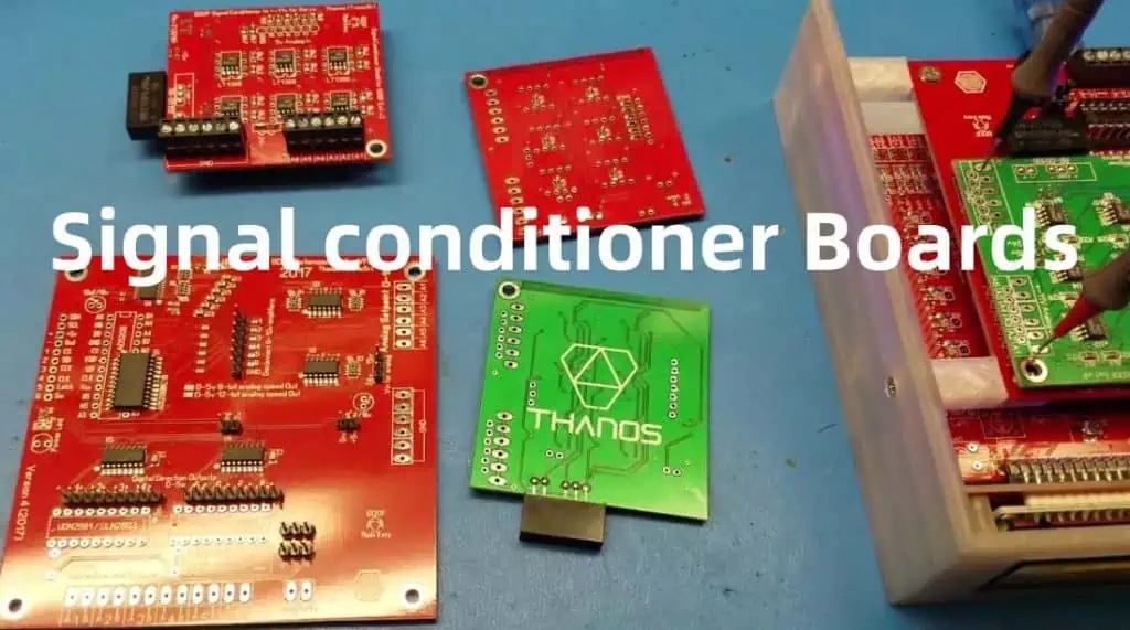
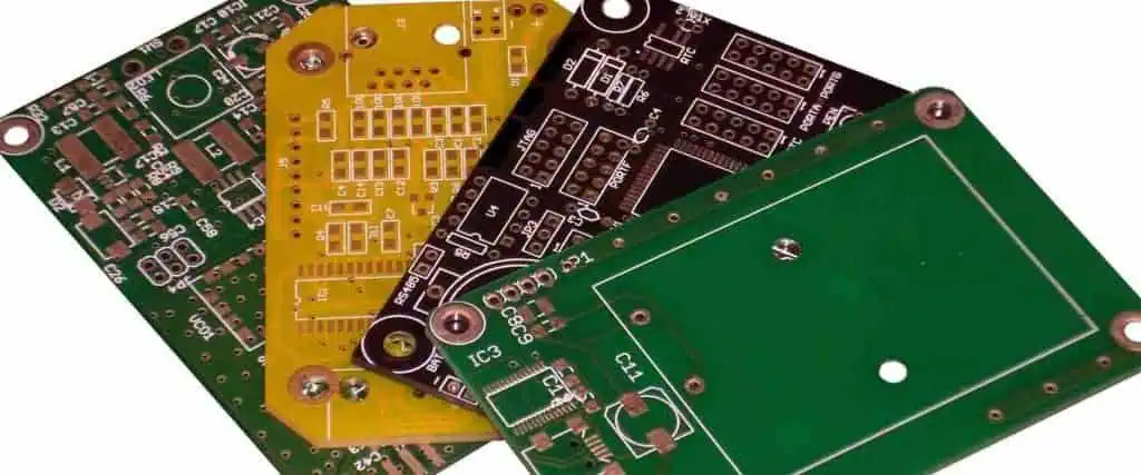
Developing new electronic products requires building multiple iterations of printed circuit board (PCB) prototypes to test and refine the design. Choosing the right PCB prototyping machine is crucial for rapidly fabricating high-quality prototypes at low costs. This guide examines the key types of PCB prototyping machines available and provides guidelines for selecting the best system based on prototyping needs.
Methods of PCB Prototyping
There are several approaches to creating PCB prototypes:
Hand Assembly
- Manual assembly and soldering of components
- Low volumes and iterations
- Flexible but time consuming
- Risk of errors and quality issues
Milling/Routing
- CNC subtractive machining of PCB substrate
- Flexible for design changes
- Limited feature size and complexity
- High equipment cost
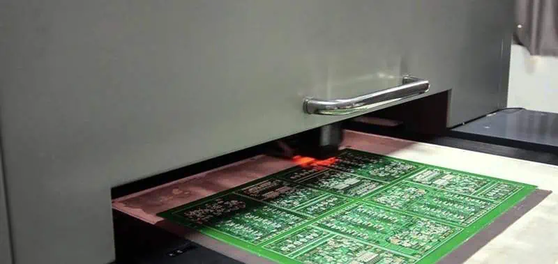
Laser Prototyping
- Laser ablation to selectively remove copper
- Non-contact process preserves fine features
- Limited line width and registration accuracy
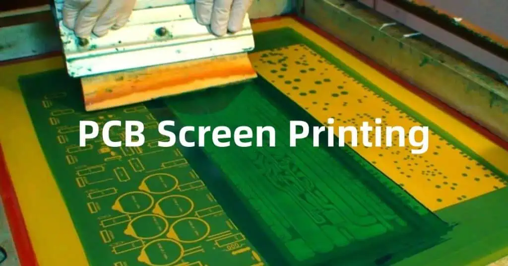
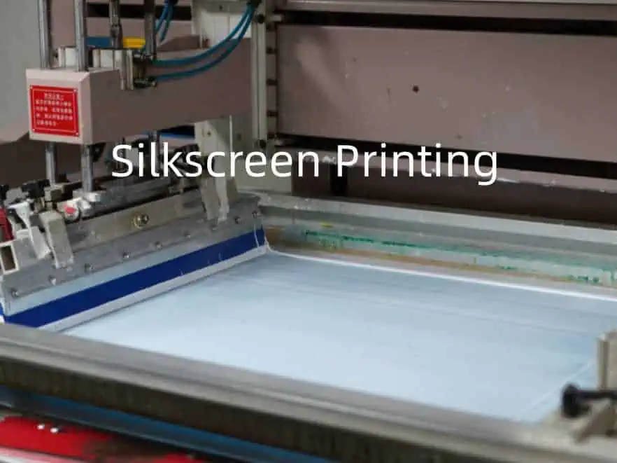
Photochemical Etching
- Uses photoresist and chemical etchant
- Capable of fine features and tolerances
- Multiple fabrication steps involved
- Chemical handling required
Benefits of Automated Prototyping
Automated PCB prototyping machines provide important advantages over manual approaches:
- Speed – Much faster fabrication of multiple boards
- Repeatability – Consistent quality across prototypes
- Precision – Tight tolerances and fine features
- Flexibility – Quick changeover between designs
- Reliability – Reduces human errors and defects
- Scalability – Easily scale to higher or lower volumes
- Productivity – Frees up skilled labor for higher value tasks
For these reasons, using an automated PCB prototyping system is recommended over DIY methods for professional prototyping.
Types of PCB Prototyping Machines
Several types of automated systems have been developed for fast PCB prototyping:
Laser Direct Imaging (LDI)
- Uses laser to image photoresist on blank PCB panel
- Photochemical patterning and etching follows
- Fast imaging with no photo-tools needed
- Limited by etching process throughput
Digital Light Processing (DLP)
- Projector flashes UV light through mask onto PCB
- Photoresist exposure done in minutes
- Still requires wet etching
- Lower cost than laser imaging
CNC Milling/Routing
- Spinning end mill removes unwanted copper
- Drills holes for vias and components
- Flexible but lower precision than etching
- Capable of limited number of layers
Inkjet Printing
- Prints etchant-resistant ink on blank PCB
- Subsequent etching creates conductors
- Additive process builds up traces
- Resolution and accuracy challenges remain
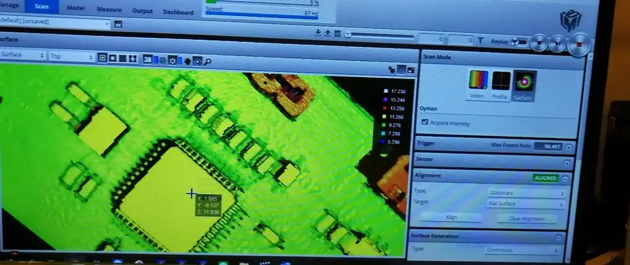
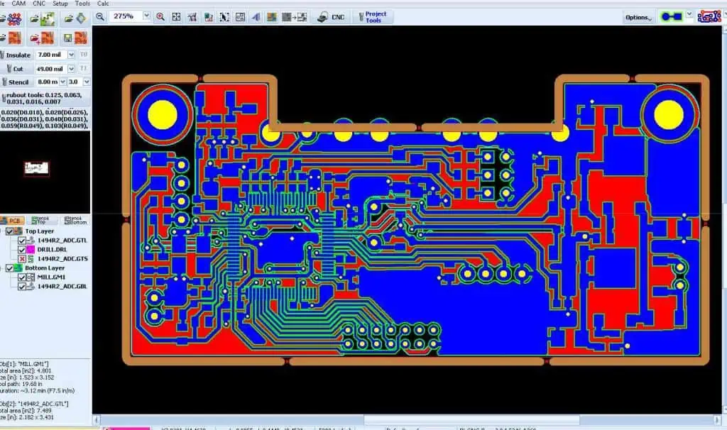
Key Machine Specifications
Important specifications to evaluate when selecting a PCB prototyping system:
- Resolution – The minimum trace/space width that can be produced
- Accuracy – How closely dimensions match design values
- Repeatability – Matching quality across multiple boards
- Throughput – Number of boards produced per hour
- Number of Layers – Supports single, double, or multilayer boards
- Board Size – Maximum dimensions of the PCB panel
- Materials – Compatible board substrates and laminates
- Line Width – Minimum/maximum trace widths supported
- Registration – Alignment accuracy between layers
- Solder Mask – Ability to apply solder resist coatings
- Software – CAM tools for optimizing designs
Laser Direct Imaging Systems
Laser direct imaging (LDI) uses a focused laser to expose photoresist on a copper clad laminate directly based on CAD data. This gives rapid, efficient prototypes without any masks or tooling.
How LDI Works
- Board panel coated with photoresist
- UV laser scans surface, exposing photoresist patterns
- Developer solution removes unexposed resist
- Etchant textures away unwanted copper
- Resist stripped, followed by final finishing
Benefits of LDI:
- Eliminates need for physical masks
- Digital process enables fast changeovers
- High resolution down to 25 microns
- Suitable for circuits down to 0201 components
- Scales efficiently from protoypes to production
Limitations of LDI:
- Wet chemical processing limits speed
- Initial system cost can be high
- Requires skilled operators
- Etching process constrains minimum trace width
Cost Considerations:
- $50,000 to $150,000 for small systems
- $150,000 to $400,000 for production systems
- Lower volumes have higher board costs
- Lower costs at mid to high production volumes
LDI provides the best combination of flexibility, precision and scalability for PCB prototyping.
Digital Light Processing Systems
Digital Light Processing (DLP) uses an LED or arc lamp projected through a photomask to expose photoresist on PCBs with speed and accuracy.
How DLP Works:
- PCB panel coated with photoresist
- Mask with transparent and opaque areas placed over panel
- UV light projected through mask onto panel
- Light hardens resist in exposed areas
- Developer solution removes unexposed resist
- Panel etched and finished as normal
Benefits of DLP:
- Very fast exposure time in minutes
- High resolution with 25 micron geometries
- Small footprint equipment
- Lower cost than laser imaging
- Capable of soldermask coatings
Limitations of DLP:
- Requires physical masks for each design change
- Mask costs and lead time
- Chemical processing creates process bottleneck
- Limited in number of layers
Cost Considerations:
- $30,000 to $100,000 for equipment
- $200 to $1000 for mask tooling per design
- $2,000 to $5,000 per mask set tooling cost
- Lower volumes have proportionally higher costs
DLP provides a lower cost but still flexible PCB prototyping process.
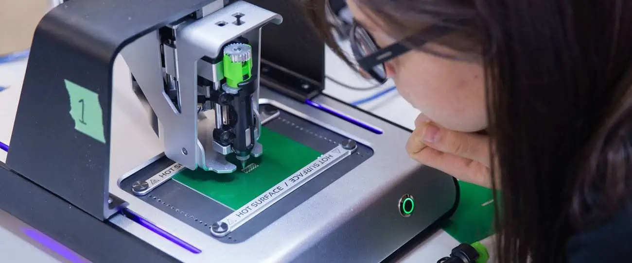
CNC Milling/Routing Systems

CNC milling uses a spinning end mill to selectively remove copper from a PCB substrate to fabricate traces based on CAD designs.
How Milling Works:
- PCB substrate mounted to machine bed
- End mill moves in X-Y over panel removing copper
- Z-axis controls milling depth on panel
- After milling, PCB undergoes finishing
- Components populated on finished board
Benefits of Milling:
- Direct CAD to fabrication workflow
- No chemical processing required
- Capable of quick turnaround
- Design changes easily accomodated
- Allows thick copper PCB substrates
Limitations of Milling:
- Lower precision and tolerances
- Limited to simpler board designs
- High equipment capital costs
- Produces copper dust during milling
- Restricted to fewer layers
Cost Considerations:
- $100,000 to $250,000 for equipment
- $200 to $2,000 per board depending on size
- Economical for very low volume prototyping
- Milling time limits throughput volume
CNC milling suits low complexity PCBs in very small quantities.
Inkjet Printing Systems
Inkjet PCB printing uses inkjet heads to selectively print etchant-resistant ink onto blank copper clad boards. Subsequent etching creates the conductive traces.
How Inkjet Printing Works:
- Blank PCB substrate placed in system
- Inkjet deposits polymeric ink on panel
- Ink hardens to form etchant resist
- Etching textures away unprinted copper
- Resist ink removed and PCB finished
Benefits of Inkjet Printing:
- Direct printing from CAD data
- No tooling or masks needed
- Additive process with no waste
- Small equipment footprint
- Continually improving resolution
Limitations of Inkjet Printing:
- Still lower resolution than etching
- Limited number of conductive ink layers
- Restricted to lower complexity designs
- Conductive ink challenges remain
- Overall process slower than traditional methods
Cost Considerations:
- $50,000 to $150,000 for small systems
- $2,000 to $4,000 per square foot panel
- Only economical at very low volumes
- Cost reduces as technology matures
Inkjet PCB printing is an emerging technology still in development.
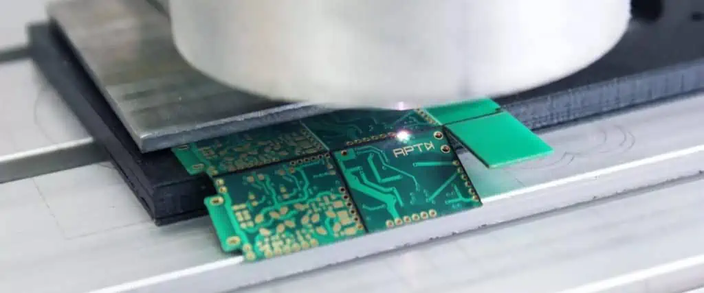
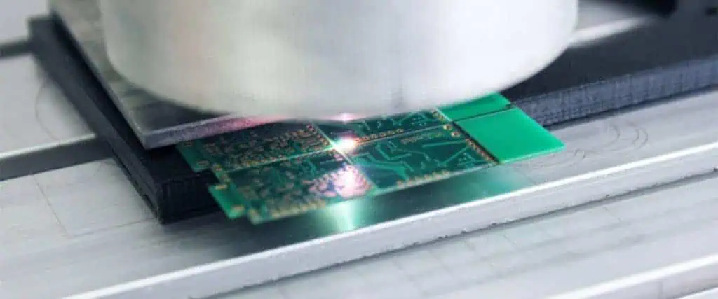
Laser Prototyping Systems
Laser prototyping uses laser ablation to directly remove copper from substrates to form circuit traces based on CAD patterns.
How Laser Prototyping Works:
- Blank copper clad PCB mounted in system
- IR laser selectively ablates unwanted copper
- Desired copper traces remain on PCB panel
- Board undergoes finishing and population
- Very rapid turnaround possible
Benefits of Laser Prototyping:
- No masks, resists or chemistry needed
- Direct non-contact copper patterning
- Extremely fast process speed
- High resolution down to 0.001” lines
Limitations of Laser Prototyping:
- Limited registration accuracy between layers
- Copper smearing and debris issues
- Restricted to simpler board designs
- High equipment cost
- Limited scalability
Cost Considerations:
- $100,000 to $300,000 for equipment
- $500 to $2,000 per board
- Only feasible for very low volume prototyping
- Material costs dominate overall cost
Laser prototyping suits occasional, quick-turn PCB needs.
Hybrid Prototyping Systems
Some systems combine multiple PCB fabrication technologies into a single machine for added flexibility:
Laser Imaging + Etching
- Laser images photoresist like LDI
- Integrated spray etching built into system
- Reduces handling and process steps
Milling + Laser Ablation
- Use milling for bulk copper removal
- Laser ablation gives fine features
- Eliminates masks and chemistry
Inkjet Printing + Etching
- Inkjet deposits etchant resist
- Integrated immersion etching system
- Lower cost digital process
Hybrid machines provide versatility for prototyping needs. But integration complexity can impact costs.
Key PCB Prototyping Machine Criteria
Consider the following aspects when selecting a PCB prototyping system:
- Volumes – Quantity of boards and iterations needed
- Complexity – Simple double-sided or multilayer boards?
- Resolution – Line width and space requirements
- Materials – Substrate types and thickness
- Iteration Speed – How quickly design changes needed
- Technical Expertise – Operator skill level required
- Floor Space – Size limitation for equipment
- Budget – Total investment and per board cost targets
- Scalability – Ability to scale up or down production
Matching the above criteria to the system specifications will identify the optimal PCB prototyping solution.
Making the Right Prototyping Machine Choice
Follow these steps to select the best PCB prototyping equipment:
- Define prototyping requirements – quantity, complexity, precision needed
- Determine suitable technologies – match requirements to process capabilities
- Evaluate vendor systems – compare specifications, features, reviews
- Assess cost considerations – equipment cost, material cost per board
- Validate supplier qualifications – experience, customer support
- Get hands-on demos – test machine usability and output quality
- Consider future applications – scalability from prototyping to production
Selecting the right system will accelerate prototyping, reduce costs, and enhance electronic product development.
Frequently Asked Questions
What are some tips for operating a PCB prototyping machine?
- Ensure proper machine setup, calibration and maintenance
- Follow manufacturer guidelines for photoresist coating, etching, etc.
- Use optimized board layouts and panel utilization
- Allow sufficient tolerances for the process capabilities
- Employ good panel handling practices to avoid damage
How many prototype boards should be fabricated?
Plan for at least 5 copies for design validation builds. Budget needing 10 copies for engineering testing. Produce 20+ copies for field evaluations. Build excess boards to allow for potential failures.
What file formats do PCB prototyping machines accept?
Gerber and Excellon formats are standard inputs. Some systems also accept PDF, DXF, SVG, HPGL, CIF, IPC-D-356A or ODB++ files.
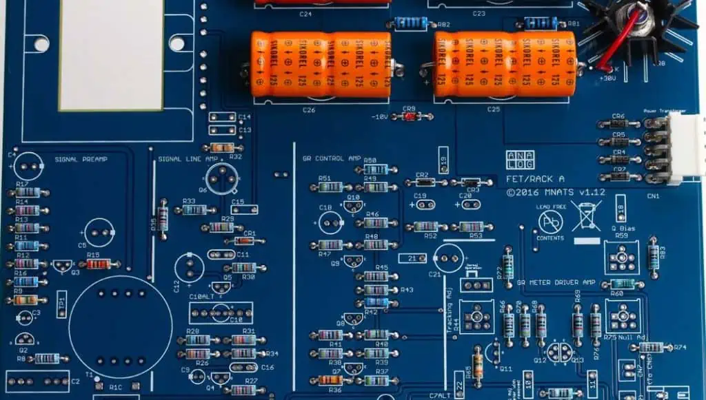
Can PCB assembly be automated after prototyping?
Yes, automated optical inspection, solder paste deposition, component placement and reflow soldering systems enable automated assembly and higher volume production.
How are multilayer PCBs prototyped?
Systems that utilize photolithographic etching can produce multilayer boards through sequential imaging, laminating and drilling of stacked boards. Hybrid milling machines can also create multilayer boards.
Conclusion
Selecting the optimal PCB prototyping system that matches project requirements is key for fast, affordable and effective prototype builds. Laser direct imaging provides the best combination of speed, precision and flexibility for professional needs. But digital light processing, CNC milling, inkjet printing and laser ablation systems have their own advantages that suit certain applications. By analyzing production volumes, design complexity, resolution, accuracy and budget considerations, engineers can determine the ideal system to accelerate innovation and development. Robust PCB prototyping systems empower teams to rapidly test form, fit and function to successfully deliver electronic products to market.