Printed circuit boards (PCBs) are at the heart of electronics. As products become more advanced, PCBs grow more complex. This complexity makes verifying that a PCB matches the original design intent increasingly critical. PCB scans help provide that verification through detailed inspection and analysis.
PCB scans offer a comprehensive way to validate board fabrication quality. This article will explore what PCB scans services encompass including:
- The different types of scans
- Typical scan deliverables
- How scan data gets analyzed
- Use cases showing value of scans
- Options for implementing scanning
- Frequently asked questions
Read on to understand how utilizing scans can improve quality across the PCB development and production cycle.
Types of PCB Scans
There are a few core types of scans used to validate PCB fabrication:
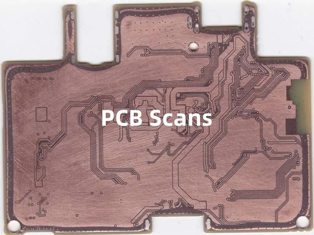
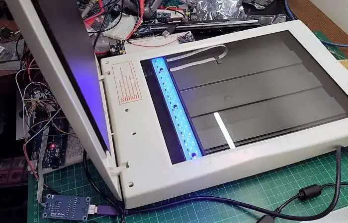
Optical Scans
These use cameras and image processing software to capture highly detailed images of a PCB. The scanned images enable inspection of trace width, spacing, mask alignment, and more. 2D optical scans provide a layer-by-layer view while 3D scans can create models of the entire board.
X-Ray Scans
X-ray scanning reveals internal PCB structure. This allows verification of layer alignment, voids, and defects within the board that are invisible from the outside.
Automated Optical Inspection (AOI)
AOI systems use cameras, lighting, and software algorithms to automatically flag defects on a PCB. This provides fast pass/fail verification to complement manual optical inspection.
Electrical Testing
Testing functionality electrically through in-circuit or flying probe testing. Confirms boards operate as designed rather than just verifying physical traits.
Cross-Sectioning
Physically cutting a sample to expose internals for measurements under a microscope. Most accurate way to assess plating thickness and layer alignment.
These different scans provide complementary views into PCB quality. Optical scans deliver detailed imagery while x-ray and cross-sectioning reveal the board’s internal structure. AOI and electrical testing provide automated defect detection. Typical scan services utilize a combination of these techniques tailored to the specific board and application requirements.
Scan Deliverables
PCB scan services provide a range of detailed deliverables. These help document quality and assist further analysis. Typical deliverables include:
High Resolution Board Images
- Layer-by-layer photos showing fine details
- Captured under precision lighting
- Multiple angles provide complete view
Measurement Annotations
- Board images with measurement callouts
- Critical attributes like trace width documented
- Pass/fail status noted based on specified tolerances
Layer Composite Images
- Overlays images from multiple layers
- Used to assess alignment and stackup
3D Board Models
- Photorealistic 3D model of assembled board
- Enables inspection from any angle
- Zoom into component-level detail
Automated Inspection Data
- Results from AOI inspection
- Log of fails and process metrics
- Used for process control and optimization
Cross-Section Images
- Detailed photos of board cross-section
- Reveals plating quality and thickness
- Assesses inner layer alignment
These deliverables provide full visibility into the as-built state of PCBs. They serve as an important quality benchmark and enable further analysis.
Scan Data Analysis
The scan deliverables provide a wealth of data to analyze fabrication quality. A few examples of how this data gets used:
Dimensional Analysis
The photorealistic board images support precise dimensional measurement of features like trace width and spacing. This verifies all aspects match the original design files.
Layer Alignment Assessment
Layer composites and cross-sections reveal alignment between layers. This includes registration between layers and inner layer skew.
Plating and Etching Analysis
Plating quality and etching characteristics can be inferred from images. For example, uneven plating or over-etching of traces.
Solder Mask Inspection
Mask dimensions relative to copper features are measured. Images reveal solder mask registration errors and insufficient openings.
Voiding and Defect Detection
X-ray scans combined with cross-sectioning uncover voids, gaps, and other defects in the PCB substrate
Process Capability Analysis
Automated inspection data allows statistical process control metrics to be calculated. This reveals fabrication consistency.
These examples demonstrate the breadth of insights possible from scan data. It provides vital feedback for continually improving manufacturing processes.
Use Cases Showing Value of Scans

Now that we’ve explored the scan types and analysis performed, let’s look at a few examples showing the value scans offer across the PCB production cycle:
Research & Development
During R&D, scans help accelerate prototyping by providing detailed validation of new designs and processes. Images allow quick comparison between design and fabricated board.
Pre-Production
Before full production, scans verify that fabrication processes meet specifications consistently across pilot builds. Issues can be corrected earlier.
New Supplier Qualification
When qualifying a new fabrication supplier, scans supply quantitative data about their capabilities relative to requirements.
Batch Quality Monitoring
Periodic scans during production provide ongoing process control. Scan data can detect deviations so corrections can be made before volume production.
Design Issue Diagnosis
If functional issues arise, scans provide detailed physical data to help determine the root cause. For example, whether a short is from a PCB flaw or faulty assembly.
Counterfeit Screening
For products with high counterfeit risk, scans supply physical forensic data to identify boards not produced by approved suppliers.
These examples highlight the benefits of PCB scans during prototyping, ramp-up, and volume production. The data aids issue diagnosis, process control, and quality assurance.
Options for Implementing Scanning

There are a few options available for implementing PCB scan services:
In-House Scanning
Scanning can be brought fully in-house by investing in equipment such as automated inspection, x-ray, and cross-sectioning tools. Offers full control but requires significant capital expenditure.
Outsource to Specialized Provider
Many companies offer outsourced scanning services. These providers supply the equipment, expertise, and capacity needed for on-demand scanning.
Hybrid Approach
Some capabilities like AOI can be brought in-house while specialized techniques like x-ray remain outsourced. This balances control, cost, and flexibility.
Supplier Scanning
Require PCB suppliers to provide scan data as part of fabrication services. Shifts burden to supplier but scan access may be limited.
The right implementation depends on budget, internal expertise, quantity of scans, and quality control approach. As volumes increase, bringing more capabilities in-house makes sense for full control and traceability.
Frequently Asked Questions
A few common questions arise around PCB scan services:
What does PCB scanning typically cost?
Outsourced scan costs range from $250 – $1000 depending on complexity, scan types, and deliverables. Bringing in-house requires equipment investments from tens to hundreds of thousands of dollars.
How long does it take to scan a board?
High resolution optical scans can be completed in under a day excluding time for delivery and analysis. Automated inspection offers even faster turnaround. More complex analysis like cross-sectioning takes longer.
Is scanned data proprietary?
If outsourcing, providers typically retain rights to scan techniques but board data belongs to the customer. Data privacy should be ensured.
What defect detection resolution is possible?
Inspection can reliably detect defects down to 2-5 microns. Smaller defects may be visible but cannot be consistently distinguished from normal variations.
How many boards are needed for sampling?
5-10 samples from a batch provides good insight into quality variation. Complex boards may need more. Both pilot and volume production should be evaluated.
In summary, PCB scans deliver detailed physical validation while questions of cost, time, and implementation depend on specific needs. When used appropriately, scanning adds significant quality assurance value.
Conclusion
PCB scan services provide invaluable verification of board fabrication quality. The variety of scans available equip engineers with multidimensional data to validate PCBs relative to design specifications. Photorealistic imagery combined with automated inspection and cross-section analysis ensure boards meet requirements.
Scans identify issues early when corrections are lower cost. They also provide process feedback to continually refine manufacturing. As PCB technologies advance, scanning offers the level of precision needed to achieve quality and reliability targets. While adding cost, the value realized across prototyping, pre-production, and volume manufacturing outweighs investments. By proactively using scans instead of reacting after functional failures, organizations gain higher PCB quality along with improved time-to-market and lower risk.