What are the Various Electronics Manufacturing Standards?

ย Electronic Circuits

If you notice, the color of most printed circuit boards is green. The unfortunate fact is that nothing is green about them. The truth is that, waste from PCB generated decades back will keep harming our environment for years. This pcb waste, which is made of hazardous substances that includes heavy metals like mercury, lead, cadmium and many other chemicals that affects human health and life adversely.

This is why environmental manufacturing is necessary for RoHS compliant PCB assemblies across all consumer electronics. RoHS (Restriction of Hazardous substances) helps in restricting manufacturers from making use of any hazardous material, most especially those found on electronic and electrical components.

Furthermore, in 2002, the European Union instigated this RoHS directive, which is under the directive 2002/95/EC. Regarding the initial directive, there are six substances that are hazardous and have been prohibited from use in packaging electronic circuits and electrical products.

As of today, the RoHS directive has seen two upgrades, which includes the RoHS 3 and RoHS 2. The release of the latter, which is also Directive 2011/65 /EU, was back in 2011. That of Directive (EU) 2015/863 was released back in 2015. Also, under this new directive (EU) 2015/863, there were four more elements added to the initial restricted elements.

What Does it Mean to be RoHS Compliant?

The parliament of the European Union back on 27th Jan 2003 passed two laws or legislations, which had an impact on the electronics industry. First, was the WEEE (Waste Electrical and Electronic Equipment), which makes the manufacturers responsible for disposing of waste of finished goods. Furthermore, the second legislation is much more important. This refers to RoHS (Restriction of Hazardous substances).

With this RoHS directive, it is illegal if you manufacture electronic or electrical equipment containing restricted materials, as well as materials that can harm the environment. This legislation took effect on 1st July, 2006. Also, the focus of this directive is on the smallest possible RoHS material or homogeneous part, which you can separate from an assembly or component mass.

Specifically, the electronic or electrical equipment that enters the European Union market cannot have cadmium, mercury, lead, polybrominated diphenyl ethers, specifically Octa PBDE and Penta PBDE or polybrominated biphenyls, and hexavalent chromium.

Materials that are Restricted Under the RoHS Compliance

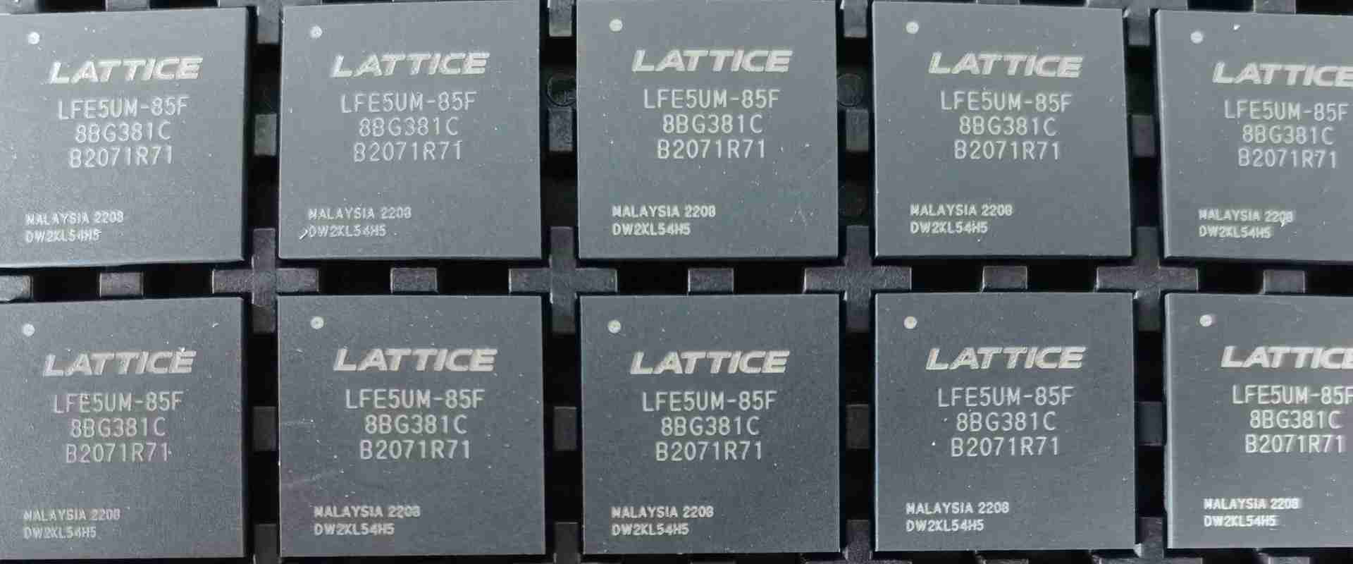
Six major materials cannot be used in PCB due to the restriction caused by RoHS compliance. These include Lead, Mercury, polybrominated biphenyls, Hexavalent Chromium, polybrominated diphenyl ethers, and phthalates like DIBP, BBP, DEHP, and BBP.

This compliance specifies the highest levels these materials can be in a PCB as well as other electronics.

  • Mercury < 100 ppm
  • Cadmium <100 ppm
  • Lead <1000 ppm
  • Hexavalent Chromium <1000 ppm
  • Polybrominated Biphenyls <1000 ppm
  • Polybrominated Diphenyl Ethers <1000 ppm
  • Benzyl butyl phthalate <1000 ppm
  • Diisobutyl phthalate <1000 ppm
  • Dibutyl phthalate <1000 ppm
  • Bis (2-Ethylhexyl) phthalate <1000 ppm

What are the Impacts of RoHS Compliant PCBs?

As of 1st July 2006, the new electronic and electrical equipment hoping to enter the SU market, must not have cadmium, mercury, lead, polybrominated diphenyl ethers specifically Octa PBDE and Penta PBDE or polybrominated biphenyls, and hexavalent chromium. Below are other impacts of ROHS compliant PCBs.

Lead-free manufacturing

Though there is no restriction in the use of flame retardants in laminates, this lead-free initiative will also affect the supply chain. This means that manufacturers of lead free PCBs will not be able to make use of RoHS compliant surface finishes. Also, during assembly, lead solder must not be used.

For this reason, lead-free soldering will need a higher temperature before it can solder, while the raw PCB must have the ability to withstand higher temperature. Furthermore, new laminates will require better thermal and mechanical properties to be able to withstand any lead-free manufacturing, with respect to long-term stability and infant mortality.

Material restriction with respect to RoHS directives

The ROHS 3 directive bans the use of some hazardous elements, about ten in number. This is useful in electrical and dedicated service electronic products as well as high performance electronic products. In addition, the chemicals and substances used during PCB assembly and PCB manufacturing must not have these elements even in impurity form.

The quantity permitted in impurity form is determined in the RoHS directives. Take for example, the amount of cadmium you can have is restricted to 0.01% in impurity form.

Implementation Cost

When considering the protection of the environment, as well as our future as humans, cost isnโ€™t a problem. However, we should understand what is involved when implementing RoHS. All lead-free solder will cost a minimum of 20% more compared to lead soldering.

Donโ€™t focus on the cost of the material alone, there will also be an increase in energy cost. Regarding lead-free soldering, there is a need for higher temperatures for reflow soldering. As regards the cost for training the personnel to handle the lead-free environment change, there is a huge cost as well.

Some lead-free materials will include patent licensing costs, whether by the solder manufacturer or end-user. Also, there is a high cost to refine lead-free materials like gallium, indium, bismuth, and silver.

Reliability Concerns

The change of solder and materials so as to accommodate lead removal needs reliability testing. Techniques, models, and criteria for reliability testing must be refined so as to match the properties of lead-free assemblies. Below are some other concerns

Tin whiskers

Whiskers could result in short PCBs. This problem could become very serious because a good number of component manufacturers make use of pure tin as their lead finish to help in minimizing costs.

Solder joint reliability

The reliability of lead-free joints is less in contrast to lead soldering. Majority of researchers have discovered the long-term reliability of the solder joint is less compared to the lead/tin solder paste.

Higher-temperature soldering

An increase in soldering temperature will lead to a reduction in the componentsโ€™ life, multilayer PCB delamination, thermal fatigue, etc.

RoHS standard (IPC-A-610)

This is electronic assembliesโ€™ acceptability. This standard comes with approved and industry-developed programs such as instructional material, certification, and training. Companies providing RoHS compliant PCBs should have IPC trained workmen to offer the right attention to the necessary changes, as well as renewed criteria for inspection.

Solder Flux

The fact is some solder flux utilized for tin or lead cannot resist high temperatures. For this scenario, if we are making use of that same flux utilized for the lead, then it must evaporate, oxide, or decompose before the fluxing can happen. Therefore, this lead-free solder flux has to be designed in order to withstand any higher temperature.

Why is RoHS Compliant PCB Necessary?

The major concern starts with the electronic waste piles which are usually seen in junk yards that are open across the globe. This electronic waste is usually made of hazardous substances like heavy metals, as well as other chemical materials having no chemical control.

This problem further persists as this acidic rainwater will dissolve the lead as well as other negative and harmful substances. The contaminated rainwater is then added to the bodies of water. Therefore, this can cause severe harm to humans and aquatic life.

Also, heavy metals such as mercury and lead affect the human organs adversely. This could even disturb the whole central nervous system. Also, the metals affect how the reproductive system and the kidneys function. Taking high amounts of lead through a contaminated water source will surely reduce the time of reaction to the body organs like ankles, wrists, and fingers.

With the RoHS initiative, we all get some relief. Complying with the RoHS directives will ensure the fight against global warming and climate change.

RoHS Compliant Printed Circuit Boards

RoHS Compliant Printed Circuit Boards lack hazardous substances and chemicals. Also, RoHS compliant printed circuit boards are now in high demand as a result of the increasing preference towards circuit boards that are environmentally friendly.

This rise in demand for manufacturers adhering to RoHS compliance requirements for their printed circuit boards is as a result of the strict government policies and customer demands. We are beginning to witness a shift with respect to environmentally-responsible manufacturing all through the globe. In addition, RoHS compliant manufacturing helps in reducing the ill-effects that could come to workers when manufacturing is on.

What are IPC Standards?

These IPC standards are different from the RoHS standards. IPC is an association that produces standards related to printed circuit boards. This association was initially referred to as the Institute for Printed Circuits and this is where the IPC acronym came from. Even though it retained this acronym, it is now called Association Connecting Electronics Industries.

IPC is an association for the international industry that consists of over 4000 companies that makes, uses, specifies, and designs printed circuit boards (PCBs) and other assemblies including:

Furthermore, these IPC standards are standards adopted in the electronics industry for electronic assembly, PCB manufacturing, and design. For all steps of the design, the production, and the assembly or printed circuit boards, there is always an IPC standard.

Conclusion

Here comes the end of our article on the different standards used in the electronics manufacturing industry. Any questions, please ask us immediately.

Review of Lattice LFE5UM-85F-8BG381C Programmable Logic IC

Lattice LFE5UM-85F-8BG381C

Lattice LFE5UM-85F-8BG381C is one of the Programmable Logic Integrated Circuits (ICs) designed by Lattice Semiconductor Corporation. Generally, Programmable Logic ICs are mini or small electronic components solely used for the building of reconfigurable digital circuits.

Programmable logic ICs are sometimes referred to as Programmable Logic Devices (PLDs).

Background Information on Lattice LFE5UM-85F-8BG381C

Lattice LFE5UM-85F-8BG381C is manufactured by Lattice Semiconductor Corporation. It is one of the Programmable Logic ICs under the LFE5UM family series.

With its embeddable design, the IC can be added or integrated to circuit boards for reconfiguration and reprogramming purposes.

Technical Specifications of Lattice LFE5UM-85F-8BG381C

Below is a table representing the technical properties and attributes that make up the Lattice LFE5UM-85F-8BG381C Programmable Logic IC.

Technical AttributesDescription
Mounting StyleSurface Mount Technology (SMT)
Operating Temperature (min-max)0หšC ~ + 85หšC
Moisture SensitivityYes
Voltage Supply (min-max)1.04 volts to 1.155 volts
Number of Inputs and Outputs (I/Os)205
Number of CLBs/LABs21,000
Number of Logic Cells/Elements84,000
Operating Voltage Supply1.11 volts
Total Number of RAM Bits3833856
Product StatusActive

How Lattice LFE5UM-85F-8BG381Cโ€™s Programmable Logic IC Works

We are now going to talk about the Programmable Logic Integrated Circuit (IC) of the Lattice LFE5UM-85F-8BG381C FPGA.

As mentioned earlier, a Programmable Logic IC is a small electronic component, which is used to facilitate the reconfiguration of digital circuits, such as Printed Circuit Boards (PCBs).

Advantages of the Lattice LFE5UM-85F-8BG381C Programmable Logic IC

In this section, we are going to help you understand the benefit of buying the Lattice LFE5UM-85F-8BG381C. Here are some of the advantages that come with a Programmable Logic IC:

1. Compact Size

This is perhaps one of the features that digital designers look for, because the circuit board needs to have enough space.

Through the interconnection of the components, Lattice LFE5UM-85F-8BG381C Programmable Logic IC can save space.

2. Flexible Configuration

Configuring or reconfiguring/reprogramming the circuit board is simpler, thanks to the inclusion of necessary architecture.

For example, the design change can be done in a jiffy, as well as the modification of the circuit boardโ€™s overall design.

3. Less Power

The IC doesnโ€™t use up all the power/current in the board, so that it is a great way to conserve power when working on a digital circuit board project.

4. Laid-Out Configurability

The overall configuration of the Lattice LFE5UM-85F-8BG381C is simplified, with the use of:

  • Quick adoption and or integration of new technology.
  • Easy troubleshooting
  • It is easy to check the designs.
  • Simplified design process, especially when compared to random logic gate networks.

Downsides to Using the Lattice LFE5UM-85F-8BG381C Programmable Logic IC for Your Designs

Although has a lot of unique upsides, it also has some downsides. Here are some of the advantages of investing in the Lattice LFE5UM-85F-8BG381C Programmable Logic IC:

1. Flexibility isnโ€™t All-Round

Lattice LFE5UM-85F-8BG381C isnโ€™t all-around flexible. For example, the integration of certain external components, such as an analog box isnโ€™t easy to do.

2. Custom Production

Some components are subject to custom design. An example is the connection mask.


Conclusion

Lattice LFE5UM-85F-8BG381C Programmable Logic IC is a device that can simplify how you configure your Printed Circuit Boards (PCBs). Its reconfiguration capabilities enable faster changes and modifications when they are needed.

Contact RayPCB for professional guidance on how to maximize the IC to its fullest.

Why a PCB Ground Plane is Crucial for PCB Functioning

PCB Ground Plane

Electronic devices depend on a firm foundation for operation. This foundation is usually found in a printed circuit board. The ground plane which comprises a layer of metal is the foundation of PCB. A PCB ground plane is critical for PCB design and manufacturing. A good foundation depicts great functionality.

Grounding is crucial for any electronic circuit that deals with electric current. Printed circuit boards are crucial to the functioning of almost all electronics. Therefore, each circuit board requires a proper ground plane for proper functioning.

What is a PCB Ground Plane?

A PCB ground plane comprises metal layers within the stackup of a circuit. Also, it is a large area of metal directly connected to the circuit ground. These layers take a small portion of the PCB. However, they may take an entire board layer in a multilayer PCB design. Also, they take up multiple layers based on the requirements of the design.

The PCB ground plane occupies a vast area that is associated with the energy supply potential. Ground plane offers several functions. Also, they help in voltage return. Almost all components on the circuit board will link to a power net. The return voltage will return via the ground net. Also, wider traces help to route ground nets when PCBs have one or two layers.

According to the PCB models, it is possible to alter the PCB ground plane. For instance, the bottom layer is mostly used for the ground plane in a two-layer PCB. However in a multi-layer PCB, designers use the entire layer for grounding. Also, this helps to prevent issues like signal traces and ground loops.

It is crucial to determine the appropriate PCB ground plane technique to use to achieve the best result. Otherwise, unnecessary problems may arise. For instance, an inappropriate ground plane can result in signal crossroads and EMI. Also, electromagnetic interference can result from other components on the PCB. PCB ground planes are that large portion on a PCB that comprises metal layers. However, they could occupy a small portion of a board.

What is the Function of a PCB Ground Plane?

PCB manufacturers connect ground planes to the circuit ground of the PCB. Also, the requirements of the PCB layout determine the area of a ground plane. Therefore, a PCB ground plane can be a small part of an entire PCB. Sometimes, it could occupy a vast area of the PCB. So, what functions does PCB ground plane perform in printed circuit boards?

Signal recovery

When two tracks are parallel to each other, one of the tracks may engage with the other through electromagnetic induction. In this case, a PCB ground plane plays a crucial role. Also, a good ground plane ensures signals return without disrupting other parts of the PCB. Without a clear path for signals to return, there can be a lot of interference for the PCB.

Minimizes noise and interference

A huge amount of energy discharges through the ground circuit anytime there is a shift in the digital circuitsโ€™ position. Therefore, this action generates several noise and interference. Also, you can avoid these issues by integrating ground planes.

Voltage recovery

 A PCB comprises several elements inside. Over 90% of these elements connect with a power net while in use. Furthermore, the voltage appears through the ground net. The designer must use wider tracks if there are PCBs with less than four layers. Also, circuit boards with many layers need special attention. In such a case, the manufacturer has to use a good sheet of ground plane. Therefore, this will help to achieve a good connection between the ground nets and the elements.

Power integrity

PCBs often comprise electronic components that require a lot of power during operation. Therefore, PCB ground planes smooth out the power spikes created by this operation.

Design Guidelines for PCB Ground Planes and their Connections

You can use PCB design tools to create a plane. However, layout recommendations are crucial when working with ground planes in PCB design. Also, they help to design the most effective ground system possible.

Multilayer designs

Multilayer designs need layer stackups with the right configuration of layer widths and ground layers for proper routing. Also, designers can effectively create a PCB ground plane in the CAD system as negative or positive images. In several instances, you will need additional area fills of ground for the entire design.

Routing

You need to route the ground using the widest trace for a single layer board. However, it is advisable to design a PCB ground plane to leverage some electrical benefits.

Connections

Ensure traces from SMT pads to via grounds are wider enough to lower their inductance. However, avoid using too wide traces on small discrete parts.

What is an Antenna Ground Plane?

The antenna ground plane serves as a simulated ground. A antenna requires a metal surface to launch signal into the atmosphere. For a monopole antenna, the antenna ground plane reflects the radio waves so that the Earth sees the image of the top half of the antenna. Also, you can use a conducting plane to replace the real earth. To function as a ground plane antenna, the conducting surface must extend from the base of the antenna.  

It isnโ€™t necessary to offer a full circular conducting plate for a ground plane. This is because it would be very difficult to manage. Also, it is better to have a ground plane that comprises a number of quarter wavelength radials. Most times, there are four conducting radials. These four radials offer enough simulation of the entire circular ground plane.

A ground plane antenna is different from an electrical ground. Also, a ground plane antenna is mainly designed to function on fiberglass boats and vehicles.  

Conclusion

A PCB ground plane is important in PCB design and manufacturing. Also, designers use a power or ground plane in multilayer stackups. A good ground connection is necessary for great performance in a printed circuit board. A ground plane prevents electromagnetic interference in PCBs. Designing a circuit board requires an effective ground plane. Here, we have discussed how to achieve good grounding for your boards.

How First Piece Inspection Procedure Enhances Production Quality

First Piece Inspection Procedure

Certain documentations are crucial in a production process. The first piece inspection details a procedure for evaluating, dispositioning, and delivering first piece samples. In this article, we will shed more light on the first article inspection.

What is First Article Inspection?

First article inspection (FIA) involves planning, manufacturing, and confirming a production process. Also this process determines if the production process for a part can consistently supply parts that conform to specifications. Also, a first article reviews the entire manufacturing process. It looks at how raw materials go through the production process. This includes functional testing for a part.

A first article inspection (FIA) is crucial for both producers and buyers of a part. It helps the manufacturer to evaluate the manufacturability of a part and identify design errors. Also, FAI helps buyers to verify that the manufacturer understands the design requirement.

The buyer will be able to assess the manufacturing process and external special procession steps.

When do you need a First Article Inspection?

FAI is critical during a new product manufacturing process. Also, it helps to ensure if the manufacturing process can deliver products that comply with specifications. A first article inspection requirement need to assess one part with the unwritten assumption every part will follow the same production process.

Any alteration in the design or manufacturing process of the part violates this assumption. Therefore, there is a need for a first article inspection. Below is the list of conditions that needs a new first article:

  • A factory move
  • Manufacturing process change
  • New product introduction
  • Design change

You will need a new FAI for some changes. For instance, you will need a new FAI for any change from laser cutting to stamping. Also, a change to how parts are packages may not need a new first article inspection.  FAI is an inspection equipment that helps to achieve a quality management system.

What is First Article Inspection Report?

 A first article inspection report (FAIR) is a document that approves that every sample was manufactured and inspected based on the specifications of a customer.  Also, the first article inspection report is widely used in the aerospace industry. This report is in three different forms which are form 1, form 2, and form 3. Also, the three forms offer a full record of the production process.

Form 1 (Part number accountability)

Form 1 refers to the Part Number Accountability. Also, this form achieves three main objectives which are:

  • Ensuring traceability to the production process
  • Confirming traceability to the engineering change order
  • Linking the parent FAI to the report for every sub-component utilized

Form 2 (Product accountability)

There are two subsections in form 2. Also, these include raw materials and special processing section and a functional testing section. For instance, raw materials may comprise a block of AI6061 T6, a copper tube and a conductive epoxy.

Form 3 (Characteristics Accountability)

This is the characteristic accountability form. Also, you may define a part by hundreds of material and functional parameters. Form 3 lists and accounts for every parameter. Also, you will need to provide the balloon number or characteristics for every parameter. Note, you must provide the drawing sheet and a characteristic designator for every parameter.

How to Create a First Article Inspection Report

There are steps involved in creating a first article inspection report (FAIR).

Pre-plan your FAI

Before starting, you need to get the documentation required for your First Article Inspection (FAI). This includes:

  • Specifications
  • Supplier/source data
  • Raw materials list
  • Engineering drawings
  • Digital product definition data sets
  • Manufacturing plans

Design an inspection plan

You will need to balloon your part drawing. This involves identifying the requirement you need to inspect with a balloon number. Also, get the AS9102 forms ready for the inspection.  You will need to fill the AS9102 form 1 and Form 2 with the details from the Specifications List and Bill of Materials. Also, you will need to fill out the AS9102 Form 3 with inspection tools, dimensions, and tolerances notes. You will need the serial number and type of tool.

Produce the part

Create the product and document the processing and inspection results for the requirements during the production process.

Collect data

You will need to inspect the part. Also, keep track of approved inspection tools. This will help you trace them back to the person approved to utilize the tool to inspect or manufacture accurately.

Create the report

Fill the measurement result data in the AS9102 form 3. Also, these include Certificate of Conformance and Functional Test Report.

PPAP and FAI: What is the Difference?

FAI is a part of the production part approval process (PPAP). Therefore, there are some crucial differences:

First article inspection (FAI) only demands for the inspection of one part. PPAP demands for the production of many parts for run-at-rate and process capability. Also, a PPAP needs formal documentation for each step of the new product introduction process. On the other hand, first article inspections mainly concentrate on the subset of the documentation like raw materials, processing, and functional testing.

Companies that choose the First Article process often believe that there are some Quality Control Plans already in place. Also, the production part approval process and FAI are both important in manufacturing.

What is First Article Manufacturing?

First article manufacturing involves manufacturing the first unit o a product. This sample unit provides customers the assurance of seeing their case in a format. Also, first article manufacturing is beneficial when it comes to product evaluation.

Before a huge production run, this process offers customers the chance to verify if their custom case matches with the dimension and designs.The custom case must match with the designs and dimensions outlined in certain specifications. Also, first article helps customers to verify if the cases perform as expected. Furthermore, they can verify the durability and quality of the solution.

A large volume production run can take place after this. Also, the first production run can commence after verification has occurred.  

Conclusion

The first article inspections play a crucial role during a production process. Also, the FAI process comprises several steps. Most companies integrate this document to enhance their quality system and production tools. Also, the first article report is very important.

CSP BGA: What are the Differences Between CSP Package and BGA Package

eMMC BGA

There has been some confusion regarding the differences between the CSP and BGA packages. Due to constant requests, we have decided to do more research and come up with an article that answers your questions.

In this article, we will be explaining from a neutral point what CSP and BGA packaging is. Furthermore, we will go on to explain the differences between the two, with respect to their features. If you need to widen your knowledge on this topic, get ready as we explain further.

What is CSP and BGA Packaging?

For some years now, many people understood the need to underfill flip chip devices. The traditional large BGA (ball grid array devices) are underfilled only on very rare occasions, probably when that specific device will be useful in some critical applications like flight computers. For some years now, there has been a debate regarding the importance of underfilling CSPs (chip scale packages).

Majority of package manufacturers try designing CSPs to prevent the underfill requirement. However, practically, the underfill CSP (chip scale package) will have a higher reliability in contrast to one not underfilled. Majority of manufacturers usually underfill the CSPs whenever the parts are utilized in applications for portable electronics which users usually drop.

Whenever the testing of the product reveals that there is a need to underfill a device, the next step you should take is determining the best underfill process. In this article, we will be discussing the differences when it comes to flip chip, the BGA and CSP device reviews and underfills where and when to make use of each process. Let’s continue as we do some csp bga comparison

Differences Between CSP Package and BGA Package

CSP BGA

For newbies who have taken a BGA rework, so many people out there do not know the best way of distinguishing the CSP packages (chip scale packaging) from the BGA packages. Here we will clearly differentiate the difference between the two.

Ball Grid Array (BGA) Package

Due to the development of integrated circuit technology, the requirements for packaging integrated circuits are now more stringent. Why is this so? This is due to the relationship between the packaging technology and the productโ€™s functionality. Whenever the ICโ€™s frequency surpasses 100MHz, this traditional method for packaging may produce what is called the โ€œCrossTalkโ€ phenomenon.

Whenever the pin number is more than 208, this traditional method for packaging is difficult. Therefore, aside from the QFP method of packaging, the majority of high-pin count chips (like chip sets and graphics chips) are now making use of the BGA packaging technology.

Furthermore, for packages like CPUs, BGA has now become the most acceptable choice. For sure, there is a concern for many people regarding the BGA rework packages.

Categories of BGA Packaging Technology

Plastic BGA (PBGA)

This is a multi-layer board, which is made up of two to four layers of different materials. Note that, among the Intel series central processing units, the Pentium IV, III, and II processors make use of this package.

CeramicBGA Substrate (CBGA): The electrical connection, which is found in-between the ceramic substrate and the chop is mounted via the Flip Chip (FC). Note that, among the Intel series central processing units, the Pentium Pro, Pentium II, and I processors make use of this package.

Flip Chip BGA (FCBGA): This is a multilayer and rigid substrate

Tape BGA substrate (TBGA): This substrate refers to a soft strip-shaped PCB circuit board of 1-2 layers

Carity Down PBGA (CDPBGA): This substrate has to do with the bare chip area, which is also referred to as the cavity area having a low depression at the packageโ€™s center.

What are the Features of the BGA Package?

  • Though there is an increase in the input output pins, there is a much larger distance in-between the pins compared to the QFP packing that aids yield improvement.
  • Though there is an increase in BGA consumption, since controllable chip welding is usually used, there can be an improvement in electrothermal performance and thermal expansion.
  • There is a small delay in signal transmission, while there is great improvement in adaptive frequency.
  • You can make use of co-planar welding for assembly. This helps in improving the reliability greatly

CSP Package (Chip Size)

With the increase in demand for lightweight and personalized electronic products globally, their packaging technology has seen great advancements to the Chip Size Package (CSP). This reduces the chipโ€™s package size, making sure that the IC has over 1.2 times of the chipโ€™s side length, and the area of the integrated circuit (IC) is a maximum of 1.4 times larger compared to the die.

All You Should Know About Manufacturing Electronics in China

EMS Electronics Manufacturing Companies

China’s wholesale electronic suppliers have contributed greatly to our global economy. Its deliberate focus is on the improvement of the product’s quality assurance and not the quantity.

In 2019, the technology wholesale market of China reached an ATH (all time high) with more than $20,747.10 million in exports. In years to come, it is expected to increase even further.

You will no longer feel disappointed. However, you will feel empowered whenever you see the label “made in china” on any digital gadget.

Where are the Main Provinces in China for Manufacturing Electronic Products?

Global companies usually look up to China for electrical and digital product manufacturing in Guangdong, Shanghai, Zhejiang, Shandong, and Jiangsu. Currently, these cities are known to house about 33% of the industrial output of China. Coincidentally, these provinces are also responsible for most of the merchandise exports of China.

Zhejiang and Shanghai are situated in the southern area of the River Delta. Majority of foreign companies situated their China manufacturing activities in Suzhou, which is also a part of the region. In addition, Nanking is another center of the electronics industry, which is a bit farther inland from the Yangtze river.

Located in the south is Shenzhen, another huge manufacturing hub that is located in China. This is the largest manufacturing center for all consumer electronics in the country. These include well-known devices like smartphones and tablets. Majority of China’s top tech companies are located here.

Zhongguancun, also the Silicon Valley of China, houses a large number of non-Chinese technological companies. The headquarters of Microsoft and Google is here, as well as their research centers.

Lastly, Shenyang is a home to lots of software developers.

Current Trends in the Manufacturing of Electronics

The consolidation of electronic components manufacturing, and finished devices, coupled with the logistics associated with getting the items in the hands of consumers and customers are the present trends that drive Chinaโ€™s manufacturing world.

Strategic partnerships assist companies in offering a very wide range of services. Also, they make many choices available to their customers just from one source.

Customers are now seeing this as beneficial when purchasing electronic components and electronic devices. Also, attention spans now get shorter and there is this mentality of wanting things done immediately.

Furthermore, the internet provides a great selection of products by just clicking a button. There is also an expedited shipping option. The trends are spilled into the customer also.

The โ€œwanting something done immediatelyโ€ mentality has made effective logistics a factor for businesses and consumers alike. Now, rapid delivery is now very important.

Best Electronics Manufacturers and Wholesalers in China

rayming hdi pcb

Below are some companies and contract manufacturer involved in wholesale supply of electronics and electronics manufacturing in China at a very low price.

Shenzhen Hosing Technology

This high tech company is majorly focused in manufacturing USB cables, power banks, phone and car chargers, etc. A power bank serves as a portable charger for cameras, worldโ€™s mobile phones, as well as other digital electronics.

Furthermore, they provide wide flexibility when it comes to product design, compatibility, capacity, specifications, as well as smart safety features. Also, they function under the ISO 9001, which is a system of quality management recognized internationally regarding design and global production base. They have a market in North America, Middle East, Europe, and many other places globally.

Contact this company here

Guangzhou YOUTOP Technologies

This company is focused on the development, design, and manufacturing digital gifts (custom-made) for promotional purposes.

Founded in 2004, the company works closely with it’s customers to get the perfect product for you. Furthermore, their employees possess great understanding of research and development. Also, they strive to deliver recent technologies.

Globally, they have also teamed up with some well-known enterprises and their products are popular across the global markets. Also, their products work with the health regulations of today, including C3, CE, and RoHS.

Contact this company here

Shenzhen Linbova Technology

This is a smaller company, which focuses on producing Bluetooth speakers, outdoor electronics and game controllers. It was established back in 2017, and it is highly competitive, as it implements engineers involved in research and development, who can customize their products so as to meet your needs.

In addition, this company operates under the management certificate of ISO 9001. Also, their process of production is properly overseen by the skilled technicians and engineers.

Please contact this company here

Huaqiang Electronic World

In China, this company is widely known to own one of the largest internal and external markets for consumer electronics. Its six floors showcase virtually all types of electronic gadgets present. Hardly will a customer get here and not find what he or she wants.

Also, they have some innovative and sustainable technology such as lamps and chairs entirely from recycled cardboards.

You can contact Huaqiang Electronic world here

B&K Electronic Technology

This is a trading company which was founded in 2017. This period it was new to a very competitive market and its operations were conducted by just 9 employees.

They are involved in the Chinese manufacturing project of electronic gadgets like wireless phone chargers, different phone cases, and bluetooth headphones. Each employee here has at least a 10 year background or experience in business and they have assisted top tech companies to bring their different products to the market like Apple, Huawei, and Samsung.

Contact this company here

Marvel Electronics

This electronics manufacturing company was established back in 2012. Specifically, it deals with the manufacturing of LCD modules like animated graphics, TFT LCBs, dot-matrix, and alphanumeric. Also, they manufacture things such as optical cables, computer speakers, custom designed flash drives, tablets, androids, phones, flash drives, and more.

Marvel Electronics offers highly competitive prices. It also offers its services in different continents including North America, Africa, Middle East, Australia, and Europe.

Contact this company here

Flying Communication Limited

This company was founded back in 2004 and is well-known to produce different phone cases, like athletic ones, earphone cases, hybrid cases, waterproof cases, as well as screen protectors.

On average, their annual sales stand between $200 and $500 million. They may not be involved in producing electronic gadgets, but they are well-known for phone cases for about 14 years now.

Contact this company here

Conclusion

Here comes the end of this article. Feel free to contact us if you have any questions.

The Features, Applications, and Benefits of Invar Controlled Expansion Alloy-Foil PCB Materials

Invar Controlled Expansion Alloy-Foil Material

By nature, metals expand when heated. This same material contracts when cooled. The greater the temperature, the more the expansion per degree of temperature rises. Thermal expansion rate depends on crystal form and composition of alloy. Most alloys and metals fit the right shape of some common curves when plotting expansion against temperature.

Dimensional change of metal is an important design consideration in some applications. However, metals can have compositions controlled to offer thermal expansion properties. Many alloys now have controlled thermal expansion characteristics. In this article, we will shed more light on Invar controlled expansion alloy.

Categories of Controlled Expansion Alloys

Controlled expansion alloys are in three categories. These are low thermal expansion, matching thermal expansion, and High thermal expansion. Also, controlled expansion alloys are carefully formulated to generate a certain CTE within specific ranges. Below are the most common controlled expansions.

Kovar

Kovar is one of the most used alloys that comprise cobalt, nickel, and iron. Also, it is a controlled expansion alloy. This is because the expansion characteristics of Kovar are controlled to match ceramic or borosilicate glass. Also, this means that this material will expand and contract to these materials. Therefore, Kovar is commonly used for hermetic sealing applications.

Some of these applications are oscillator housings and hybrid circuit casings. Also, Kovar is ideal for use in the production of electronic tubes, transistors, and diodes.

Invar

This controlled expansion alloy comprises iron and nickel. Also, Invar has one of the lowest coefficients of thermal expansion rates. It has almost zero coefficient. Therefore, this makes it suitable in applications that need to maintain constant dimensions. Invar is ideal for use in applications like:

Precision equipment elements such as thermostats, lasers, positioning devices, and precision condenser blades

  • Lay up and mould tools for composites
  • High voltage circuit breakers and transmission lines
  • Shadow masks and frames such as OLED and cathode ray tubes

Furthermore, the dimensional stability is between -100 degree Centigrade and 260 degree Centigrade. Also, Invar is easy to machine and durable. It is available in coil, round bar, flat bar, wire, and plate. This alloy is an ideal choice for composite material production.

Alloy 42

Alloy 42 comprises nickel and iron. The nickel composition of this controlled expansion alloy is 42%. Also, it has a consistent and low CTE within the range of 20 and 300 degrees Celsius. This matches ceramic or hard glass. Also, this CTE matches silicon and is ideal for ceramic-to-metal sealing applications. These applications include:

  • electric bulbs
  • fluorescent lights
  • thermostat rods
  • industrial and automotive lamps
  • Bi-metal thermostat strip, and CRT electron guns

Alloy 42 can withstand extreme temperatures and shock. Its ability to resist shock prevents the seal from cracking. Also, it is available in different forms like sheet, coil, and round bar. This is a result of its weldability and workability.

What is an Invar Controlled Expansion Alloy?

This is an alloy with very low CTE within particular temperature ranges. Invar controlled alloy also known as FeNi36 possesses very low CTE and has expansion characteristics indicated by curve โ€œC.โ€

Nickel-iron alloys are the most crucial commercial alloys. Also, thermal expansion increases as nickel content rises. Therefore, it is important to consider the ideal temperature range as restricted by the Curie temperature when choosing alloys for low expansion applications.

Invar alloy features an isotropic coefficient of thermal expansion. This means that it has the same value in every direction. Therefore, you can machine a complex machine from a single block of Invar and it will have the same CTE in all directions.

Invar needs special machining processes to ensure dimensional stability and CTE. These machine processes comprise stress-relieving heat treatments. Also, these treatments add time and cost to producing Invar components.

Also, the rapid wear of cutting tools makes it difficult to machine Invar. Invar has a low raw material cost. Therefore, these requirements will increase the cost of a precision component. The low CTE of Invar makes it ideal for several specific applications in the tech industry. This alloy is widely used for the production of cathode ray tubes. Cathode ray tubes are ideal for use in display screens and televisions.

These tubes offer greater user comfort with enhanced sharper definition and brightness. Also, Invar is useful in other application areas like aerospace, cryogenic engineering, and telecommunications. This alloy has a reputation for offering properties that allow users to achieve results in applications.

Features of Invar Controlled Expansion Alloy

Welding

You can weld invar alloys by using the most standard arc welding process. Also, welding preparation need to be similar to stainless steels. This should include proper handling and cleaning. Also, Invar doesnโ€™t require post-heating and pre-heating.

Corrosion resistance

Invar alloys are not corrosion resistant. Therefore, they can rust in mild industrial environments. Also, they have more resistance to rusting than iron. The lower nickel that contains alloy show rust initiation times of almost 24 hours when subjected to a high level of humidity. In a more severe operational environment, show rust initiation time can be as short as 1 hour. Invar is highly susceptible to corrosion. Also, components need nickel plating to prevent corrosion.

Thermal treatments

Stress relief thermal treatment can help to improve dimensional stability and structure uniformity. Severe forming and machining can be achieved by annealing at temperature of about 760 to 982 degrees Celsius. At these high temperatures, the nickel-irons will oxidize. When annealing becomes impossible in a non-oxidizing, you must allow sufficient material on work pieces to clean up pickling.

Machinability

Invar develops stingy and gummier chips and greater forces. However, it doesnโ€™t work rapidly. Work hardened bars can cause some improvement of the machinability. Also, the selection of cutting fluid is crucial when machining low expansion alloys. Special machining processes are necessary for Invar. The rapid wear of cutting tools makes it difficult to machine Invar.

Why Should you Use Invar Controlled Expansion Alloy?

The type of alloy you use depends on the intended application. Every alloy has its benefits for certain applications. If you need very low thermal expansion in every component direction, Invar is suitable for your project.

Invar alloy features the lowest rate of thermal expansion among all alloys and metals from room temperature to 230oC. This alloy has proved to be a great asset since it has machining properties and welding ability like stainless steel. Also, this alloy comprises Ni36% and Fe64%.

Furthermore, Invar features excellent mechanical strength and low CTE. Also, it minimizes materials loss and improves electrolytic efficiency. Therefore, it reduces manufacturing costs. Also, Invar is commonly used in electronic component materials due to its low CTE.

Applications of Invar Alloy

Invar doesnโ€™t contract or expand over a wide temperature range. Therefore, it is an ideal option for applications where there is a need to minimize dimensional changes.

Large aerostructure moulds

Aircrafts need Invar for large composite molds and material structures. Invar alloy has tight dimensional tolerances. Also, Invar is a critical material that contributes to development in aerospace engineering. As technology keeps evolving, Invar becomes critical for the future of aerospace engineering.

Furthermore, this alloy is becoming the first option for mould tooling. Its tools or moulds provide much better stability, which makes it a cost-effective solution to high production demands. Also, Invar has a greater life expectancy. The CTE of Invar provides much better dimensional tolerances for a finished part. This is very important in high-tech applications like aerospace.

Clock pendulums

Invar features almost zero coefficient thermal expansion. Therefore, it was widely used in clock pendulums as its low CTE enabled accurate timekeeping. Accuracy was initially compromised as at the invention of clock pendulum. This was a result of temperatures variations throughout the seasons. However, Invar provided solution to this problem. The pendulumโ€™s length didnโ€™t change due to the use of Invar. So, the time was always accurate.

Liquid natural gas transportation

Invar can reduce cryogenic shrinkage. Due to this ability, this alloy is helps to construct containers used in transporting liquid gas. Also, Invar can offer great insulation required to maintain the liquid form of this gas. This is a result of its almost zero coefficient linear thermal expansion.

Optical engineering and precision instruments

The low CTE of Invar is beneficial for some optical engineering instruments. Heat is a major factor to consider for lasers, waveguide tubes, and thermostats. The ability of this alloy to maintain a stable structure is essential.

Other Applications of Invar Alloy

 For years, Invar has been a suitable option for low expansion applications. Invar alloy is ideal for use in the following applications:

  • Deflection clips
  • Electrical transformers
  • Bimetal thermostats
  • Clock balance wheels
  • High voltage transmission lines
  • Magnetic shielding
  • Radar and microwave resonators
  • Special electronic housings
  • Laser components
  • Metrology devices
  • Dimensionally stable instruments and optical devices
  • Precision condenser blades
  • Valves in engines and advanced composite molds
  • Seismic creep gauges
  • Echo boxes and filters for mobile phones
  • Electrical circuit breakers

The Invar Family

The invar family consists of alloys that are nickel-iron-cobalt or nickel-iron. These alloys have face-centered cubic crystal structure. Also, the Curie temperature rises as nickel increases from 36%. For instance, curie temperature rises from 280oC for 36% nickel to above 556oC for 50% nickel.

The low CTE and off-the-shelf availability of 36% nickel alloy make it widely used for low expansivity applications. Also, this may not be ideal for some applications. However, this depends on the intended temperature range.

The 36% nickel alloy has the lowest thermal expansion. Also, it has the lowest Curie temperature. Therefore, this restricts its useful temperature range. 36% nickel is an ideal choice for applications that require low expansion. Also, it has been the most commonly used alloy in applications where dimensional changes must be minimal.

However, for some applications, other alloys may be more ideal. Also, the temperature range for the application is a crucial consideration for alloy selection.

How to Drill Invar Controlled Expansion Alloy

There are certain rules to observe when drilling Invar alloys. Ensure the work is clean and remove the chips frequently to prevent dulling the drill. In addition, carefully select the drills and ground correctly. Also, ensure the drills align properly and support the work firmly. Direct a stream of cutting fluid at the hole.

Use  a sharp three-cornered punch when working with the Invar alloys. Occasionally back out drills to relieve congestion and chip packaging. The rule of thumb here is to drill to a depth four times the drillโ€™s diameter for the first bite.  Then, drill about diameters for the second bite. Also, ensure that drills donโ€™t dwell during cutting. Therefore, back out drills when relieving chip congestion and reinsert at full speed to prevent glazing.

Also, drill feed is crucial in determining production rate. Proper feeds can increase production and drill life. There are different speeds and feeds for different drill sizes. When machining invar alloys, there are two kinds of cutting fluids to use.

Invar is quite difficult to machine. The machinability characteristic of this alloy is similar to that of austenitic stainless steels.

The Product Codes of Invar Controlled Expansion Alloy-Foil Materials

The invar alloy foil comes in a wide range of tempers and thickness for applications that require low thermal expansion.

FE01-FL-000100 FE02-FL-000110 FE02-FL-000145 FE02-FL-000176

FE01-FL-000110 FE02-FL-000115 FE02-FL-000161 FE02-FL-000150

FE01-FL-000120 FE02-FL-000120 FE02-FL-000160 FE02-FL-000151

FE01-FL-000130 FE02-FL-000121 FE02-FL-000165 FE02-FL-000275

FE01-FL-000140 FE02-FL-000125 FE02-FL-000168 FE02-FL-000200

FE01-FL-000150 FE02-FL-000100 FE02-FL-000175 FE02-FL-000250

FE01-FL-000160 FE02-FL-000140 FE02-FL-000177 FE04-FL-000105

FE04-FL-000110 FE04-FL-000140 FE04-FL-000141 FE04-FL-000161

FE04-FL-000100 FE04-FL-000180 FE04-FL-000200 FE04-FL-000205

FE04-FL-000210 FE04-FL-000130 FE04-FL-000130 FE04-FL-000280

FE08-FL-000105 FE08-FL-000110 FE08-FL-000140 FE08-FL-000141

FE08-FL-000151 FE08-FL-000201 FE08-FL-000152 FE08-FL-000162

FE08-FL-000161 FE08-FL-000160 FE08-FL-000170 FE08-FL-000180

FE08-FL-000100 FE08-FL-000200 FE08-FL-000150 FE13-FL-000150

FE13-FL-000100 FF01-0001000 FF18-FL-000100 FF09-FL-000110

Conclusion

Invar controlled expansion alloy is widely known for its extremely low expansion properties. This alloy has a thermal expansion rate. Also, this rate is about one tenth of carbon steel at temperatures about 204oC.  Therefore, Invar controlled expansion alloy is widely used in applications requiring dimensional stability and low expansion rate.

The Impact of Electronic Chip Manufacturing in Modern Devices

Electronic Chip Manufacturing

Microelectronics is a constant companion in our everyday lives. It contributes to the digitalization and development of our present world. However, there is something behind this incredible technology.  Semiconductors are those tiny pieces of tech that makes this development possible.

Chips are commonly used in millions of devices like smartphones, space vehicles, medical equipment, and more. Companies manufacture more electronic chips as the demand for electronic devices increases. Semiconductor technology is the basic building blocks of modern computation. This article offers well-detailed information about electronic chips manufacturing.

What is an Electronic Chip?

An electronic chip is a small plate that comprises components such as diodes, resistors, and transistors. This plate is specifically made from a semiconductor material known as silicone. Also, this plate features complex layers of copper, semiconductor wafers, and other materials. Electronic chips may comprise billions of components in just a tiny surface area.

Chips have been around since the 20th century. In our modern world, it is now possible to produce chips with the use of photolithography. Electronic chips are present in several devices. Also, these chips are important in modern electronic manufacturing. In addition, their performance can outrun that of a discrete circuit.

Furthermore, the amount of data an electronic chip can hold makes it ideal for constructing small yet powerful devices like computers. Also, electronic chips are also known as integrated circuit or computer chip. These chips are responsible for manufacturing computers. Without electronic chips, computers would be as big as a house.

Each electronic chip comprises silicon and metal. Also, a chip could contain tens of millions of transistors embedded and utilized to transmit electrical signals. Furthermore, silicon is the most utilized material used for the manufacturing of chips. Also, computer aided design and other components are necessary for electronics production.

Steps Involved in Semiconductor Manufacturing Process

Cleaning

The contamination of wafer can result in defects in the circuit. Also, you will need to clean the silicon wafers at the base of the semiconductor. Chemical agents help to get rid of contamination or dust particles generated in the production process or due to exposure to air.

Film deposition

There are thin film layers of aluminum, silicone oxide, and other metals formed on the wafer. Also, the deposition of these thin films of semiconducting materials on the wafer enables the printing of the first layer.

Photo deposition cleaning

This step involves using nanospray or brushes to remove minute particles that adhere to the wafer after film deposition.

Resist coating

A light-sensitive coating known as photoresist covers the wafer. After that, the wafer spins. Also, this results in the formation of a uniform layer of resist on the water surface. There are two major types of resist which are negative and positive. Also, the positive resist is widely used in semiconductor manufacturing.

Lithography

Lithography is important because it contributes to the size of the transistors on a chip. Also, this step involves inserting the chip wafer into a lithography machine. Here the chip wafer gets extreme ultraviolet light or  deep ultraviolet light.

Etch

This involves removing the degraded resist to discover the intended pattern. During etching, the wafer bakes and develops. Also, some of the resist washes away to display a 3D pattern of open channels.

Ionization

Negative or positive ions may bombard the wafer to tune the electrical conducting properties of the pattern. Also, raw silicon isnโ€™t a perfect conductor or insulator.

Packaging

The process of creating a silicon wafer comprises several steps. Here, the technician slices and dices the wafer into separate chips using a diamond saw.

More Facts about Semiconductor Manufacturing Processes

The semiconductor manufacturing processes are in three categories. These are the design process, front end process, and back end process. Also, the design process is the design of semiconductor while the front-end process is the printing. The next step is the back end process. In addition, the back end process involves cutting integrated circuits into individual chips.

These chips play a crucial role in an electronic device. Semiconductors contributed to the development in modern technology. Also, temperature and air quality need to be tightly controlled as robots move wafers from machine to machine. There are several steps involved in semiconductor manufacturing process. This process can take a long time from design to mass production.

Where are Chips Used?

A semiconductor chip can be commonly found in consumer electronics, medical devices, and more. Also, memory chips comprise transistors and capacitors that can store data. Chips serve as the foundation of all modern devices. The list of electronics chips application is endless. These chips are widely used in several forms with different sizes and shapes. Chips are widely used in the following applications:

Consumer electronics

Chips are available in wristwatches, computers, and more. Also, they are the building block of most of the devices we use in our everyday life. Televisions and memory devices comprise chips.

Microwave and radiofrequency

Chips are present in radiofrequency encoders and decoders. Also, you will find them in microwave amplifiers and small signal amplifiers. Chips help to transmit signals in the microwave and radiofrequency devices.

Aerospace

Chips are widely used in spacecraft and aircraft systems. Also, they are the basic component that makes up aircraft systems. Semiconductors help to power flight computers that keep planes in the sky.

Medical

Integrated circuits carry out several functions for medical devices. Some of these functions include sensing, memory storage, and power management. These days, these chips are ideal for use in implantable medical devices.

Military

Electronic chips are widely used in the development of military devices. These chips are the brain behind some military devices.

Conclusion

The manufacturing of microchips involves creating layers of interconnected patterns on a silicon wafer. The semiconductor industry comprises companies involved in the fabrication and design of semiconductor devices. Semiconductor companies play a crucial role in the development of new technologies.

Therefore, there are key investments to many investors. The semiconductor industry association focuses more on the quality design and manufacturing of semiconductors. Also, the semiconductor business is critical in our world today.

What You Should Know Before Repairing PCB

Repairing PCB

Printed circuit boards are widely regarded as the main component of the majority of electronic devices used on a daily basis. Mobile phones, no matter how small, televisions with large screens, and all other devices make use of printed circuit boards. As an electrical engineer, there is a great chance that you will be dealing with printed circuit boards every day. This may be needed for your new device or just updating for an already existing track or circuit.

PCBs can become damaged for different reasons. At times, this printed circuit board could become damaged beyond any repair; however, other times, these damages are repairable. PCBs are known to be an important component, the reason why repairing them perfectly is very important. A bad pcb repair could lead to electrical short circuits

Furthermore, ensure that your circuit board repair is handled by a professional. There are some people that prefer learning how to repair printed circuit boards, here we are to help.

What are the First Steps to Take During Printed Circuit Board Repair?

PCB repairs could be very challenging. To repair circuit board, it is important that you have the necessary skills and knowledge regarding the subject. Let us quickly consider ways by which you can perform circuit board repair.

Identify what the problem is

The very first thing you should do during printed circuit board repair is to identify the problem by diagnosing it. What part of the PCB is causing the issue? Once you are able to identify this malfunctioning part, and then see it you will be able to replace it using a different but similar component. You may also need to get the same part.

You can replace some pcb components using a similar component. Note however that any defective part playing a unique function must be replaced using a similar component.

You must choose a setting

Note that printed circuit boards feature many small components. Therefore, to repair this circuit board, you must be extremely vigilant. Get the necessary tools for the repair. However, before you start anything, ensure that you are using the right platform.

You may either tape your circuit board to your table or use some clippers to hold it as you work. Remember to trim excess tape because this prevents the movement of the circuit as you work. Asides from this, there is a need to have the necessary accessories and tools ready on your desk.

Get rid of the defective or failed component

Use a hot air gun to get rid of the failed component from your printed circuit board. As soon as you turn on the hot air gun, hold it some inches above that part that is defected. This helps in loosening that defective component. After that, you can now pull it out using tweezers.

Soldering of the PCB Components

Get some copper braids of a special length and then place them onto the PCB pad. Put them in one place from where this defective component has been removed from. After placing this copper braid on your pad, make use of the soldering iron tip and then apply as little heat on your copper braid.

These copper braids aid in absorbing the additional solder on your PCB pad. As soon as you have completed this step, make use of clean alcohol swabs in cleaning these pads. Donโ€™t make use of wet clothes and other cloth materials. The best possible option when you need to clean printed circuit board pads are alcohol swabs.

Join this new and perfectly working component on PCB Pads

Now, the next thing to do in PCB repair is connecting these new components to the PCB pads. This part is very significant and you need to take serious caution and care when performing this. Here are two important things that you must consider when joining this new component onto the pad.

First, is the componentโ€™s orientation and positioning. You have to place it in a specific position like the old component. If you change the orientation and position of these new components, this may cause a short circuit in the printed circuit board. Furthermore, the PCB will fail to function if you donโ€™t perform the connections correctly.

Also, make use of soldering iron and solder in connecting the components leads with the links present on the pad. The pad or trace needs this.

What are the Safest Ways of Handling Printed Circuit Boards During Repair?

You need to take serious care when you are handling PCBs. This is to ensure that more damage doesnโ€™t come during the repair. Below are some of the issues you need to worry about.

Discharge and unplug your electronics

In order to avoid your electronics from experiencing short circuits and possibly causing electrocution, ensure that you unplug the faulty device and discharge it completely. Power supplies and capacitors can hold charges. This is why you have to pay much attention to ensure that they are totally discharged. Also, if there are supplemental batteries, make sure you disengage them too.

Put on safety glasses

Safety glasses are very important because the solder could splatter and leads could fly during trimming. Therefore, make sure you put on safety glasses. This offers some protection for your eyes during pcb repairs.

Prevent any static discharge

ESD โ€“Electrostatic discharge involves the quick flow of some electrons, or a spark that occurs between surfaces. This is due to a differential formed in-between these surfaces, with one possessing more electrons compared to the other.

Furthermore, nature really loves equilibrium; therefore, there is an exchange of electrons in order to equalize this distribution. When you wear a wrist strap that is grounded and working on an ESD-safe mat, also grounded is a very reliable way of preventing ESD. The wrist strap features a conductive surface, which touches the skin, therefore making it possible for the bleeding off of excess electrons.

ESD-safe mats function using a similar principle, therefore bleeding off charges from its surface. Also, if you are using a PC, the wrist strap can be directly clipped to the caseโ€™s unpainted area directly.

Wash your hand and handle just the edges of the Printed Circuit Board to Reduce possible contamination

Contamination from the hands can lead to solderability issues. It can also result in board failure as a result of dendritic growth or corrosion. Silicon from your usual hand lotion or you picked it up mistakenly from somewhere could form a barrier on the contact areas, which could prevent this solder from creating a strong metallurgic bond.

Furthermore, this solder might stick temporarily, but at exposure to physical or thermal stress, it may pop off. Contamination, such as salt on fries you consumed with lunch is another cause of issues that come in during the repair. Salt is ionic and when it combines with moisture present in the air could cause corrosion. These ionic particles could also join and form dendrites leading to leakage and short circuiting.

Also, wash your hands making use of hand lotions that are electronic safe only. This is a way of preventing this board failure type. Furthermore, holding only the edges of the board without contacts could help in preventing the deposition of contaminants on the critical areas.

How to Fix Soldering Mistakes

Soldering has to do with the combination of two metal surfaces making use of solder, flux, and hot soldering iron. Removing this solder when something goes wrong becomes more complicated.

You may need to replace or remove bad components or excess solder. Below are the common methods for solder removal. You can also call this desoldering.

Solder wick

This is also called wick or desoldering wick, which refers to copper braids which are useful in absorbing solder. Generally, it is coated using flux, to ensure that melted solder is drawn up and also retained combining both capillary and wetting action.

With a solder wick, you will be able to remove solder present in the isolated areas without causing thermal stress to the circuit board or its nearby components. With a solder wick, you can only remove my exposed solder, there components that are covering the contact areas such as BGAs must be taken out before you can remove the residual solder.

Solder suckers

This makes use of a vacuum, which draws up the melted solder.  You need to melt the solder either using hot air or soldering iron, like from a rework station or a heat gun. You can only draw up small quantities of solder at a time. It may also take many attempts to get rid of a component. When you remelt the solder joint or you maintain the soldering temperature, it leads to increase of thermal stress on the other solder joints, the components, and the circuit board.

With solder suckers, you can only remove the exposed solder. Therefore components that are covering the contact areas such as the BGAs (Ball Grid Arrays) must be removed before you can remove the residual solder.

Desoldering stations

These feature a soldering tip with a hole present in the center, which draws up all the solder immediately after melting. While this is very effective, the rework station only has the ability to get rid of exposed solder, so that components that are covering the contact areas such as the ball grid arrays must be removed before you can remove the residual solder.

Hot air solder stations

The hot air solder stations help in blowing hot areas over that repair area. This helps in melting the solder. Using either a vacuum lifter or tweezers, you can remove the component. Once you have removed the components, you have to find another way to remove the solder.

Hot tweezers

The idea here is clamping to the leads present on the componentโ€™s sides in order to melt the solder all at once. With this, you are limiting the thermal stress in contrast to hot air. Immediately you have removed the components, then you have to find another way to remove the solder.

Hot plate

When you place the PCB on reflows or hot plate melts on the solder joints, it will allow you to get rid of different components all at once. Using this method may cause stress for other components as well as the board.

Tips to Ensure High Quality and Efficient Desoldering

Ensure the soldering iron tip is tinned and clean for better heat conduction

This is usually overlooked and it is important for better and efficient desoldering. When oxidation and burnt flux covers the soldering iron tips, it won’t get wet, therefore leading to poor heat conduction.

A tinned and clean soldering tip helps in conducting heat better via the desoldering braid and also begins the wicking faster.

Reducing the Time that the Board and its Components Stays at High Temperature

When you apply high heat to the components of the board, or the board itself for long time periods, this can cause some damage to the board and its components. It can also create solder joints that are brittle, which can cause service issues.

Match the Width of the Wick to the Contact Pad or Solder joint

Generally, desoldering wick come in different widths. Therefore, the braid can be matched to whatever youโ€™re desoldering. Too thin wick will not get rid of enough solder and will need toy to remelt and trim the solder repeatedly. Too wide wick will take a longer time to heat. Also, it may affect other printed circuit board components.

Match the Tip of the Soldering Iron to the Braid Width in Order to Ensure Accuracy

Make use of soldering tip that has a similar width to the contact area and braid. Too small tip will need more dwell time. Also, too large tip can expose the other components, especially when the assembly is dense.

When you match the size of the tip, it allows the melting of any unwanted solder quicker. It also reduces the time for heat application. Make use of a knife tip or blade during the desoldering of large areas such as BGA pads.

Match the Flux Type to the Cleaning Process

There is desoldering braid in different flux types. This depends on the cleaning process, as well as other requirements. The quickest wicking action is called the Rosin fluxed braid. However, this leaves back residues which you have to clean thoroughly. When cleaning isnโ€™t possible or practical, it is advisable to use a no-clean fluxed braid.

When you are done desoldering, one thing stays clean, which is the non-ionic residue. Also, when serious or thorough cleaning becomes more challenging like during field work, then you should use this braid type.

Protect the Board against Possible Corrosion by Making Use of a Top-quality Flux Remover

Printed circuit board assemblies can exercise corrosion and dendritic growth due to flux residues. This is why you must make use of the best practices when cleaning the circuit board. After replacing all the components, and you have removed excess solder, you have to clean that area properly using a top-quality flux remover.

How to Get Rid of Conformal Coating During PCB Repair

The best technique or method for getting rid of coating has to do with the coating type, as well as the componentsโ€™ sensitivity.

Urethane (UR)/ Silicone (SR) / Acrylic Coatings

During desoldering, you can burn through urethane, silicone, and acrylic coatings. This can cause rough or burned edges, which you will need to clean up before you recoat. You can remove these coatings chemically, making use of either common solvents or specialized solvents such as acetone, Xylene, or toluene. These are all very harsh. Xylene and toluene have toxicity problems. Therefore, ensure that you put on appropriate PPE. Also, make sure that there is enough ventilation.

Parylene (XY) / Epoxy Resin (ER)

Parylene and epoxy coatings are tough coatings, which are resistant to chemical and physical stresses. These are the properties, which makes then very effective and making the removal difficult. You cannot use chemicals to strip the resins.

It may be possible to melt or burn them off. However, there is a risk โ€“ the circuit boards may get damaged. Micro-abrasive method is the best and most acceptable when removing Parylene and epoxy coatings.

For micro-abrasive blasting, it makes use of a special device in blowing the abrasive particles all over this coated surface. Also, you will need to choose the abrasive medium with extreme care, to ensure that the process doesnโ€™t bring any damage to the rest of the surface, markings, or components. Also, the repair area has to be masked. This isolates any blasting effect.

Ultra-Thin Coating

This is becoming a very common method for all consumer electronics such as mobile phones. You cannot view it with the naked eyes and it scrapes away and burns easily.

How to Patch Your Conformal Coating After PCB Repair

It is advisable that you use a similar coating material like the initial PCB assembly. You should specify this in the device’s service manual. In the electronic repair world, you may not know what was initially applied. For this case, coating making use of acrylic coating is the easiest and best solution.

Overcoat pens are acrylic conformal coatings which are present in convenient packaging. You can make use of the clear version to coat the small areas. Just press the pen tip down and then squeeze that barrel so as to release that coating material. Furthermore, for areas that are larger, you can apply conformal coating making use of an acid brush.

No matter the way you coat, ensure that you prevent coating connectors. The coating should be done around them. You can also mask them with a temporary solder mask, or Kapton tape. Donโ€™t use the adhesive copper tape; this is because this copper tape melts quickly.

Repairing a Broken Trace on a Printed circuit board

A well-known method of repairing a broken trace is by soldering on a jumper. This is a wire bypass formed around this broken trace. The process is both visually unappealing and time consuming.

You can use conductive pens. This is made up of very conductive material such as nickel or silver that is suspended into a liquid polymer. With these pens, you will be able to redraw this trace.

Below are steps to take to effectively and quickly repair a broken trace using the conducting pen.

  • You will need to expose some of the surface area of the initial trace to ensure great electrical continuity. If a solder resist exists right to the break, you can utilize a sharp blade in breaking away a part of the resist, say 1/16.
  • Clean that area using either a swab that has been saturated using solvent cleaners such as isopropyl alcohol.
  • Shake your conductive pen vigorously till you hear the rattling of the internal ball
  • Press the break area of the pen tip, then squeeze up the pen barrel so as to dispense off the conductive ink.
  • Wait for one hour at least, for the conductive ink to cure before you go ahead to repair the overcoat.

What are the Other Repairs for PCBs?

Gold Finger Repair

These are the features present on the PCB’s periphery. Here, they are usually subjected to solder splash when wave soldering is on. If you discover that the edge contacts have become contaminated either with solder or otherwise, then the printed circuit board may fail to work the way you want it.

Through-Holes

Through holes as well as eyelets are important for multilayer boards to function properly. The through holes have the ability to sustain damage due to improper removal of the part or rough handling. Due to this damage, the printed circuit board (PCB) may fail to work properly.

Input Damage

This is caused due to the dropping of a printed circuit board or rough handling one. This can happen in different ways. Dropping a printed circuit board (PCB) can cause serious harm. These include cracked components, broken BGA pads, as well as damaged gold fingers. The issue here is that they are usually difficult to locate or identify.

Conclusion

We have been able to cover everything related to PCB repairs. We hope you have gained a lot from this article. To have full understanding read over and over again and take note of the various tips we have explained here.

Edge Connector PCB: What are the Best Gold Plating Methods?

pcb edge plating

The mobile-activated and computerized world of today, signals are usually sent between many devices. To be able to enact each command, there must be communication between at least two circuit boards. This cannot be possible without using gold fingers. This is because gold fingers serve as a connecting contact between the motherboards and their components such as sound cards or graphics.

The technology that is useful in the transmission of these commands and signals has become a great achievement from the electronics produced earlier, which are made of different separate modules, which became difficult in bringing some communication with them.

When there are gold fingers, then a circuit boardโ€™s processes are read immediately with the help of the major processing board.

Furthermore, the processes linked with advanced technology have a link between all the corners of the private and public sectors. Also, in the manufacturing world, signals are usually sent in-between different machines and devices to enact some processes, majority of which wonโ€™t be conducted by humans.

At food-packaging plants and auto-assembly factories, computer-prompted machinery fulfills many commands, majority of which make use of circuit boards having different sizes.

Gold fingers make the industrial processes of today possible. So what are pcb gold fingers and what is their significance to the computer technologyโ€™s inner workings.

What are PCB Gold Fingers?

gold finger
gold finger

These are gold-plated columns, which are usually seen around the edges of PCBs. The major purpose of the secondary PCB is to serve as a computerโ€™s motherboard. Furthermore, pcb gold fingers help in other devices, which communicate through digital signals like smartwatches and consumer smartphones. Gold is useful in these PCB connecting points due to the superior conductivity of the alloy.

Three types of gold can be applied to the plating process of the PCB gold finger:

Electroplated Hard Gold Plating

The gold here is hard or solid and thick. Therefore, this is ideal for any abrasive effects due to the constant usage of the PCB.

Flash Gold

When we mean flash gold, we mean rapid gold plating. This is a pre-process when dealing with hard gold plating. It makes use of large current as well as a solution with higher gold content that forms a thinner and dense gold plating later on the nickel layer. This facilitates subsequent electroplating of gold-cobalt alloy or gold nickel.

There are people that believe that it is possible to make gold plated PCB while the price is less expensive and the time for PCB manufacturing is shorter. This makes it possible to sell these flash Gold printed circuit boards in the market.

Due to the fact that flash gold does not have the electroplating gold process, the cost is very cheap compared to that of hard gold plating. However, it has a very thin gold layer, which cannot cover the nickel layer underneath the gold effectively. Therefore it becomes very easy to cause the issue of oxidation after the storage of the circuit board for long, which could affect the solderability further.

Electroless Nickel Immersion Gold Plating

This is also called ENIG and this gold is easier and more cost-effective to solder compared to electroplated gold. However, it is thin and soft and makes ENIG not good for any abrasive effect as a result of the circuit board removal and insertion.

Gold fingers ensure that circuit boards can communicate.  For a specific command to become enacted, there are signals which have to pass between the different contacts.

Immediately you enter a command, this signal will have to pass in-between at least one circuit board before reading it.  This process involved in pcb gold fingers plating deals with many meticulous steps. This makes sure that each of the circuit boards rolls off the line of production properly to conduct error-free signals.

Furthermore, the standards necessary for the plating helps in ensuring a good fit between gold fingers present on each of the circuit boards with the slots on the specific motherboard.

To make sure that these slots and fingers fit the hand-in-glove, the printed circuit board has to pass through some defect tests and inspections. If the circuit boardโ€™s gold plating doesnโ€™t work with the surface adequately, then the results wonโ€™t be sufficient for any commercial release.

To ensure that PCB gold fingers come together, the process of plating has to be completed in about three steps where the boardโ€™s surrounding details are first completed. When it is time to plate the fingers, apply nickel over this copper.

Ways to Choose the Best Gold Plating Method

Solderability or Adhesion

With non-precious elements present in hard gold plating, soldering of the ENIG plating or soft gold plating becomes more difficult. Furthermore, for joints that are very sensitive like thermostatic bonding, wire bonding, etc, you should only consider ENIG/soft gold plating.

Wear Resistance or Contact Force Absorption

Hard gold plating offers better wear resistance and hardness. For applications requiring repeated on-off switching or sliding wear, it is necessary to specify hard gold plating.

Contact Resistance

Soft gold plating features lower contact resistance in contrast to hard gold plating. Most especially for any high temperature application, as a result of the quick formation of oxides as well as other compounds, any hard gold plating will lead to an increase in contact resistance.

Appearance

ENIG plating or soft gold plating will more likely be scratched. In general, it is advised to make use of hard gold plating in any application requiring beautiful gold contacts like visible interconnect applications.

Biocompatibility or Corrosion Resistance

ENIG plating or soft gold plating boasts high purity. Furthermore, it is superior with respect to corrosion resistance, while other hard gold plating components reducing the coating’s corrosion resistance at high temperatures are easily oxidized. Therefore, for any medical application, it is advisable to use ENIG plating or soft gold plating.

Usefulness of Gold Plating

Gold plating serves as a connecting contact that is found in-between the adjoining PCBs. Apart from its conductivity, the major aim of the gold plating is to serve as a protection for the connecting edges. As a result of the wear and tear that could result from many uses.

As a result of the hard goldโ€™s strength at its thickness, the pcb gold fingers ensure that PCBs are connected, reconnected, and disconnected up to about a thousand different times in the corresponding slot.

Gold fingers serve multipurpose functions. When there is a specific computer setup, you will discover some peripherals, which connect with computers as a result of the PCB gold fingers. Below are some of the usefulness of gold fingers:

Interconnection Points

Whenever there is a connection between a secondary PCB and the motherboard, this is achieved via one of some female slots like AGP, ISA, and PCI slot. Via these slots, the gold plating conducts signals in-between an internal card or a peripheral device and the computer.

External Connections

The connection of outer peripherals, which has been added to the computer station to the motherboard, is only possible by using PCB gold fingers. Devices like monitors, printers, scanners, subwoofers, and speakers all plugged into some slots found behind the tower. So also, these slots attach to the printed circuit boards (PCBs) connecting the motherboard.

Special Adapters

With PCB gold fingers, it becomes possible to add many performance enhancements to the personal computer. Furthermore, through secondary printed circuit boards which slot perpendicularly in the motherboard, computers will be able to deliver hi-fidelity sound and better graphics. Because the cards are seldom reattached and unattached, generally, the gold fingers outlast the card.

To ensure that a specific device functions, the card has to connect to a specific power source. This is all possible due to the motherboardโ€™s corresponding slots and fingers. With gold plating, power is provided for the module PCBs. This helps to function and offer modern-day functionalities to the users or stationary and remote computing devices.

What is PCB Gold Finger Beveling?

On a circuit board, the process of PCB hard gold plating is useful after applying the solder mask and just before the surface finish. Let us consider the hard gold plating process.

Nickel Plating: First of all, the plating of about 3 to 6 microns is done first to the fingersโ€™ connector edges.

Beveling: The beveling of the connector edges is done at specific angles. This ensures easier and a better insertion on the corresponding slots. Normally, beveling is done at angles between 30 and 45 degrees.

Gold Plating: The plating of about one to two micros of solid gold is done over the nickel. Usually, this gold is enhanced using cobalt to ensure boosted surface resistance.

Some fingers of hard gold plating will be shorter or longer than the others. Take for instance, circuit boards may feature longer fingers present at one of the ends. By this, the PCB can be easily inserted into a specific slot, as ends having longer fingers will easily snap in place.

What are the Major Restrictions when Plating?

There are some restrictions when plating. The major restrictions include:

  • The inner layers along the edge of the PCB must be copper-free. This prevents exposure of copper when beveling.
  • The plated pads must not exceed a length of 40 millimeters
  • Pads, SMD, and plated holes mustnโ€™t be placed within 1.0 mm of the hard gold plating fingers
  • There must be a distance of about of about 0.5 mm

Deviation from all the standard requirements for the spacing around the hard gold fingers present on a PCB cannot happen. This could cause a dysfunctional or physically weak card.

Conclusion

We hope we have been able to cover what edge connector pcbs are. If there is any aspect where you need some explanation, please reach out to us here.