Importance of Circuit Card Manufacturing in Electronics Industry

circuit card manufacturing

Circuit boards are created through circuit card manufacturing. It is a process for producing PCBs from raw materials. It is utilized throughout a wide range of industries, which includes aerospace and military.

What Does a Circuit Card Mean?

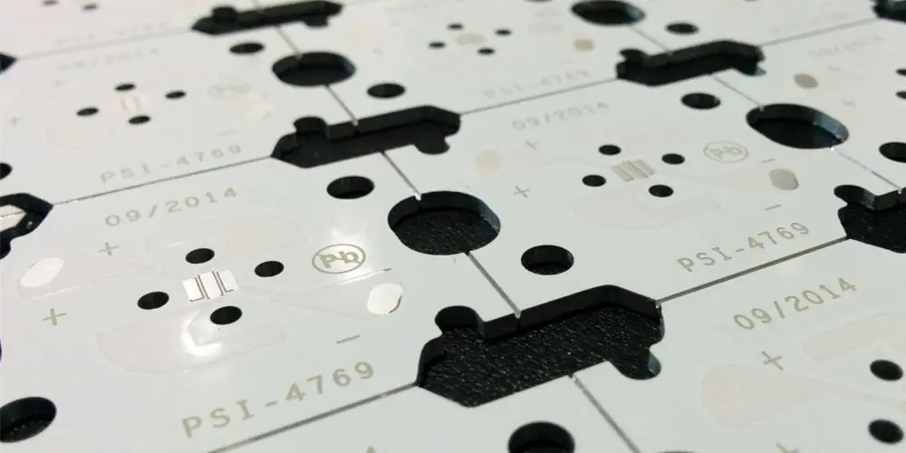
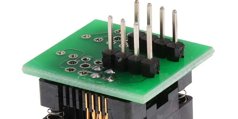
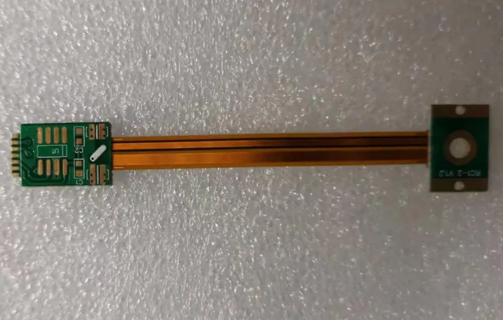
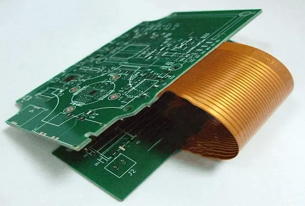
A flat, thin, piece of a dielectric material with conductive channels or traces carved on it is referred to as circuit card. These pathways link different electronic parts. Additionally, they are employed to link the parts to the sockets present on the circuit board. Circuit card assemblies are produced using the Circuit Card process of assembly. In this procedure, patterns are etched onto a specific dielectric substrate, like FR-4, and subsequently the substrate gets filled with different electronic components.

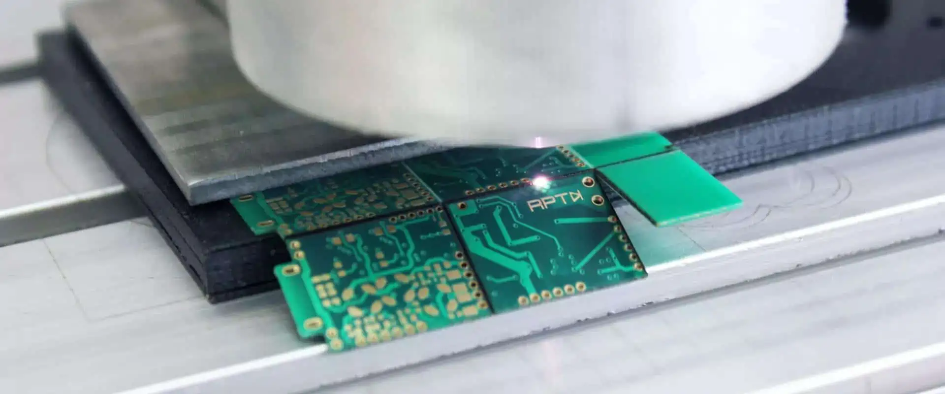
The creation of the design of the circuit card is the initial stage inside the CCA procedure. CAD software was used to make this design. When the design is finished, a CAM (computer-aided system for manufacturing) receives it. The design is used by this CAM system to offer the appropriate tooling paths as well as production instructions for such circuit card.

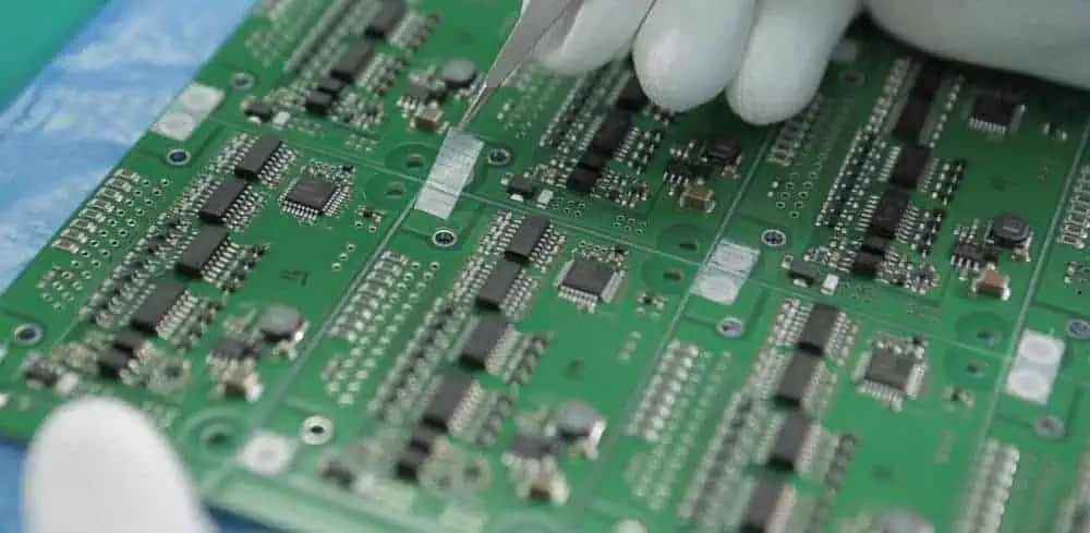
Etching this same desired patterns to the substrate is the following step. Typically, a photochemical method is used to do this. These electronic components are positioned upon that substrate as well as soldered immediately the patterns have been etched. This circuit card gets cleaned and quality-checked following the soldering procedure. It is prepared for usage once it has passed inspection.

What Does Circuit Card Manufacturing Entail?

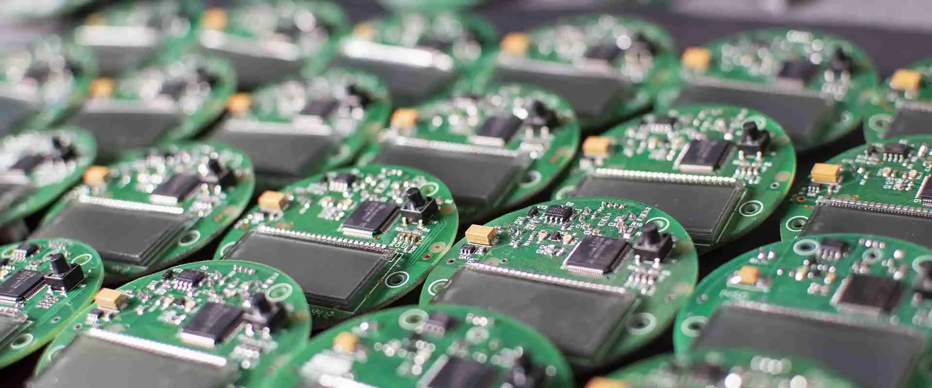
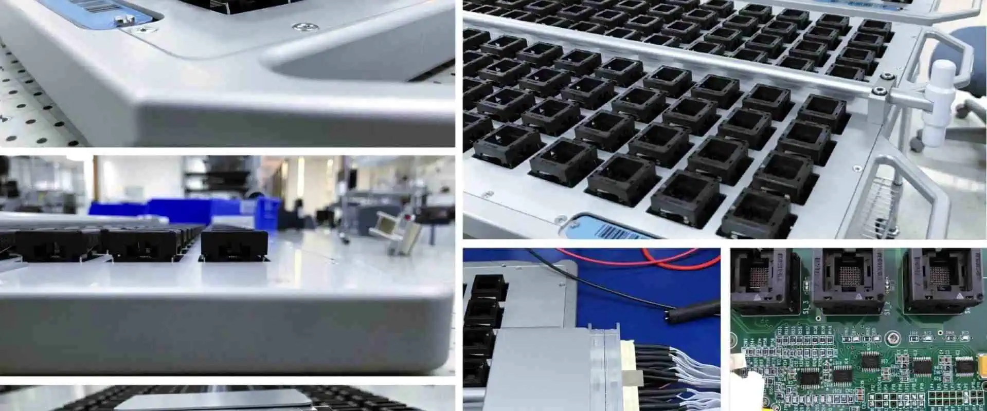
Through-hole and SMT machines are frequently used in CCA manufacturing to ensure the automation of the generation of CCAs. Experienced people are required to put out the design as well as assemble this type of production.

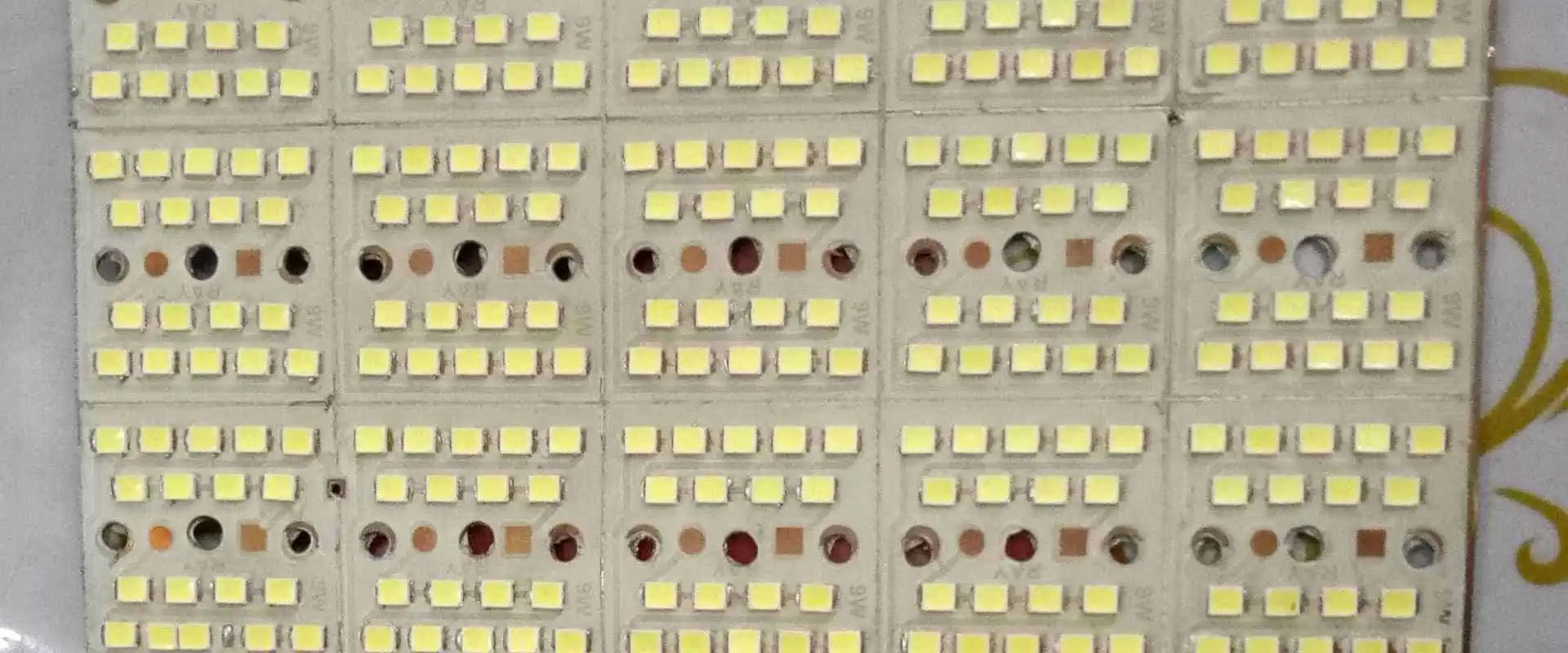
Circuit card assemblies, which are utilized in a variety of household appliances, including laptops, televisions, microwaves, Cellphones, smoke detectors, as well as security cameras, are similar to PCB assembly. Furthermore, they are utilized in a variety of sectors like monitors, power supply, vehicle displays, diagnostic imaging systems, including navigation systems.

Printed circuit boards are created through the fabrication of circuit cards. It is a process for producing PCBs from raw materials. It is utilized throughout a wide range of industries, especially aerospace and defense. The design plan for this form of manufacturing must be done by competent individuals, who must then layout this design coupled with assembling it.

What Components Make Up a Circuit Card?

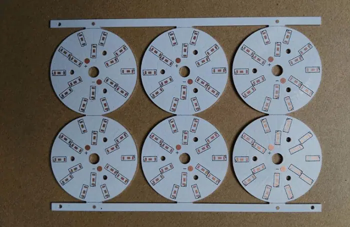
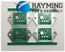
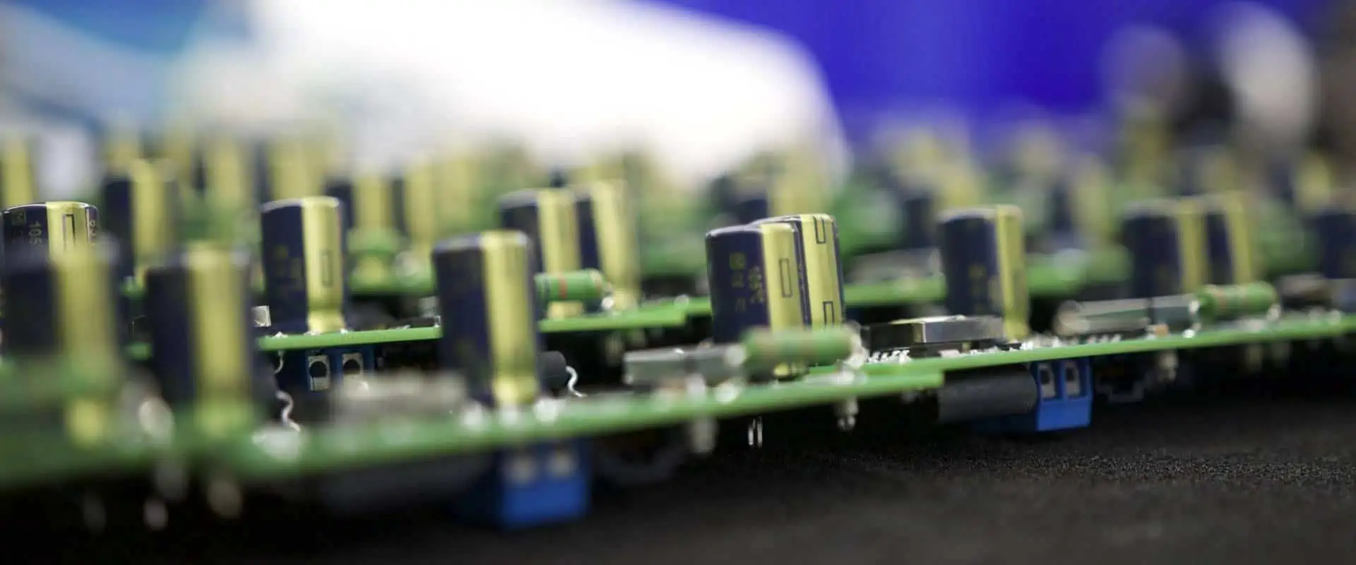
Many various CCA designs, capabilities, and types exist. Nevertheless, PCBAs are primarily made up of 4 fundamental components. These include: copper, a substrate, a solder mask, and silkscreen

Substrate

The substrate is the substance holding together all of the electrical parts. Depending on your PCBA type, substrates can differ significantly. You can get ridged, as well as metal core boards, for instance.

Copper

The PCBA’s substrate and a thin copper layer are bonded together, and conductive traces or tracks are utilized to connect various electrical components. Depending on the PCBA type, the copper layers might be multi-layer, double-sided, or single-sided.

Solder Mask

Like a coating for thwarting corrosion, solder masks are used to lessen the likelihood of the solder shorts. Additionally, circuit boards’ green or yellow color is a result of soldermask. In order to prevent corrosion and reduce the risk of a solder short, solder masks play a vital role as a form of coating.

Silkscreen

A legend listing the components as well as test points may be silkscreened onto circuit boards. ย The silkscreen is the final and top layer of all circuit boards. Element types which take the shape of texts or symbols are included in this layer. It helps engineers comprehend the board more fully. The silkscreen adds symbols, numbers, and letters to the circuit board.

What are the Electronic Components Present in the Circuit Card?

FULL PCB MANUFACTURING Quote

Diodes, transistors, capacitors, resistors, and inductors make up circuit cards. Now, let’s consider each of them.

Diode

Diodes can be described as a semiconductor device with two terminals that only allows for the straightforward current flow in a direction while obstructing the flow of current in the opposite direction. It functions as an electrical equivalent of the check valve due to this. A common application of the method is to convert AC into DC.

Capacitors

The creation of many electronic circuit types typically uses capacitors. The electrical component with two terminals that is passive called a capacitor has the ability to store energy electrostatically in the electric field. Considering that they may save electrical energy then thereafter transmit it again when necessary, they operate similarly like the rechargeable batteries.

Inductors

Two-terminal passive electrical components are known as inductors. Inductors, also known as reactors, save energy inside a specific magnetic field as electric current passes through them and discharge it back in to your circuit as necessary. While the Alternating Current is stopped by inductors, Direct Current can pass through them. It was discovered that when two inductors are placed opposite each other without touching, that magnetic field created by the initial inductor affects the second.

Transistors

One crucial component of the electronic circuit, transistors have transformed the area of electronics. Since over 50 years ago, these three-terminal, incredibly tiny semiconductor devices were manufactured. They are often used as components for switching and amplification.

Resistors

The resistor is indeed a passive component with two terminals that inhibits current flow. It is probably the simplest element in the electrical circuit. Resistance is one of the most often utilized parts since it is an important element in practically all electrical circuits.

Process for Manufacturing Circuit Card Assembly

Probe card pcb

What distinguishes fabricated boards from the assembled one?

A PCB’s fabrication and assembly are two distinct procedures.

The first step in the process of production is circuit card assembly, which begins with the design of the circuit board before being produced and tested. The flat sheet with insulating material as well as a layer of copper foil laminated onto the substrate make up the PCB during the fabrication. There are multiple layers to this flat sheet.

At this point, the circuit board is bare and seems to be a specific blank canvas! The device does not function because of any inductors, capacitors, resistors, or transistors. During the PCBA stage, components are usually soldered onto the board.

By attaching the components on the board, the process of PCB assembly turns the bare board into the functional unit. This PCB design must first pass the DFM review to confirm that it can indeed be produced. By doing this, costs are reduced and unforeseen delays brought on by design flaws that would necessitate re-engineering are eliminated.

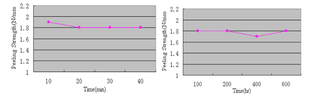
Are Circuit Cards Repairable?

Depending on the humidity, the amount of time used, as well as wear and tear which affects performance, the state of your Circuit Cards may deteriorate.

Consider the option of repairing your board before recycling your CCA. Before you start a repair, an engineering team needs to figure out why the board isn’t working properly.

Reasons Your PCBA Might Be Failing

Do you have a malfunctioning Circuit Card Assembly? Try to ascertain the root cause of the failure before you toss it away. You might still save your CCA by having it professionally repaired, depending on reason for the failure.

The following are some potential causes of problems with the circuit card: physical damage or harm, component failure, subpar design, trace damage, power failure, and other factors

Circuit Card Manufacturing Benefits

Circuit card assembly as opposed to alternative techniques of circuit card manufacturing, has a number of advantages. The fact that CCA enables significantly more complicated designs than the other techniques is one of its main advantages. This is so that CCA may connect the different components without needing to dig a hole.

As a result, more complex designs could be made without concern for physical drilling’s restrictions. The fact that CCA is a lot quicker than other approaches is another advantage. The entire process is carried out by one machine. This could save a lot of time because it eliminates the need to transfer a circuit card from a system to another.

Additionally, CCA is a highly economical way to make circuit cards. That’s because it produces the same amount of the circuit card assemblies significantly more quickly than some other methods, saving both money and time. The use of CCA has various drawbacks. One of the greatest drawbacks is that it could be challenging to repair the circuit card assembly created using this process.

This is due to how complicated the circuitry appears compared to other approaches. The difficulty of replicating a design is another drawback of CCA. This is so because the computer program was used to construct the design. It might be quite challenging to reconstruct a lost design.

Finally, mass production is not a good fit for CCA. This is due to how complicated the procedure is compared to other approaches. This indicates that this would be extremely challenging to manufacture several circuit cards utilizing CCA. CCA is a fantastic way for producing circuit cards overall.

Problems Frequently Found in Complex PCB Assembly

PCB prototype assembly suppliers

For the final product to work as intended, the circuit board assembly process entails a number of procedures and instructions that need to be followed in the correct order. PCB producers control he way components are put and secured into place by using regulated cooling and heating systems, screen templates, as well as other methods.

Depending on the available components, you must select the appropriate technology while assembling a circuit board. This PCB design calls for precise alignment of all the components in their predetermined locations. Any divergence, no matter how little, could have a significant impact on how well the final board performs.

What Does Complex PCB Assembly Mean?

The completed board once all the entire components are soldered and mounted on a circuit board is known as the circuit board assembly (PCB). The assembly is created by using the conductive paths carved inside the laminated sheet layers of copper of PCBs inside of the non-conductive substrate. The final step in creating an electronic gadget that is fully functional is attaching all electronic components onto the PCBs.

PCB refers to the circuit board that has not yet been assembled with electronic components. This board is known as the printed circuit assembly or a PCB assembly once the electronic components have been soldered on. Throughout this process, many automatic and manual tools for PCB assembly are used.

It is important to keep in mind that complex PCB assembly differs from the process of PCB manufacturing. Several procedures go into the production of circuit boards, including PCB design and PCB prototype production. Before a PCB may be utilized in different electronic devices or equipment, Passive and Active Electronic Components must be soldered on it. This electronic component assembly depends on the circuit board type, the electronic component type, and the circuit board’s intended use.

Technologies for Mounting during Complex PCB Assembly  

 SMT (Surface-mount technology)

The primary driver for the switch to SMT was the significant increase in PCB manufacturing process speed, cost, and reliability. Despite this being the main effect of the technology’s adoption, it also has an effect on the creation of fresh electronic devices and equipment.

Fortunately, the transfer has more positive effects on circuit performance and development than negative ones. The usage of SMT has various benefits for development engineers.

Components are put directly on the PCB surface using the SMT method. The technique, which was created during the 1960s but was initially called “planar mounting,” has become more and more well-known since during the 1980s. Nowadays, SMT is used almost exclusively in the production of electronic devices.

THT (Through-hole technology)

Component leads gets inserted in drilled holes present on the blank PCB for through-hole mounting. The procedure was used until the development of SMT during the 1980s, when it was anticipated that through-hole would be totally phased out.

However, despite suffering a sharp decline in popularity through time, through-hole technology still endured in the SMT era, giving a variety of benefits and specialized applications, most notably durability.

The optimum applications for through-hole components come with high-reliability systems that call for stronger connections present between the layers. Leads for through-hole components pass through the board, enabling the leads to endure greater environmental stress than SMT components, which are only fastened by solder and on the board’s surface.

Because of this, through-hole technology can be frequently applied to aerospace and military goods that could be subjected to high temperatures, collisions, and extreme accelerations. In test as well as prototype applications, which occasionally need for manual modifications and replacements, the through-hole technology comes also helpful.

Steps Necessary for Complex PCB Assembly

FULL PCB MANUFACTURING Quote

Stenciling of the Solder Paste

The first stage in PCB construction is the stenciling of the solder paste. This step stays the same regardless of the PCB assembly type. Over the circuit board is a unique stencil fashioned from a metallic and thin sheet. It makes sure that such solder paste can only be utilized where the mounting of the components is intended. The stencil is removed from the board after the solder paste has been applied.

Picking and placing the components  

Component mounting can be described as a picking and placing task that can be carried either automatically or manually. Component mounting is done by hand during THT PCB assembly. An automatic machine does it in the surface-mount circuit board assembly. Automatic mounting of the components provides a swift, accurate, as well as error-free procedure.

Soldering

On the Circuit board, soldering is used to connect components. Wave soldering is used in through-hole assembly. In this, a hot liquid wave solder is passed over a Circuit board with installed components. These solder balls become liquefied as a result, and the paste solidifies after cooling to room temperature. Reflow soldering would be done in the SMT PCB assembly, though. In this, a furnace with a 500ยฐF temperature is used to process the PCB.  After melting, this solder paste cools and settles with all the components involved.

Inspection

To guarantee that the gadget is operating properly, quality and inspection testing are done. It includes three separate inspection techniques, which are listed below.

Inspection (post assembly) as well as functional testing

After assembly, the PCBs undergo a second inspection and functional testing. To wrap up the process, functionality tests such as micro-sectioning test, solderability test, and contamination test are conducted.

Typical Issues with Complex PCB Assembly

PCB Assembly Control Board

Faulty PCB footprints

Just as we mentioned, it is crucial to verify the BOM so as to ensure the correct footprint is linked to the part. However, an examination of this PCB footprint must go beyond the BOM alone. Verify that this footprint is constructed correctly in accordance with the data sheet of the manufacturer as well as industry requirements.

Its footprint pads should also be examined to make sure the component will mount and solder to the PCB board properly.

Insufficient human access

Rework technicians cannot swap out parts, fix any assembly flaws, or test a board if they don’t have enough room to work. Due to the technicians’ need to maneuver around the impediments and potential for damage to other components, the limitation of space causes PCB assembly to take longer and cost more money. Additionally, if such connectors as well as other forms of human interfaces are not positioned for simple access, connecting the board to its system could be challenging.

Faulty soldering

The components must be positioned precisely to prevent soldering errors in addition to being properly spaced for the pick and place machine. The pieces must be rotated so as to enter a wave perpendicular towards it in order to use wave soldering.

Additionally, avoid placing taller components in front of shorter components in the wave since this may result in shadow effect, which may weaken the solder joint present on those pins. Make sure the two pins of the smaller 2 pin distinct items are both thermally balanced before placing them in solder reflow ovens. By doing this, you can prevent tombstoning, which is when a part gets pulled onto a pin because one side of the component heats up more quickly compared to the other.

BOM issues

Inaccurate information in the bill of materials may result in the ordering and installation of the wrong part on the circuit board. BOMs may also include information that is no longer accurate and list parts that cannot be produced.

Check the BOM of the circuit board before sending it off for manufacturing.

  • Accurate parts
  • Parts with matching part numbers and descriptions
  • PCB layouts that are accurately matched to their components
  • Parts that might not be readily available because they are end-of-life, obsolete (OBS), as well as recommended for brand new designs

DFM mistakes

One important factor for designing the circuit board is DFM – design for manufactureability. Make sure the components remain positioned with the appropriate distance between them, the board edge, and any other mechanical objects for the board.

Without this gap, it may be impossible to assemble the components using automated machinery, which would significantly increase the manufacturing cost and time of the board.

Faulty PCB footprints

Just as we mentioned, it is crucial to verify the BOM in order to ensure the correct footprint is linked to the part. However, an examination of that PCB footprints should go beyond the BOM alone. Verify that the footprint has been constructed correctly in accordance with the datasheet of the manufacturer as well as industry requirements. These footprint pads should also be examined to make sure the component will mount and solder to the pcb board properly.

PCB Inspection Methods in Complex PCB Assembly

pcba box build assembly

Visual and manual examination

Soldered connections can only be visually inspected by hand. This technique is only appropriate for small batches of Circuit boards; otherwise, optical fatigue prevents precision.

Automatic Optical Inspection

To examine PCBs, this AOI machine has high-resolution cameras which can be positioned at various angles. For the double or single-sized PCBs, this kind of examination is appropriate, however it is insufficient for multi-layer complex Circuit boards.

X-ray inspection

On complex PCB designs, X-ray inspection will be done. It is challenging to optically analyze such intricate PCBs.

Conclusion

More than the raw materials as well as a properly designed board are needed to put together the printed circuit board. It also needs the appropriate technologies. Additionally, there are a number of processes in the complicated PCB construction process that must be meticulously completed.

Why Aluminum Backed PCB is Suitable for Different Applications

aluminum backed pcb

Additionally, aluminum-backed Circuit board designs are very mechanically robust, making them well suited for usage in applications requiring a high mechanical stability level or are under significant mechanical stress. In addition, they are much less susceptible to the thermal expansion than buildings made of fiberglass.

What is Aluminum Backed PCB?

A PCB with an aluminum backing has a layout similar to every other PCB. Over it are one or more copper layers, solder mask, as well as silkscreen. However, an aluminum printed circuit board features a unique metal substrate rather than the fiberglass or the plastic one. Aluminum is the major component of this base.

This metal core may be composed primarily of metal and may include an aluminum and fiberglass composite. Although they could be double-sided, aluminum PCBs are mainly single sided. Manufacturing multilayer aluminum PCBs is quite challenging.

The majority of LED as well as power converter electronics utilize aluminum boards. Aluminum transfers heat away from the components as a result of the strong light that LEDs produce. The aluminum PCB increases the stability and longevity of the LED gadget. Aluminum substrates are used in domestic lighting, stop lights, and street lighting. They enable electronic regulation and current switching in power converters. Aluminum PCBs are used by designers in numerous other industries, however they are not used as frequently.

Additionally, designs of the aluminum backed PCB are very mechanically robust, making them well suited for usage in applications which need a high mechanical stability level or are under a lot of mechanical stress.

Layers of Aluminum Backed PCB

aluminum backed pcb board

These layers below make up the distinctive layered system known as aluminum PCBs.

Circuit Layer

This indicates 1 to 5 ounces thickness of the printed circuit foil. Copper foil makes up the aluminum board’s circuit layer. You can utilize the copper foils in weights ranging from one to about 10 ounces.

The Dielectric Layer

There are numerous solutions for dielectric layer that provide electrical isolation having the least amount of heat resistance. Additionally, it serves to bind the base material as well as circuit layer together. Each particular dielectric possesses its UL recognition.

The many materials we offer in stock are listed below to give you a wide range of choices with speedy delivery.

Base Layer

Copper or aluminum can be used as the foundation layer. Although there are many different thickness options, 0.040″ (1.0mm) is the thickness that is most frequently utilized.

Applications for Aluminum Backed PCBs

FULL PCB MANUFACTURING Quote

Using the aluminum boards will help your product last longer and perform better. For power as well as high-functioning temperature components, simple designs as well as low thermal resistance of the dielectric surpass all other insulators for circuit boards. The primary benefits of using aluminum for all these applications are its relatively lower cost than copper and its ability to provide lightweight material having exceptional durability.

Conversion of power

Aluminum clad is very dependable, compatible with different mechanical fasteners, as well as offer different thermal properties.

Circuit Boards for LEDs

Aluminum guarantees the lowest operating temperatures, maximum brightness, life, and color for the LEB PCB. We can provide our customers with the best solution since we have a wide range of inexpensive dielectric material options and specialized manufacturing tools intended for the single-sided manufacturing of the LED lighting product.

Motor Drives

That electrical isolation required to meet operational parameters as well as test requirements for the safety agency is provided by thermal-clad dielectric options.

Solid State Relays

To transfer heat from the vital system components, aluminum provides a particularly thermally efficient as well as mechanically sturdy substrate.

Aluminum boards are used in automotive industry because they require long-term dependability under harsh working conditions and temperatures as well as their need for proper utilization of space. They are usually utilized in the lighting components of automotives.

Items for consumers

Due to their light weight as well as small size, aluminum PCBs are most frequently used during street lighting, lights for interior building, lighting for traffic control, landscape lighting, as well as camping equipment.

What Types of Aluminum Backed PCBs Are There?

Aluminum Substrate PCB

As previously said, deciding on the aluminum pcb type depends significantly on your application. Below are the three primary categories of the aluminum PCB

Thru-Hole Aluminum PCB

This aluminum is usually pre-drilled for the thru-hole aluminum circuit board. A dielectric is then back-filled in the hole after that.

Flex Aluminum PCBs

Flexible dielectrics, which offer a high amount of flexibility, great thermal conductivity, as well as electrical insulation, are employed in these Circuit boards. Whenever these dielectrics are combined with aluminum, the resulting product is very flexible and could be formed into different shapes. With this, expensive fixtures and connectors will be eliminated.

Hybrid Aluminum Circuit board

These aluminum Circuit boards are typically employed in different RF applications. Also, they have a reputation for offering greater thermal performance whenever it is included into FR4-compliant products.

The Advantages of Aluminum Backed PCBs

Aluminum PCB Benefits

Aluminum boards are useful in a wide range of applications due to their many advantages. Here are a few advantages:

Light-weight

One of this PCB’s main benefits is that. Metals don’t get much lighter than aluminum. As a result, it aids in giving the PCB additional strength and resistance.

Heat-Removing Capability

When crucial circuit board components are subjected to extremely high temperatures, damage may result. Therefore, it is vital to employ a material which can dissipate heat in order to prevent them from harm.

The material that has the ability to transfer heat away from critical board components, shielding them from potential harm, is aluminum.

Long lasting

This aluminum is known as a strong and sturdy material with excellent durability. By employing aluminum backed PCBs, the possibility of unintentional breaking during handling, production, or regular use is removed. It can give a product more strength compared to ceramic and fiberglass bases.

Friendly to the environment

Aluminum backed PCBs are simple to construct, which promotes energy efficiency. In addition, the substance is non-toxic and recyclable. As a result, it is environmentally friendly. Therefore, it helps to protect the environment.

Conclusion

A finished product’s longevity and reliability in the long-term can be consistently improved by the aluminum-backed PCBs thanks to temperature management and accompanying cost savings.

The Purposes and Different Kinds of PCB Plate

PCB Plate

A circuit board’s successful operation depends on a variety of materials and parts. The majority of electrical gadgets are built on printed circuit boards. To design a circuit board, several materials are being used. One illustration of such a material is the PCB plate.

An essential part of the circuit board is the plate. Electronic gadgets benefit from the electrical and mechanical support provided by PCBs. Oftentimes, a plate is utilized in any keyboard PCB. We will go over all the details you should know regarding PCB plates in our article.

What Does the PCB Plate Offer?

The PCB plate can be described as a unique metal plate that is fastened over the keyboard’s PCB. This plate provides additional support.

Additionally, a keyboard’s keys are not installed directly on the Circuit board itself but rather on a PCB plate. Additionally, the keyboard’s PCB plate stops it from flexing. The keyboard may be made stronger and more stable thanks to this plate.

Larger keyboards typically use PCB plates. This can be attributed to the fact that  it provides additional help. Additionally, the additional size may cause the keyboard to flex more. However, the PCB plate is absent from some keyboards. Nowadays, keyboards come with a plate. Users have the option of designing a keyboard without a plate. The switches’ stability however, will depend on the quality of soldering.

The PCB can be described as the keyboard’s fundamental component. A keyboard operates using the PCB. Also, everything constructed on the keyboard begins with the circuit board.

The circuit board to the keyboard functions as the equivalent of a motherboard in a computer. When positioned on this PCB’s top, this PCB plate adds additional support.

This plate aids in giving the keyboard adequate stability. Additionally, it stops your keyboard from flexing.

Plate Material Types

PCB Plate board

The materials used to design a PCB ranges widely. Aluminum and Brass, however, are two materials used most frequently for the plates. Your choice will determine the kind of material that you are using for the plate. Explore these resources, though, and find what works best for your needs.

Brass

The brass plate is incredibly rigid. Brass is indeed a fantastic material that suits the PCB plate. But if neglected, this substance will eventually oxidize or tarnish. Some people claim that brass has a strong, bassy sound.

Carbon Fiber

The plate is quite robust and durable. Additionally, it is flexible and lightweight. Plates made from carbon fiber hence have a springy feel.

Aluminum

The most popular material for PCB plates is Aluminum. In both bespoke and prebuilt keyboards, aluminum plates were frequently employed. Furthermore, one material that is readily available is aluminum. This substance gives durability and is simple to cut. Keyboards made of this stiff material have no flex.

Polycarbonate

This material is plastic. Flexibility is possible and this polycarbonate plate could be bouncy whenever it is utilized. Users insisted that the plate had a form of bassy sound, though.

PCB Plate Applications

FULL PCB MANUFACTURING Quote

Keyboards are the primary application for PCB plates. When positioned on the top of circuit boards utilized for keyboards, these plates provide additional stability.

They are also applicable to switches that are plate-mounted. You need plates for these switches. Additionally, they have three pins on their bottom. Two forms of metal pins as well as a center circular knob are present.

They lack stabilizing pins though. The plate starts to serve its purpose at this point. As a result, every switch is stabilized by this plate, which also reduces side-to-side swaying whenever a key is pressed.

Plate Mounted Vs PCB Mounted Keyboard: Whatโ€™s the Difference?

This circuit board is present on both the plate mount as well as PCB mount. This same addition of the metal plate as support for the keyboard makes a significant impact, though.

Keyboards that are PCB mounted

Key switches on a keyboard like this will be placed directly to the Circuit board. The mounting plate is not necessary for a keyboard that is installed on a PCB. The smaller keyboards are the perfect fit for this mounting design. It isn’t the best solution for bigger keyboards, though. This is due to the resulting keyboard’s fragility.

It might not be worthwhile to use a plate mount technique on smaller keyboards. For larger or bigger keyboards, the plate mount seems to be the best option. The PCB mounted type of keyboard is also more affordable to develop since it allows more versatility. Keyboards installed on PCBs are fairly simple to alter. They are also less expensive.

Keyboards that are Plate mounted

Its key switches have all been mounted on the plate in this instance. Frequently, this metal plate gets mounted above the circuit board. Additionally, these key switches are mounted on top of the plate by the designer before being soldered onto the PCB. Designing the plate-mounted keyboard typically requires more time. Additionally, this mounting method takes more time and money.

Larger keyboards are acceptable for the design of the plate mount. It can also be a fantastic choice for the smaller keyboard. But the result would be a superior keyboard. Note that moving this mounting plate will be really challenging. As a result, making alterations or customizations might be exceedingly challenging. Therefore, it is recommended that you desolder any key switches before resoldering.

PCB Types Utilized for Keyboards

keyboard circuit board

Keyboard PCBs can be of a variety of sorts.

Through holes PCB

 5-pin Pcbs is a type of through-hole PCB. Here, using PCB plates is not required. It’s common for keyboards having through-hole Circuit boards to include build manuals. When utilizing this PCB, the designer will also have to solder some components, such as resistors. For more experienced keyboard makers with soldering skills, this PCB seems to be perfect.

Hot-swappable PCB

Hot-swap sockets are already fitted on this PCB. Additionally, this PCB enables switch installation without soldering or desoldering. As a result, it is the best choice for beginners. Additionally, you are not required to buy soldering equipment. Also, it is quite advantageous because it enables switching around different switches.

Soldered PCB

Customized mechanical keyboards frequently employ PCB that has been soldered. The switches must be soldered into the soldered PCB. Additionally, this PCB has 5-pin pockets which accommodates the switches. 5-pin switches are supported by the soldered PCB.

Conclusion

PCB plates in keyboards have a lot of useful functions. It is impossible to undervalue their significance. They are not present on every keyboard, though. This is dependent on the keyboard’s size. PCB plates provide a keyboard with more stability.

The Functions of the PCB Cutter in the Manufacturing of PCBs

PCB Cutter

In the production of electronics, PCBs are frequently utilized. These PCBs have a plethora of uses. Since PCBs were first used, these circuit boards have undergone numerous revolutions. The heart of electronic goods are the circuit boards. These boards also contain laminate materials and composite epoxy. There are numerous components on PCBs.

Cutting is the process of dividing an object to a number of pieces. When cutting, there is a force frequently used. One step in the fabrication of PCBs is PCB cutting. The PCB cutter is required for cutting.

What Does a PCB Cutter Mean?

The PCB cutter can be described as a particular kind of cutting tool that serves various PCB types. The cutter will cut PCBs varying in thickness from phenolic boards that are 2mm thick to thin aluminum and copper boards. A strong handle is another element of the PCB cutter. PCB cutters provide precise, clean cuts including an original design. To avoid any mishaps when working with the PCB cutter, you are advised to fasten a safety guard made of plastic.

Grade steel that is hardened comprises the lower as well as top shearing blocks. Hardened alloy makes up these blocks. They are strong as a result. A quality PCB cutter provides a clear, exact cut. To ensure accurate cutting, the user fastens a ruler onto that cutting platform.

What Does PCB Cutting Mean?

Cutting can be described as a technique that includes physically dividing a thing into its component pieces. Saws and knives are frequently utilized.

However, PCB cutting often involves the use of the PCB cutter. When the overall tension of these cutting tools exceeds the maximum strength of that thing being cut, then cutting occurs.

A PCB’s cutting procedure aids in producing the right board dimensions. Copper lines are another component of the circuit boards. A big PCB piece can be divided up into smaller ones. To get a good cut, you’ll need a reliable PCB cutter, though.

Various PCB cutting instruments are available for use during the process of cutting. A vital step before PCB cutting is preparation. The ultimate objective of the cutting of the PCB should be to produce clear and accurate cuts. As a result, it’s crucial to cleanly wipe the PCB using a very clean cloth.

You can remove debris and extra dust from the PCB by doing this. There are various techniques for cutting the PCB. A paper cutter for the tabletop or a Dremel are both options.

There are some safety precautions that must be taken when cutting PCBs. Wearing protective gloves is crucial when cutting the PCB. You won’t receive any unintentional cuts as a result of this.

Techniques for PCB There are two basic techniques involved in cutting PCBs. Cutting as well as sanding are some of these procedures. As was previously said, the ultimate purpose of the PCB cutting is to produce an exact and clean cut.

The Cutting of the PCB

FULL PCB MANUFACTURING Quote

Taking care is required during pcb cutting. You run the risk of spending more time and money if you aren’t diligent enough. You won’t need to invest more resources, such as time or money, which is included among the biggest advantages of getting an accurate cut. First, it’s crucial that you know exactly how big the PCB is that you wish to cut. To stop the PCB from slipping, place either of your palms on it. After that, you may pull its blade on the Circuit board firmly.

Sanding

After cutting the PCB, sanding is crucial. Most of the time, after cutting, people neglect to sand the PCBs. Additionally, sanding is a crucial component of Circuit board cutting. Your circuit board’s edge will get smoother as a result of this technique. Additionally, be sure to cleanly wipe that already-cut Circuit board to remove any dust or debris.

After cleaning the PCB, you can sand it. Use 200-grit or higher sandpaper while sanding. Make sure you sand its PCB’s edges until they are smooth. You can feel how smooth your PCB edge is by touching it. It’s crucial to wipe its edge with a damp towel after PCB sanding. Use the cloth to remove any oxidation or dirt.

Manual Hand Push Machine for PCB Cutting

For PCBs having a V-cut, a hand push PCB cutter (manual) is ideal. Additionally, this cutter runs on pressurized air. Additionally, this v-cut tool facilitates even-board operations. For splitting up large panels to tiny pieces, this cutter works wonders. It is a low-cost, easy-to-maintain cutter.

Additionally, using this kind of cutter comes very safe. It offers great safety and easy maintenance. A unique knob is also included for regulating the distance between the upper and lower boards. This cutter may be sharpened and used repeatedly.

The twin cutters as well as the upper round cutter are features of this hand push PCB cutter.

Considerations for Choosing your PCB Cutter

There are various types of PCB cutters. As a result, there are a number of things to think about while selecting the best PCB cutter for you.

high cutting precision

The PCB cutter’s cutting accuracy is crucial. Cutting precision varies across various PCB cutters. The cut’s precision is based on the PCB cutter’s accuracy.

Additionally, it will assist you in getting a very clean cut. Hence, it is crucial to choose a cutter having high cutting accuracy level.

low amount of noise

Additionally, you don’t desire a noisy machine. The perfect PCB cutter has very little noise. Some of the  PCB cutters are extremely noisy.

PCB components

The sort of PCB cutters you’ll choose will also depend on the substance of the Circuit board you plan to cut. For the FR4 boards, this hand push PCB cutter works best. When selecting a cutter, it’s crucial to take the PCB’s material into account. The sizes and thicknesses of PCB materials also vary.

Conclusion

An essential component of making electronics are circuit boards. These boards are produced using a number of procedures. Another of these procedures is PCB cutting using the PCB cutter. Therefore, this is crucial to comprehend this procedure. The PCB cutter is also required to get a clean and reliable PCB cut. Everything you needed to know regarding PCB cutting and PCB cutter has been covered in our article.

How EMS Companies Can Benefit From Electronics Outsourcing

through-hole assembly process

There has always been outsourcing in the industrial industry. For most businesses, attempting to build sophisticated goods from off the ground and up is simply inefficient. To benefit from the economies offered by specialization, numerous original equipment manufacturing companies collaborate with the electronics manufacturing service companies.

Of course, businesses outside of OEMs can also gain from outsourcing. EMS companies can also contract out the production of certain product components (CMs). Instead of controlling every step of the production process by themselves, this kind of relationship enables EMS businesses to concentrate on their expertise. Just as the OEMs gain from collaborating with you, your business can gain from cooperating with a CM.

What Services Do Contract Manufacturers Offer?

Sometimes the term “contract manufacturing” is used in a general sense; however, it comes with a unique function.

A CM expressly serves as the factory for their partners or employing company. They obtain the personnel, resources, and manufacturing techniques required to make certain products that are on demand. This opposes to other manufacturers, such as services for electronics production. The EMS will offer its customers engineering and production services for electronic products. Asides from  value-added services, several EMS companies also provide supply chain management and product development services.

To certain customers, several businesses might serve as both EMS and CM providers. These businesses provide contract manufacturing for customers who supply designs and give essential engineering support to others.

CMs may be crucial to the success of EMS businesses. An EMS may profit from outsourcing out some parts of sophisticated electronic assemblies. rather than reaching outsixe your major competencies, you could hire a contract manufacturer o help manufacture specialized components meant for your products.

Then you may use your resources to improve the core services offered by your company through research and design.

Why Outsource?

FULL PCB MANUFACTURING Quote

By reducing your market time through outsourcing, you can stay one step ahead of the competition and make sure that your clients receive their items when they need them. The distinction between a profitable or growing company versus one which lags behind its rivals is how quickly you can meet consumer demand. What strategic considerations cause an OEM to choose to outsource, then?

Defining the main tasks

In order to maximize the yield on their resources, all businesses may decide to outsource operations they may classify as non-core. Early on, businesses outsourced whatever they regarded as incidental tasks like cleaning, transportation logistics, as well as maintenance. What exactly is the essence of your business? This is what OEMs keep asking themselves?

Getting around capacity issues

Whenever an OEM somehow outgrows its facilities, struggles to find enough workers with the necessary skills, or requires to put some investment in fresh and upgraded equipment, capacity restrictions may result.

The sales team will need the tools and resources to manage new clients and meet the demand when your marketing initiatives have acquired significant traction and have increased orders. Maybe you’re in need of more money but have made the strategic choice to restrict your marketing and sales efforts out of concern that new businesses would clear off all your resources?

For businesses with lengthy sales cycles, whereby new activity could take months or even years to bear fruit, this could be a particularly difficult task. Numerous Financial Directors may find themselves in the difficult predicament of carrying extra overhead layers to respond to unforeseen demand.

However, what other options are available? Run your business more efficiently and then expect to hire more workers whenever the sales start to pour in? What if you’re having trouble locating the appropriate individuals with the necessary abilities just when you desire them most?

It can be difficult to fully let go of the security these extra expenses offer. An OEM might have to consider its options and its strategy as well as consider outsourcing seriously if the overall demand level is rising yet it is unable to or unwilling to raise its capacity.

Enhancing cost management

How much actual control have you over your expenses?

A genuinely set unit pricing for items is a major advantage of outsourcing manufacture. Outsourcing excess demand may be motivated by capacity restrictions, but what of the cost impact that are less than anticipated? It is debatably simple to determine a product’s cost at the unit level. It is as easy as counting the hours required to put it together and then multiplying that amount by the labor rate per hour.

Similar principles apply to materials; all that needs to be considered is the product’s direct material cost. While this might be a great issue to have, if demand rises, it could need extra capital expenditure.

But what would happen to costs if demand decreases? On the surface, the cost appears to remain constant, but in reality, the unit cost seems to be quickly rising due to the underutilization of your procurement and production labor, as well as related resources like space as well as capital equipment.

This doesn’t occur in outsource models. The unit pricing remains the same whether you purchase 10 items in a week or you decide to purchase 40 the following week. Because of its agility, the EMS company can deliver goods on schedule while minimizing the financial impact of shifting demand patterns. The same agility and response that you’d anticipate from your shop floor are also present.

Additionally, cost savings on its own might not be sufficient to outweigh the risks as well as difficulties of outsourcing that must be evaluated, viewed, and given equal weight with the other important business metrics like improved quick deliveries, decreased lead times, higher cash flow, as well as the prevention of future investments that are asset related.

How close should you get to full outsourcing?

In general, it is sensible to outsource quite enough work as you can to a subcontractor because you will gain the most from doing so. However, some of this build process’s technical features might need to be kept in-house.

Consider the case when your product analyzes minute gas particles in a unique testing setting. Most likely, you’ve created specialized equipment to manufacturer as well as test this specific item.

An outsource partner may find it impractically costly and time-consuming to duplicate the necessary tools or processes. It might be more practical in this situation that you handle that aspect of the construction process yourself.

No charge or complete procurement

The decision of whether to do a free issue and even have the EMS partner purchase all the necessary materials is another important one at this point.

One way, the free issuing enables you to keep full or partial control over your component procurement procedure. When outsourcing manufacturing, certain organizations may feel that it is important.

Free issuance, on the contrary hand, poses a variety of obstacles to the overall advantages of outsourcing. Potential cost-saving benefits are diminished because you need to maintain an infrastructure to manage a supply chain as well as a warehouse for storing stock.

In addition, when you outsource, you frequently add an additional complexity layer at a time when you’re attempting to make things simpler. You are in charge of ensuring that all portions are original and readily available at the appropriate moment when you decide to free issue the material. Delivery times are impacted and major delays are caused by missing, damaged, or incorrect components.

An effective subcontractor would have some end-to-end procedures in place so as to smoothly combine supply chain management with assembly line demands. Always keep in mind that the entire business of a subcontractor is centered on manufacturing; and this is exactly what they do 24/7.

Simply said, it makes perfect sense when you outsource to the subcontractor as often as possible. Free issue has few benefits and many possible drawbacks.

What are the Advantages of Outsourcing your Work to the Contract Manufacturers?

pcb-assembly-san-jose

For services related to electronic manufacturing, CMs can offer a number of distinct advantages. Outsourcing can do more for your business than just make your manufacturing more accessible; it can also help you save money, generate better products, as well as expand more quickly. The following is how it offers such advantages:

Lowering labor and fixed costs

You must control both labor and fixed expenses in order to manufacture all components of your devices. As the EMS, the creation and assembly of sensitive electronic equipment is the primary focus of your production facilities. Maintaining a second site with wholly distinct requirements increases the location costs as well as necessitates hiring people, which will greatly increase your expenditures.

You completely avoid those fees while dealing with the CM. The factory and its employees are already at the CM’s disposal. Since many CMs collaborate with numerous employing firms, they enjoy cost savings in terms of hiring and manufacturing expenses. You receive it, enabling you to direct your attention elsewhere.

Increase in Scalability and Flexibility

Whenever the company manufactures its components, expansion requires a lot of time and money. There’s a need to foresee the future demand as well as make an independent attempt to construct additional infrastructure to help support it. Flows and ebbs in orders, meanwhile, might be difficult to handle. When demand is low, you must still cover the fixed costs. Also, when the demand is strong, you risk running out of resources, without the opportunity to have more.

Collaborating with the CM enables your business to become more adaptable as well as scale more easily. Your company doesn’t have to maintain excess capacity because the CM does. You would be able to collaborate with your CM as the main manufacturer or in the overflow capacity. In either case, you can scale your firm considerably more quickly and adjust to changes in demand.

Increasing effectiveness and quality

CMs have a focus within their disciplines. A good CM does have the know-how and infrastructure ready to ensure high-quality products. After all, the particular components you will be outsourcing are the CM’s area of expertise. You can benefit from a CM’s complimentary skill set by hiring one.

Because of this, outsourcing to the CMs is also more effective. Reinventing the wheel is a waste of resources and time. Instead, you may rely on your contract manufacturer to give you top-notch goods while you concentrate on delivering your personal services.

How Contract Manufacturers Work With EMS Companies

Many EMS providers already collaborate with contract manufacturers. These businesses discover that outsourcing enables them to keep their attention on their core competencies while growing their skills and offering more services.

For instance, NAI recently collaborated with a Chinese company involved in mining manufacturing to enhance interconnect production. Furthermore, t he business needed to make its specialized mining operations’ electronic components more dependable and long-lasting. Custom harnesses as well as housings for unusual circumstances were not within the scope of the company’s expertise because equipment for mining control was its area of expertise.

Because the company required to house sensitive electronic components, such as controllers and inverters, in a high-risk, high-stress environment, NAI was selected as their manufacturer. NAI was the best CM for this Chinese company to outsource manufacturing to because of its experience producing goods for both telecom and industrial applications.

Working together has only produced positive outcomes for mining projects. By collaborating with NAI to serve as its CM, it has been able to lower safety risks associated with its operations, get access to NAI’s worldwide supply chain, and benefit from more productive manufacturing to shorten lead times. T he company’s first outsourcing arrangement was so effective that it increased its cooperation with NAI so as to include more projects.

Utilize the Advantages of Outsourcing

Providing your customers with high-quality equipment should be your company’s first focus. However, there is no reason why you must manufacture each component inside. You may streamline the production of your company while preserving the finished product’s quality by working with a reliable CM who has a history of producing high-quality work. Synergies between the company and the contract manufacturer will benefit you in terms of efficiency and cost.

Any EMS seeking expansion, adaptability, and cost reductions should think about outsourcing manufacturing. Concentrate on your areas of expertise and delegate anything outside of them to a reliable CM. The advantages of your relationship will become apparent right away.

Steps Involved in Custom Electronic Assembly

Subcontract PCB Assembly

When putting together custom electronics, your application needs to be clearly defined. Off-the-shelf controls’ flexibility may be a preferred idea if this functionality is anticipated to evolve over time. However, if such functionality is clearly specified, you may construct and design a unique control system which only comprises the required hardware and software that will typically result in a smaller, more straightforward, and cheaper solution.

PCB and circuit design costs are added to your engineering efforts in this choice, thus it is necessary to compare them to their per-unit savings.

What Does Custom Electronic Assembly Entail?

High-Volume-PCB-Production-and-Assembly

Tech enthusiasts recently have become much more self-reliant. Downloading software and making changes to our devices to make them the manner we require them has gotten simpler. Many people have mastered the skills necessary to create their personal websites, create mobile applications from the ground up, or engage in other types of programming language exploration.

People have increasingly grown accustomed to purchasing, personalizing, and arranging goods and technology in order to improve their surroundings. This is exactly what has ultimately caused the fueling of the explosive growth of smarthomes and some other developments that equate to technology enhancing as well as automating our surroundings.

We don’t give any of these adjustments much thought. We develop with technology, and when it becomes a bit simpler in some ways, we become more at ease with customizing it to our needs.

The process of creating your personal electronic items, however, needs a little more expertise and deliberate effort. But tech fans are also beginning to enjoy this as a hobby more frequently.

Along the route of designing the electronic subsystem for new smt machines or products, you will have to make a lot of make-or-buy decisions. These choices are based on a number of variables. These include functional requirements, per-unit cost, upfront engineering cost, required quantities, size and form factors, timelines, security concerns, and intellectual property concerns.

Steps Involved in Custom Electronic Assembly

FULL PCB MANUFACTURING Quote

The process involved in the conversion of PBCs, or circuit boards, into the PCBA, or circuit board assembly, is known as custom electronic assembly. The connection of electrical components onto a circuit board accomplishes this.

Electricity is connected between points A and B via a large number of tiny circuits, each connecting electricity of a distinct frequency and intensity. PCBAs a re utilized in numerous different electronic devices after the process of electronic manufacturing. The procedure of assembling a custom electronic consists of 5 important steps.

Printed Circuit Board (PCB)

Starting with the circuit board as well as the components which belong on it, you can assemble custom electronic devices. This circuit board can be described as a little board.

Apply solder paste

A screen-printer is used to apply paste on printed circuit boards after having it. To ensure that the solder paste will only coat the board where required, then you make use of a thin stencil.

Pick-and-Place

The parts are then positioned onto the printed circuit boards. A device known as a Pick-and-Place performs this by picking up the components and placing them upon that circuit board where they belong. What this machine can’t handle, a technician completes manually.

Inspection

Following the assembly of your circuit boards, it undergoes an AOI (automated optical inspection) procedure to ensure that all of the components are in their proper locations, are orientated appropriately, and are not missing.

Soldering

This PCBA is placed into the oven as the first stage in the process of custom electronic assembly. Metal microbeads in the paste are melted in the oven. This metal melts then solidifies as a single connection piece when this paste heats up.

How to Create Custom Electronic Assembly

It’s difficult to create a brand-new technological equipment from scratch. Particularly if you’re a startup or entrepreneur with little or no experience in electronics engineering or design, this process could first seem overwhelming.

This should not deter you from developing your ideal product, though. You may quickly build a working prototype by reducing the process into some few easy phases, which could then be utilized to attract more funding or venture funding.

Make your schematic diagram

Making a circuit diagram for your product is the initial step. This serves as your product’s conceptual design.

You will have to select the appropriate topology and relevant components at this point. You can hire an electronics professional to do this phase if you are lacking the necessary knowledge in electronic design.

You might want to make your schematic if you have any experience with electronics engineering. Various software packages exist for this, but DipTrace is our top pick for smaller applications. This low-cost software package is simple to use and has the ability to create and simulate intricate designs.

Designing your PCB Layout

This PCB layout needs to be made after the schematic has been designed. This is also possible in DipTrace. The layout can also be created from the schematic by your circuit board manufacturer.

If you plan to design the PCB yourself, you must get a specs document from the PCB supplier. Trace spacings, wire widths, and other requirements vary according to the manufacturer. Therefore, you must take this into account in the PCB design.

Analyze and Debug

After designing your PCB, you can make the prototype board. You can then assess and debug your product in the most fundamental form. At this step, you will typically discover a few problems, but keep calmโ€”this is clearly a typical occurrence in the process of development. Just solve each issue one at a time till you’re satisfied.

Program your microcontroller

pcba box build assembly

These days, the brain of the majority of devices is a microcontroller. This is typically programmed in “C,” however if you require a device to be really efficient, you might want to think about using Assembly language. Again, if you lack the necessary programming skills, you could outsource this stage.

Creating your Prototype

It’s now time to design a functional prototype. Using the CAD software, start by making the device’s 3D model. This will help you develop realistic costings and reveal to you the way the completed design will appear. Nowadays, 3D printing is used to create the majority of prototypes. However if you contract out this stage to another industrial designer, pick one with knowledge of both 3D printing and injection molding.

Inexperienced designers frequently produce 3D models that are appropriate for the 3D printing however can’t be injection molded.

Considerations for Custom Electronic Assembly

In order to meet their business goals, companies constantly evaluate their product roadmaps, create projects and timetables, allocate resources, as well as set budgets. It is crucial to fully comprehend the numerous aspects involved in constructing the electronic products as well as acco

Benefits, Limitation, and Applications of Customized rigid flex PCB

Customized rigid flex PCB

For over forty years,Customized rigid flex boards have been used in the high-performance applications.  PCB integrates layers of rigid and flexible materials to create rigid-flex boards. Also, copper plated vias connect rigid outer layers with inner flexible layers.

What is a Rigid-flex PCB?

A Rigid-Flex PCB is a type of printed circuit board that combines both rigid circuit boards and flexible circuit boards. This board can be folded, bent, and twisted.  This continuously flexed into any shape or curve during manufacturing. Furthermore, the flexible layers of this board are usually buried within the board. These layers penetrate through the rigid part of PCB.

Rigid-flex boards offer the flexibility of flexible PCB and durability of rigid PCB. These boards are very resistant to harsh application environment. Therefore, it is widely used in the medical and military industries. Rigid flex boards are different from flexible printed circuit boards or rigid printed circuit boards in terms of material and manufacturing process.

For over forty years,Customized rigid flex boards have been used in the high-performance applications.  Rigid flex PCB manufacturers integrate layers of rigid and flexible materials to create rigid-flex boards. Also, copper plated vias connect rigid outer layers with inner flexible layers. Customized Rigid flex circuits offer more quality control and higher component density. Rigid designs are needed where there is requirement for extra support for SMT components while flexible designs are required in applications that need to flex and bend to fit into tight spaces.

Rigid-flex circuit boards provide optimum solutions for limited space conditions. These boards provide secure connection of device components while ensuring contact stability and polarity.

Benefits of Customized Rigid Flex PCBs

rigid-flex-circuit-boards

Rigid flex PCBs offers a lot of benefits which include:

Connection reliability

The foundation of Customized rigid flex PCBs lies in the connection of rigid layers with flexible cables. The combination of rigid layers and flexible layers gets rid of the need for wiring harness to connect rigid boards.

Lower part count

Rigid flex circuit boards need fewer interconnections and parts compared to  traditional rigid boards. Therefore, they reduce the number of parts through the elimination of board-to board connectors and wire harness.

Flexible Design Options

The integration of flexible and rigid substrates in Rigid flex circuit boards made it easy for these boards to meet the requirements of highly complex and unimaginable configurations. Also, rigid flex circuit designs can integrate the following:

  • Controlled impedance
  • Reduced interconnections
  • Highly complex configurations
  • High layer count

High density applications

Customized Rigid flex PCB helps to free up space by getting rid of interconnecting hardware. Therefore, this enables for greater connection density.  The rigid parts of a rigid flex PCB are usually integrated for populating high density SMT devices. On the other hand, the flexible layers help to connect the rigid areas and as such, allows the circuit to be in a 3-dimensional shape. This circuit has several interconnected rigid areas on various planes.

Weight Reduction

Flexible circuit materials have very thin nature and they can create very narrow circuit traces. All of these make it possible to achieve higher connection density with a reduction in overall system weight.  The low weight of rigid flex boards makes them suitable for use in extreme shock and vibration applications.

Applications of Customized Rigid Flex PCBs

FULL PCB MANUFACTURING Quote

Automotive industry

The automotive industry keeps experiencing new innovations and developments. Energy vehicles are the future development of this industry. Automotive wiring harnesses are quite complicated in connection. This doesnโ€™t work well for the increasing quantities of electronic components required in new energy vehicles.

However, rigid flex PCB is an ideal replacement for wire harnesses since it offers design flexibility while being able to tolerate several dynamic bending without causing any damage to the wire. Furthermore, rigid flex boards offer a level of flexibility and rigidity which is ideal for automotive electronic components in extreme environmental conditions. Customized Rigid flex boards are widely used in the automotive industry. You will find them in car display, navigation and entertainment system.

 Medical Wearables

In recent years, wearable devices have gained popularity in the medical field.  Wearable devices like smartwatches and fitness trackers have been widely integrated to track peopleโ€™s health and general well being. There are other wearables like smart clothes.

The advancement in technology has been a great help in the medical industry. It is crucial for medical practitioners to keep track of their patientโ€™s wellbeing. This could involve monitoring a patientโ€™s breathing patterns and heart rates. With the advent of wearable devices, medical professionals can get information about patients’ health regardless of where they are.  

Most wearable devices integrate flex-rigid boards. Since these devices need to be compact, they require the integration of flexible and stiff components. Also, wearables must be able to operate under the stress of everyday activity. The integration of rigid layers offers the reliability that needed for these electronics to function in demanding situations.

Rigid Flex PCB Design

Rigid-Flex PCB
Rigid-Flex PCB

Guidelines for Rigid Flex PCB Design

One of the important stages of rigid Flex PCB manufacturing is the design stage. The design stage lays the foundation of the Customized rigid flex circuit. Therefore, it is crucial to understand some main elements during the design stage.

Rigid flex PCB designers need to adhere to laid down rules throughout the design process. Ensure the PCB corners aren’t bent when making them.

 If at all you need to make a bend, make sure the bend is curved. Change the trace width gradually when doing so. This is because abrupt changes can result in a weak spot. Therefore, making use of at least two flex layers will enhance flexibility and as well reduce costs.

Guidelines for Rigid Flex PCB Layout

There are certain guidelines you need to maintain when creating a rigid flex PCB:

Trace Width

Ensure the trace width calculator delivers correct results for the trace width and spacing between its flexible parts. Furthermore, ensure the solder pads are completed in rounded styles.

Soldering Surface and Annular Rings

Rigid flex designers must ensure the annular rings and soldering surfaces are large enough. Stiffeners can help you to achieve the required thickness. However, you can apply coverlays on the flexible parts of the rigid flex PCB. This provides the conductors with protection and insulation.  Cover lays are crucial during soldering as they restrain and hold the pads.

Also, the PCB manufacturer must ensure there are anchoring spurs on the pads. This helps to ensure a good bonding between the material and the copper during the rigid flex PCB assembly process.

Vias

Ensure the plated vias are metalized. You can achieve this through the drilled holes. The holes connect conductive layers and flexible circuit. There must be connection between the blind vias and its inner layer. Also, you can integrate the buried vias. The buried vias and blind vias help connect the internal layers.

The integration of various types of vias will augment any space present in the circuit board. Also, this enables the addition of various component pads. This space helps in trace routing. Also, designers need to pay careful attention on accuracy when you calculating the bending radius of rigid flex PCB. This helps to prevent breakages.

Steps Involved in Designing the Rigid Flex PCB

Rigid flex PCB
Rigid flex PCB

There are several steps involved in Customized rigid flex PCB

Base material preparation

Before the fabrication process, the laminate must be thoroughly laminated. This process is very important, this is because copper coils have anti-tarnish features.

In this step, the copper coil will need to be dipped into an acidic solution. Alternatively, you can use the spraying method. After this, you can use various oxidation agents to coat the coil in an extensive manner.

Circuit pattern generation

This step involves the creation of circuit pattern. There are two major techniques for this; screen printing and photo imaging.

The initial method can help you generate the right circuit patterns. Screen printing can deposit on the surface of the substrate. The photo imaging technique is widely used. Also, this helps to ensure the dry photoresist film deposits on the substrate.

Etching

Etching involves dipping the substrate in an etch bath. Another method is using an etchant solution to spray the substrate. You can etch on the two sides to get the necessary results.

Drilling

In printed circuit boards, the holes,  pads, and vias are usually drilled.  Ensure your drilling tools can sustain a high speed. This will help you achieve precise holes. Also, it is advisable to create very small holes with laser drilling.

Through-hole Plating

Customized Rigid flex PCB manufacturers need care and precision in this step. After the hole has been drilled, the manufacturer will need to deposit a good amount of copper in it.

Cover Lay or Covercoat application

The next step after through-hole plating, the application of cover lay or Covercoat is the next step. Doing this will protect the bottom and top sides of the rigid-flex circuit. This will as well protect the circuit from all hostile environments, and solvents.

Types of Rigid flex PCB

rigid-flex pcb
rigid-flex pcb

Single sided Rigid-Flex PCB

Single sided rigid flex PCB features only one conductive layer. The other side of this board enables the integration of various electronic components on your PCB. Furthermore, single sided rigid-flex PCB compromise a single layer of rigid and flex substrates. This PCB is easy to manufacture compared to the other types of Customized rigid flex PCB.

Double Sided Rigid Flex PCB

Double sided rigid flex printed circuit board comprises one single rigid substrate layer and another layer of a flexible substrate. The flex layer provides flexibility while the rigid layer helps to enhance compactness.

Furthermore, double sided rigid flex printed circuit enables more routing traces. Double sided rigid flex boards are highly preferred among PCB engineers since they offer enough flexibility. Also the capability of this board helps in minimizing the board size.

Multilayer Rigid-Flex PCB

The multilayer rigid flex circuit board has at least three conductive layers of rigid and flexible substrates.

Limitations of the Rigid Flex PCB

Now that we know the benefits of Customized rigid-flex boards, let’s discuss some of its limitations.

Elaborate Manufacturing

Rigid flex PCB manufacturing require the integration of two substrates, one rigid layer and one flexible layer of substrate. The integration of these two substrates increases the time spent on production.

Labor intensive production

ย Rigid flex PCB manufacturing is both material intensive and labor intensive This is because of the variations and the sensitive nature of this antenna PCB.

Complex manufacturing process

The manufacturing process of the Customized rigid flex PCB is a complex one. It is different from the manufacturing process of other simpler PCBs. Also,  this process requires the use of effective software. These factors contribute to the high cost of production.

Rules for Rigid-flex PCB Design

Rigid-flex PCB Board

It is important to adhere to certain guidelines during rigid flex PCB design and manufacturing. These guidelines can serve as a checklist.

Make prior decision materials and manufacturing processes. This decision should be based on how much โ€˜flexโ€™ your board requires. For example, if you are designing the circuit boards and you only need to fold them during the manufacturing process. You have to choose wisely:

  • Number of layers
  • Type and grade of copper
  • Manufacturing method

However, if this circuit board is meant for applications exposed to extreme shocks and vibrations, you need to decide on:

  • Adhesives
  • Copper coils
  • Number of layers

You should place copper traces to the circuit’s right angle since they work well when they positioned at the board’s right angle.

Therefore, it is crucial to stop bending at the corners. However, there are some considerations for PCB design that require bending at the corners. Use hatched polygons to retain the flexibility of the board.  The integration of solid copper pours may minimize flexibility.

Copper can remove from the polyimide substrate because of the repeated stress from frequent bending. However, you can prevent this from happening by providing enough pad support to the exposed copper traces. Most times, the integration of surface mount pads is ineffective for this purpose. But, the use of anchoring stubs and coverlay openings can improve the pads’ reliability.

Conclusion

Flexible PCBs and rigid PCBs are different from Customized rigid-flex PCBs. Rigid flex printed circuit boards combine both flexible circuits and rigid boards. These boards are ideal for use in a wide range of applications.

Altium Designer 19 vs Altium Designer 18: What are the Differences in their Functionalities and Features?

Altium Designer 19 vs Altium Designer 18

Altium designer is one of the most popular PCB design software. This software comes with a lot of easy-to-use tools and advanced features that help you achieve an efficient PCB design.  Altium LLC keeps releasing new version of this software every year. This new version is usually equipped with more enhanced features than the previous versions. In this article, we will be discussing Altium designer 19 vs Altium designer 18.

What is Altium Designer 19?

Altium designer 19 has continued to offer new features and advancement to its core technologies, while providing solutions to several problems encountered by customers. These problems have been stated through the BugCrunch system  of the AltiumLive Community.

Altium designer 19 doesnโ€™t only offer a wide range of new advanced features, but it also integrates a large number of advancements and fixes across the software as a whole. Therefore, this helps designers to keep creating cutting-edge electronics technology. Altium Designer 19 was built on the consistent reliability and functionality of previous versions. This version features modern designs that are easy-to-use and powerful.

Furthermore, users can have access to a connected and convenient design experience where everyone is in sync via seamless connectivity. This version leverages powerful EDA technologies with the main focus on improving the experiences of users. Also, there are new capabilities that model high-density interconnect structures. Therefore, this makes designers confident when producing quality high-density circuit boards.

Altium designer 19 is an advanced PCB design software applications which enables designers to create great designs. The improved PCB materials library helps users to create impedance profiles for manufacturing and routing. Furthermore, there is an optimized component panel in this Altium version. This version of Altium Designer is a great investment into cutting-edge designs.

Features of Altium Designer 19

Altium Designer 19
Altium Designer 19

The Altium designer 19 comes with a lot of advanced features and improved functionality which include:

Advanced interactive routing tools

The advanced interactive routing tools have many tools like glossing pushed routes, move component, and follow mode during interactive routing. The designer will need to make adjustments to the location of a component so as to make space for new routing. You can move a component with the routing-friendly move component.

The improvements on interactive routing include junction smoothing, loop removal, gloss control, and differential pair zip up. With the junction smoothing tool, you can carry out automatic corner reshaping to prevent acute angles.

Structural electronics design

One exciting advancement in Altium designer 19 is the capability to directly print the electronic circuit onto a substrate like a plastic molding that is part of the product. This capability is a great evolution in the design and manufacturing of electronic products. Printed electronics enables electronics to be fully integrated into new markets.  

This new release supports the design of printed electronics. With the integration of printed electronics, designers will no longer need the rigid fiberglass PCB substrate. Printed electronics allows the circuit to directly form as a part of the electronic product.

Components panel

The components panel was strictly developed to replace the previous Libraries panel. This tool offers direct access to all components, which include Managed Components that are on the connected managed content server. Also, the component panel comprises the related data for a chosen component.

Furthermore, the components panel has the new parametric search capability. This search capability enables users to easily locate the part needed from the component resources of your company. Also, this tool makes use of the basic search engine view applied in the Manufacturer Part search panel.

ActiveBOM

FULL PCB MANUFACTURING Quote

The ActiveBOM transitions the selection features of the supplier-centric component to manufacturer-centric component selection. Furthermore, the activeBOM offers support to auto MPN and user-defined ranking in the BOM items list. Therefore, this makes it much easier for a designer to monitor the order of the solution for every part.

Another benefit of the ActiveBOM is that it carries out real-time checks on items included in the BOM. The ActiveBOM can directly add BOM items in the BomDoc. This is a great feature for items not needed on the schematic. Also, this feature supports Supplier Links. The Supplier Links always include the supplier details and are added to the schematic components.

The ActiveBOM allows users to

  • Make changes to a component in the BOM, and then push that change back to the project through an ECO.
  • Rank the Part Choices
  • Carry out BOM Check validations from the OutputJob.
  • Integration to the new BOM Report Manager.

New part search panel

The new part search channels allow users to easily research, choose, and source the appropriate parts for a circuit board design. This new tool has replaced the Part Search panel. To provide the best component parts, the new part search panel integrates the data sources of the Altium Content vault and Altium Parts Provider.

The Manufacturer Part Search panel comprises a set of data for component parts, which includes associated models, part supplier links, and manufacturer parameters. The search engine of the panel provides users with an adaptive range of filters and a graded listing. This helps to easily discover the part needed.

New Features and Enhancements in Altium Designer 19

The new features and upgrades in Altium designer 19 can be summarized as follows:

  • Enhanced interactive routing tools
  • Faster multi-board design
  • Improved layer stack manager
  • Microvia support to house high densities of advanced component packages
  • Printed electronics support
  • Draftsman enhancements

What is Altium Designer 18?

Altium Designer 18

Altium has kept on focusing on the development of cutting-edge design features that meet the requirements of todayโ€™s design. The Altium designer 18 is a powerful and easy-to-use PCB design software. This version offers performance enhancements and key updates alongside advanced features. These advancements help in increasing design productivity.

Altium Designer 18 aims at providing solutions that help to increase the productivity of designers. With its easy-to-use and easy-to-learn modern tools, this software has everything it takes to help you achieve a wonderful PCB design. This version of Altium designer helps to simplify the overall design experience. Also, its modernized user interface helps to enhance user commonality. This makes this software version making more accessible and intuitive.

 Apart from its modern user interface, Altium designer 18 comes with an upgrade to 64-bit architecture combined with multi-threaded task optimizations. This helps users to design large, complex boards at high speeds. With this upgrade, engineers are fully equipped to work on even the most complex circuit board designs.

Altium designer 18 offers high performance optimizations and improved user control at every stage of the design process. This helps users enjoy a lovely experience throughout the design process.  Altium Designer 18 features huge structural improvements and as well has major updates to ActiveRouteยฎ.

The ActiveRouteยฎ is  a user-guided routing engine that allows pin-swapping and length tuning. This enables users to create high-quality routes. There is an ACTIVEBOMยฎ editor which offers several enhancements such as a new BoM rule checker. The BoM rule checker enables designers to confirm every BoM line item.

Furthermore, users can design large, complex PCBs quickly before with the help of the real-time connection management feature and new multi-board assembly capability. This platform improves team collaboration and individual productivity.

What are the Key Features in Altium Designer 18?

New GUI

Altium designer 18 comes with an upgraded architecture. Also, it offers a clean environment which ensures unmatched visualization of your design. This version has a new look that helps designers achieve a better design experience. It comes with a color scheme, new and better comprehensive panels, and managed content server. With this upgrade, you will have a more streamlined environment to work in.

ActiveBOM

This is one of the key features of Altium designer 18. If you donโ€™t like to spend time searching for components, the ActiveBOM has got you covered. With this tool, component search is fully automated. Altium developed the ActiveBOM by acquiring the tools of companies like Octopart and Ciiva. The ActiveBOM enables users to specify target pricing at the item level. This helps you to track the difference between actual costing and these estimates.

Furthermore, ActiveBOM offers real-time data about prices and storage data. Also, this tool can help you refresh component lists that are already existing.

Draftsman

Altium designer 16.1 was the first version that included the draftsman module. However, Altium designer 18 improved the Draftsman production application. The enhancements include Region and Arc. There is now a Bookmarks panel which provides the best way to manage and navigate drawing documents.

Furthermore, the draftsman editor offers support to the PCB document Embedded Board Arrays. This enables the Draftsman document offer drawing information of boards positioned as a panel array.

Support for Multi-board Design

There are multiple PCB designs involved in the high-performance electronic product designs. These multiple PCB designs are usually interconnected to build the functional system. Multiple PCB designs include designs with a main board, complex active backplane system with plug-in cards.

Therefore, there is a need for a high level design system which enables the electrical and physical connection of multiple PCB designs while maintaining their Pinโ€™s integrity. One of the greatest features of Altium Designer 18 is that it supports integrated system-level design. This software features a Multi-board Design environment that comes with both the physical (PCB) and logical aspects of the system design.

ActiveRoute enhancements

The ActiveRoute was present in the previous version. However, this feature is more enhanced in Altium Designer 18. This feature is simply an automated interactive routing technology that integrates multi-net routing algorithms. The ActiveRoute enhancements resulted in the introduction of automatic length tuning.

Also, ActiveRoute doesnโ€™t need extensive setup to work with a whole circuit board. One good thing about the ActiveRoute tool is that it adheres to the restrictions and criteria defined according to the circuit board rules. You can search for the shortest set of route lengths with this tool. Also, users can now have access to pin swap settings when routing.

64 bits architecture

The improved performance of Altium designer 18 is the most significant upgrade. With a 64-bit architecture upgrade and multi-threaded task optimizations, users can design complex circuit boards at a fast speed. The routing tool releases the projects at a fast speed.

Altium Designer 19 vs Altium Designer 18

Altium PCB

Altium designer 19 offers more advanced features than Altium designer 18. The version 18 was a previous version before the introduction of version 19. While Altium designer 18 introduced a modern graphical user interface, a redesigned BOM management system, and a multiboard functionality, Altium designer 19 made improvement to these features.

The altium designer 19 is an upgraded version of version 18. This version improved on the powerful design technologies featured by Altium designer 18. These technologies made it easy to create very complex designs. What makes Altium designer 18 very unique is its underlying technology infrastructure and the host of features it offers.

Altium designer 18 offers users the advanced tools to help them increase their design productivity. A lot of features were improved in Altium designer 19. These features performed better and offered more benefits. In Altium designer 18, the ActiveBOM editor has several improvements which include a new BOM rule checker. The rule checker helps users verify every BOM line items.

Every update in Altium designer 19 reinforces an interconnected design environment, thereby offering users with a synchronized platform. The difference between Altium designer 19 vs Altium designer 18 is evident in the features they offer.

Altium designer 19 offers features like multi-board mates, optimized multi-board clearance and collision checks, advanced route glossing, glossed push and shove, and glossed corner routing. These features are not available in Altium 18. Therefore, we can say Altium 19 is an upgraded version of Altium designer 18.

Conclusion

Although these two versions may have their differences, they share some similarities. For instance, Altium designer 18 vs Altium designer 19 both feature optimized ActiveRoute, multi-board PCB design, 3D rigid-flex design, and ActiveRoute length tune.

Why Burn in Boards is Crucial in Semiconductor Manufacturing

Burn in boards

Electrical stress tests are very crucial in circuit board testing. These test help in evaluating the functionality of components. The burn in boards is very important in the burn in board testing process. A burn in board helps in evaluating the functionality and performance of semiconductor devices. Also, this board can be manufactured using various materials.

What are Burn in Boards?

Burn in boards are specially designed to carry out electrical stress tests at very high temperatures. This test process is crucial to components to ascertain the reliability of the components. The PCB burn-in process is often carried out at 125 degrees Celsius with the application of electrical excitation to the samples.

The burn in boards are used in the burn-in process. These boards facilitate the burn-in process. The samples are loaded in the board-in boards and then the operators insert them into the burn-in. Also, the burn-in oven provides the samples with voltages and as well maintains the temperature of the oven at 125 degrees Celsius. The electrical bias may be dynamic or static.

 Burn in boards serve as a jig in the burn-in process. Also, the Burn-in Board is integrated as part of the ASIC reliability testing process. In this process, the components go through stress to help detect any failure.  Furthermore, burn in Boards comprises sockets that in housing the tested ASICs. Also, these sockets are primarily designed to restrict the hot temperatures during ASIC test process.

A burn in board helps in evaluating the functionality and performance of semiconductor devices. Also, this board can be manufactured using various materials. However, the end application of the burn in board determines the type of material.

What Does the Burn in Test Entail?

Burn in boards

Burn-in tests are specially performed to evaluate the reliability and functionality of the ASIC device.  Also, these tests are usually performed at 1250C. During this process, the operator applies electrical signals and power to ASICs. Furthermore, the operator then inserts the burn in boards in the burn-in oven. The oven provides the samples with the enough voltages. The samples need to pass through screening to be certain they went through the oven testing.

The burn in test is the last stage of the semiconductor manufacturing. Also, the main purpose of this testing is to detect initial defects by applying voltage loads and temperature to semiconductors. In such testing, a burn in board helps to hold semiconductors.

Also, this board comprises a lattice of IC test sockets on a circuit board and circuits that comprise passive components such as coils, capacitors and resistors. Also, it comprises active components. The oven temperature must be ideal for the burn in board.

Burn in Board Materials

A burn in board makes use of high performance materials. It uses a special version of FR4 to test up to 125 degrees Celsius. However, a polyimide is usually integrated if the temperature is as high as 250 degrees Celsius. A high grade polyimide is the right option for extremely high temperatures up to 300 degrees Celsius. These special board materials are ideal for manufacturing burn in board.

Burn in Board Design

Some PCB design guidelines are a bit common among all PCB designers. However, there are some additional factors you need to consider while designing a Burn in Board. Also, one of the most important factors you need to consider is how to choose the best possible quality and functionality for the test socket and the Burn in Board. Furthermore, you want a high performance Burn in board and you donโ€™t want a defective one before the device under test.

Therefore, it is very crucial that all active/passive connectors and components comply with high-temperature requirements. Furthermore, all components and materials need to meet the requirements for high-temperature and aging. Burn in board manufacturing process requires careful attention. Therefore, manufacturer must adhere to some guidelines. There are different burn in board styles. The end application of the burn in board determines the style to go for.

Types of Burn in Test Process

There are three types of burn in test process. These include the static burn in, dynamic burn in and test during burn in.

Static burn in

This type of bur in test process involves the application of extreme currents or voltage to every device without the operation of the device.

Dynamic burn in

In this type of burn in, the operator exposes the device to extreme temperature and voltage.

Test during burn in

Test during burn in systems help in applying and monitoring test vectors to a device. This method makes sure the devices are well powered up. Also, the application of input tests is intentional.

Issues Associated with Burn in Board Testing

FULL PCB MANUFACTURING Quote

Workers are currently performing tests by putting a connection test head in an IC socket at a time. The state of contact usually varies with the movements of workers since you are not fixing the test heads in place. However, the testing process usually results in poor yield because of issues like having to repeating tests several times.

During testing, workers need adhere to strict guidelines and must be careful not to change their movements while testing. These movements have their effects. The effects of these movements increase as the time for the test for every IC socket increases. There are several issues that associated with testing. These issues include:

  • Variability in the results of the test as a result of dependence on individual workers
  • Time-consuming tests and poor yield
  • Greater workloads as a result of long working hours
  • Missed defects and omitted tests as a result of careless mistakes

Conclusion

The burn in test is the last stage of the semiconductor manufacturing. Also, the main purpose of this testing is to detect initial defects by applying voltage loads and temperature to semiconductors. In such testing, a burn in board helps to hold semiconductors. When choosing a burn in board manufacturer, it is crucial you consider some factors like experience, certifications, and expertise.