Why Thermal Decomposition (Td) Is Important as a PCB Property

Megtron 6 pcb

The glass transition temperature (Tg), decomposition temperature (denoted as Td), and coefficient of thermal expansion (denoted as CTE) are the three thermal parameters that are most crucial for PCB laminates.

However, for this article, we will be focusing on TD PCB.

What is Thermal Decomposition?

Td is also called thermal decomposition temperature. This is the temperature whereby a Circuit board material chemically decomposes (losing about 5% of its mass) is known as the decomposition temperature.  Td is measured in degrees Celsius, just like glass transition temperature Tg. When constructing PCBs, the Td of a dielectric material is a crucial limit because if it reaches or exceeds it, changes to the properties are irreversible. Compare this to the glass transition temperature (Tg), below which a material’s characteristics will revert to their initial states.

Select a material that allows you to work at temperatures that are higher than the Tg but significantly lower than Td. Make sure the Td is greater than this range because solder temperatures in PCB assembly often vary between 200 ยฐC and 250ยฐC (fortunately, most materials feature a Td of at least 320ยฐC).

More on Thermal Decomposition temperature

hdi pcb design

A Circuit board substrate will disintegrate whenever exposed to different temperatures that are higher than a particular point. The Circuit board loses at least 5 percent of its total mass during the procedure. Decomposition temperature, expressed in ยฐC, is the range of temperatures where this process takes place. When a PCB material is taken away from its temperature of glass transition, all effects of the glass transition temperature Tg transformation reverses itself; however, impacts of the substrate’s decomposition temperature are permanent. There is a resin system too.

Use a Circuit board material which can withstand the temperature range of your work environment as this is the greatest option.

A large TD PCB Td value will need a TD of at least 340ยฐC in order to perform reliably and under difficult circumstances. When a material is taken out of its temperature for glass transition, the consequences of the Tg transformation will self-reverse; whereas, the consequences of the substrate’s decomposition temperature are irreversible. Use a Circuit board material which can withstand the range of temperature of the working environment as a result, as this is the greatest option. Typically, a PCB substrate must be soldered at a temperature of 200ยฐ C to 250ยฐ C. The Td ought to be higher and the Tg would ideally fall within that range.

How to Choose a TD PCB Td

The Td of a Circuit board laminate material is significant when putting together PCBs because once the material exceeds or reaches its Td, modifications to its qualities are irreversible. When a material cools just below Tg range, in contrast, its characteristics will revert to their former states.

The Circuit board substrate will disintegrate when subjected to temperatures that are higher than a particular point. The Circuit board loses at least 5% of its total mass during the process. Decomposition temperature refers to the range of temperatures where this process takes place (Td). Select a Circuit board base material that allows you to operate in a range of temperature that is higher compared to the glass transition temperature Tg but significantly lower than Td.

Ensure Td is greater than this range because the majority of solder temps during circuit board assembly are within the 200โ€“250 degree Celsius range. It’s fortunate that the majority of materials own a Td above 320 degrees Celsius.

Thermal PCB Parameters

FULL PCB MANUFACTURING Quote

The glass transition temperature (Tg), the delamination time (Td), as well as the thermal expansion coefficient are the three thermal characteristics that are most crucial for PCB laminates. These numbers are crucial because the PCB’s thermal gyrations during rework and assembly may have an impact on the board’s life itself, regardless of the temperature of the environment that the board would have to be deployed in. Because thicker designs experience larger temperature variations when fabrication is ongoing, design parameters, in particular board thickness, are important to take into account.

Additionally, we must remember that stresses of  Z-directional temperature are cumulative, which means there are additional chances for failure. Properties here include thermal expansion, dielectric constant, thermal conductivity, surface resistivity, mechanical stress, thermal shock, etc.

Thermal parameters i.e. thermal expansion have been affected by the Restriction regarding the European Union’s utilization of Hazardous Substances directive because the lead-free solder that is now required does have a greater melting point compared to the tin-lead materials and as a result, temperatures throughout rework or assembly can frequently reach a value >260ยฐC. Utilizing mid-Tg materials allows manufacturers to use thinner boards, which may be crucial in massive yields and save at least 25% on the material costs.

Why is it Important to Monitor the Temperature of PCB?

shengyi-s1141-laminate-PCB

Since high temperatures may change a PCB’s structure, reduce its performance, and even make it fail, it is crucial to monitor PCB temperature.

Because the effects of high temperatures need not stay localized, Measurement of PCB temperature is also essential. They can swiftly spread to certain other PCB components, resulting in a series of errors and damage. The following sorts of damage can result from excessive heat inside a PCB:

Structural integrity loss  

A PCB’s integrity can be harmed by excessive heat. A PCB’s layers are very sensitive to temperature changes, and they contract and expand when it gets too cold or hot. Warping in its widths, lengths, as well as thicknesses of certain PCBs layers can be caused by excessive heat.

Circuit line disruption

Circuit damage can also be caused by excessive heat. When circuit wires become too hot, they enlarge and take on new shapes. Once this occurs, frequency shift, distortions, as well as straight losses might affect the circuits. Additionally, its conductor impedance, which is typically 50 ohms, might vary. Particularly tiny, sensitive components in millimeter-wave and microwave circuits are prone to damage when they expand or flex under extreme temps.

Incompatible expansion rates of the material  

Different materials stretch at various speeds, which exacerbates the negative effects mentioned above. Dielectric layers as well as conductive metal layers are the two primary layer types found on a PCB. They respond to heat differently, expanding in different ways because they comprise various elements.

Consequently, as the various kinds of layers separate, an overheating Circuit board may sustain additional damage and moisture absorption.

Oxidation

PCB components oxidizing at a high glass flow temperature is a concern. If a protecting laminate covering is not present, exposed dialectic materials present in printed circuit boards (PCBs) is not protected against oxidation. In that situation, after being exposed to intense heat, the material can rust. Transmission line failure frequently leads to increased dissipation factor.

What Causes High PCBs to Heat Up a Lot?

Component Failure Leading to Dissipation

Another frequent reason for increased heat in the circuit board is when a component malfunctions and then dissipates, not generating the normal power required. In order to make up for this, the components close by must provide more power. Overheating is a concern associated with producing greater power.

Through-Hole Interference

The PCB’s power-supplying components are through-hole as well as heat-sink components. They produce heat and release it onto the atmosphere. The remaining components would produce more heat even more than normal to make up for improperly soldered heat sinks or through-hole interference from another PCB component. Additionally, there is a danger of overheating in this case.

Surface-Mount Device Distance

Similar to how through-hole components are connected to the Circuit board, surface-mount devices do the same. They provide a more streamlined current flow via the heat-sink and through-hole components. However, the SMDs and through-hole components need to be spaced properly from each other.

This current needs to travel further if they’re too distant away. These receiving components may overheat due to the additional time required for current to move. Other parts could start to overheat as a result of that.

High-Frequency Circuits

High-frequency circuit applications are more prone to experience high temperatures than other types of applications. The cause is that increased electricity production inevitably results in more heat.

For instance, radio-frequency circuits, are a quickly expanding area of PCB engineering. Despite their complexity, these circuits feature a wide range of practical uses, including cellphones as well as wireless security used in industrial and medical equipment. Special design methods are required for these kinds of PCBs because high-frequency circuits can generate a lot of heat.

Lead-free Solder

The Circuit board industry is evolving in the direction of limiting harmful substances (RoHS). Lead-free solder, which is used on RoHS printed circuit boards, needs high temperatures in order to flow smoothly.

Conclusion

Temperature affects performance, reliability, and safety significantly printed circuit boards (PCBs). High temperatures have the potential to cause malfunctions, moisture absorption, and long-lasting harm.

A PCB’s operations can become heated under a variety of conditions. A PCB-mounted component could generate a lot of heat. This could be an outside factor, such as a different part of a complicated system like an aeronautical system or any medical application.

Advantages and Features of UFT Testing

FCT Functional Circuit Test

The abbreviation UFT stands for Unified Functional Testing, formerly known as QTP or Quick Test Professional. All functional testing scenarios can be automated by employing the technique of VB Scripting. Here, we’re utilizing the UFT tool to automate a sample application. We are attempting to describe each step involved in automating the test case. First, we’ll help you comprehend its functional scenario that is going to automated later here.

What is UFT Testing?

Microfocus changed the name of QTP to UFT explained as Unified Functional Testing). Functional testing, regression testing, as well as service testing are the main uses of the program. UFT enables testers to automate the actions of user on the web or a client-based computer program, test those actions, and find potential faults that may arise.

This holds true for the identical activities performed by multiple users on different operating systems for Windows as well as browsers using various data sets. If designed and carried out effectively, automation utilizing QTP/UFT can save a significant amount of money and time.

Version 12.01 of the automation tool for functional testing known as UFT Testing is presently available (since July 2014). Its supporting features encourage programmers as well as testers to create and deliver high-quality, bug-free software to fulfill business requirements. Because of its superior features, the HP UFT program and UFT specialists are both in high demand.

Unified Functional Testing was created to address the difficulties posed by the ongoing technological advancements and procedures. Automation testing could significantly increase the quality of your software while reducing testing complexity and costs even in environments that are rapidly changing.

The communication between developers and testers is greatly enhanced by its incorporation with the lifecycle management. UFT Testing, which is originally called QuickTest Professional offers regression and functional test automation across software environments and applications.

Features of UFT Testing

In-Circuit Test (ICT)

Repository

In repositories of shared objects, web components are saved as objects. Multiple actions or tests leverage the shared object repository. Repository name comes defined by the user as the page names, making them simple to recognize.

Each page’s shared repositories will house the objects on that page. This enhances maintainability and reusability. It is possible to export these repositories as xml file formats, which can then be loaded at a later time.

Function Libraries

Sub procedures or functions that are created would be added to this particular folder. Functions are designed to be reused and application-neutral. A few basic features are built into libraries, such as the ability to generate unique numbers using the current time and date and the ability to take screenshots and save them in a specified file directory for both Windows and web applications.

Test Data

All test data are available as an excel sheet in the folder for test data. This page will include the test information needed for the whole execution. A unique testing data sheet would be utilized for each and every reusable test that is produced.

The Excel sheets were imported during execution, and the test data from the Excel sheet is used. This makes it easier to evaluate the application being tested with different test data simultaneously. Test data is also passed to this test using global and local sheets.

Recovery Scenarios

While running test scripts, an application may throw various unexpected failures, such as test run errors, pop-up windows, and object state errors. Recovery scenarios also plays a useful role in restoring the test as well as resume running it. By defining the trigger events that prevents the execution from continuing and the appropriate action that must be taken when it does, recovery scenarios can be defined. When this test execution resumes after an interruption, post recovery actions are offered.

Re-usable

By separating the application to various business flows, reusable actions have been produced. In accordance with the requirement, many actions could be created during a test. Other tests can use these actions repeatedly. Script maintenance is simpler than linear framework maintenance. This increases the reuse of the code.

Script

Master Driver Scripts are the scripts that control the whole execution. Using functional flow as a guide, reusable actions have been invoked. This script uses object repositories that are shared and function libraries to carry out some basic validations and functions.

Test Reports

This default report is one of the test reports produced by UFT. Using reporter, we have altered the standard report. Using the report event technique, testers may quickly pinpoint the precise stage at which the test ended in failure. This test result is exportable and can be distributed to the team. We can also add defects to the HP ALM thanks to it. Using the GUI Testing alternatives in the tools, screen shots, photos, or videos of the whole test run could be recorded.

Why QTP/UFT can be Regarded as the Best Testing Tool?

FULL PCB MANUFACTURING Quote
  • This tool is icon-based and it helps in automating the functional testing and regression of a specific application
  • Both the non-technical and technical tester could utilize the Micro Focus QTP
  • Also, it helps in the provision of features-record and playback
  • It is possible to test the Web-based and the desktop applications
  • Business Process Testing is possible
  • QTP testing works with respect to VB script (a scripting language)
  • UFT testing utilizes VBScript in automating applications
  • QTP tool assists testers in performing uninterrupted functional and automated testing
  • Supports the largest software development pool environments such as Oracle, SAP, etc
  • QTP/UFT functions on Windows, as well as many browsers like Firefox, Chrome, etc.
  • Helps in running checks related to quality assurance on that software under testing
  • It makes report generation, result validation, and navigation easy

Advantages of UFT Testing

PCBA test
PCBA test
  • Supports playback and record
  • Makes use of the active screen in recording scripts, as well as assists the tester in the referring of the properties of its screen object.
  • Possesses great mechanism or process of object identification
  • Supports some add-ins such as Java, Oracle, NET, SAP, People Soft, Web Forms, etc
  • You can enhance existing tests without using AUT via active screens
  • Supports well-known automated frameworks โ€“testing approach that is keyword driven, data-driven, as well as the modular testing approaches
  • Includes a built-in IDE
  • Could be incorporated with tools for test management such as Test Director, Quality Center, as well as Winrunner
  • You can easily maintain different suite types like Sanity, Regression, Smoke, etc
  • Supports XML
  • Maintenance is easy
  • You can test report via QTP for purpose of analysis

UFT vs QTP: What are the New Features UFT Testing Supports?

Although UFT is the most recent edition of QTP featuring a number of new features, it is still the most sophisticated option for regression and functional testing.

Let’s examine the differences between UFT and QTP and all the new features that UFT supports to aid testers and developers in swiftly and securely testing objects, the components, and entire systems.

People that have been utilizing QTP for a while and are comfortable with it test numerous software functions every day to detect and fix defects. They also utilize many additional tools in addition to QTP even during the testing process to produce high-quality software that is bug-free. After UFT is released, the issue of why to choose it and how it is superior to other options undoubtedly arises, how the application can be tested in a better way making use of the new features of UFT. Let’s give a solution to all these questions.

HP UFT = Service Test (HP) + QuickTest Professional (HP)

UFT testing stands for software that contains all of QTP and the service test’s functionality. Its interface layer, service layer, as well as database layer of software applications may all be tested thanks to the integrated HP UFT Testing suite.

While UFT supports both GUI as well as API testing, QTP solely supports GUI testing for testing the functionality of Web and Windows applications.

UFT and QTP’s welcome page

Start Page: QTP’s welcome page differs slightly from UFT’s with respect to color, appearance, content, and text style. QTP offers numerous tool icons on its welcome page so that users can test applications as needed. Additionally, it shows files that you’ve already viewed for professional purposes and offers the option to remove the welcome screen.

INSIGHT Recording

This is ranked among the simplest and best methods for organizing images (objects), makes recording simpler by offering a recording toolbar. Also, I t helps in identifying applications that are run or executed on remote systems and identifies things and programs that UFT has never been able to recognize using straightforward methods.

Conclusion

UFT testing was created to handle the difficulties posed by the ongoing changes going on in technology as well as procedures. Even in situations that change the most quickly, automation testing may significantly increase the quality of your software while reducing testing expenses and complexity. HP made a great invention with UFT, which offers a user-friendly IDE enabling the testing of any type of API and GUI.

SMD Vs SMT: Whatโ€™s the Difference?

PCB assembly house in Austria

Surface Mount Technology, often known as SMT, is the process of soldering different electronic components like integrated circuits, transistors, capacitors, and resistors onto printed circuit boards, also known as PCBs.

Surface-mount devices are yet another name for the components utilized. It must be emphasized that SMT is substantially smaller compared to thru-hole insertion technology and does not require equivalent through holes to be reserved for the component pins.

What is SMD SMT?

When it comes to electrical function, SMD SMT components are identical to through-hole components. SMD which means Surface Mount Device is a part of an electrical device that attaches to the printed circuit board’s surface (in contrast to the “thru-hole” components that have pins which are inserted in the holes).

SMD SMT often allows for more components for every centimeter square of PCB board, however due to their size, manual assembly as well as prototyping might well be challenging.

An SMD, also known as surface mount device, is one essential features of surface mount technology. The markets are filled with different SMD packages.  The sizes and dimensions of these packages vary.

SMD were initially soldered by hand. Furthermore, the initial crop of the pick and the place machines was limited to a few basic components. The smaller, more intricate parts still required hand placement. A new age began just before the components of the surface mount were introduced more than two decades ago.

Today, practically all thru-hole component has SMT equivalent, from straightforward resistors to intricate and complex ICs.

Categories of SMT Devices

Devices that utilize surface mount technology are known as SMDs or surface mount devices. Instead of being wired in-between two places as would be the case for thru hole technology, the individual components utilized are specifically made to be directly soldered onto a board. The three primary types of SMT components are as follows.

Passive SMDs

Capacitors or resistors make up most passive SMDs. Other components, such as crystals, coils, and others, typically have more precise needs, while the packaging sizes are generally standardized.

Integrated circuits

Read our article to learn more about ICs (integrated circuits) generally. They might vary significantly in regard to SMD in particular based on the required connectivity.

Diodes and Transistors

Small plastic packages are frequently used to house diodes and transistors. Leads connect as well as make contact with the board. The bundles employ three leads majorly.

SMD Component Types

FULL PCB MANUFACTURING Quote

Discrete Surface Mount Resistors (SMD Resistors)

Surface mount resistor can come in two basic varieties: thick film as well as thin film.

As contrast to axial resistors, which deposit resistive films on the thick film, circular core surface mount resistor is made by the screening resistive films (a paste based on ruthenium dioxide or comparable substance) on a high, flat alumina substrate surface. Before screening, the resistive paste composition is changed, and after screening, the film is laser-trimmed to determine their resistance value.

In the thin film resistor, the resistive elements are mounted onto a ceramic substrate having solderable terminations on its sides and a protective covering (glass passivation) present on top. On ceramic substrates, the terminations include an adhesive layer (a silver that is deposited like a thick-film paste), a nickel barrier, and either a plated or dipped solder covering.

On ceramic substrates, the terminations include an adhesive layer (a silver that is deposited like a thick-film paste), a nickel barrier, and either a plated or dipped solder covering. Because it resists leaching of the gold or silver electrode throughout SMD soldering, its nickel barrier plays a huge role in maintaining the terminations’ solderability.

Tantalum Surface Mount Capacitors

Tantalum or ceramic can be used as the dielectric in Surface Mount capacitors. Tantalum surface-mount capacitors provide high capacitance-voltage for every unit volume as well as a high volume efficiency.

Leads rather than terminations as well as beveled top that serves as the polarity indicator are features of a wrap-under lead capacitor, also known as plastic-molded tantalum capacitors. The plastic molded tantalum capacitors can be used without having to worry about soldering or location. There are two sizes available for them: extended and standard range.

Ceramic Capacitors for SMT

Because they have no leads and may be positioned beneath the package just on opposing side of a PCB Assembly, surface mount capacitors particularly are perfect for circuit applications of high frequency.

A packaging that is mostly utilized for the ceramic capacitor is the 8 mm tape with the reel. Also, surface mount capacitors play a role in the decoupling of applications as well as frequency control.

Advantages of SMT

pcb box build assembly

Slimmer and smaller PCB: Compared to Thru-Hole, SMD Components usually have a size of 60โ€“80% less. These components are also substantially less in weight. They take up less room on SMT PCB as a result, making it slimmer and smaller.

PCB Flexibility: Surface Mount Technology provides great flexibility regarding PCB design and material since the SMD Components comes directly soldered or mounted on the board’s surface. Only SMT makes it possible for flex PCB as well as rigid-flex PCB to exist.

Cost Savings on Board and Materials: SMT PCBs seem to be smaller in size and don’t require any plated through holes. Additionally, a lot of SMD components are less expensive than through-hole electronic components. That lowers the cost of manufacturing SMT PCBs.

Disadvantages of SMT

Equipment that costs a lot

The majority of SMT equipment costs a lot, including the reflow oven, the pick & place device, screen printer for solder paste, and SMD hot air rework station.

Inspection is challenging

This is because the majority of SMD components comes tiny and contains several solder joints. The solder joints and balls under this component make BGA Packages particularly challenging to check. Additionally, SMT inspection tools are highly expensive.

Can be damaged easily

SMD components may readily get damaged if they are dropped. Additionally, they require ESD products to ensure the packaging and handling due to their high ESD sensitivity.

Conclusion

SMD SMT are comparable. There are a plethora of SMD packages available. You often require a special circuit board created for them that has a copper matching pattern which they will be soldered, to work with surface-mount boxes.

What are the Best Arduino Starter Kits?

Arduino Starter Kit

The best place to start with electronics, coding, and Arduino is with an Arduino Starter Kit. This Arduino Starter Kit serves as the ideal introduction to the field of electronics because it includes all the necessary parts in one convenient package.

Due to the fact that all of the software and hardware in Arduino Starter Kits has been open source, even those without any prior knowledge of electronics or programming can use them. There are numerous Arduino Starter Kits on the market right now, each offering a range of parts and setups.

We have gathered details on several distinct Arduino Starter Kits as well as described what they provide, the amount they cost, what their contents are, as well as the type of projects that you can handle using the kit.

To learn more regarding Arduino starter kits which enable you to quickly create amazing projects, see the “Buying Guide” provided below. Since each kit is distinctive, it is challenging to choose one as the finest Arduino Starter Kit.

7 Best Arduino Starter Kits

Arduino Starter Kit in English

This is the Official and Certified Arduino Starter Kit and is the first kit on the list. This  is sold through the Mp3 Car Shop, which primarily focuses on fostering innovation in mobile computing by providing knowledge of the products to create and effectively use.

In addition to performance, we similarly took into account user feedback and ratings. Over 700 reviews encourage people to acquire the product right away since they trust it.

This Arduino starter kit has been created specifically using the beginner’s view; this makes them comprehend these concepts extremely clearly as well as integrate them in the real-time applications.

With the help of the many components in this kit, you can create about 15 projects, which is great.

Elegoo UNO Super Arduino Starter Kit

Elegoo UNO Super Arduino Starter Kit is the next on the list. It is ranked among the most affordable Arduino Starter Kits currently on the market. You will receive a CD that contains a specific PDF file with over 22 tutorials on it.

There are a few slightly more complicated components, such as IR Receiver, Joy Stick, and Remote, but if you finish the fundamental projects, adding these won’t be a problem.

There are a few sophisticated modules listed in these components list, including the DHT11 Temperature and Humidity Sensor, an ultrasonic Sensor, a Joystick Module, a Servo Motor, and a Stepper motor, then you can perform advanced projects that are linked to robotics, motor control, weather monitoring, etc.

When comparing with other starting kits, this Elegoo one is the most cost-effective, has upgradeable choices, and is the finest to get started right away. If you’re an Arduino fan, you’ll undoubtedly adore the tool and create projects by yourself with it.

Arduino Uno 3 Starter Kit by Vilros

FULL PCB MANUFACTURING Quote

The Vilros Arduino Ultimate Uno 3 Starter Kit is the one in question. One of the easiest starter kits for the Arduino platform is this one. It contains every element needed to create your personal Arduino projects.

It is offered by a company, Prestige Milano, a company dedicated to offering customers high-quality goods and services. Although it charges fairly, it provides goods that are created from premium materials.

Beginners looking to learn Arduino and the fundamentals of programming, as well as specialists in programming and electronics, can both use this unique starter kit.

The details of the warranty were not mentioned. Visit the manufacturer’s website for further details. Vilros’ beginning kit performs well and comes with wonderful components and an instruction booklet.

However, the instruction booklet is badly written and lacks precise information about these assembling components. Other than this, it’s a great option for novices or enthusiasts.

Project LAFVIN Super Arduino Starter Kit

For Arduino lovers, the LAFVIN project Arduino starter kit is ideal because it includes a r3 control board, resistors, LED diodes, an RFID module, as well as more than 50 different types of components and sensors to help in meeting your demands that serve projects, either complex or simple.

It is dedicated to providing clients high-quality items as well as excellent customer service while making learning for novices simple with comprehensive PDF tutorials. It provides top-notch content at a reasonable cost that is ideal for both programmers and electronics newbies.

The warranty information will not be mentioned. Go to the website of the manufacturer for more details on the warranty.  The LAFVIN Arduino starter kit is reasonably priced when compared to other comparable goods. This LAFVIN starting kit performs excellently overall and has few problems.

Super Arduino Starter Kit by SunFounder

Although this SunFounder Super Arduino Starter Kit does not (by default) feature the Arduino Board, it does include nearly all of the essential components needed for a novice to get started.

This item is available via the Sunfounder storefront, which specializes in offering tech-related goods like drones and robots.

People that already own the Arduino Board (Mega or UNO) and are searching for many components in one package can consider this SunFounder Arduino Starter Kit.Also, you can create 19 various projects using the kit’s components, and its technical specifications include datasheets, Fritzing images, source code, and other details for each project.

Super Starter Kit By Smraza

Smraza’s kit is the next item on the list. This fantastic beginner bundle includes a comprehensive PDF guide with approximately 28 courses, sample code, as well as image instructions. The kit is ideal for newbies to learn and get started with programming and doing so economically.

It works with Nano, Arduino R3, and Mega. The LCD1602 module has a pin header which eliminates the requirement for soldering. It serves as an improved starter kit which includes a module for power supply and a 9V battery having DC. This set includes a high-quality storage box featuring partition plates that keep items organized and prevent clutter.

For instance, the display lesson of the LCD 1602 includes a display with a two-row LED backlight. This rectangle-shaped white over blue display is meant to show text. To discover how to manage the contrast of the LCD 1602, run the LCD library Arduino application.

The red/green LED used in the Power Supply Lesson helps to signify the power off/on. After wiring everything up and downloading the program, then we use a potentiometer in order to regulate how much the LED blinks in this case. The central pin of the barrel socket becomes positive.

It serves as a fantastic kit which includes a variety of components and thorough project instructions that make it easy for you in order to handle electrical projects.

Full Starter Kit for Arduino Project from Kuman

Another full startup kit with dependable components and thorough instructions is the Full Starter Kit for Arduino Project from Kuman. The kit has 44 parts, which are useful in creating 23 projects.

This is among the comprehensive kits that include practically all of the electronic parts that are frequently utilized in different Arduino projects. Despite being a customized board, this UNO circuit board works well with Arduino.

Since it includes more hardware components made of the best materials and has a very versatile interface, the Kuman Arduino starter kit performs too well. Sadly, this starter kit doesn’t come with a user manual.

What Qualities should the Arduino Starter Kit have?

Key elements are crucial when selecting an Arduino starter kit since they guide you in making the best choice. The three key things to think about when buying an Arduino starter kit are stated below.

Budget-friendly

The budget or price is the first as well as the most important factor you consider. Without realizing it, you have spent more on the Arduino starter kit and are unaware of its uses or applications, as such this isn’t worth your money.

No one will stop you from creating beautiful creations if you already have a very clear notion of whatever you intend to develop. Consider your options carefully before selecting the starter kit from the list which best suits your needs.

Components

The more IC components you have, the more projects you can design. The quantity of components is the second crucial element. You might assume that the reason I gave this such a significant part was simply due to the components that you can employ to make a variety of projects.

Also, if your Arduino starter kit includes a variety of parts, including a motherboard, controllers, motors, and LEDs, you can use them effectively at any moment. Check the materials’ quality as well, as some manufacturers use materials of poor quality to create their starter kits which damage faster.

Flexibility

The last item on our list of things to consider before you make a purchase is flexibility. In this context, flexibility is defined as being open to modification or compliant with outside sources. You learn that not all Arduino starter kits include a flexible choice when you examine the descriptions of each of the products.

Conclusion

We have described each of the Arduino starter kits. We have also included a guide to help you make the best decision.

How to Choose the Best Chinese Electronics Manufacturing Companies

through-hole assembly process

Electronics manufacturing in China has significantly contributed to its economy. In 2017, the technology wholesale market in China peaked. The electronics company comprises of companies that design, assemble, and manufacture electronic products. These products can discrete components, consumer electronics, medical equipment, and industrial equipment.

The electronics industry as a whole is driven by innovation. A lot of investment in form of time, money, and effort go into this industry. The electronics manufacturing is a competitive one as companies are in competition to deliver the best and introduce the most recent technology. Chinese electronic companies contribute a lot to the electronics industry.

The growth experienced in the electronics industry can be attributed to the efforts of electronics manufacturing services and contract manufacturing companies. In this article, we will be discussing some of the best Chinese electronics manufacturing companies.

Top 7 Chinese Electronics Manufacturing Companies

Huawei

Huawei is one of the best Chinese electronics manufacturing companies. This company initially began phone switches manufacturing before it ventured into the production and supply of smartphone. Also, it is one of the leading electronic manufacturing companies in china. Huawei specializes in the production of smartphones and other consumer electronics.

Asides from the production of consumer electronics, Huawei provides services such as telecommunications network and consulting. This electronic manufacturing company is ranked as one of the  largest telecommunications equipment manufacturer across the globe. Due to its quality products, this company has expanded beyond China. Over time, Huawei has become a household name.  In 2012, it overtook Ericsson and became the largest electronics manufacturing company.

Now, Huawei specializes in the production of tablets, wearables, and modems.. However, this company played a crucial role in the development and production of smartphone. Therefore, this great performance makes Huawei ranked  among the 10 largest electronics companies.

Also, Huawei ensures all its electronic products comply with the rules and regulations of the electronics industry. This company announced the release of their first smartphone in 2014. The C300 was the first smartphone produced by Huawei.  In 2015, this Chinese electronics manufacturing company introduced the P series, which was a high-end series.  

After it released the Huawei MateBook series, this company invested hugely on the laptop market. Furthermore, Huawei is well known for producing high-quality tablets. Before Apple took over, Huawei was ranked as the best company in the Chinese tablet market for the next few years.

New Kinpo Group

FULL PCB MANUFACTURING Quote

When you talks about reliability, the New Kinpo Group tops the list. It is one of the leading electronics manufacturing companies in China. The EMS manufacturing company has several subsidiaries. The Kinpo Electronics and Cal-comp are some of these subsidiaries. This Chinese electronics manufacturing company offers top-quality electronic products. The company produces a wide range of electronic products used in several fields.

New Kinpo Group is a reliable company that offers high-quality products and services. This electronics manufacturing company was founded in the year 1973. With several operations in many countries like the US and Singapore, NKG has never failed in delivering quality. This company makes emphasis on promoting supply chain operations and new product development across several fields. This Chinese electronics manufacturing company is located in Taiwan. It is one of the largest employer of labor in China.

NKG has a network of located manufacturing sites. Also, all electronic products manufactured in New Kinpo Group must undergo stringent testing. This is how this company ensures high quality.

Hisense

Hisense is a Chinese electronics manufacturing company that specializes in the production of consumer electronics like mobile phones, televisions, laptops, and set-top boxes. Also, it manufactures some telecommunication devices like ย digital TV broadcasting equipment,, wireless modules, wireless PC cards and optical components.

Hisense Group has its headquarters in Qingdao, Shandong Province, in China. It is a Chinese multinational white goods and electronics manufacturing company that started with the production of radios. Hisense Group works with over 80,000 employees across the world. Also, it has 14 industrial parks. Some of these parks are in Czech Republic,  Qingdao, South Africa, Shunde, Mexico, and Huzhou.

Hisense as a brand is ranked among the best electronic manufacturer in the world. This company has a long standing experience in the production of electronics. Their electronic devices are manufactured with quality and high performance in mind

Hisense Group planned to expand beyond the production of consumer electronics and as such ventured into the production of communication devices and computers. It is a regional leader in household appliances, computers and communications.

Hisense invented transparent 3D television in 2013. This company made a purchase of a Mexico facility from Sharp. This facility was bought at $23.7 million. Also, it bought the rights to integrate the Sharp brand on televisions.

Panda Electronics

High-Volume-PCB-Production-and-Assembly

Panda electronics is one of the top rated Chinese electronics manufacturing company. This company specializes in the production of products like TV sets, mobile phones, data cards, electronic instruments and more.

Panda Group first started as a radio manufacturer. In 1936, this company was founded under the Nationalist government. However, when the Chinese Civil War began, this company moved to Taiwan However, the remaining plant was founded as Nanjing Wireless Electronics Plant. Also, the Panda Group controlled the Nanjing Panda Electronics Co Ltd which was ranked the Hong Kong and Shanghai stock exchanges.

Panda is an independent distributor of electronics. This brand is well known for producing high-quality and functional electronic devices. One of the objectives of this electronic manufacturing company is bringing new innovations to the electronics industry. Panda has continued to set a pace for emerging electronic manufacturing companies in China.

Midea Group

Midea Group is a Chinese electronics manufacturer. It has its headquarters in Beijiao town, Shunde District, Foshan. This company has over 60 branches across the world and 200 subsidiaries. Also, it is one of the companies with the largest employers in China. It has about 150,000 employees. Since 2013,  Midea Group has been on Shenzhen Stock Exchange list.

Also, the company  has earned a spot on the Fortune Global 500 list since July 2016. Midea manufactures refrigeration appliances,  lighting, kitchen appliances, water appliances, and large cooking appliances. This electronics company serves as an OEM for several bands. Midea is one of the largest microwave oven producers. Also, this company has a long standing history in manufacturing heating, ventilation and air conditioning (HVAC) appliances.

This company is one of the largest manufacturers of robots and appliances.  Midea primarily focuses on the production of commercial air conditioners and home appliances. Recently, Midea has been launching its brand in some foreign markets like Chile, Brazil, India, Argentina,  Egypt, and in some southeast Asian countries.

Midea has handled some high-profile projects during the past few years. One of most recent wins is the large project to install large-scale HVAC solutions 12 different stadiums in Brazil. These HVAC solutions were for the Olympic games that took place in Brazil.

Konka Group

This Chinese electronics manufacturing company was founded in Shenzhen in the year 1980. With its headquarters in Shenzhen, China, Konka Group is one of top rated electronic companies in the world. The companyโ€™s products are very popular in the China’s domestic market. These products are distributed overseas markets.

Konka Group had four major subsidiaries as of March 2018. The company was primarily involved in the manufacturing and distribution of home electronics. Also, it ventured into the production of large consumer electronics like refrigerators. Hogshead Spouter invested in the energy efficiency production lines of Konka as at 2009.

The Konka brand has become popular across the globe and is presently enjoying growing acknowledgement. This company focuses on producing several new generation electronics products with high competitiveness and market adaptability. It keeps producing a wide range of OLED Smart Displays, LED Televisions, 4K & 8K solutions. Konka attends international industry events like CES.

This Chinese electronics manufacturing company is inspired by innovation. Therefore, it is a diversified company with international influence. This powerful brand has continued to contribute to the growth of electronics industries in China.

Xiaomi

Xiaomi is a Chinese-based electronics manufacturer. This manufacturer specializes in the production of consumer electronics. After SamSung, Xiaomi is the worldโ€™s second largest smartphones manufacturer. The majority of its smartphones run the MIUI operating system. Due to its excellent performance in the electronics industry, this is listed among the best electronics company in the world.

Lei Jun founded Xiaomi in 2010 in Beijing, alongside six senior associates. In 2004, Lei Jun founded Kingsoft which he later sold to Amazon. Xiaomi  launched its first smartphone in August 2011. After three years of launching its first smartphone, the company had the biggest market share of smartphones in China.

As at 2015, this electronics company had developed a wide variety of consumer electronics. Xiaomi made its expansion outside China known to the public in 2014. Lei announced the companyโ€™s plans to venture into high-end smartphone market in February, 2022. Xiaomi planned to surpass the Apple Inc. Xiaomi plans to invest 15.7 billion dollars in R&D for the next few years in order to achieve its plans.

This well-known electronics manufacturing company has continued to expand its production as the demand for its products keep growing. Xiaomi is one of the youngest electronics company in the world.

What to Consider when Choosing the Best Chinese Electronic Manufacturing Companies

Electronics-Assembly-Companies-in-Turkey

China is home to a lot of electronic manufacturing companies. The electronic manufacturing industry contributes a good percentage of revenue to Chinaโ€™s economy. Electronic consumers are now more aware of availability of several electronic brands. Therefore, it is crucial to go for a reliable brand. When choosing an electronics manufacturer, it is crucial to keep some factors in mind. These factors help you evaluate an electronics manufacturer.  Below are what to look out for in EMS manufacturing companies:

Quality and inventory management policy

Inventory policies go a long way in the cost of an electronic products. Electronic manufacturing companies  implement  inventory policy to reduce cost. Furthermore, these companies should ensure they adhere to some strict policies and procedures to avoid any sourcing issues. Also, you make inquiry about how the electronic manufacturing company you have chosen manage their inventory.

Expertise

Expertise is a good factor to consider when evaluating an electronics manufacturing company. An electronics manufacturer needs skills and knowledge to manufacture electronic products. Electronic products require attention and precision when being manufactured. Therefore, ensure your electronics manufacturer is vast. Also, your manufacturer must have a good knowledge of the electronics markets and trends.

Compliance with industry standards

It is important for electronics manufacturing companies to always observe the industry standards. Adherence to industry standards indicates the quality of electronic products. Electronic products with compliance to certain standards offer high performance and great functionality.. Furthermore, it is crucial for electronic manufacturers to comply with the RoHS regulations. RoHS compliance restricts electronic manufacturers from integrating specific harmful substances in electronic components.

Integration of advanced technologies

As technology keeps advancing, the electronics manufacturing company isnโ€™t left out. The advancement in technology has contributed to the growth of the electronics industry. The increasing demand for complex electronic devices makes manufacturers integrate advanced technologies and processes in their production. As a result of this, manufacturers integrate more advanced technological solutions. Top electronic manufacturing companies now integrate technologies like AI and IoT .

Aftermarket service

Some electronic manufacturers offer aftermarket service to their customers. After market service may come in the form of warranty. Some electronic products like televisions, refrigerators, sound systems, and more come with warranty. When choosing an electronic brand, ensure you go for a product that offers warranty. Also, warranty can assure you of the quality of the product you are buying. An electronic manufacturer should focus on satisfying the interest of customers.

Conclusion

Technology will keep being a determining factor on how profitable the Chinese electronics manufacturing companies will be. Electronic companies need to invest in R&D. Also, electronics manufacturers need to integrate more automation and robotics to enhance productivity and efficiency. Some companies are presently integrating IoT and AI in their production processes.

We have discussed the best Chinese electronics manufacturing companies in this article. This will help you know the brands to go for when purchasing your electronic products.

How to Convert EasyEDA File to KiCad

EasyEda to KiCad

There are a wide array of software for designing circuit boards. The type of software you use depends on your requirement. You can use both EasyEDA and KiCad for your PCB design.  Many people find it difficult to convert their EasyEDA to KiCAD. If you are in that category of people, this article is certainly for you.  this article, we will discuss how to convert EasyEDA to KiCad.

What is EasyEDA?

To understand how to convert EasyEDA file to KiCad, one needs to understand how to use EasyEDA and what it does. EasyEDA is a tool used in designing circuits. The name EasyEDA stands for Easy Electronics Design Automation. This software is ideal for electrical tester and electrical engineers who need to simulate and create boards in an easy approach. When developing a circuit board, you need to prepare a schematic plan.

EasyEDA has a simple and powerful drawing capabilities and PCB layout. Also, this software has PCB layout. It is ideal for remote workers as you can work with this software anywhere and at anytime. EasyEDA is very easy to use due to its user friendly interface.

What is KiCad?

kicad-schematic

KiCad is an open and free software for designing electronics schematic. Therefore, it is ideal for projects that involve the design of electronic products. This software has an assembly of 8 software tools. One of the unique things about Kicad is that it features a workflow that has unique parts and footprints.

Also, this software is suitable for creating maintaining electronic boards. With a community of designers, contributors, and engineers, users can experience more benefits. KiCadโ€™s workflow has two primary activities which are board alignment and schematic sketching. Furthermore, you need a PCB footprint and a tool library to perform these tasks. KiCad has the necessary tools for this. Also, you can create new ones if you donโ€™t want to use the existing ones.

KiCad integrated two shortcut keys to enhance work. The first keys are the accelerator keys. These keys have the same effect just like tabbing a menu. The second keys are hotkeys. These keys function as a command key. These keys are ideal for entering commands.

How to Convert your EasyEDA File to KiCAD

There are some basic conversion steps you need to follow when converting your EasyEDA file to KiCAD

  • The first thing you should do is to convert the PCB and then rename it using the name you want for your project . After this, run the conversion tool.
  • After running the conversion tool, you will have a directory with a  PCB file and KiCad file renamed in the name you input.  
  • To visit the PCB file, log into the Kicad project. In the PCB file, the conversion remarks and the converted PCB will appear.
  • You will then include the EasyEDA.pretty directory you created  to your Footprint libraries. To do this, go to  menu, click Preferences and then choose Manage Footprint Libraries, after that click on tab Project Specific Libraries.
  • Click on menu, choose File and select Export and click on Export Footprints to Library and choose EasyEDA as library. After this click OK.
  • It is now time to get the schematics converted. All you need to do is to replace the PCB with the schematics using the same name for the two. After this, ensure you run the conversion tool.
  • Check if the schematics you converted is in the same directory with the PCB you converted.
  • Now is the time to switch to Kicad.  Open the schematics file in Kicad. Here, you will be able to view the conversion remarks and the schematics you converted.
  • Include the created file to your Symbol libraries. You can achieve this by clicking on menu, choose Preferences , select Manage Symbol Libraries  and then click on the tab Project Specific Libraries.
  • For multi-part symbols, you will need to Check conversion remarks and then combine these. You will need to use one new combined symbol to replace the original symbols.
  • You will need to log into the annotation window to open this. Click enable option, choose  “Keep existing annotations” and then select Annotate.
  • Also, you will need to Check annotation result. In most cases, symbols with no PWR symbols and a trailing number would have been annotated.
  • Ensure you take note of all changed symbol references to update your PCB footprint reference.
  • select Yes on the legacy footprint question to enable you run Footprint assignment,.
  • Ensure all symbols come with a footprint, therefore, take a look at the footprint assignment.
  • If otherwise, click on the EasyEDA library in the left panel and then ensure you set the Footprint filter to Library only.
  • Choose the correct symbols from the right panel to make correction to symbols with incorrect footprints.
  • Then, you should switch to circuit board and make correction to references
  • Click on menu, select Tools  and choose Update PCB from Schematics. Make sure you choose option “Relink footprints to schematic symbols based on their reference designators”.
  • Select Update PCB  and click on โ€œno new footprints should be createdโ€. If there are new footprints, donโ€™t save PCB, just close it and try to make corrections to the errors.
  • Click on menu and select Tools, choose Update schematics from PCB and then click on โ€œno outstanding issues should be detectedโ€.
  • Ensure you save the schematics and PCB you have just updated.

What are the Limitations when Converting EasyEDA to KICAD

FULL PCB MANUFACTURING Quote

The conversion of EasyEDA to KiCAD has some limitations.

Schematics

  • KiCad doesnโ€™t support Multi-part library items. Therefore, you can perform manual update in Kicad
  • KiCad has only basic shared library items. This means that components which have the same rotation angle featured a shared symbol in the schematics.
  • Also, KiCad has some conversion limitations which could cause Arcs in symbols to be malformed. Therefore, manual update is suggested in this case. Alternatively, you can make replacement using a native Kicad symbol.
  • In KiCad, Picture support is only restricted to base64 embedded png. Therefore, you may need to perform manual positioning and resize.

Printed Circuit Board (PCB)

  • KiCad doesnโ€™t support the conversion of multiple local labels on one net. This software requires manual inspection like (DRC).
  • It doesnโ€™t support Footprint via and as well doesnโ€™t allow its conversion via on pcb.
  • This software can shadow Eda copper items you already converted to Kicad zones. Therefore, there is a need to inspect zone priority manually.

Comparing KiCad and EasyEDA

KiCad comes with many great features and capabilities. For instance, its extensive library comprises component symbols and footprints. Also, it has an interactive Push & Shove router and an excellent 3D viewer with various built-in models. Another great feature users enjoy is the ability to extend this software with Python and write powerful automations:

On the other hand, EasyEDA, offers some great features and capabilities too. This software opens instantly. Also, EasyEDA offers a great benefit when you are running a workshop, or you are writing a tutorial.  EasyEDA is easy to download in contrast with KiCad. In KiCad, users need to download 1GB+ bundle firs. This requires waiting for a while until you have the software installed.

However, the built-in library is one of the best features in EasyEDA.  This library has a tight integration with their partner component distributor. Also, you can view the stock status and prices for every part while designing the circuit board. When doing this, you donโ€™t need to get worried about mismatching incorrect pinout or footprint

Furthermore, EasyEDA has a huge library that comprises user-contributed footprints. These footrprints are available with one click, this is different in KiCad where users need to google these footprints, download the file, and then install.

Finally, EasyEDA supports the importing of graphic files into the circuit board. This is actually great for creating custom circuits. On the other hand, this process require more in KiCad and as well involves the use of third-party tools. The interactive routing and interface is less convenient than that of KiCad. Also, the interactive routing tool doesn’t integrate with Git.  

We can all see the strengths and weaknesses of this tool. Therefore, you can use the two software to get a combination of their strengths.  KiCad is more ideal for larger projects while  EasyEDA is more suitable for smaller projects like quick prototype and workshops.

Conclusion

Also, you can import KiCad projects with EasyEDA. This means users can begin a project using KiCad and then import their project to EasyEDA. EasyEDA has a simple and powerful drawing capabilities and PCB layout. Also, this software has PCB layout. It is ideal for remote workers as you can work with this software anywhere and at anytime. EasyEDA is very easy to use due to its user friendly interface.

KiCad is an open and free software for designing electronics schematic. Therefore, it is ideal for projects that involve the design of electronic products.

What are the Functions and Features of FPC Battery Connector?

FPC battery connector

Flexible printed circuits (FPC) were created to satisfy market demands. Some mobile or wearable gadgets demand high current features, such as brighter displays. For sure, t his pattern will persist. Therefore, this requirement is at odds with the trend toward thinner and lighter electronics that we see every year. Batteries must also be smaller and lighter.

In order to conduct higher currents, the connector found between this battery and the circuit board must be tiny. FPC Battery connector is the main topic of this article.

What Does an FPC Battery Connector Mean?

The lithium ultrathin ceramic battery with flexible printed circuit (FPC) is created in a method that bypasses the processes used by conventional lithium batteries.

Flexible circuit boards are included into FPC battery connector as base and packaging materials. The  size of the ultrathin battery is small. It is therefore simple to carry. Additionally, because the battery comes safe, it cannot explode or catch fire or burn.

Additionally, this battery will tolerate low temperatures, high temperatures, and physical impacts. FPC Battery connectors may be linked to the circuit board and is relatively simple to assemble. The flexibility radius of this battery is also between 15 and 17 mm. Even after being subjected to overload tests using extremely high external voltage, this battery cannot explode or catch fire.

The battery pack is protected by the FPC battery connector. FPC, or flexible printed circuits, is another term for a protective circuit module.

The FPC battery connector is also perfect for usage in different flexible devices. They are present in wearables like smartwatches and healthcare monitoring devices. Lithium polymer is included into these gadgets.

A base film as well as several wires formed on the base film makes up the flexible printed circuits. Carrying the FPC battery connector is quite simple. This battery cannot cause explosion, leakage, or fire when put through various temperatures, physical impacts, as well as electrical damage tests.

It functions as an FPC battery connector for smartphones, tablets, as well as some wearable technology. To be used in NFC devices, FPCs are perfect. Additionally, this battery is frequently included with this NFC chip because it makes sense to connect from there.

FPCs are made by grafting on the flexible copper clads as well as cutting it into various layer sizes.

What Characteristics Does FPC Battery Connector have?

FPC battery connectors

Exceptional retention power

The battery is compact and has a very thin profile, yet it has a greater retention force. As a result, when these batteries are utilized in devices, this improves their performance. In addition, the FPC battery connector can also hold onto stored energy to serve a longer time.

Highly reliable connections

This FPC battery connector delivers great connection reliability despite having a slim appearance. Because of this, it excels as an FPC battery connector to serve portable electronics.

Really effective assembly

When attaching a socket onto the header, this battery achieves excellent assembly efficiency alongside easy of positioning.

What Distinguishes the FFC from the FPC?

Most of the time, FPC and FFC are confused. In the Circuit board industry, these terms are interchangeably used. FPC as well as FFC are completely different even though they both offer extensive functionality. So how can you tell an FPC battery connector from an FFC connector?

The first distinction is actually in what they signify. While FFC stands for flexible flat cables, FPC stands for flexible printed circuits. Additionally, flexible printed circuits are the FPCs, whereas a flat, flexible cable is an FFC. Films with a metallic termination which is perpendicular to the base make up FFC connectors. On the cable board of the FPC battery connector, there is an inserted or a printed circuitry known as FPC.

FPC and FFC have distinct duties. In-depth integration of FFC cables is used in high-flex applications. Additionally, FPC can be found in LCDs, printers, antennas, etc.

FPCs have evolved over time. FPCs and FFCs are distinct from one another in terms of how they are made. FPCs are made by grafting on flexible copper clads and then cutting it into various layer sizes.

FFC, however, involves laminating flat PET with copper wires. Its increased thickness results from this. FFCs are also designed specifically with many wire layers. These connectors differ among themselves with respect to thickness as well.

FFC can be used in thicknesses between 0.5mm to 2.54mm. FPC cables, meanwhile, come in a variety of thicknesses between 0.15mm to 0.2mm. Furthermore, there are several different FFC manufacturing techniques. FFCs, in comparison, are somewhat weak. High conductivity components are found in FFCs.

As a result of their differences, both connectors cannot be interchanged.

FPC Battery Connector components

FULL PCB MANUFACTURING Quote

Circuit boards as well as the flexible printed circuit are connected using the FPC battery connector. The FPC battery connector consists of three essential components. These consist of:

Terminal

A constant contact performance is guaranteed by the terminal. To accomplish this, it incorporates a limited contact strategy. Additionally, it chooses materials with excellent mechanical qualities.

Plastic Body

After installation, you can arrange this barrier framework, which resembles a sheet. Additionally, this acts as a sort of stabilizing force. In accordance with the requirements of your application, this plastic body must be hard and strong. Additionally, there must be no wrap deflection while handling SMT soldering.

Card Lock

During the implanting of the FPC/FFC, the fastening components assist in locking the FFC/FPC to maintain a specific contact force. As a result, the components must be stiff and rigid.

Related Questions

What are some uses for FPC battery connectors?

Handy terminals, smart meters, industrial robots, and semiconductor manufacturing equipment all frequently employ FPC battery connectors.

What varieties of FPC connectors are there?

There are various FPC connector types. They consist of two-sided layer, single layer circuit, as well as flexible multilayer circuit.

Conclusion

The connection of an FPC battery connector in smartphones as well as some wearable gadgets that include embedded batteries is its main use. Greater currents must flow through the connector connecting a PCB as well as battery. The FPC battery connector also retains a strong retention force.

Altium Designer 20 vs KiCad EDA: Whatโ€™s the Difference?

Altium Designer 20

Choosing the finest PCB design software could be difficult given the amount of options available nowadays. This is why we’ve compared Altium Designer 20 vs KiCad EDA in-depth below.

The main difference between the two may be that one comes free while the other requires payment. Since KiCad as well as Altium have always been available for more than ten years, the two have both experienced changes and upgrades that have made them much better.

Altium Designer 20 vs KiCad EDA are two well-liked software packages that provide both schematic capture or layout. Despite the fact that both programs are so different, they also have a lot in common. Please take your time to read this article about the comparison between Altium Designer 20 vs KiCad EDA. This will help you understand the variations as well as key features.

What Does KiCad EDA Offer?

kicad-schematic

KiCad is one of the most intriguing EDA programs currently available. This software suite is totally free and has top-notch capabilities. The software has been on the market for close to 30 years now since its initial release.

It offers tools for creating circuit designs, PCBs, as well as schematics. In contrary to many free types of software, this provides a number of complex functions, including BOM production, artwork creation, Gerber files, 3D rendering, as well as modeling.

Another great advantage of KiCad is that it serves as a multi-platform tool. On Windows, macOS, as well as Linux, downloading it is free, then set up, and use. These are the package’s five main components:

  • KiCad: Which is mainly for your project management
  • PCBNew: Which offers a good solution for PCB layouts featuring the 3D capabilities and functions
  • Eschema: which is the schematic capture as well as the editor
  • Bitmap2Component: This helps in converting the image into the Circuit board footprint
  • KiCad includes the aforementioned features to provide users with a design environment that is centralized. Let’s now look at the main elements of the whole application.

What Characteristics Define KiCad EDA?

FULL PCB MANUFACTURING Quote

Schematic capturing

KiCad provides a stunning and useful schematic capture, featuring all of the tools available for use as needed. Additionally, its UI is neat and functional, focusing upon the most crucial tools. It also offers hierarchical conversion so as to help with intricate designs that divide large schematics into smaller sheets. Additionally PDF, SVG, HPGL, and Postscript are also supported export formats.

Electrical & design rule checking

Additionally, KiCad offers a powerful DRC as well as ERC system which checks for problems such output pin conflicts, missing drivers, coupled with disconnected pins.

Additionally, it has a netlist export option that enables designers to save all of their netlists in different file formats, including Pspice, XML, Cadstar, and PcbNew.

Planning and Routing Through PCBNew

Routing may be done more quickly and efficiently. Because of its outstanding routing capabilities, this software removes obstacles by advancing traces. The application can also reroute traffic while ignoring obstacles. It complies with the DRC requirements.

3D Viewer

The users of the KiCad EDA can perform dynamic 3D viewing, 3D viewing options, and the option to display 3D models as two-dimensional drawings, which makes it easier to understand part details.

Cross-platform and open source:

KiCad is a well-known example of the open-source software which allows both users and developers to experience some improvements and also debug that platform.

This translates to quicker improvements and greater functionality. This program can run on Windows, macOS, and Linux platforms.

User interface is simple

An intuitive and user-friendly interface provided by this tool makes it easier for the beginners to be able to learn design and hone their skills. The learning curve is easy due to the tutorials’ focus on key tools and working efficiency.

Benefits of KiCad

kicad 4 layer
  • This program’s functionality as well as variety of features seem to be remarkable considering the fact that it comes completely free.
  • Its hotkey feature comes as a terrific tool towards productivity since it lets users build shortcuts for rapid access to frequently used functions.
  • Eeschema’s spice integration offers support for the SPICE simulation,
  • The clipboard’s partial support function enables the movement of the nets as well as other objects.
  • Better navigation as well as preview features. This includes cross probing, as well as the ability for a customized color choice.
  • Also, KiCad features an editor that serves the variable of the environment to help users to manage the environment variables.

Pitfalls of KiCad

  • The library management features of KiCad need development as well as centralization. Working with newer or less prevalent components plays a major role in reducing part availability
  • Some of the versions of KiCad released earlier might have some latency issues for the macOS users
  • Also, KiCad will not allow quick routing as well as autorouting

What Does Altium Designer 20 Offer?

Altium Designer 20’s unified structure guarantees smooth and simple transfer of your design data. Now, this is a transfer from one area of design to another. But initially, the anticipated learning curve might seem like a big roadblock. This addresses the landscape and a large number of its characteristics.

As a result, Altium Designer 20 is the only one with this main place for documentation. This provides all the information needed to enable you to use the software promptly after installation. Additionally, Altium Designer 20 guide provides you with a comprehensive overview of all the resources available through the software’s user-friendly interface, as well as high-level overviews coupled with stepped walkthroughs.

How to Use Altium Designer 20 and Get Started Using PCB Design

How to Panelize in AlTIum Designer

Are you a novice using board design or Altium Designer 20? Are you trying to figure out where to start? We will teach you everything you should know with the help of our tutorial. Creating the files required for the production of the bare boards to serve the nine-component circuit is one of them.

The astable multivibrator is the design that we’ll be using for both the PCB and capture. Altium Designer 20 program will also be covered in great detail in this session. You might need to comprehend this correctly in your regular design work. You can easily become accustomed to this program by doing this.

What Characteristics Define Altium Designer 20?

There are 8 main features offered by Altium Designer that are described below.

The Schematic Design

It is easier to deal with schematics that include complex designs, multiple sheets, as well as distinct layers thanks to Altium’s revolutionary schematic solutions, which divide and simplify complicated models into different single sheets so as to ensure easy understanding.

Rule Validation

The ERC and DRC functionalities in Altium Designer allow designers to quickly verify their circuits including routing. In order to function, this functionality flags any electrical as well as design rule infractions and even proactively anticipates such violations.

PCB documentation with the draftsperson

Documentation is essential for DFM and production, as well as for institutional or research usage. This PCB documentation includes part drawings, component numbers, details, and other data. Production drawings from Altium can be directly exported to the Draftsman documents.

Working Platform (Cloud-based)

For members handling large projects, the cloud-based working platform Altium has a remote-operating cloud-based facility. These coworkers can consequently work together in real-time online, communicate information, receive work updates, and access project-related data inside a protected environment.

Communication Center

Members of the Communication Center at Altium have access to this wonderful resource for businesses and organizations, which offers instant messaging, file sharing, and coupled with communication tracking. All this is carried out in a secure and useful environment.

Manual Routing Coupled with Interactive Auto-Routing

Regardless of the complexity of the architecture, routing is made significantly easier by its routing engines that can let you construct paths for several node-to-node connections.

You could route around obstacles with the Altium Designer, as well as get more of these capabilities for efficient and speedy routing.

Advantages of Altium Designer

altium-library
  • High-speed feature design is made noticeably simpler by Altium’s state-of-the-art tuning as well as filtering tools.
  • The UI could be customized to the choices of a designer, providing enhanced navigation but also shortcuts.
  • Through the introduction of MCAD as well as ECAD, it is possible to manage supply chains more effectively and might even instantly provide information regarding production even during the design stage, avoiding problems down the line.
  • Comparing the prices of the other programs, the learning curve seems to be less challenging.

Disadvantages of Altium Designer 20

  • Expensive license fees
  • It can only work when using a PC having 64-bit Windows. You won’t really find macOS and Linux versions
  • The pre-made bundles are utilized for the selling of licenses rather than the custom-based packages.

Preferences of Altium Designer 20

The primary site where you may set up distinct preferences across all of the functional aspects of the software is provided by Altium Designer 20. These settings apply to the entire system and can be found in all pertinent products and documents.

When you are within the preferences dialog, you can configure the preferences. All you must do is select the control located in the top right center of your workspace. Utilize the choices and controls on the loaded page to configure that program section as you see fit.

Additionally, this may be a combination of the corporate policy that you find satisfactory and the type of workplace you desire.

Additionally, your preferences’ dialog includes a variety of options to ensure that these preferences are set up exactly how you need them to be.

What are the Differences Between Altium Designer 20 vs KiCad EDA?

How to Panelize in AlTIum Designer

We will highlight eight significant differences between Altium Designer 20 vs KiCad EDA in this part.

  • The biggest difference is that KiCad EDA comes at no cost at all, while Altium licenses will cost a fee of about $7,000.
  • While KiCad could run on the majority of major operating systems found on the Windows x64 but also x32 devices, Altium can only work with systems running Windows x64.
  • Altium offers incredibly powerful auto-routing features with in-built interactive elements that assure optimal routing.
  • For people who work remotely, Altium has a center for work updates as well as a hub for communication that aids conversations but also file sharing. All these working features donโ€™t work in KiCad.
  • While KC supports 3D viewing, Altium has superior rendering and MCAD interoperability, fusing ECAD with different mechanical designs.
  • Although KiCad contains a tool for creating BOMs, Altium Designer offers a wide range of DFM and production-related features that KiCad lacks.
  • Design professionals can finish their work sooner than later thanks to Altium’s adaptable user interface owing to a reduction in time spent on navigating. KiCad offers shortcuts however no customizable user interface.
  • Featuring multi-sheet schematics plus high-speed features, Altium features tools for managing challenging projects.

Altium Designer 20 vs KiCad EDA: Which is Superior?

When referring particularly to PCB design, the solution will be Altium Designer. It can help you work on every design thanks to its potent performance coupled with its cutting-edge features.

Its user interface could be customized to your preferences, and Altium Designer 20 has a sizable and user-friendly knowledge base.

If the consumer is looking for the less expensive option, KiCad EDA is a great solution. This suite offers all the basic designing functions in addition to some few added features, leaving it the undisputed winner when combined with the suite’s cross-platform adaptability.

Which One Should You Pick?

Which PCB design software: Altium Designer 20 vs KiCad EDA is best will depend on your unique design requirements, budgetary condition, and other factors.

If you require production, teamwork, advanced, complex designs, as well as other features to handle such projects, Altium Designer would be your best option. Although pricey, the price is justified by its functionality and usability.

KiCad EDA, however, can be the solution you’re looking for if these aforementioned requirements wouldn’t match whatever you want, the work will be moving in a different direction, or you’ll serve as a student or individual working on basic to different intermediate projects.

Top 10 Global Electronics Manufacturing Company

Subcontract PCB Assembly

There are a wide range of electronics manufacturing companies across the world. While some have gained experience, some companies are emerging. Electronic devices play crucial roles in our daily lives. From our smartphones to our televisions, and our computers, electronic devices are everywhere. As the demand for electronic devices keeps growing, more electronics products are being manufactured.

There are several brands of electronic products. However, it is important to know more about reliable electronics manufacturing companies, their products, and the services they render. Japan, China, and the US are the world leaders in electronics manufacturing. In this article, we will be discussing the best global electronics manufacturing companies.

Global Electronics Manufacturing Companies

Samsung Electronics

Samsung is a global electronics manufacturing company whose headquarters is in South Korea. In 1960, Samsung ventured into the electronics industry. The first electronic device manufactured by this company was the black and white television. Samsung has a long standing experience in electronics manufacturing. With more than 60 years experience, this electronics manufacturing company has continued to deliver high-quality electronics products.

This companyโ€™s electronic products are one of the most reliable products. From televisions to mobile phones and laptops, this company offers the best.  Samsung started venturing in the telecommunications hardware in the 1980s. Also, it began to invest in research and development in countries like England, Portugal, and Tokyo.

Samsung play a significant role in the economic development of South Korea. Even its huge role in the development of South Koreaโ€™s media and politics is undeniable. This electronic manufacturing company manufactures about one-fifth of the total exports in South Korea.

The main sources of this companyโ€™s income are now mobile phones and semiconductors. Samsung still remains the largest smartphone manufacturer in the world despite its current decline in revenue for smartphones.

Intel Corporation

The founders of Intel Corporation are Robert Noyce and Gordon Moore. As the largest producer of semiconductor chips by revenue in the world, Intel Corporation has continued to set a high standard for electronics manufacturing. Today, their instruction sets are available in the majority of personal computers in the world.

Also, Intel is one of the leading suppliers of microprocessors. They supply microprocessors for top companies like HP, Acer, Lenovo, Dell, and HP. Also, this company manufactures many computing and communications-related electronic products.   Some of the devices manufactured by Intel are graphics chips, motherboard chipsets, embedded processors, network interface controllers, and flash memory.

In the 90s, Intel invested heavily in the production of microprocessors. This contributed to the increasing growth experienced in the computer industry. In 2011, Intel Corporation tried to venture in the smartphone market. The company initiated a project to manufacture smartphones with the Intel Atom processor. However, this didnโ€™t work out well as their smartphone chip had too much power for smartphone use.

In the year 2012, Intel collaborated with Google. ย Google announced the Android 2.3. This collaboration was shortlived as Intel left the smartphone industry in 2014. However, this company channeled their focus on low-power chips. Their low-power chips offer tablets and laptops with longer battery life.

Huawei

FULL PCB MANUFACTURING Quote

Huawei, a Chinese Corporation started with the manufacturing of phone switches before venturing into smartphone manufacturing. This global electronic manufacturing company produces smartphones and other electronic products for the consumer market. Also, Huawei also offers telecommunications networks and provide consulting services.

This electronic manufacturing company became the largest telecommunications equipment manufacturer in the world in 2012, after overtaking Ericsson. Now, Huawei manufactures a wide range of  wearables, modems, and tablets. However, their role in smartphone production is the reason this company is among the 10 largest electronics companies.

Also, Huawei is one of the largest smartphone manufacturers. It is ranked as second largest manufacturer of smartphone after Samsung. In 2004, Huawei released their first smartphone, C300.  In 2015, this company launched the P series, a high-end series.  

With the release of the Huawei MateBook series, this company ventured into the laptop market. Also, this company produces tablets. They held the top spot in the Chinese tablet market for the next few years, until Apple took over in 2021.

Sony

Sony is a well-known Japanese electronics manufacturing company . The Sony Corporation is an electronic business unit which has subsidiaries like Sony Storage Media and Devices Corporation, Sony Global Manufacturing and Operations Corporation (SGMO), and Sony Semiconductor Manufacturing Corporation.

Over the years, Sony has ventured into several areas such as videography, audio, and computing. Also, it is a large producer of smart devices, mobile phones, televisions, semiconductor and components, cables, and more. In 2022, this company focused more on electronics and entertainment. Therefore, it forecast the highest profit in 2022.

However, this is much expected due to the restructuring drive in electronics businesses. Also, the company focused more on the smartphone segment with its advancement in image sensors. Furthermore,  Sony currently focuses on its new TV with 4K technology. Sony as a global electronics manufacturing company prides itself in the supply of on high-quality products.

ย Sony is expected to achieve 100 million units annually in 2022 with its sales of PlayStation. ย The Sony Corporation of America contributed greatly to the export of Japan. This company is well-known for creating quality standards and technologies. With this, they have been able to introduce recording formats like compact discs and floppy disks.

Apple

Our list will be incomplete without mentioning Apple. Apple is the biggest company in the world and the fourth biggest PCB vendor in terms of sales. Also, it was ranked as the second largest smartphone manufacturer. Apple Inc specializes in the production of software, consumer electronics, and the supply of online services.

In 1976, Apple was founded by Ronald Wayne, Steve Jobs, and Steve Wozniak. The Apple I, a computer,  was the first product of Apple. Wozniak designed and developed this computer himself.  In the year 1977, Apple released Apple II by Wozniak.

Apple attained its brand loyalty through constant supply of quality products and this has been its selling point over the years. This company has been consistently ranked as the most valuable brand across the globe. Its flagship products such as Mac, Iphone, and Ipad have taken over the electronics industry.

The company launches an updated version of its flagship products every year. These products have a high demand world over.  The Apple MacBook laptops have gained popularity across the world and their renowned for their user-friendliness, lightweight, long battery life, and clear displays, lightweight.

LG Electronics

LG Electronics is one of the largest producers of consumer electronics. This South Korean company was named as  GoldStar. This company sought to provide domestically-produced electronics to South Koreans due to the Korean War. LG was manufacturing about 1 million televisions every year as at 1976.

In 1944, LG Electronics company produced the first digital mobile handsets in the world. This company manufactured the first 60-inch plasma TV in the world.  In the year 2002, LG Electronics split in order to create a holding company. Also, the old LG Electronics company changed its name to LG EI while the new company continued producing consumer electronics in large quantities.

LG became the second-largest LCD TV manufacturer across the world in 2013. The LG brand is widely known for their home audio systems and television products. However, this brand produces other electronic devices like computer monitors, refrigerators, wearable tech, and washing machines.

In 2021, the company closed its smartphone manufacturing department as a result of poor sales. The poor sales experience was due to the strong competition in the industry. Regardless, LG is still ranked as one of the 10 biggest electronics companies. This can be attributed to its top-quality TV products.

Foxconn

Online PCB assembly quote

Foxconn is a reliable electronics manufacturing company also known as Hon Hai Technology Group. Some of their products include  smartphones and motherboards. In 1974, Foxconn was established by Terry Gou as an electrical components manufacturer.

In 2001, this company recorded its first big success when they were chosen to manufacture motherboards for  Intel. Foxconn became the largest electronics manufacturing provider in the world and the third-largest technology company in terms of revenue in 2010. This company produced a large amount of consumer electronics by 2012.

Also, Foxconn manufactures notebook computers,  metal shells, thermal modules, desktop, and structural components.  Over the years, this company has ventured into the development of artificial intelligence (AI), electric vehicles, robotics, and digital health.

Foxconn is one of the largest electronics companies. Due to the quality of their electronic products, this brand has become a household name among electronic consumers.

HP

HP is a global electronics manufacturing company founded by David Packard and William bill Redington Hewlett. The full meaning of HP is Hewlett Packard. At first, HP manufactured few electronic test equipment for their clients. This company became the leading pc manufacturer in the world for some years starting from 2007 to 2013. However, Lenovo took the place of HP after some years.

HP majorly focuses on providing computing devices, printers, software, and software services. Also, this company has continued to manufacture high-end electronics products.

The precision audio oscillator was the first successful product by HP. Walt Disney Studios’  chief sound engineer, Bud Hawkins, purchased eight of the 200B audio oscillators used in the film Fantasia. This was the first big contract HP handled.

The HP enterprise got renamed as HP Inc after it split off its products and services. However, the printer and personal computer businesses are still under this name.

HP sales were about $5.5 million by 1951. In 1985, sales had increased to $6.5 billion with about 85,000 employees. HP has become popular for their business services and as well as their range of printers, personal computers, digital cameras, calculators, and

scanners.

Panasonic

PCB Assembly Control Board

Over the years, Panasonic has ventured in several products and services. At first, this electronics company manufactured bulb attachments and some electrical fittings. As time went by, Panasonic expanded its business and ventured into electronic products such as cameras, air conditioners, batteries, projectors, etc.

Also, Panasonic started manufacturing TV sets and invested a huge amount of money in research and development. With this, they were able to design cutting edge innovations. As one of the best consumer electronics companies in the world, Panasonic prides itself in delivering high-quality products.

Their collaboration with Tesla motors in the manufacturing of battery in the US. Also, they partnered with photon interactive and acquired ITC global- a satellite communication provider. In the Toyota car racing, Panasonic sponsored formula one team. This electronic company has made several environmental records. ย Presently, it is ranked as one of the top companies when it comes to greener electronics manufacturing. The company implements some policies in its productions process. Therefore, it ranked as the producers of electronics. Also, Panasonic products are well known for its long life span.

Dell

Dell as an electronic manufacturing company focuses on the production and supply of computers. However, this company sells other products like cameras, servers, TVs, ย printers, and data storage devices. In 1984, Michael Dell founded the company.

Dell mainly focused on the sales of IBM PC-compatible computers in its fledgling stage. However, this company started designing its own computers. The Turbo PC was released In 1985. This PC sold through computer magazines. These personal computers were cheaper than retail brands. Dell recorded its high time success after grossing over $73 million in the first year of trading.

As one of the largest employers in the world, Dell has over 100,000 employee across the world. Initially Dell was a hardware company before it acquired Perot Systems. After acquiring the Perot Systems, this company became an IT service provider.

Conclusion

There has been a high demand for electronic devices in todayโ€™s global economy. The electronics manufacturing sector has continued to experience growth across the world.  This growth has pave way for  individuals who want to invest in this business. Also, the growth of the electronics manufacturing company has contributed to the advancement in technology.

Across the globe, electronics manufacturing industry is one of the largest employer of labor. It employs billions of workers across the globe. We have discussed some of the best global electronics manufacturing company in this article.

The Significance of IoT Technology in Todayโ€™s World

5G IoT Technology

Internet of Things continues to tease us with a better and smarter future. Examples include fridges that can restock themselves by instantly ordering groceries from a nearby supermarket (in-fridge delivery available!), bridges that warn approaching vehicles of any frozen surface, as well as smart devices that track your health and wellness and send real-time data directly to your physician’s iPhone.

Even while all this might soon be in our hands, people still need to be conscious of the enormous apparatus working in close doors to make fantasies come true. These aspirations will never be realized without the numerous IoT technologies which are all around us.

IoT is Crucial, But Why?

People who use internet of things can work and live more intelligently and have total control and can take full charge of their lives.

IoT is crucial to business as well as providing smart home automation devices. With the help of IoT, organizations can see in real time how these systems actually function, gaining insights into anything from equipment performance to logistics and supply chain activities.

Businesses may automate procedures and save money on labor thanks to IoT device management. Additionally, it reduces waste, enhances service delivery, lowers the cost of manufacturing and delivering items, and provides transparency to customer transactions.

Due to this reason, IoT is among the most significant technologies of modern life, and will gain momentum as more companies recognize how linked gadgets can help them stay competitive.

What Advantages Does IoT offer Businesses and Organizations?

Organizations can gain a number of advantages from internet of things. Some advantages are unique to certain businesses, while others apply to many other industries.

IoT equips organizations with the resources they need to enhance their business strategy and challenges them to reevaluate how they conduct their operations.

However, this has found uses for organizations only within agriculture, infrastructure, as well as industries for home automation, leading some of the organizations towards digital transformation. In general, IoT is prevalent in transportation, manufacturing, as well as utility organizations, using iot sensors as well as other different consumer IoT devices.

The use of IoT in agriculture can help farmers in simplifying their work. Sensors can gather information on soil composition, temperature, humidity, rainfall, and other variables that would aid in automating farming practices.

IoT can also assist with the capacity to monitor infrastructure-related operations. For instance, sensors could be employed to track developments or changes in the structural elements of bridges, buildings, as well as other infrastructure. Benefits associated with this include time savings, cost savings, changes to the workflow’s quality of life, including paperless workflow.

IoT can be used by the home automation company to monitor and control a building’s electrical and mechanical systems. On a larger scale, the smart cities could assist residents in using less garbage and energy.

Every industry, including those in healthcare, banking, retail, including manufacturing, is impacted by IoT.

What is the Excitement Surrounding IoT Technology?

FULL PCB MANUFACTURING Quote

Since mid 20th century, we have used computers and their technology. Internet of Things’ underlying technology, however, existed for long before everyone had access to PCs. Since the 2nd part of 19th century, telemetry, the first predecessor to the Internet of Things, has been utilized to collect and measure data as well as follow wildlife using wired phone lines, satellite communications, and radio waves.

Despite its technical shortcomings, it helped establish the idea of one machine to another machine communication, which progressively developed along with improvements in different connectivity solutions to give rise to the modern Internet of Things.

IoT can be described as a network of linked digital items, including machines, people, animals, and objects, that may exchange data over a network without any of the requirements for human-to-computer nor human-to-human interaction.

By bridging this gap between our real world as well as the digital one, the Internet of Things (IoT) strives to build intelligent settings where people can live more comfortably and intelligently, both as individuals and as a society as a whole.

Despite how pompous this may sound, Internet of Things has already ingrained itself into our daily lives and will undoubtedly remain there. Keeping this in mind, let’s take a quick look at the technology that powers the Internet of Things.

What Materials Make Up IoT Technology?

Given the complexity and sheer quantity of technology solutions which surrounds the IoT, it might be challenging to navigate your way all through it. However, in order to keep things simple, we may divide Internet of Things technological stack to four fundamental technology layers. These are listed below:
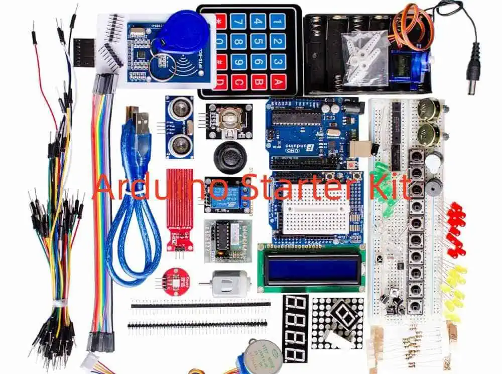
Device Hardware

In internet of Things, the devices are the physical things that make up the “things.” They serve as a bridge between the physical and digital worlds, and based on whatever function they are needed to carry out within the given IoT deployment, they might take various shapes, sizes, and technological complexity levels.

Almost any material object, including animate ones such as humans or other animals, can be made together into a specific connected device through the inclusion of the required instrumentation (by introducing actuators or sensors along with all the necessary software) in measuring and collecting the required data. This includes microscopic devices or large construction equipment.

 Of course, actuators, sensors, as well as other telemetry equipment can also function as independent smart devices. The exact IoT application and requirements of the hardware are the only restriction that can be experienced here (size, deployment ease as well as management, useful lifetime, reliability, cost-effectiveness).

Device Software

The ‘smartness’ of connected gadgets is actually due to their device software. The implementation of connectivity with its cloud, coupled with data collection, device integration, and real-time analysis of data within are all handled by software.

Additionally, it is a device software which supports application level features for individuals to communicate with its IoT system as well as visualize data.

Communications

Once the software and hardware for the device are in place, another layer must be added to give smart objects ways to communicate with the remainder of an IoT ecosystem. It is important to think of communications mechanisms as a standalone system despite the fact that they are closely related to the software and hardware of devices. Physical connectivity options (LAN, satellite, cellular) and particular protocols utilized in various IoT contexts are both included in the communication layer (Thread, ZigBee, MQTT, Z-Wave, LwM2M). One key components in building all the IoT technology stacks is selecting the appropriate communications solution.

The technology selected will influence how data is transferred to and received out from Cloud, as well as how these devices are maintained and interact with other devices. Later in this article, we shall go into specifics of a few modern communications technologies for the sake of the current essay.

Platform

As was already established, the gadget can “feel” what is happening around it, then it will transmit that information to these user over a particular communications channel because of the “smart” software and hardware installed. All of this data is collected, handled, processed, analyzed, and then presented in such a user-friendly manner on the IoT platform.

The capacity of such a system to analyze and derive value from the sections of data given by these devices through the communication layer, rather than just its data gathering and IoT management skills, is what makes it particularly valuable.

Once more, there are a lot of different IoT platforms available, and this choice will depend on the needs of the individual IoT project as well as criteria like architecture as well as the IoT technology stack, customization options, reliability, used protocols, hardware independence, security, as well as cost-effectiveness. Also it’s important to note that platforms could either be installed locally or be hosted in the cloud. A nice illustration of this type of platform is the Coiote IoT Device platform, which can be set up both locally and in the cloud.

IoT technology Stack Connectivity Options

The connectivity solutions that support IoT technologies are as many just like the potential real-world applications for them. Each communication solution may offer various service enablement possibilities while offering tradeoffs between the power consumption, bandwidth and range based on the requirements of a specific IoT Application.

For example, if you’re designing your smart home, then you might want to interface your heating controller and indoor temperature sensor with your phone so you will be able to remotely monitor these temperatures in every room as well as modify them as needed. The suggested remedy in this situation would be Thread, an IP-based networking protocol created specifically for different home automation environments.

Given the variety as well as multiplicity of the communication protocols and standards, it is reasonable to question the necessity of creating new technologies when there are already existing tried-and-true Internet protocols in use. This is due to the fact that current Internet protocols, including Transmission Control Protocol and Internet Protocol, frequently aren’t efficient enough but need too much power to function effectively in the growing applications of IoT technology. The primary alternative protocols for the internet specifically created for usage by IoT systems will be briefly discussed in this section.

The overview focuses on the most widely used Internet of Things radio technologies, split down by the radio-frequency range each of these solutions achieves: short-range, medium-range, and long-range WAN solutions.

Short-range Network Solutions for IoT

Monitoring IOT Devices

Bluetooth

Given its extensive integration with phones, Bluetooth is regarded as the go-to short-range communication technology, especially for the market future of wearable electronics, including wireless headphones and geolocation sensors.

Bluetooth Low-Energy protocol uses a negligibly small amount of the device’s power and was created with cost efficiency and minimal power usage in mind. The trade-off is that BLE might not be the best option when exchanging larger volumes of data often.

RFID

Radio-frequency identification, one of the earliest IoT applications originally developed, provides positioning solutions to serve IoT applications, particularly in the logistics and management of the supply chain, which need the capability of establishing the position of the object inside buildings.

RFID technology obviously has a bright future beyond basic localization services, including potential uses including patient tracking in hospitals, increased healthcare productivity, and real-time product location data in order to reduce out-of-stock situations present in retail establishments.

Wifi

It was built on the foundation of IEEE 802.11, and it is still the most popular and well-known wireless communications. The IoT industry’s capacity to use it widely is mostly constrained by its higher-than-average power consumption, which is a byproduct of the necessity to maintain high signal strength and quick data transfer for improved connectivity and reliability.

Although WiFi is a significant technology for the advancement of the Internet of Things, it also must be managed as well as utilized in marketing in order to generate revenue to users and service providers.

Linkify is a great illustration of a unique platform for WiFi management that provides the value-added services enabling open access points for WiFi. Linkify, one of the cutting-edge technologies of the AVSystem, offers nearly infinite marketing as well as customization possibilities for guest WiFi.

ZIGBEE

The most common industries in which this well-liked wireless mesh standard is used are the machine sector, home electronics, and systems for traffic management. Zigbee, which is based just on IEEE 802.15.4 standard, provides low data transfer rates, low energy consumption, security, and dependability.

THREAD

Thread, which was created expressly for home products, uses IPv6 connection to let connected devices talk to one another, have access to cloud services, or engage with users through the Thread mobile application.

Given the saturation of the market, Thread’s critics have argued that adding another wireless protocol for communication will only further fracture its IoT technology stacks.

Solutions for Long Range WAN (Wide Area Network)

Arduino IOT

NB-IOT

Narrowband IoT can be described as a new radio technology that is a derivative of 3GPP technologies, which is now in use. It guarantees exceptionally low consumption of power (A decade of operation of the battery power) and connection with a signal strength that is roughly 23 dB less than that of 2G. Additionally, it makes use of current network infrastructure, guaranteeing both assured signal quality and global coverage for LTE networks. This aspect often makes it possible to use NB-IoT in place of technologies like Sigfox or LoRa that require the creation of different local networks.

LTE-CAT M1

M2M and IoT devices having medium requirements for the data rate can be connected using the low-power wide-area standard for connection known as LTE-Cat M1. Relative to other cellular technologies like LTE-Cat 1, 2G, or 3G, it has extended battery lifecycles as well as provides improved in-building range.

Because CAT M1 is applicable to the present LTE network, carriers do not need to invest in the new infrastructure before they can use it. LTE Cat M1 is superior to the NB-IoT for the mobile applications since it handles hand-over between the cell sites more better and is also more comparable to the high-speed LTE.

LORAWAN

This is known as the long-range low power Wide-Area Networking that supports massive networks containing millions of phones and devices and is designed for low energy consumption. In order to provide low-cost, and ensure bi-directional communication in M2M, IoT, smart city, as well as industrial applications, this LoRaWAN is built with wide-area network applications in mind.

SIGFOX

The idea underlying Sigfox is offering an efficient connection option for M2M applications of low power that need low amounts of transfer of data but can’t use cellular service since it costs too much and uses too much power and WiFi range seems too short for them. UNB is a technology used by Sigfox, allowing it to be able to handle slow data transfer rates between 10 to about 1,000 bits each second.

It offers a stand-by time for a battery of 2.5Ah of 20 years while using approximately 100 times lesser energy than cellular communication systems.

Sigfox confirms that it is suitable for different M2M applications, which includes intelligent meters, smart street lighting, security devices, patient monitors as well as environmental sensors. It provides a reliable, energy-efficient, as well as scalable network that can support communication in-between millions of devices that are battery-operated over some several square kilometer areas. A rising number of Internet of Things (IoT) technological solutions, including Coiote, to name just one, currently use Sigfox.

What are Benefits and Drawbacks of the IoT Technology?

IoT has several benefits, some of which are listed below:

  • Better communication between the connected devices
  • The ability to obtain details from anywhere and at all times on all devices
  • The ability to transfer data packets across a unique and connected network thereby saving money and time
  • Ability to automate tasks enhancing the caliber of the services of a business as well as reduce the requirement for intervention of humans

The following are some drawbacks of IoT:

  • As the connected devices available increases and information is transferred more often between different devices, the risk that any hacker may steal sensitive data rises as well.
  • Enterprises may someday have to manage enormous numbers of different IoT devicesโ€”possibly millionsโ€”and it will be difficult to collect and manage this data from these devices.
  • It’s conceivable that every linked device would become corrupted whenever the system has a problem.
  • Since there is no global IoT interoperability standard, it is challenging for devices got from various manufacturers to connect devices with one another.

IoT Applications for Consumers and Businesses

The IoT technology has many practical uses, from consumer and business IoT through manufacturing as well as industrial IoT. Numerous industries, including the automotive, communication, and energy sectors, use IoT applications.

In consumer markets, for instance, smart houses with networked heating, lighting, electronic equipment as well as smart appliances can be operated remotely using smartphones and computers.

In order to make users’ life more comfortable and easier, wearable technologies with software and sensors may gather and analyze data of users. They can also send messages onto other technologies concerning the users. In order to improve first responders’ reaction times during different emergencies, wearable gadgets are also employed in public safety. Take for instance, they can provide efficient routes to the location as well as monitor the vital signs of firemen or construction workers at potentially fatal work sites.

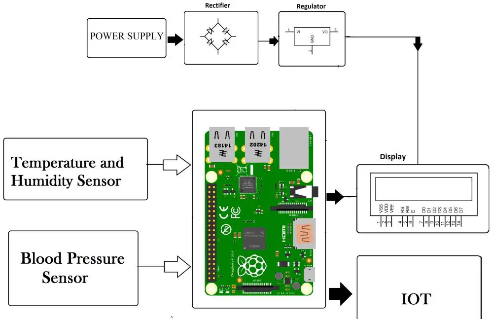
IoT in healthcare has several advantages, one of which is the capacity to track patients very closely by analyzing the data produced. IoT devices are frequently used in hospitals to carry out activities like managing the inventory of drugs and medical equipment.

Utilizing sensors that determine the number of inhabitants inside a room, smart buildings for example, can lower energy expenditures. Automatic temperature adjustments can be made, such as turning on air conditioners if sensor senses that there’s a full conference room or reducing the heat when everyone has left the workplace.

IoT Privacy and Security Issues

IoT uses data points (billions) to connect billions of different devices onto the internet, and all must be protected. Also, IoT privacy and IoT security are identified as important problems due to the larger attack surface.

Since IoT devices remain interconnected, a hacker only needs to take advantage of one weakness to change all the entire data and make it useless. Devices made by manufacturers who don’t update them frequently or never leave them open to hackers.

Additionally, users of linked devices are frequently prompted to provide personal data such as names, addresses, ages, phone numbers, as well as social network accounts. This data is useful to hackers.

The IoT technology is also threatened by privacy issues, which are a top priority for the IoT users. manufacturers and distributors of customer IoT devices might utilize those gadgets to collect and market the personal information of customers.

Conclusion

Given the rapid pace of the IoT development as well as the fact that it has already established a comfortable presence in different homes, workplaces, public spaces, and manufacturing facilities, it appears that the clichรฉd IoT adage “anything that could be connected would be connected” is rapidly approaching becoming our everyday reality. So, rather than asking when this would happen, the actual question ought to be ways in connecting everything in a way that maximizes efficiency while maintaining essential elements like cost-effectiveness and security. IoT is useful for data processing, data encryption, wireless network, smart home devices, health monitoring devices, and more.