Protoboard vs Breadboard: What are the Differences and Similarities

Protoboard vs Breadboard

In the Printed Circuit Board (PCB) market, some terms can be confusing. Two of such terms are protoboard vs breadboard. For some, they are one and the same, but to others, there are also differences between the two.

This article explains the differences and the similarities between the protoboard and the breadboard.

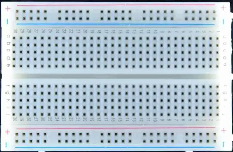
What is a Breadboard?

Letโ€™s go back in time. The term, โ€œbreadboard,โ€ was originally used to refer to the board upon which bread is laid for cutting. In the modern electronics industry, the meaning has been expounded to mean the construction base or platforms for making prototypes or earliest designs of electronics.

What is Protoboard?

The full name is prototyping board. As the name suggests, it is the board upon which the prototypes of electronic devices are made or built.

What is the Difference between Prototyping Board vs. Breadboard?

Solderable Breadboard

In electronic circuits, the difference between protoboard vs breadboard is not always easy to decide. According to Wikipedia, the breadboard is also known as the protoboard and solderless board. As such, it infers that protoboard is the same as a breadboard and vice-versa.

When to Use Breadboards or Protoboards

From the definitions, you can see that both the protoboards and the breadboards refer to almost the same thing. However, they can serve a single purpose โ€“ enabling the making of earliest designs of PCBs or electronic circuits.

Here are some of the instances of when you need to use the breadboard or protoboard:

Circuit Building/Development

The primary function of the breadboard is to enable the prototyping or making of the earliest designs of Printed Circuit Boards (PCBs).

The beauty of the process is that you can do all these without necessarily soldering. You will learn more about how this works in this article.

Circuit Board Design Learning

The use of protoboards or breadboards also paves the way for the circuit board learning process to be easier. Due to the reusability, solderless process and zero track destruction; it makes a good learning tool for PCB enthusiasts.

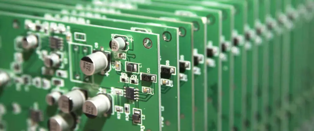
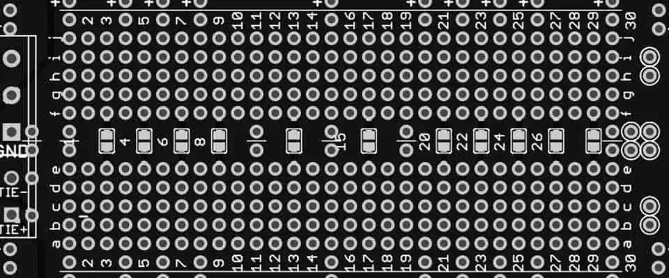
What Makes up the Protoboard?

An ideal breadboard or protoboard is made up of some elements. Understanding how they all stack-up and work is a major step to understanding how the different parts combine to boost the boardโ€™s function.

Plastic Socket

The first thing you will notice is the perforated block of plastics that make up the solderless board. It is common for the plastic socket to comprise of the following:

  • Several alloy spring clips are located underneath the perforations. These clips can be derived from either the tin-plated phosphor bronze or the nickel silver.
  • The alloy spring clips also serve as the tie points, i.e., the contact points for the fabrication.

Interconnecting Wires

Wires used for interconnection are often used to fill-up the free holes located at the centerline of the block. They are being inserted to straddle the block.

Metal Strips

The metal strips are used to make a pin-to-pin connection on the protoboard. Depending on the specifics of your fabrication, the boards can be clipped together as a way of forming a bigger protoboard/breadboard.

Bus Strips

This is the third type of strip used in a breadboard. The function of the bus strips is to provide power for the electronic components mounted on the protoboard.

The compositions of the bus strips include:

  • One column delegated to serve as the supply voltage.
  • Another column used as the ground for the board.

Sometimes, there are disparities as to how these compositions are made. For example, you could find some bus strips with a red marking denoting the supply voltage and the column intended for the ground marked either in black or blue.

Jump Wires

Breadboards also use a variety of jump wires. Popular options are manually-manufactured and ready-to-use variants.

While you can find the manually-manufactured variant difficult to use with larger circuits, the ready-to-use variant offers more versatilities.

Types of Protoboard

FULL PCB MANUFACTURING Quote

You will find two major types of protoboards. These are the soldered and the solderless. While the former can be soldered, the latter doesnโ€™t necessarily need to.

Let us see how they compare:

Soldered Breadboards

This type of breadboard or protoboard requires the use of solder to fit each of the leads or jumper wires into the designated holes.

Solderless Protoboards

Since they donโ€™t rely on the use of solders, the solderless protoboards can be easier to use. In place of the solders, the boards use a metal clip attached to the hole for capturing either the jumper wires or leads when any of those are inserted.

Differences between the Soldered and Solderless Breadboards

The major differences are:

  • Soldered protoboards use solder, while the solderless doesnโ€™t.
  • In terms of performance, the soldered breadboards are high-performing, due to the permanent capture of the leads.
  • In terms of versatility, you will find the solderless protoboards a better option. This is because of the reusability โ€“ a feature the soldered breadboards donโ€™t support.

Why Do We Need Breadboards?

You need to use a breadboard if you want to reduce the risks of designing circuit boards that end up having one design issue or the other.

You also need to use one of these boards to meet the following needs:

1. Temporal Circuit Design

You need the breadboard to make a temporal or prototype design of your electronic circuit.

2. Faster Prototyping Process

You will find out that, in some cases, you may end up processing the electronic circuitโ€™s prototypes faster with the use of breadboards.

It is obtainable due to the zero use or demand for advanced tools, such as a CAD software. Besides, it is more of a hands-on process.

In extension, you will save costs in terms of not manufacturing several PCBs at once. You also save costs due to the use of manualized processes, other than paying for a CAD software or any other advanced/automated prototyping tool.

3. Adaptive Circuit Design

A Printed Circuit Board (PCB) is said to have an adaptive design if it supports the detection of issues, the real-time implementations of changes and making repairs, where necessary.

Since the entire circuitry is open, you can make these changes almost at the same time.

4. Flexible PCB Probing and Testing

Detecting and fixing the issues relating to how a circuit board is designed is also another reason for using the breadboard.

The outlined process allows you to have a full glance of all the components and to make an unrestricted probing of each of them.

Moving from a Breadboard to Protoboard

Do you know that the major difference between a breadboard and a protoboard is not the name differences? It is indeed in how they function. Although they are used as a sort of โ€œbuilding blockโ€ for the first set of electronic circuits, they can sometimes be independent of each other.

You can move from a breadboard to a protoboard when it is time to make a detailed prototyping of the board.

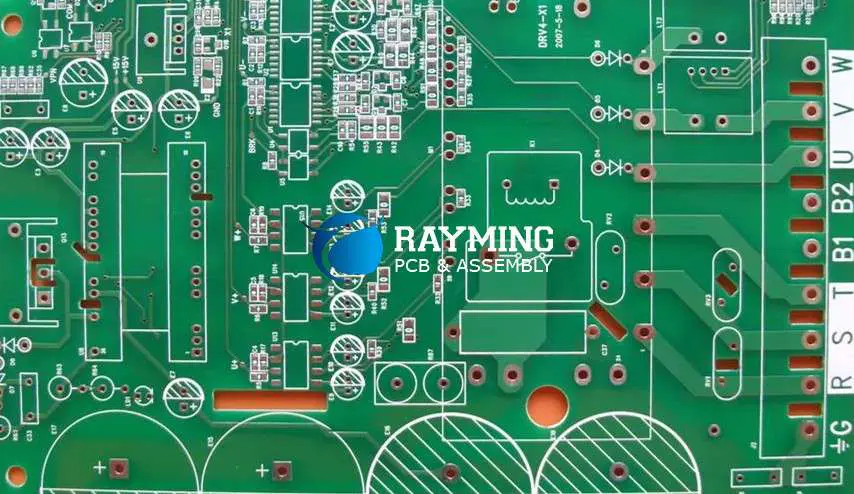
Here are some of the reasons why a protoboard (also called a prototype PCB layout) is better than the breadboard:

1. Connection Solidity

The connections and interconnections on a prototype PCB layout are more solid. This is because of the permanent capture of the leads. This way, you are assured of the fact that the leads wouldnโ€™t slip out during the prototyping process.

2. Improved Signal Integrity

While trying to keep the boardโ€™s performance optimal, you also want to be sure of the signalโ€™s integrity. The signal is greatly improved when using the protoboard, thanks to the absence of higher parasitic capacitance and inductance โ€“ a feature common with the solderless (breadboard) board design.

3. Copper Durability

In place of the jumper wires and metal connections used in the breadboard; copper is used for the protoboard.

4. Custom Prototype PCB Design

By default, the breadboard has a definite size, which you are expected to use for the prototype. On the contrary, this limits you to work within the ambient of that real estate.

On the other hand, the protoboard offers the flexibility that allows you to create custom PCB prototype designs and sizes.

5. Voltage and Current-Carrying Capacities

The capacities of the current and the voltages are higher in the protoboard. This is possible because of the adjustability of the metal area fills or power traces when designing for optimum width.

6. Flexible Component Usage

Protoboards also make the temporal electronic circuit design fun due to the flexible support for component usage.

Ideally, you wouldnโ€™t be restricted to using one type of component (usually, the through-hole components).

This time, you can choose between the through-hole and Surface Mount Devices (SMDs) for the prototyping.

5. Circuit Board Replication

The Printed Circuit Board (PCB) needs to be replicated in due time. For example, you may want to make variations of the prototype. It is a herculean task to do with the use of breadboards.

This is why you need to use an advanced and almost automated process, as the protoboard presents. This allows for the faster replication of the prototyped boards.

6. Cost Implementations

The manualized or breadboard process of prototyping a board is quite expensive and not time-critical. You spend a lot of time making a temporal design of one of the boards, and at the same time, would spend more to make copies of it.

The reversal is the case with the automated and scalable architecture of the prototype PCB layout board.

Limitations, Downsides and Disadvantages to Breadboards

Protoboard for pcb
Protoboard for pcb

The solderless (breadboard) approach to making circuit board prototypes comes with a lot of disadvantages.

1. Risks for Complex Electronic Circuits

You may not encounter major problems when working on less-complex circuits. But when working on the complex electronic circuits; the challenges triple.

Here are some of the considerations:

  • The large amounts of wiring used in the breadboards can make the management of complex circuits almost impossible.
  • The risks of contact resistance development are higher.
  • Signal integrity and overall reliability of the system/circuit is at the mercy of the flexible connection methods. You are just one plugging and unplugging away from distorting the entire process.

2. Component Preferences

Solderless boards or breadboards work best with the through-hole electronic circuits. The preference for this is largely attributed to the challenges experienced with using components with wider spacings, of more than 2.54mm. This is the reason why the Surface Mount Devices (SMDs) are not a popular choice for this process.

The inability of the electronic components to match the specifics of the Dual In-Line layout is also an issue. In this case, it is almost impossible to provide the accurate electrical conductivity.

3. Limited Operations

Do not expect the solderless boards (breadboards) to function up to a certain limit. This is because of the limited operations โ€“ a derivative of the high inductance and larger parasitic capacitance.

The following are examples of the limitations:

  • The operations of the breadboard are limited to certain low frequencies. These can be as low as less than 10 MHz
  • Limited voltage and current-carrying capacities.
  • โ€œThe relatively high and not very reproductible contact resistanceโ€ can also pose a challenge for some Direct Current (DC) and low-frequency circuit boards.

Conclusion: How Do Breadboards Compare to PCBs?

The main purpose of breadboard is to simplify the process of making temporal designs of electronic circuits. These designs allow for the early-stage testing, analysis and fixture of the different issues before the mass production begins.

When compared to the Printed Circuit Board (PCB), prototypes help to save both money and time. You can always detect and fix the issues in good time, as compared to going back to the โ€œdrawing boardโ€ to map-out how to fix those issues after the board has been produced in the quantities.

Besides, using either breadboards or protoboards helps you to get acquainted with what it takes to make circuit boards. You will find out the technicalities, be able to master the design concept and create better electronic circuits.

Rayming Technology helps you note the design issues, and test the circuits to be sure they are in good working conditions. With an extensive experience and industry-leading equipment, we will make prototypes of your circuits and ensure that everything works as they ought to.

What is Micro Sectioning on a PCB (Microsection)?

microsection PCB

Some people know about sectioning on PCBs. However, this is not what it takes to be a PCB nerd at all. Do you know about micro-sectioning on a PCB? Not yet? Well, feel lucky since we are going to explain micro-sectioning right in this post for your today!

You define micro-sectioning as a much finer process than sectioning that takes place on congested and tight areas of PCBs. No, we are not going to let you go with this simple definition. There is more to micro-sectioning, and it needs your attention for your future projects as well. 

YouTube video

Role of Micro Sectioning on a PCB

The purpose of micro-sectioning is to exclude some layers and components of complex PCBs so that you can detect the faults in the layout, PCB parts, and their performance. Now these layers can be totally damaged as well. If you go for micrometer scale sectioning, you will be able to cover all the important aspects of solder joints and their robustness on PCBs, material composition, and, yes, plating thickness is also on the list. 

Uses of Micro Sectioning on a PCB

PCB microsection
PCB microsection

 Have you ever been interested in surgery? Or might you get a surgeon friend that cuts open humans in an operation theater? Well, consider micro-sectioning as the surgery of the PCBs. You cut open a PCB, perform micro-sectioning and see where the faults lie. Pretty similar to a normal human surgery, but letโ€™s not go deeper into this analogy. There are some small steps that contribute to the success rate of this process. These are:

  • Using a raw functional material of PCBs
  • Perform build verification on the PCBs
  • See if the width of hole-wall plating is suitable or not
  • Whether all the conductors are of appropriate thickness or not
  • Register all the paddings on the inside and outside of PCBs
  • Develop connections between the PCB layers
  • The surface finish of PCBs has a correct thickness, or not
  • How thick is the solder mask 

ยท It’s time that we see how the PCB producers perform micro-sectioning at different intervals of PCB production. These include:

  • Check the size and quality of the holes
  • See if the registration is proper or not after drilling
  • Verify the width of the wrapโ€™s thickness and the barrelโ€™s thickness after plating
  • Check consistency, plating, roster, and problems that occur during the last stage, which is the quality assessment

Creating the Micro Sectioning on a PCB

YouTube video

Now your geeky brain must be wondering how PCB producers even create micro-section. There is no rocket science in it. Producers rely on special through-hole coupons for this purpose. Before doing this, they need to prepare the cross-sectional area of PCBs where they are going to perform the through-hole method. A process called automated coupon extraction is viable for CNC routing that assists in the extraction of the coupon. Other than this, there are some important factors that you need to know for the process:

  • Precision router-cutter machines are important for the determination of PCB cross-sectional area through buried and blind holes.
  • Also, the functions of these machines change as per their use for vendor qualification, failure analysis, conformance, and lot verification.
  • Once you choose your purpose, you grab the coupon and cut a small piece of it for the sake of sampling.
  • Now dip it in the resin or a soft acrylic if you have
  • Wait for it, and it will harden itself to form a hockey puck-like structure.
  • After this, you will crush this hockey puck structure and change it into a fine flat surface.
  • Polish the surface, and etch it as well if there is a need.
  • In the end, use a microscope to visualize and analyze the PCB.

Analyzing the Micro Sectioning on a PCB

FULL PCB MANUFACTURING Quote

There are different steps that you need to perform when analyzing your micro-section:

  1. Build Checking: It means you are verifying the layers of complex PCBs through the process of micro-sectioning. It includes checking the width of cores, foils, prepregs, and also the connection between the solder joints. Not just this, build checking helps you verify if there are any cracks, thermal stress, delamination, gaps, and blistering on the layers. 
  2. Wall Plating Thickness in PTHThe producers love to combine the through-hole method with micro-sectioning when analyzing. It helps you go deeper into the verification and quality check of PCBs. They use a coupon on every production panel they rely on. Six measurements are important to take, three per side of the hole. When you calculate the average of these six readings, you get the wall plating thickness. 
  3. The thickness of Conductors: You already know that we don’t plate the internal layers of PCBs at all. It means you can use micro-sectioning to check the width of internal layers. Sometimes cleaning just removes some of the copper from the layers. However, you can still find some traces of copper left on the foils. It will help you determine the thickness. 
  4. Hole Registration: When you analyze the micro-section by using a microscope, the internal padding is quite visible. Besides, you can also check the tolerance as well. A special coupon is important for this purpose, and you use it on all the panels. It helps you identify the position of the drilled holes in accordance with the layers. 
  5. The connection between Layers: The PTH should be with a strong connection with the internal copper layers. When you perform micro-section analysis, it enables you to detect problems like insufficient hole-wall cleaning, which can lead to faulty drilling and weak connections. 
  6. Surface Finish: You can even detect the surface finish of PCBs through micro-sectioning. Surface finish like lead-free HAL and hot air leveling support micro-sectioning. However, you can only measure the Nickelโ€™s thickness through this if you want to determine for ENIG. Use X-rays for this purpose. 
  7. Solder Mask: Sometimes, you need to measure the width of the solder mask, and micro sectioning just makes it happen for you. The standard thickness of the solder mask is always 8 micrometers. 

Micro Sectioning on a PCB for Traceability

If you have ever observed a coupon, there are some fine markings present on it. These markings help you identify the machine that produced it in the past. Now, this helps you in separating healthy PCBs from sick ones. Not just it, you can even reduce the chances of possible failures of PCBs through traceability. 

Identifying Failure with Micro Sectioning on a PCB Analysis

So the question is, how do you stop your PCBs from failing through micro-section analysis? Weโ€™ll see that in just a bit! 

  • If your PCBs have faults and defects like improper solder mask thickness, poor etching, or defective registration, micro-sectioning can help you with it.
  • The areas which are uneasy to reach out to, like pads, solder masks, and micro-sectioning, open a doorway for you to easily access these areas for analysis.
  • Once you collect the data given by micro-section analysis, you can later use the same data for improving the PCBs
  • You can rely on micro-sectioning for the failure analysis of PCBs as well when the internal failures keep hidden from the technicians.

Challenges of Micro Sectioning on a PCB

Letโ€™s talk about the hurdles that you might face during micro-sectioning. Wait, did you think it was a smooth process? No, there are still some difficulties that you should take into your account. 

  • The equipment and the materials used for producing a PCB can complicate micro-sectioning since these materials are unlike in hardness, and the equipment might be challenging to handle for the technicians.
  • Sometimes problems with drilling can also occur.
  • The positioning of the spot must be in the boundary of 10% of PCB, which leaves no margin of negligence at all. 
  • In some cases, micro-sectioning can need you to use expensive equipment as per the complexity of your PCBs which can disturb your budget.

Additional PCB Testingโ€™s for Micro Sectioning on a PCB

Micro Sectioning on component

 Other than micro-sectioning, functional PCB testing also plays its role in ensuring the quality of PCBs. There are more tests that include: 

  • Using X-rays to completely visualize the internal area of PCBs
  • Test the PCBs for contamination that might lead to degradation and other problems like metallization.
  • Check the frequency of the board to prevent breakdowns.
  • Peel testing to determine how robust the laminate of PCBs
  • Testing the solder float to check the thermal stress each hole can endure
  • Flying probe testing is for checking the capacitance, inductance, and resistance issues of the PCBs
  • Automated optical inspection of PCBs uses the latest 3D cameras to take pictures of PCBs and analyze them from their photographs.
  • Burn-in testing is a rigorous procedure that you need to perform in the beginning; however, it can also harm the sensitive PCB parts.

Wrapping It Up

The bottom line is that micro-sectioning is becoming more important than ever since the PCBs are getting smaller for miniaturization. Since the process is crucial for quality checks, producers are training their employees for micro-sectioning as well. 

You also get a chance to diagnose the pain point of your PCBs through micro-sectioning. So, if you are facing problems like improper solder thickness, technical issues like lamination faults, and frequency changes, your PCB is in dire need of micro-sectioning. 

Hopefully, this discussion was helpful for you in terms of understanding micro-sectioning. We will see you in the next post with something more intriguing from the field of PCBs. 

What is BGA Via in Pad ?

bga via in pad

Have you been considering a PCB design with via-in-pad? Via-in-pad design is becoming increasingly popular, and if youโ€™re not familiar with the idea of vias on BGA pads, it may be in your best interests to explore this new printed circuit board design option that seems to be growing in popularity.

YouTube video

WHAT IS A VIA-IN-PAD?

A via-in-pad design, as the name indicates, is a printed circuit board design with the vias directly on the BGA pads. The main benefit of a via-in-pad design, also called VIP design, is that you reduceย the area needed for the vias, making it easier to manufacture miniaturized PCBs and dramatically minimizing the amount of board area you need for signal routing. With via holes connected directly to layers beneath the component, you can have signal routing without escaping the device footprint perimeter.

IS IT CONSIDERED BAD PRACTICE TO PUT VIAS ON BGA PADS?

Is this a good practice or a bad practice? Why isnโ€™t everybody doing it? In fact, many people are. It is becoming a common practice to put vias on BGA pads. Why donโ€™t all designers do it? The main reason is that if you put a via in pad, you have to fill it โ€” either with copper or a copper-covered non-conductive material. Non-conductive fill is most popular and more price competitive.  If you do not, the solder will flow away from the pad and you will not get a functional electrical connection.

Filling the vias is an extra step, and some designers may not want to incur the cost and lost time required to do it. Putting vias in pad also affects the drill diameter you will need. Nevertheless, there are many good reasons to opt for a via-in-pad design, which is why many PCB users do call for them, despite the slightly added cost and time commitment.

Next, what are the advantages and disadvantages of VIP vs. traditional via placement?

TRADITIONAL VIAS VS. VIP TYPES ADVANTAGES AND DISADVANTAGES

As mentioned, in a traditional via layout, you can simply apply solder mask to prevent the solder from drawing into the barrel of the via and creating electrical connection problems. But when you have via-in-pad, this will not work. You must completely fill the vias so there will be no air entrapment with resulting outgassing in the assembly phase. You also need a flat planar surface in order to attach fine-pitch BGAs as well as components effectively.

How can you fill these in-pad vias? After mechanically drilling and plating your in-pad vias, you must fill them with epoxy. Alternatively, you can laser-ablate your vias and fill them with copper. Which you choose to do will depend on your specific application and needs when it comes to your printed circuit boards as well as the size of the via. The main issue when deciding your process will be pad diameter. You need to make sure the pad size is large enough for the via diameter while still being able to accommodate manufacturing tolerances and meet the minimum IPC Class 2 or 3 annular ring requirement.

The VIP advantage is that once you effectively place the vias in-pad, you will enjoy some incredible space savings, and this can not only increase your efficiency but may also be required for certain modern applications. If you have a revolutionary application that necessitates space flexibility, VIP can be the ideal choice and may, in fact, be the only choice.

The advantages of via in pad

Via in PCB

There are a lot of advantages of via in pad PCB. First of all, Itโ€™s good for increasing density, using finer pitch packages, as well as lessening inductance. Whatโ€™s more, in the process of via in pad, a via is directly placed below the contact pads of the device, which can achieve greater part density and superior routing. So it can save a great quantity PCB spaces with via in pad for PCB designer.

Compared with blind vias and buried vias, there are many advantages for via in pad as follows:

  • Apply to fine pitch BGA;
  • Lead to higher density PCBs and promote space saving;
  • Improve thermal dissipation;
  • Provide a flat and coplanar surface with component attachment;
  • Lower inductance due to no dog-bone pads with traces;
  • Increase voltage capability of the via;

However, you need to confirm that your PCB manufacturer is well-equipped to fabricate your PCBs because it may cost more. If you are not able to place via in pad, putting directly and using more than one can assist in decreasing inductance.

When should I use via in pad?

It will lead to design rule check errors because of trace width, annular ring, as well as size limitations while trying to route and escape component packages with sub 0.5mm pitch with traditional routing methods. For the small pitch components, only to route them with capped via in pad can it make the circuit board routing to be as compact as possible.

And it can simplify routing for complex BGA and LGA packages as well with capped via in pad. And the components like bypass capacitors to be placed as close as possible with minimizing the surface routing so that minimizing parasitic inductance. In addition, the paths to power and grounds planes are short, which will be good for minimizing EMF emissions of high frequency designs.

Vias in thermal pads also can play an effect on heat management. In general, high power surface mount parts have a thermal pad that mounts to the circuit board. So youโ€™d better drop vias through the board to the other side of PCB to increase the copper area for heat release.

Via in pad application for SMD pad

1. Plug the via by resin and plated it flat by copper

It is compliant with small BGA via in pad;

First of all, the process is filling the via hole with a conductive or non-conductive material, and then plating the via on the surface, which provide a smooth flat for solderable surface;

There are used in via in pad designs where it can mount the component over the via, or extend the solder joint to the via connection.

2. Microvias and via in pad plated over

A microvia is a hole with a diameter of less than 0.15mm based on IPC. It can be a through via hole ( related to a aspect ratio ), however, in normal the microvia is regarded as blind vias between 2 layers;

There are a majority of drilling the microvias with laser but some PCB manufacturers are also drilling them with a mechanical drill bit, which is slower, however the holes have a clean and nice cut;

The microvia cooper fill process is an electrochemical deposition process used for the multilayer PCB fabrication process, it also known as capped vias;

Although the process is complicated, it can fabricate HDI PCB that most PCB manufacturers will get the copper filling of microvias.

3. Plug the via by solder mask

Itโ€™s free and compliant with big solder SMD pads;

The standardized LPI solder mask process can not form the fill vias without the risk of exposed copper in the hole barrel. In general, it can deposit UV or thermally curable epoxy solder mask into the holes to plug them after using the second screen print;

It is known as via plugging. Via plugging is used to plug via holes with a solerrsist material so that protect air from leaking as testing the boards, or prevent the components near the board surface from shorting.

Via in pad PCB

FULL PCB MANUFACTURING Quote

In PCB design, via is a pad with a small plated hole in a printed circuit board which are used for a connection between copper tracks on a various layers of a board. There is a via known as micro vias, which have apparent blind vias only on a single surface for high density multilayer PCB or invisible buried vias on either of the surface. Whatโ€™s more, there is a new challenge after bringing in and being widely used the high density pin out parts, as well as the need for small dimension PCB. So the better solution to meet the kind of challenges is using the latest but popular PCB manufacturing technology called โ€œ via in padโ€.

It needs to quickly use via in pad in the current PCB design due to the constantly reducing pitch of part footprints, as well as the need for miniaturizing PCB form factor. Whatโ€™s more, it can achieve signal routing in as little an area of the PCB layout as possible, in most instances, even avoiding escaping the perimeter of the device footprint.

Via in pads is mostly useful in high speed designs as they reduce trace length and consequently inductance. Youโ€™d better check whether your PCB manufacturer is well equipped to fabricate your board or not, because it may spend more money on it. However, if you canโ€™t place via in pad, directly putting and using over one to decrease inductance.

A Beginner’s Guide to DSBGA (Die-Size Ball Grid Array)

DSBGA

It is just another name for wafer-level chip scale packaging. Now don’t let the name of this process fool you. It’s not that hard to learn about. After reading this post, you will have sufficient knowledge about DSBGA so that you can educate others about it as well. 

 So letโ€™s get this straight. DSBGA is different from other forms of packaging because you do not separate it from the wafer at all. There is a fine layer of copper that combines the silicon connections and solder material. You keep the die of silicon smaller, which sets it apart from other types of packaging. 

To name one of its crucial applications, it will be using it when you do not have enough space. It is useful when you are considering miniaturization. It normally happens when you are producing mobile phones and smart wearables like health and fitness devices and trackers. 

Introduction

So this flip chip method is not a new one. Instead, it has been involved in common applications for many years. Formerly, producers would use it for the process of miniaturization.

 The archaic producers would always rely on smaller dies and would also reduce the number of connections of the semiconductors. The process included bumps made from metal alloys that offered strong bonding with the substrate. 

The SMT just enhanced the results given out by this process. As time passed, industry leaders and decision-makers gathered to educate the semiconductor sector to keep up with the latest technologies and new trends.

 So that they could be able to invent new solutions that have the potential to solve the problems of semiconductor production, since this was the key focus area of the stakeholders, it gave birth to a new technique that was useable for every producer. 

The evolution in miniaturization ended in keeping the die size equal to the package itself. Consider DSBGA as an alignment of metal balls that are beneath the package. On the other hand, you place the die with the substrate. 

Now it will allow smooth redistribution of the connections of the die with the pads. It is what we need to focus on and make sure it happens as well. You can use a substrate of any shape since there is no thumb rule for it. 

Today, producers follow the standard of keeping the substrate and die sizes the same during the process. It is because it keeps the chances of failure and error near to none. Plus, it promises positive results for the final products at the same time.ย 

Applications of DSBGA (Die-Size Ball Grid Array)

BGA Reballing

The fields of telecommunication and media cannot survive without semiconductors, and we all know it. People now love portable devices that do not feel bulky in their hands. Such devices offer more dependability and are exceptional in their performance as well. 

Modern users are now expecting smaller variations of these devices. Since nobody likes to carry heavy and clumsy gadgets, this is something that producers need to scratch their heads for. 

Semiconductors have always proved to be beneficial in reducing the sizes of smart devices. Not only this, they maintain the quality and performance of portable devices as well. Thus, they support miniaturization and help you invent the most cherishable marvels of all time!

It seems like we are just praising the semiconductors here; letโ€™s quickly hop on to the actual discussion – the applications of semiconductors that are too common. You might not have considered them before reading this post!

  • Highly important for producing portable MP3 players 
  • Different types of memory cards need DSBGA elements for proper working
  • Some common types of digital cameras use DSBGA as well
  • Man-portable video games and gaming consoles all use DSBGA 

You must be surprised to know that different producers are now considering miniaturization for wireless headsets and many other bulky devices to meet the expectations of consumers. They are devising solutions to make this possible. 

For this, DSBGA seems to be a multipurpose asset on all counts. Array packaging is another method that is interesting to know about. You do not need to worry about any type of lead frame for this packaging.ย 

Just use the same die for the flip-chip method, and you are good to go. It helps with more electrical density, which eventually boosts the electrical performance of the devices. Now you see how one small component can deliver you great results. 

Itโ€™s time that we discuss the doโ€™s and donโ€™ts of DSBGA in detail! So letโ€™s not keep you waiting!ย 

Assembly Process of DSBGA (Die-Size Ball Grid Array)

FULL PCB MANUFACTURING Quote

Die size (DSBGA) array packaging is undoubtedly a fruitful method that supports the production of many devices. 

Besides, the flip-chip method has also been successful in transforming less efficient devices into something that consumers can avail of in the longer run. Remember the DSBGA uses uncovered dies? 

So when you are using this type of die, there is a sure impact on the process as well. It means you need to be extra careful and concerned when using uncased dies.

 In this section, we are going to crack this code for you so that you wonโ€™t mess up anything when working with such a die. Ready to dive in? Letโ€™s start with it!

  • Never proceed with the process without encapsulating the uncased die because it can cause damage in the form of cracks.
  • Ignoring encapsulation can also disturb the siliconโ€™s expansion ability along with laminations and solder connections, which can complicate the process, thus lowering the success rate as well.
  • If you go for miniaturizing the die in the first place, it can save you from the aforementioned risks to a large extent.
  • Or else, you can rely on a special type of wire bonding called face-down wire bonding that is useful for packing silicone.
  • The best part about face-down wire bonding is that it regulates the performance and keeps it improving from time to time. 
  • The method is viable for reducing the package size as much as possible.
  • One thing that you need to take care of is that a license is important when you are performing this method. 

The End Note

The world will witness extreme miniaturization of smart devices and futuristic machinery in the forthcoming years. Owing to this fact, the producers would need to come together to reduce the size of silicon semiconductors even more than before.

It will make a pathway for the producers to enhance the circuit densities and maintain the quality at the same time. Hopefully, you have learned the importance of miniaturization through DSBGA from this post! We will see you in the next one, till then don’t let your fascination with the latest technology trends rest at all! 

Why Is XCZU4EV-2FBVB900E One of The Efficient System-On-Modules?

wholesale Xilinx FPGA

Do you want to know about XCZU4EV-2FBVB900E? This article is just for you. We’ll go over the technical specifications and other important details of this powerful FPGA. FPGAs are gaining popularity in the digital and electronic world due to their features. Let’s have a closer look at XCZU4EV-2FBVB900E to learn more about this.

 What Is XCZU4EV-2FBVB900E?

The XCZU4EV-2FBVB900E is a System-on-Module FPGA. Again its manufacture is by Xilinx. Xilinx is the name of quality in the field of logic devices.

 It belongs to the Zynq UltraScale+ MPSoC and provides high performance and low latency. This part number has been specifically designed for use in embedded systems. As a result, it provides high levels of computer power for applications. For example, machine learning, signal processing, and image processing, the list is long.

Here are some of the key features of the XCZU4EV-2FBVB900E:

  • It has Processing System Quad-core ARM Cortex-A53 with a dual-core Cortex.
  • This FPGA has Programmable Logic cells. 176K logic cells make it ideal for data processing
  • 6,600 Kb block RAM and 360 DSP slices are just the icings on the cake.
  • It has a great memory for data storage. 1GB DDR4 SDRAM (PS), 4GB DDR4 SDRAM (PL), 128 MB QSPI Flash, and 8GB eMMC Flash memory are great for data storage.
  • It can support many Interfaces. For example, PCIe Gen2 x4, Gigabit Ethernet, USB 3.0, SD/SDIO, and the list is long.
  • This FPGA Single 12V input with onboard power sequencing. So it has an efficient power management system. As a result, it is part of many delicate systems.             

Technical Specifications

xilinx kria board
xilinx kria board

Let’s take a closer look at some of the technical specifications of the XCZU4EV-2FBVB900E.

1. Exceptional Processing System

Processing systems are necessary for quick data processing. Asa result, they can show better results. The XCZU4EV-2FBVB900E employs a processing system that comprises a quad-core ARM Cortex-A53 with a dual-core Cortex-R5F Real-Time Processor and a Mali-400 MP2 GPU. It renders a notable degree of performance and versatility. As a result, it is an optimal option for an extensive array of embedded applications. Similarly, its exceptional performance makes it ideal for programmable Logic functions.

2. Programmable Logic Functions

The XCZU4EV-2FBVB900E features a large programmable logic section. As you know that it has 176K logic cells with 6,600 Kb block RAM. This provides a high degree of flexibility in system design. As a result, designers can implement custom algorithms and processing pipelines. Integrated circuits don’t work well for complex functions. Asa result, you can’t get desired results.

3. Exceptional Memory for Data Storage

Data storage is always an issue. That’s why designers always try to use FPGAs with extended Memory. The XCZU4EV-2FBVB900E includes a range of memory options, including 1GB DDR4 SDRAM for the processing system. Moreover, it has 4GB DDR4 SDRAM for the programmable Logic. 128 MB QSPI Flash. In addition, 8GB eMMC Flash is also there. As a result, it ensures that the processing unit has plenty of space for both program code and data storage. For example, if there is less RAM, then low data storage.

4. Interfaces And Their Connectivity

The XCZU4EV-2FBVB900E provides a range of interfaces. It includes PCIe Gen2 x4 and Gigabit Ethernet. Similarly, it includes USB 3.0, SD, and more. As a result, it allows easy integration with a wide range of peripherals and other system components.

 Alphanumeric Breakdown

 When you read XCZU4EV-2FBVB900E., then you may consider it an ordinary number. For your ease, we did it. The XCZU4EV-2FBVB900E is an alphanumeric code used to identify a specific System-on-Module (SOM) designed by Xilinx. Let’s see what these alphabets tell us.

Here’s a breakdown of the code and numbers

  • XCZ indicates the family of the SOM. It belongs to the Zynq UltraScale+ series. That’s why XCZ is the part number.
  • U4 indicates that it uses the Zynq UltraScale+ MPSoC with four processing cores. As a result, it offers high processing.
  • E indicates that it uses the Mali-400 MP2 GPU for graphics processing.
  • V indicates that it has a processing system with a dual-core Cortex-R5F Real-Time Processor.
  • 2F indicates that it has two GB of DDR4 SDRAM for the processing system.
  • BV indicates that it has eight GB of eMMC Flash for storage. That’s why it can store large data easily.
  • B indicates that it has a single 12V input for power.
  • 900 is the code for the package type of the SOM. Most package types are BGA. Thatโ€™s why it is compact packaging.

Now you have a better understanding of all the alphabet and numerals in this part number.

Frequently Asked Questions

FULL PCB MANUFACTURING Quote

What is the power input for the XCZU4EV-2FBVB900E?

The XCZU4EV-2FBVB900E has a single 12V input with onboard power sequencing. That’s why it has an efficient power management system. So it is part of many power-conservative devices.

 Is the XCZU4EV-2FBVB900E suitable for different applications?

Yes, of course, it is suitable for a wide range of applications. Different machine learning, signal processing, and image processing applications have this FPGA as an important part. That’s why Designers are trying to interrogate this FPGA with other systems so innovatively. As a result, these devices show better results.

From where can I get Xilinx’s at a suitable price?

You can buy it from an authorized dealer. Otherwise, there is fear of counterfeit products. Moreover, you can easily recognize this product to get the real one. The FPGA will have a pattern of small metal balls on the bottom side. Additionally, the packaging may also have a label. This label conation all the necessary information. In addition, it also conation the manufacturer’s logo and part number. That’s why it is easy to recognize. In addition, you can take help from the seller or dealer. So there is no need to worry about recognition.

Wrapping Up

XCZU4EV-2FBVB900E is an exceptional unit in terms of Memory and other specifications. Similarly, its processing speed is so exciting. That’s why designers and engineers like to use it in their projects. As a result, it is easy to explore many other applications and possibilities. It all depends upon your specific needs and requirements. Sky’s the limit as there are various options to employ FPGA. That’s why if you are looking for versatile FPGA, then you must go for it.

Why Should You Use XCZU6CG-L1FFVC900I?

Xilinx Artix 7

The XCZU6CG-L1FFVC900I is a powerful SoC device. It combines an Arm Cortex-A53 64-bit quad-core processor with programmable Logic. It is from Xilinx. The following content will help you to know more about this specific part number.

Let’s start with its specification and how it is unique from the rest of SoCs.

 Unique Specifications

This SoC is part of the prestigious Xilinx Zynq UltraScale and MPSoC family. Its specifications are following

  • SoC has 256k logic cells as building blocks.
  • It has 1,248 DSP slices for better processing.
  • SoC has an 1,872 Mb/s DDR4 SDRAM interface for better connectivity.
  • 20.8 Mb block RAM for better storage is a good deal.
  • It has 1,152 18×18 multipliers and 144 GTX transceivers:
  • It has ARM Cortex-A53 MPCore 64-bit quad-core processor and ARM Cortex-R5 real-time processor, up to 600 MHz.
  • ARM Maliโ„ข-400 MP2 graphics processing unit makes it ideal.
  • It has a Dual-core ARM Cortex-A53 32-bit microprocessor for system management.
  • It has USB 2.0 and USB 3.0 controllers.
  • SoC has Quad SPI and NAND flash controllers.
  • Break down the alphanumeric code.
  • Herein lies an explication of the alphanumeric constituents of the part number XCZU6CG-L1FFVC900I. These are not ordinary codes or numbers; actually, they have explicit meanings.
  • XC represents Xilinx, a prominent producer of FPGA and SoC devices.
  • ZU6 alludes to the precise model or type of the ingredient. Plausibly, it is a member of the Zynq UltraScale+, a family of FPGA and SoC devices assembled by Xilinx.
  • CG refers to the exact form factor or package of the component. It is a ubiquitous variety of surface-mount packaging utilized for a wide array of electronic components. It is plausible that it belongs to the ball grid array (BGA) package.
  • L1FF is a combination of letters and digits. It can signify the velocity grade or performance level of the element. That’s why It is plausible that component.
  • Support a high-performance device with a rapid processing capacity.
  • VC900I is a character string that acts as a kind of identification mark or serial number that distinguishes the specific component from other components with similar numbers.

This breakdown will help designers or hobbyists to have some basic information.

Why Should We Use This FPGA?

1. Amazing Security Features

The XCZU6CG-L1FFVC900I has a variety of security features. It has a TrustZone security subsystem, secure boot, and encrypted memory. The TrustZone security subsystem provides a secure environment for running sensitive applications.

Similarly, a secure boot ensures that the device boots securely. In addition, encrypted memory provides protection for sensitive data stored in memory. That’s why you don’t need to worry about data security. It is secure with this device. As a result, it performs better. For example, if there is a security breach, then nobody will like it.

2. Development Tools for Better Customer Design

Xilinx provides a variety of development tools for the XCZU6CG-L1FFVC900I.

 Vivado Design Suite, which provides a complete design environment for creating and testing custom designs for the FPGA. Xilinx also provides a variety of IP cores and reference designs. As a result, you can create defines easily and accelerate the design process.

3. High-Performance Architecture

The XCZU6CG-L1FFVC900I provides high-performance processing and acceleration capabilities. In addition, the dual-core ARM Cortex-A53 processor provides a high-performance, low-power solution for general-purpose processing tasks. This FPGA is part of a wide range of applications. S data processing and machine learning are examples.

The cortex processor operates at a clock speed of up to 1.5 GHz. The Cortex-A53 is a power-efficient processor and provides high performance in a compact size. That’s why it is ideal for use in embedded systems and other low-power applications. In addition, the processor can run Linux. Similarly, it also supports other operating systems so easily. That’s why it provides a familiar environment for software development.

4. Acceleration For Graphics

ARM Mali-400 MP2 GPU provides hardware acceleration for graphics processing tasks. As a result, The GPU can handle complicated tasks. For example, video decoding and encoding, image processing, and the list are long.

5. Rich Set of Peripherals

 The XCZU6CG-L1FFVC900I comes with a rich set of peripherals. This help to integrate with different system such as Ethernet, USB, PCIe, and more. Similarly, these peripherals enable various communication and connectivity features in your application.

The XCZU6CG-L1FFVC900I FPGA supports a variety of connectivity options. For example, it includes Gigabit Ethernet, USB 3.0, SATA, and PCIe. The Gigabit Ethernet interface supports high-speed connectivity to networks. In addition, USB 3.0 interface provides high-speed data transfer to exterior devices. The SATA interface provides support for storage devices. Similarly, the PCIe interface supports high-speed connectivity to other devices, to graphics cards.

6. Programmable Logic and Excellent Memory

One of the key features of the XCZU6CG-L1FFVC900I is its programmable Logic, which provides the ability to customize the device for specific applications. The programmable Logic is based on Xilinx’s UltraScale+ architecture, which provides high performance and low power consumption. The device features a good number of logic cells, making it one of the most powerful SoC devices available.

The XCZU6CG-L1FFVC900I has a variety of memory options. It includes a

Four GB DDR4 memory controllers, Similarly, It also has 512 MB of Quad-SPI flash memory and sixty-four KB of non-volatile memory. The DDR4 memory controller provides high-speed access to memory. That’s why it is ideal for use in high-performance applications.

7. Low-Power Design with Adjustable Voltage and Frequency

FULL PCB MANUFACTURING Quote

The XCZU6CG-L1FFVC900I is known for low power consumption. Moreover, it is critical for battery-powered or energy-efficient.

The XCZU6CG-L1FFVC900I has power efficiency with a variety of features. It reduces power consumption. These features include dynamic voltage and frequency scaling. That’s why it easy to adjusts the voltage and frequency of the process. As a result, it matches the workload and power gating. So it shuts down unused parts of the device to save power.

Wrapping Up

The XCZU6CG-L1FFVC900I is a powerful SoC. Moreover, it brings together a quad-core Arm Cortex-A53 processor and programmable Logic. It provides superior processing capabilities and multiple memory options. That’s why it stands as an ideal component for a range of applications, including embedded systems. In addition, its vast capabilities make it a remarkably versatile device. As a result, it is capable of dealing with a wide range of complex and challenging computational tasks.

What is the Essence of Thermal Relief in a PCB?

Thermal Relief PCB

Heat dissipation concerns are on an increase in recent years, following the clustering or closer placement of components on circuit boards. Due to the proximity of these parts, it has become increasingly difficult to dissipate or keep away heat or thermal energy within the board. Today, one can use thermal relief pads to conduct heat away from the components.

In this article, we define thermal relief PCB, explain the important and explain how you can maximize it for the best thermal management results.

Thermal Relief PCB Meaning

Thermal relief, also called thermal relief pad and thermal pad, refers to the dedicated pad that manages heat/thermal transport in a circuit board.

Thermal Relief PCB Footprint

The primary function of the pad is to provide โ€œreliefโ€ to the PCB, in terms of the heat conduction capabilities. For this purpose, let us look at some of the factors that go into making the footprint.

The Location

The thermal relief PCB pad is designed as a large area of metal, meant for enabling the soldering of the metal to either the circuit board or the device.

It is also possible to solder or attach the metal to other surfaces, such as heatsink and a bolt.

Thermal Relief PCB Connection

The pad is usually connected between the heatsink and the heat-generating components. This is done to facilitate the further conduction away of the heat coming from these parts. That way, other components wouldnโ€™t be exposed to the heat and the negative effects.

Also, the thermal relief pad is commonly used in the location where there is either an existing connection between the fan-out via or the component pin to the copper plane.

The Copper Pour Connection

The argument is on whether the thermal relief pad is to be connected to the copper pour or to the tracks. These tips will help you make the right thermal relief PCB connections:

  • The thermal relief pad can be connected to the copper pour via a thermal connection. The connection is enabled by the use of 3 to 4 traces of copper spokes to have the pad attached to the surrounding copper.
  • For the best results, it is best to connect the pad to a few narrow tracks. The reason is that a direct connection to the copper pour makes the padโ€™s soldering difficult.

PCB Thermal Relief Guidelines

Designers ought to follow certain steps and guidelines, as these help them optimize the thermal relief pad for the best results.

Here are the cardinal points of utilizing the pad in your circuit boardโ€™s layout:

Thru-Hole Component Pins

Also called the thru-hole pins; these are the pins, which have been drilled through the circuit board for soldering purposes. The major concerns for using the thermal relief PCB pad for these pins are:

Cold Solder Joint

There is a risk of having a cold solder joint created. It is a result of the inability of the thru-hole pins from getting enough heat for solderability purposes.

The reasons for the inability to create good solder joints include:

  • The tendency of having heat pulled away from the pin by a split plane or any other small metal area. The resultant effect is that the area serves as a heatsink and takes away the heat.
  • The cold solder joints are created in multilayered PCBs, whereby an excessive amount of heat is required to extend beyond the several square feet of metal.

Forceful Heat Application

FULL PCB MANUFACTURING Quote

There is another risk of having heat forcefully applied towards the melting of the solder. This happens as a result of trying to โ€œunsolderโ€ the solder that was directly soldered to the larger areas of the metal.

The outcome of doing this is that the surrounding components/parts and traces are exposed to damages.

Surface Mount Pins

These are pins used for Surface Mount Devices (SMDs). Possible issues tend to arise with the smaller, two-pinned SMT devices. These problems arise due to the directly soldering of one of the pins to the larger area of metal.

Here are some of the reasons why PCB designers would embed a surface mount pad in a metal fill:

  • The embedding might give the best of electrical performance, but it comes at the expense of pulling away heat from the thermal relief pad.
  • There is also a risk of having one side of the solder melting faster than the other, due to the imbalance of the metal between the pins.

The best way to tackle the imbalance of the metal is to use several traces to connect a surface mount thermal relief pad. This proves to be a better option, rather than having it embedded into the large area of metal.

Metal Routing

There is a tendency that the metal wouldnโ€™t be enough to enable the connection of the spokes to the surrounding copper. This happens due to the following reasons:

  • The automated process of using CAD systems for adding the thermal relief PCB pads to the pins often impacts the pad. This also leads to limited space for the spoke-to-copper connection.
  • Certain power traces with lower conducting levels of current are often routed with the narrower traces.

Vias

There might be no need to use the thermal relief PCB with the vias, especially the ones that connect to the larger area fills, power planes and ground planes. The reason is that they donโ€™t often have pins soldered into them.

The primary consideration for using the pad for the vias is due to the following reasons:

  • If you are using nets that conduct higher current levels.
  • If this is the case, use the thermal relief PCB pad because some short power traces might facilitate excessive heat conduction to the surface-mount pins.

What is the Purpose of Thermal Relief in PCB?

You need to know when to use thermal relief PCB for your circuit board. The following are some of the benefits:

  • The pads aid in the manufacturability of circuit boards.
  • You can use thermal relief PCB pads to provide a robust electrical connection from the pad to the plane.
  • It also aids in the preventing of excessive heat dissipation into the metal plane.

Conclusion

Thermal relief pads are used in PCBs to bolster the restriction of heat flow into the copper pour, keeps the heat confined in the pad required for PCB component mounting and improving the padโ€™s solderability.

American Manufacturing Vs. Chinese Manufacturing on Electronic Devices

Electronic Devices Manufacturing

The global electronics manufacturing industry has kept on experiencing some trends and development. This industry has been producing devices, components, and equipment that contribute to technological advancements in the world. As the world keeps depending on technology, there is an increasing demand for electronics products.

In 2022, the global electronics market grew from $3554. 94 billion to $3739.37 billion in 2023. In the global electronics sector, China contributes a large percentage of revenue. This country is ranked among the top producers of electronic devices. In 2021, it accounted for 12.7 percentage of trade across the globe. Another leading producer of electronic devices is the United States. This country has a wide range of electronic manufacturing companies.

Electronics Device Manufacturing in China

China has continued to dominate the electronics manufacturing industry for some years now. This country is a integral manufacturing place for electronics despite its recent trade with the United States. China as a large manufacturing company exports about 50% of the laptops and cellphones across the globe.

Also, this country is the largest manufacturing destination of electronics across the globe. About three decades ago, the Chinese government maximized its low labor costs and big labor pool to produce more electronics. Since the integration of automation in advanced production facilities manufacturers began to get benefits from the rapid development of infrastructure in China.

China has continued to create partnerships with developed economies and an exporter of electronics to the United States.

What Electronic Devices Does China Produce?

Electronics panel board manufacturers

China is known to be a large producer of electronic devices. It produces various electronics products. These products range from consumer electronics to industrial components. Cities such as Dongguan and Shenzhen in the South have factories. Also, Shanghai and Choingun are home to factories. Here are a few examples of electronic devices produced in China.

Computers, laptops, and accessories

According to an estimate, China produces 90 percent of the laptop manufacturers globally. Also, this country produces other computer components and accessories. There are several Chinese brands like Huawei, Dell, and the likes. Also, the Chinese government has continued to make effort to bridge the the technology gap from foreign producers, particularly for semiconductors.

Despite China’s dependence on imported semiconductors, this country remains an good option for many world-class laptop brands. Kunshan and Chongqing are considered the two biggest clusters for laptop manufacturing  in addition to other popular electronic production hubs, like Dongguan and Shenzhen. These hubs are not only known for producing laptops, but also components and accessories.

These hubs specialize in the production of some electronics devices. This helps in making the sourcing process easy and as well create synergies.

Cellphones

China is ranked among the largest producers of cell phones. Mobile phone brands like Xiaomi, TCL, and Huawei are from China. These mobile phone brands ensured string manufacturing capabilities were established in China before they expanded their manufacturing and sales activities beyond the country.

Suppliers of related components like transistors and chips in China benefited from this expansion and growth. Also, China is popular for owning a large earth element reserve. This is crucial in manufacturing electronic components, especially cell phones. These resources help local manufacturers to have an added advantage over foreign producers.

Electronics Manufacturing Companies in China

China is unarguably the biggest manufacturer and exporter of electronics devices in the world. This country has a large supply chain, advanced manufacturing capabilities, and skilled labor force. With these, China has been able to develop its electronics manufacturing industry. For the past years, China has been a hub for the manufacturing of consumer electronic products and other electronic devices.

When it comes to quality and innovation, Chinaโ€™s electronics manufacturing company is leading the way. According to an estimate, the market value of Chinaโ€™s electronic manufacturing services would reach 500 billion dollars in 2023. Letโ€™s have a look at some of the top leading electronics manufacturing companies in China.

Huawei

Huawei is a global leader in electronics manufacturing. This Chinese based companyโ€™s mission and vision is to bring a fully connected world to everyone and organizations. The company which was founded in 1987 has vast experience and expertise in information and communications (ICT) devices and infrastructure.

Huawei is one of the most popular electronic companies in China and across the world. It has about 195,000 employees and operates in more than 170 countries. Huawei extends its services to over three billion people in the world. According to a report in 2020, Huawei is the best consumer electronics company throughout China. The comp[any is valued at 1.1 trillion yuan ($163.9 billion).

The product portfolio, solutions, and services offered by this company are secure and competitive. It offers extensive solutions across four main domains which are cloud services, telecom networks, smart devices, and IT.

Ryder Industries

This electronics manufacturing company is based in Shenzhen, China. Ryder Industries offer various manufacturing services such as electronic manufacturing services, box-build assembly, and printed circuit board assembly. Since it was founded in 1979, It has continued to grow and expand its services.  Presently, the company is ranked among the leading providers of electronic manufacturing solutions.

Ryder Industries has two production plants in China and a total of 2500 workers. These production plants are equipped with sophisticated machines. Due to this companyโ€™s flexible and strong capability, Ryder Industries maintains timely delivery. Also, they ensure all the needs of their customers are met.

As an ISO 13485, ISO 14001, and ISO 9001 certified company, Ryder Industries ensures all of production processes and testing processes meet quality standards. From components and raw materials procurement to the last stage of the production process, quality standards are always adhered to.

Xiaomi

Xiaomi is a top leading electronics company that specializes in the production of consumer electronics. This multinational electronics company has its headquarter in Beijing. Founded in 2010, Xiaomi has been able to deliver quality electronic products to consumers. Xiaomi designs, produces, and sells smartphone, software and hardware products.

It product portfolio includes audio, camera, power bank, smartphone, and more. The Xiaomi Inc provides a wide range of products like phones, televisions, and more. This company has been able to build a strong ground in electronics manufacturing. Also, its electronics products have become so popular across several countries in the world.

As part of its achievement, this electronics company became Chinaโ€™s largest smartphone company. It has produced several series of smartphone commodities which include Mi Series, Mi Max Series, and more. Since Xiaomi was founded it has continued to deliver quality.

Goertek Inc

This Chinese technology company is involved in the research, development, and production of consumer electronics. Since it was founded in 2001, this company has continued to excel in its production and services. As a leading supplier of components for wearables, smartphones, and other consumer electronics, this company employs advanced production techniques and equipment.

Also, Goertek Inc produces high-end audio products which include headphones, wireless earbuds, and more. Over the years, this company has been able to expand its services and solutions across other fields like virtual reality, smart home devices, and artificial intelligence. Also, Goertek Inc has partnered with popular technology companies like Qualcomm and Microsoft.

Shenzhen Kaifa Technology Co. Ltd

Shenzhen Kaifa Technology Co. Ltd is a top electronic manufacturing company in China. This multinational electronic company has about 9 global manufacturing sites with 17,000 employees. The company which was founded in the year 1985 has been able to expand its services over time. Customers across the world can testify of the comprehensive electronic manufacturing services offered by this company. This includes production control, logistics support, process design, technology research & development.

This companyโ€™s product portfolio includes circuit boards for tablets, smartphones, ย and also components for smart meters. Furthermore, they produce various electronic devices like healthcare devices, security systems, and home products. Shenzhen Technology has invested hugely in research and development to contribute positively to the electronics industry.

Why is China a Leading Producer of Electronic Devices?

FULL PCB MANUFACTURING Quote

There are some factors that made China a large producer of electronics products.  Letโ€™s review the underlying factors behind this.

Large labor pool and low labor costs

The low labor cost in China is an advantage in electronics manufacturing. China has more labor resources and as such the cost if labor is much lower compared to North America or Europe. Also, the labor force in China is trained to out the quality of products in mind when producing electronic devices. This is one of the major reasons many electronic companies prefer to hire workers from China.

China is a low-cost country when it comes to electronic component sourcing. The wages of laborers in this country is about three times more than that of Vietnam. Also, a number of companies consider China as an integral hub for electronic manufacturing.

In bigger cities like Beijing and Shanghai, wages are known to be higher. Therefore, a good number of manufacturers target provinces in the central areas and in the South.

Large reserves of rare earth elements (REE)

China has the greatest reserve of rare earth elements in the world. Although it accounts for about 37 materials, these resources are crucial for the manufacturing of electronic products. Also, they are widely used in components like electronic displays,  computer hard drives, flat-screen monitors, and more.

Developed supply chain

One of the underlying factors that contribute to China’s large production of electronics is its developed supply chain. China has developed a unmatched business ecosystem that is difficult to find anywhere in Asia. Also, this developed supply chain is beneficial to manufacturers in the distribution and procurement processes.

Local Chinese companies are capable of producing most of the components integrated in electronics. This helps in reducing logistics costs. Asides from reducing logistics costs, the shorter lead times reduces the working capital. In the long run, this reduces the financial burden for businesses.

Disadvantages of sourcing electronics in China

Although, there are several advantages of sourcing electronics in China, there are some disadvantages. It is important to be aware of these disadvantages before procuring electronic components and products from China.

Communication barrier

Most times, foreign companies encounter communication barrier when they partner with Chinese suppliers. This can be quite frustrating and for this  reason many companies partner with local organizations that have staff that can understand their needs.

However, some Chinese organizations have now improved in English language recently. China, in general, has improved  โ€œlow efficiencyโ€ to โ€œmoderate efficiencyโ€ when it comes to  English language. This is favorable to global companies as they can now partner with Chinese companies. The business culture of China still remains different from the Western ones.

Shipping costs and lead times

In recent years, China has experienced disruptions in its major supply chain. The Covid outbreak in China and the container shortages contributed to these disruptions. The rate of shipping containers increased more than it was in the pre-Covid levels. Therefore, there have been diversification trends as more electronic companies seek to move their production to Southeast Asia or Eastern Europe.

Electronics Manufacturing in America

In terms of employment generation and export potential, America is one of the fastest growing electronic industries in the world. The United States contribute a large percentage of revenue to the global electronic manufacturing industry. There are a wide range of electronic companies in the U.S. These companies work towards the development and growth of the global electronic manufacturing industry.

The United States has experienced several projects going offshore due to high production costs and cheap labor during the past years. However, more businesses are beginning to realize the benefits they enjoy when they partner with electronic manufacturing services in the USA. You can minimize production costs to a great extent and as well prevent investing on infrastructure when you work with electronic manufacturing companies in the U.S.

The electronics industry in America is huge. This industry has some of the oldest and best electronic companies in the country. Also, these companies have gained popularity across the world to the extent that they have become a household name.

Furthermore, the boom in the global electronics industry has resulted in the emergence as well as the development of some electronic companies in the world. Countries like China and Japan are also major players in the electronics industry.

Advantages of Electronic Manufacturing within America

Cost difference is negligible:

The increasing cost of transportation in Asia has decreased the price gap that exists between local and offshore pricing. For instance, electronics manufacturing companies in the U.S are competitively-priced and as such gives you the opportunity to optimize cost and production time.

Quality assurance:

Manufacturers are beginning to have a rethink about reshoring in America due to quality issues in highly-regulated industries like aerospace, medical, And aviation among others. Electronic manufacturing companies in America ensure they electronic products are manufactured without compromising quality. Tip electronic manufacturing companies in America offer the best quality standards.

Advanced PCB design engineering capabilities:

Electronic manufacturing companies in America are capable of meeting the requirements and specifications of highly specialized industries. From manufacturing equipment to semiconductor testing and industrial equipment, these companies have what it takes to serve a wide range of industries.

Employment generation:

In the past, many facilities were shut down due to offshoring and this resulted in, job losses. A good number of manufacturers are beginning to realize the intrinsic value of providing huge support to local electronic manufacturing companies in the USA.

Top Electronics Manufacturing in America

PCB prototype assembly suppliers

Epec Engineered Technologies

Epec Engineered Technologies is a great choice when looking for OEM product solutions. As an electronics company based in the United States, this company offers top-notch electronics manufacturing services. By offering advanced technical resources, fast delivery in the industry, and an effective manufacturing platform, Epec Engineered Technologies has been able to offer innovative solutions that offer highly reliable products.

Also, this company is a leading producer of user interface products, cable assemblies, electronic fans, custom battery packs, and printed circuit boards. This company has been able to earn the trust of their customers due to their flexible manufacturing capabilities, engineering services, and 24/7 customer support.

Epec Engineered Technologies has employees across the world; these employees are dedicated to creating innovative solutions that offer the best quality products.

Dell

Dell is ranked among the top PC suppliers. It deals with the development as well as the manufacturing of computers as well as different computer-related products. The company is headquartered in Texas. This company lays much emphasis on customer support by integrating a risk-free return policy. Over time, Dell expanded into the international markets after investing in research and development.

In the early 2000s, Dell expanded its products and solutions to include digital cameras, televisions, and a number of computer-related products. Dell was renamed as Dell Inc in  2003. This signified its move into a broader spectrum in the consumer electronics industry.

One of the benefits of working with this company is that it offers high-quality personal computers at very competitive prices. Also, the company ensures all of its products undergo the necessary tests before they are approved for sales. Dell and another firm acquired an American corporation, EMC.

Apple Inc

Apple Inc is a reputable brand in the United Sates. It is known for designing, manufacturing, and supplying electronic products like personal computers, smartphones, wearable devices, and tablets. Also, this company provides software related services and third-party digital content.

Its product portfolio comprises Mac, Apple Watch, Iphone, Apple TV, Mac, Ipod, and more. Apple provides a wide range of consumer software applications like macOS, iCloud, iOS, and AppleCare. Furthermore, Apple delivers and sells digital applications and content via Apple News, Apple Music, App Store, Apple TV, and Apple Arcade.

Furthermore, this company offers cloud services, advertising services, and payment services. In 2022, report has it that Apple would be partnering with Samsung Electro-Mechanics to produce the M2 chip. Apple is known for producing high-quality products. This company doesnโ€™t compromise the quality of its products.

HP

This is another popular electronics manufacturing company in the United States. With its cutting-edge technology, this company delivers a wide range of consumer electronics such as digital cameras, laptops, computers, and more. HP stands for Hewlett-Packard.  HP was founded in 1939. With a long-standing experience in the production of electronic computers.

Also, this company specializes in the production and development of software and hardware components. HP also provides other computer-related products such as desktops, accessories, and printers. As an American-based electronics company, HP works with a dedicated team of engineers and developers who are dedicated to producing quality computer products.

HP company ensures all the needs of its customers. It manufactures its products to suit the increasing demands in the electronics industry. The vision of HP is to make life much easier and better for everyone through its innovation.

U.S Manufacturing Vs China Electronics Manufacturing

In terms of electronics manufacturing, China remains at the top. This country has a good number of electronics manufacturing companies. Recently, thereโ€™s been a huge and tremendous change in the electronics manufacturing field in this country. China has continued to lead the world as regards its electronic manufacturing output.

The electronics industry in America is huge. This industry has some of the oldest and best electronic companies in the country. Also, these companies have gained popularity across the world to the extent that they have become a household name. Highly ranked electronic companies in the United States benefit from a good share of the international electronics industry.

When it comes to quality and innovation, Chinaโ€™s electronics manufacturing company is leading the way. According to an estimate, the market value of Chinaโ€™s electronic manufacturing services would reach 500 billion dollars in 2023.

Conclusion

The electronics manufacturing industry keeps experiencing growth. As more companies are emerging, the annual growth rate in this industry keeps increasing. China is home to a wide range of electronics manufacturing companies. There are other countries with electronics manufacturing companies. However, some countries are leaders in electronics manufacturing. We have evaluated electronics manufacturing in China and the U.S. China has more advantages compared to the United States.

What is PCB Busbar or PCB Stiffener Busbar in Electronics?

PCB Busbar

PCBs and Circuit boards serve as crucial elements of Worldsโ€™ most advanced technologies. Electrical components in medical, military, telecommunication, aerospace, and advanced technology fail if PCB malfunctions or breaks.

Life would be at risk if the PCB goes wrong and starts malfunctioning. Therefore, it becomes vital to make a break, damage, and malfunctioning-free PCB to reduce the risk of danger.

A busbar typically represents a metallic bar or strip. It comprises brass or copper that performs electrical conductivity across circuit boards, electrical components, power units, and battery banks. Engineers specially design these strips to conduct an adequate amount of electricity than a conventional PCB trace.

Busbars also spell differently, like busbar, BusBar, busbar, and busbar. 

A stiffener represents a substance or metallic sheet, or panel. It incorporates the PCB to enhance its rigidity and gives strength to the board. It plays an important role in PCB, which is used in harsh environments. 

Busbar not only serves as an electrical conducting bus but also gives structural integrity or strength to a PCB. Whereas, Stiffeners does not serve as a bus because it must have brass with IACS 28%. The manufacturers and engineers of E-Fab use the Photochemical etching technique to create stiffeners and busbars. The photochemical etching also represents PCM or photochemical machining. These products enhance the old process and designs of CCI.

Advantages Of Using PCB Busbaror Stiffners 

pcb stiffener busbar

Busbars possess various advantages. It serves as a vital component of conducting electricity, particularly when reducing the cost, simplifying the electrical distribution process, and demands greater flexibility. They come in a variety of sizes and different coatings, like aluminum and copper. The type of material, size, and shape of a busbar determine the capacity of current it can carry.

ยท Compact & Robust 

Although a busbar costs more than a coil harness yet, it lasts longer and does not need a replacement at any time sooner.

ยท Distributes Power Efficiently

The efficiency of energy and power distribution has become the main focus of many industries in the modern technological era. However, the busbar helps in reducing the consumption of energy well. Because of its integrated nature, it can easily adapt to the integration of renewable energy, which is quite intriguing to consider in this advanced era of energy.

ยท Copper Busbars Are Conductors

Because of the high conductive ability of copper, it serves as an ideal and most popular material to make busbars as the busbar needs to conduct the electricity easily with the moving electrons. Copper is a strong material that has the ability to bear the harsh environment and high temperatures. These qualities also enhance its life durability. 

ยท Easily Customizable

Busbar provides various options for mechanical design. They are highly versatile products. This means they are highly found in education, hospitals, and factories. Tight space and compact devices require substitute electrical distribution, and busbars serve the purpose right.

Because of its highly resilient and robust quality, the busbar can survive extremely harsh weather. This makes them ideal to use in electrical switchyards and substations. 

ยท Cost-Effective 

The installation of a busbar can cost much, particularly when creating a whole new network, because the busbar very rarely needs replacement. Even during the installation of new points, it eliminated the need for construction because of its unit’s freedom. This saves both construction costs and construction time. 

We are highly able to build and design your custom-specified bars, which ensure high-quality standards according to the scope and project. Our skilled and professional engineers can tailor your specifications into well-functioned busbars and provide a high-quality PCB and PCBA.

What Is A Copper PCB Busbar?

Copper has incredibly versatile qualities, which include low thermal and electrical resistance and high mechanical strength. It also possesses great resistance to wear and tear failure. This makes copper an ideal component to use in busbars for high electrical conductance, for example, in panel boards, busway enclosures, and switchgear to distribute high electrical current. Moreover, it can also be used in almost all applications with high electrical conductance. 

Is An Aluminium PCB Busbar As Best As Copper?

Aluminum busbars use lighter material to produce in mass which makes them more cost-effective than copper busbars. It serves as an ideal busbar for companies where installation, budget, and max weight concern them. Aluminum is lightweight and has a more open area. It does not conduct as well as that copper. To reach the copper busbar criteria, a conductor size must be large, which in most cases is not feasible and practical. Aluminum busbars act as a great alternative and offer various positive benefits. Yet, copper remains the foremost and better choice in almost all aspects.

What Are Laminated PCB Busbars?

FULL PCB MANUFACTURING Quote

The laminated busbar contains fabricated layers of copper. Each copper layer is separated with thin material dielectric and has a unified laminated structure. Each layer goes through high temperatures and forces into an incorporated component. This layer component offers various benefits over a one-layer cable conductor or busbar. The application and size of laminated busbars vary from a tiny coin size to several-foot-long multilayer busbars.

Why Are U-Shaped PCB Busbars Popular?

The busbars in U-shaped are highly popular because of their incredible quality in delivering reliable and continuous connection. It also maximizes the possible locations. Some efficient benefits of U-shaped busbars include the following:

The U-shape offers a greater level of weight distribution. It copies the distortion and noise from a greater force. It allows reconfiguration, relocation operation, and simple expansion. The U-shape offers constant pressure at each joint end. This shape allows solid connection while eliminating the demand for daily maintenance.

PCB Busbar and Stiffener Materials

The stiffener of PCB usually uses materials like FR-4, aluminum, polyimide, and stainless steel. Each material offers distinct benefits and characteristics according to the application. 

1. Polyimide Stiffeners

The stiffeners of polyimide enhance the thickness of the ZIF connector to offer complete support to the connection fingers. During the process, the polyimide stiffener contours the joints of electrical components and gives tolerance to the thickness of bending.

These polyimide stiffeners prove helpful in limiting Printed Circuit Board bending ability to enable it for the final installation of PCB assembly. Polyamide stiffeners serve as ideal for hole location as it gives extra wear and tear resistance during errors. 

Moreover, it also gives greater solder resistance, bond strength, and hole locations for stiffeners over the opposite side of gold finger insertion. You can easily pick a non-attached and non-laminated part of the stiffener from the surface of the flex PCB. After choosing the part, put the connector finger of the flex board to the Socket or connector of ZIF.

2. FR-4 Stiffeners

FR4 stiffener offers various benefits. The main goal of using these stiffeners in a flex board is to give full flat support during the pick-and-place and reflow process. It also gives support to the connected areas. Moreover, it also gives full support to the through-hole electrical components to reach the solder pad. Furthermore, the same positioned holes inside the flex boards and stiffeners have similar diameters. In such cases, enlarge the stiffener access holes. 

The enlargement can range up to 0.15 mm on both sides. This prevents manual bonding from misalignment. This process requires the prestack of adhesive or prepreg, registration, and drilling.

3. Aluminum & Stainless Steel 

Both stainless steel and aluminum metallic stiffeners prove ideal for flexible boards. They possess abilities like robustness, capability, formability, and resistance. Moreover, metal mostly hardens the panel of connectors and provides easy assembly. But they are much more costly and take a longer time to process than the FR4 and polyimide.ย 

Aluminum offers great heat dissipation, whereas stainless steel stiffens the specific part of the board. The process of bonding for aluminum stiffeners needs milking, registration, prepreg pre-stacking, and drilling. At the same time, stainless steel needs drilling, registration, prepreg pre-stacking, and laser cutting.

Things to Consider to Pick the Best PCB Busbar Manufacturing Company

Choosing an ideal manufacturer of PCB stiffener not only gives quality products but also determines the overall cost of PCB. However, the following are some factors you must keep in mind while choosing a specific manufacturer. 

Check the profile of the company. Check whether they provide diverse and high-quality PCB stiffeners, as it determines your expectations and what you will get from them. Evaluate the standards and certification of quality management. The company must own resources, advanced technology, and enough capacity to produce high-quality stiffeners. They must follow the standards. 

Some manufacturers aren’t ready to adopt advanced technologies, so check whether they have a diverse quality of adaptation with an advanced era. For this, see their advanced technologies and method of working, as this predicts their fast and reliable nature of adapting the technologies. Thus, it automatically gives you high-quality and high-standard PCB stiffeners based on your needs. 

Price always plays an important factor to consider. Generally, it’s the manufacturer’s responsibility to use such resources and technologies which reduce the production cost. Therefore, you must not need to spend extra budget on sourcing stiffeners. 

We provide the most reliable and high-quality PCB stiffener to our clients. We not only maintain the quality but also focus on reducing the overall cost in every manner.ย 

Can PCB Busbar Affect PCB Performance?

high-current-pcb-design

Stiffeners directly enhance the performance and efficiency of PCB. This happens when it reduces board stress which directly affects the functionality of the board. Moreover, it increases the reliability of the board. Without stiffeners, PCBs become fragile and sensitive. Therefore, it mainly protects the electrical components and strengthens the connections. 

These benefits play a vital role as reinforcing the whole PCB does not suit well. Because it enhances the weight of the board and makes it rigid. The main purpose of stiffeners is not only to make the board rigid but to enhance its functionality and make its components durable to withstand the device. In simple words, with stiffeners, PCB remains rigid, does not break or suffer any damage from excess use and enhances its durability.

How To Use Board PCB Busbar On Your Circuit Board?

Put the board stiffener on the similar side of the through-hole electrical components as it provides holes and easy access to the solder pads. Moreover, you can also put the PCB stiffener over both sides, but this method requires a special type of configuration during the assembly of the PCB. Furthermore, such boards also need FR4-type stiffeners over the array boards as it aids in eliminating the additional tooling plates. 

Moreover, it also allows flexible PCBs to go through the automatic process of assembly just like their solid counterparts. At the same time, the process of attaching the stiffener to the board requires pressure and heat. Due to pressure, use pressure-sensitive glue to install the stiffener. Therefore, two widely used board stiffener adhesives for installation include Pressure-sensitive glue and Thermally bonded glue. Moreover, ensure to take some factors into account before selecting any adhesive for your PCB stiffener. These factors comprise thermal exposure, the capacity for adhesiveness, and chemical resistance.

Conclusion

PCB stiffeners provide various benefits to the Circuit board. They enhance the connectivity of connectors, provide durability to the board, and act as a connector. Moreover, you can also use a stiffener on specific areas to enhance the strength without putting it on the whole PCB. Furthermore, any wrong installation directly affects the overall performance and efficiency of the board. Thus, you can utilize various techniques and glows to install the stiffener onto the board.

Comparing Polyamide and Polyimide: What’s the Difference for PCB?

Arlon polyimide

There are some excellent chemical substances that have an amazing ability to resist temperature. These typical substances are polyamides and polyimides. These are basically thermoplastic elastomers that are crucial for some technical domains.

 One main difference between these two comes in their chemical properties. Their structures are not similar. The chemical groups of these two polymers are different, which sets them apart from each other.

 There are some common properties of these two substances, including electrical attributes, physical characteristics, and impressive thermal stability. 

What is Polyamide?

Polyamides are common elastomers. They have a special chemical group called the amide group in their chemical structure. One fine example of polyamides is Nylon. It is an ancient polymer that has crucial applications in different domains.

 There are some excellent properties of these substances that come in handy for major uses. These are:

  • Higher temperature control
  • Heat aging ability
  • Solvent resistance
  • Good modulus/impact abilities
  • Less coefficient of friction
  • Higher resistance to abrasion

What is Polyimide?

Polyimide Stencils

Polyimides are another type of polymers. They are different from Polyamides due to their chemical group. The chemical group for Polyimides is the imide group. There are two further categories of Polyimides.

 These can have open chains and closed chains. You cannot expose them to hot temperatures for a long period of time. 

 There are some salient chemical properties of polyimides that you should know. These include:

  • Good thermal stabilization
  • Electrical conductance
  • Resistance to abrasion and solvents

Due to the aforementioned properties, polyimides have important applications in different which are:

  • Films for insulation
  • Laminations
  • Strong adhesives
  • Molded parts
  • Robust modulus threads
  • Composites for extremely hot temperatures

PCB Material of Polyamide and Polyimide

Polyimides are chemical derivatives of imide monomers. Polyimides can be artificial or natural. It mainly depends on the type of product you want to use polyimides for. Some simple examples of polyamides are silk and wool. 

However, when it comes to producing PCBs, artificial polyamides are efficient on all counts. You can develop artificial polyamides by combining imide chemical structures. Keep in mind that bis maleimides and maleic anhydride are important for making artificial polyamides. 

The additives you will use in this process determine the type of polyamide as the final product. 

Here you will find some good examples of artificial polyamides:

ยท        Pure Polyimides: Pure Polyimides are basically 2nd generation polyimides. You don’t have to brominate these, unlike other polymers. It is much more time-saving to produce second-generation polyimides. Due to this, these are important for thermal stabilization and temperature control. 

ยท        3rd Generation Polyimides: These polyimides are all those substances that can prevent flammability. It is important for some electronics as they can catch fire due to electrical glitches and short circuits. However, these are not much impressed with thermal stabilization. You can rely on them for fast production because of their low temperature. 

ยท        Filled Polyimides: Filled polyimides come with a filler. They are excellent for resisting thermal resistance and have more flexibility. The purpose of a filler is to keep the resin damage as minimum as possible. It prevents cracks when it comes to drilling, which can lead to further problems if not handled in time. 

ยท        Low-Flow Polyimides: These polyimides include different types of resins that are important for opposing flexibility when needed. 

When Should Polyamide And Polyimide Be Used?

FULL PCB MANUFACTURING Quote

Polyimides have increased the market demand over the years. The products, including polyimides, are useful for their durability and flexible nature. However, there are more factors that make polyimides favorable for many PCB producers around the globe.

You must determine the characteristics of your PCBs when selecting a particular polyimide so that you will be able to save time, money, and energy due to this.

Below are some factors that will help you in this regard:

ยท        Excellent Flexibility: Polyimides have no parallel when it comes to increasing the flexibility of rigid and flexible PCBs. As polyimides already have excellent flexibility, they never fail you in this pursuit. 

ยท        Excellent Tensile Strength: These polymers can impressively oppose warping. When your devices need a higher degree of durability, use polyimides to ensure their robustness and strength on all counts. 

ยท        Very Thermally Stable: Polyimides show excellent stabilization when exposed to hot temperatures. Besides, they are good in thermal conductivity, which helps in alleviating damage during PCB production

ยท        Resistant to Chemicals: Polyimides are stable chemical polymers. It means that you can combine them with corrosive and unstable substances without any fear. 

ยท        Highly Durable: Not only Polyimides can handle hot temperatures and unstable chemicals. These never fail to perform naturally under stress. No matter the external environment, their shapes never undergo drastic changes. Due to this, these are important for devices that perform extreme functions in different domains. 

Applications Of Polyamide Material

All types of polyimides have important use cases in different industries. You can find polyimides in vehicles, clothes, and consumer electronics. However, one major application of these remarkable polymers is in PCBs. The polyimides pass on great properties to the rigid and flexible PCBs. 

Below are some significant applications of polyimides that you must know:

ยท        Computer Electronics: Computing devices like PCs and desktops need to be flexible and robust to perform different tasks. Such properties help these devices to deliver quality performance under stressful conditions. However, sometimes these devices can become overheated. In this case, polyimide PCBs help in cooling down these devices. These are important to save them from possible damage due to heat. 

ยท        Automotive Electronics: Modern automotive electronics always rely on durable and heavy-duty electronic parts. These components include polyimide PCBs that absorb vibrations to a large extent. Not only this, these are important for cooling down these parts from the heat generated by a device.  

ยท        Consumer Electronics: Consumer electronics like smart devices include rigid and flexible PCBs because of their excellent properties. These PCBs are important for consumer electronics to save them from undergoing possible damage due to stress. 

ยท        Medical Industry Electronics: Almost all types of electronics need to be flexible to enhance their longevity. It comes in handy for prosthetics, imaging technology, and implants in different fields. 

ยท        Military and Aerospace Electronics: Aerospace and military devices all rely on polyimide PCBs as well. It is because such PCBs are not only durable but serve with precision in the long run. A perfect option to choose for stressful fields like military and aerospace when it comes to protecting integral gear. 

What Is Fr4 PCB Material?

FR4 is a typical substrate used for specific printed circuit boards. However, it is only a grade of suitable material used in developing PCBs. If a PCB is FR4, it means it is flame resistant. Now this material is important for developing fiberglass

It is important for melting the glass and making long strands of it made of fiber yarn. You need to enhance the adhesion of individual fiber yarns, and for this, you need to cover them with a suitable resin. 

After this, it is important to laminate the board with a piece of copper foil before starting the PCB production. 

The properties of different types of FR4 substrates are different. Due to this reason, these properties give rise to different FR4 substrate types. These are:

ยท        Standard: Standard FR4 helps in making a special fiberglass that contains more bromine than others. It assists this fiberglass in opposing electrical flames and sustains the materialโ€™s quality. 

ยท        High Glass Transition: The temperature at which fiberglass loses stability is high glass transition temperature. Normally the FR4 PCBs are low in transition temperature. However, the PCBs with higher glass transition are excellent in stability. It eventually leads to boosting thermal resistance as well. 

ยทย  ย  ย  ย ย Halogen-Free:ย Halogen-Free FR4 PCBs do not contain bromine which can cause life-threatening problems. No doubt that bromine is good at resisting electrical flames. However, halogen-free PCBs are important for those devices that include human workers or users and ensure their protection.ย 

When Should FR4 PCB Material Be Used?

Isola FR406N PCB

FR4 has vast applications throughout different domains. It does not mean that you can use FR4 for all types of applications and devices. There are some factors to consider when you want to use an appropriate FR4 for different devices.

Following is the list of those factors that will help you make a suitable decision:

ยท        Strength-To-Weight Ratio: Those devices that are heavy-duty need FR4 PCBs because of their excellent strength-to-weight ratio. It is because FR4 has many integrated components that contribute to boosting its strength. 

ยท        Versatility: You can use FR4 for different natures of PCBs. These can be with one side or two sides and might contain more than one layer. 

ยท        Chemically Resistant: FR4 offers great resistance to corrosive and noncorrosive chemicals. It is also beneficial to use when to want zero absorption of water. 

ยท        Dimensional Stability: FR4 PCBs have no parallel for their dimensional stability. They can sustain their shape under the worst stressful conditions.

ยท        Great Electrical Insulator: Now, this substrate is also good with electrical insulation. It is important since different applications need this degree of insulation that only FR4 offers. 

 Applications Of Fr4

The properties of FR4 make it important for various technical use cases. Below are some complex applications of FR4 in different industries. 

ยท        DC Board Applications: No DC device can work without FR4. It is because of accessibility and affordability. 

ยท        Low-Frequency Applications: FR4 PCBs come in handy for devices that work on low frequencies. It is because FR4 is affordable and performs much better than other substrates available. 

ยท        Digital Applications: FR4 is useful in digital devices as well. These devices include consumer electronics and other digital displays. However, using FR4 for high-frequency devices is not recommendable at all. 

Why Choose Polyamide And Polyimide Over Fr4?

Many manufacturers rely on FR4 PCBs instead of polyimide boards. It is because FR4 has much bigger advantages than polyimide boards. These are cost-efficient and accessible as well. However, it is better to compare these two materials to get an idea about their weak points clearly.

The following are the properties of polyimide that make it useful for different applications:

ยท        Flexibility: Polyimide PCBs are much more flexible than FR4 ones. Due to this reason, these are beneficial for those devices that need a higher degree of flexibility for their functioning. 

ยท        Good Heat Resistance: FR4 PCBs are not a good option to consider when your device is working under extremely hot temperatures. It is because FR4 PCBs are heat resistant. They never allow more heat to dissipate. Instead, use a polyimide PCB to save your system from heat damage.

ยท        Resistant to Chemicals: Polyamides are more reliable than FR4 in terms of chemical resistance, especially in the domains like aerospace and defense, where technical gear involves fuels and hydrocarbons. Polyimides are useful as they oppose reacting with chemicals and prevent possible abrasion. 

ยท        Durable: FR4 is too rigid to work efficiently with sensitive devices that you cannot expose to high vibrations and hot temperatures. In this case, polyimide PCBs will provide impressive durability and robustness to your devices. 

ยท Solves Integration Problems: Polyimides PCBs give enough to each component to fit in them properly. FR4 boards are not recommendable in this aspect since they oppose the post-integration of components if needed. 

Polyimide PCBS are not affordable, but they offer more benefits than FR4 substrate. In this post, you have learned about both types of PCBs through a detailed comparison. Always make sure that the type of PCB you are relying on fits well with your needs to avoid future complications.