Exceptional Advantage of Using XC6SLX45-2FGG484C In Your Project

Xilinx FPGA Chip

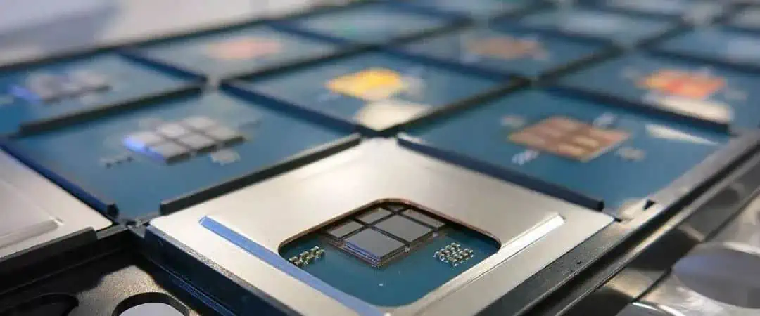
FPGAs are gaining popularity due to tier-unique features. You can find several FPGAs in the market with different specifications and features. Today we are talking about XC6SLX45-2FGG484C. The manufacturer of XC6SLX45-2FGG484C is Xilinx, a leading company in Field-Programmable Gate Arrays (FPGAs) and related technologies. Xilinx is a well-known FPGA manufacturer, and the XC6SLX45-2FGG484C is one of the many FPGA models they produce. Moreover, It belongs to the Spartan-6 family. Let’s dig deeper to learn more about

Specifications of XC6SLX45-2FGG484C

This FPGA has 43,661 logic cells. These are the basic building blocks of the FPGA.

  • This amazing FPGA also has 6,912 slices along with 180 DSP Slices.
  • Mb block and RAM supports data storage. That’s why data storage is no more issue.
  • Four Clock Management Tiles are part of FPGA
  • It operates 400 MHz frequency

Alphanumeric Breakdown Of FPGA

Xilinx Evaluation Board

 Following the breakdown, the alphanumeric code XC6SLX45-2FGG484C is for you. Because many people consider these alphabets and numeric just numbers and alphabets, actually, they have significant means.

Here’s what each part of that part number represents:

  • XC Represents the product family, which in this case is the โ€“ Spartan6 FPGA by Xilinx. This company is well known for making programmable logic devices.
  • 6 represents the generation of the Spartan family. In this case, it’s the sixth generation.
  • LX45 indicates the device’s size and speed grade. In this case, it has 4,608 logic cells and belongs to the -2 speed grade. As a result, you may experience amazing speed.
  • 2 Indicates that -2 speed grade. It is moderate speed.
  • FGG484 Indicates the package type, which is a Fine-Pitch Ball Grid Array (FBGA) with 484 pins. Most of the FPGAs come in ball grid arrays. It is compact and easy to integrate systems.
  • C shows the temperature range of the device, which ranges between 0ยฐC to 85ยฐC. As a result, it can work even at high temperatures.
  • So, altogether, XC6SLX45-2FGG484C identifies a specific model of the Virtex-6 FPGA from Xilinx. Its code represents 45,000 logic cells, a commercial speed grade, and a Fine-pitch Ball Grid Array package.

 Advantages Of Using XC6SLX45-2FGG484C

1. Unmatchable versatility

One of the biggest advantages of the XC6SLX45-2FGG484C is its versatility. As an FPGA, it can be programmed to perform a wide range of different tasks. Unlike an Application-Specific Integrated Circuit, which is designed to perform a single function and cannot be changed once it’s been manufactured, an FPGA can be reprogrammed as needed. This makes it a great choice for applications where the requirements may change over time or where different tasks need to be performed on the same hardware.

2. Exceptional performance

ย How can an FPGA provide the best and most exceptional performance? It’s all because of its exceptional feature. That’s why it is advantageous to use XC6SLX45-2FGG484C. It gives you performance. It functions at a maximum clock frequency of 550 MHz; it can handle complex tasks quickly and efficiently. It also has a relatively large number of logic cells, i.e., 44,200. This number of logic cells is good enough to perform logic functions. A similarly large amount of Block RAM of 2,592 Kb makes it suitable for demanding applications.ย 

 Video processing or high-speed networking is an example of its high speed. Above all, it has a superior architecture.

3. User-Friendly Features

 Many people think that FPGAs are hard to handle. But this FPGA is easy to use. User-friendly features make it an ideal choice for FPGA. In addition, it also adds to its performance and versatility. The XC6SLX45-2FGG484C also has various features that make it easy to work with. For example, it has a built-in Power-On Reset circuit that ensures the FPGA uses normal power. It is initialized properly when power is applied. Moreover, it also has a JTAG programming interface. As a result, they can do easy programming and debugging.

4. Well-Organized Power Management System

Every FPGA comes with this unique feature. You can’t expect any FPGA without this feature. The XC6SLX45-2FGG484C FPGA also consumes low power. This FPGA features a dynamic power management system. That’s why it can adjust power usage based on the workload. Its dedicated power management interface is just the icing on the cake. It allows users to monitor power consumption in real-time. If the device is not working, then this system adjusts power. As a result, there is no power loss. The low power consumption of this FPGA makes it ideal for battery-powered applications. That’s why many IoT devicesย have this FPGA.

Some Frequently Asked Questions

FULL PCB MANUFACTURING Quote

ยท How Can a Hobbyist Use This XC6SLX45-2FGG484C?

The XC6SLX45-2FGG484C is a relatively mature product. As a result, there is a wealth of information available on how to use it effectively. This includes documentation, tutorials, and support from Xilinx and the broader FPGA community. This is a huge advantage for engineers who are new to working with FPGAs or who need to get up to speed quickly on a new project. That’s why you are a seasoned engineer or hobbyist. You can use it XC6SLX45-2FGG484C.

ยท What Is the Packaging Type of XC6SLX45-2FGG484C?

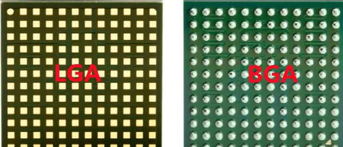
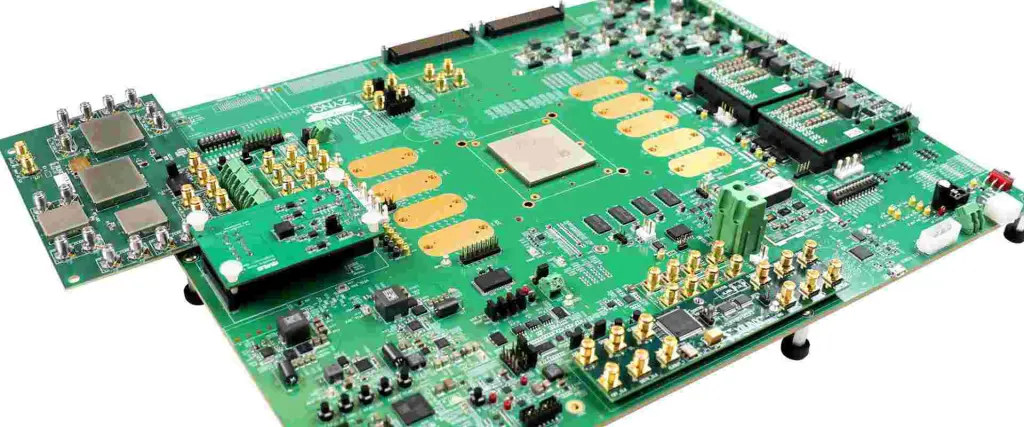
This FPGA comes in the FBGA-484 package. The ball grid’s airy and compact package makes it ideal for many devices. Most FPGAs come in FBGA packaging. It is based on innovative technology. BGA packaging is safe and compact. This packaging has a dimension of 23mm x 23mm. Above all, it is sturdy and standardized packing.

Concluding Remarks

XC6SLX45-2FGG484C FPGA has unique architecture. Its low power consumption and memory option make it ideal for various functions. As a result, it has better chances to incorporate in different systems.

Overall, the XC6SLX45-2FGG484C is a versatile, high-performance FPGA. As a result, it is easy to work with. Its combination of performance, flexibility, and ease of use make it a great choice for a wide range of applications. The scope of us is very high; for example, from video processing to high-speed networking to industrial control systems, it has the potential to adjust. Whether you’re a seasoned FPGA engineer or just starting out, the XC6SLX45-2FGG484C is definitely worth considering for your next project.

How Thick Should a PCB be?

Thick PCB

How thick should a Printed Circuit Board (PCB) and what is the baseline or standard for it? What are some of the reasons influencing the importance of a circuit boardโ€™s thickness?

A thick board can offer a wide range of benefits, such as supporting the resistance and conductivity capabilities of the PCB. Everything you need to know about the standard thickness, the benefits of the same and some of the special considerations are discussed in this article.

What is PCB Thickness?

It refers to the toughness or higher elasticity of the Printed Circuit Board (PCB). This has become a standard practice among many circuit designers, as it helps to increase the boardโ€™s resistance to damages.

What is Standard PCB Thickness?

It refers to the baseline or minimum thickness of PCB. Without this, it might be impossible to gauge whether the board can comfortably withstand some of the things and exposures it could have been exposed to.

The standard thickness is 1.577, which is the same as 0.062 inches. The reasons for the adoption include:

  • It is a historical standard size for circuit boards. It dates back to the days of Bakelite Sheets.
  • This standard thickness is also used across different facets, especially in the electronics industry, where it is used for both consumer electronics and related products.

The Variations to Standard PCB Thickness

pcb copper thickness

Despite the historical advantage and the widespread usage; the 1.57mm size is not the only one you can find out there. Today, different variants are in existence. Examples are:

  • 3.17mm or 125 mils
  • 2.36mm or 93 mils.
  • 0.031 inches or 0.78mm
  • 0.03 inches or 2.36mm

What is the PCB Thickness Tolerance?

The ideal tolerance is 10% for the base thickness of 1.57mm. The tolerance can also vary, depending on the applications, the types of circuit boards and a couple of other design and manufacture factors.

How to Determine the Thickness of PCB Layers

The layers of the circuit board also have a role to play towards the accurate measurement of the thickness. For context, the higher the number of layers used, the more difficult it becomes to get the right dimensions.

The layers of the PCB can range between 2 and 32. Out of this, the considerations for the thickness range from resistivity, conductivity and mechanical weight.

PCB Copper Thickness

The copper (material) used in the circuit board can also influence the thickness of the board. Mostly measured in ounces, the thickness of the copper ranges between 0.5 oz and 2 oz. it is also common to have the measurement ranging from 1 oz and 2 oz.

The Factors Influencing Thick PCB

FULL PCB MANUFACTURING Quote

A circuit board is not thickened without a purpose. Certain factors, parameters and considerations influence how thick the board becomes.

The following are some of the common factors, broken down based on the roles they play:

1. The Design Factors

How the PCB is designed can influence the outcome of the thickness. Here are examples of the design-centric factors:

2. Copperโ€™s Thickness

Also called the copper weight, it refers to the relationship between the current passing through the board and its thickness.

Measured in ounces per square feet, the base copper thickness is between 1 oz and 2 oz (1.4 to 2.8 mils).

However, the thickness of the copper can be modified depending on the following factors:

  • The addition of more copper, depending on the increased need to increase the currentโ€™s thickness.
  • The layer of the PCB increases as the weight/thickness of the copper increases.

3. Signal Types

What types of signals do the circuit board carry? Variations in the signal influence the boardโ€™s thickness in the following ways:

  • The type of required signals impact the types of materials the board uses.
  • Depending on the materials, the boardโ€™s weight can increase, especially if more (thick) materials are used.

The types of circuit boards are also considered here. For example, the High-Density Interconnect (HDI) boards using complex signals often have thinner footprints, thanks to the combination of the following:

  • Thin, high-performance materials.
  • Laser microvias and;
  • Thin traces.

On the other hand, the PCBs conveying high-power signals tend to be thicker, thanks to the following factors:

  • These boards use wider traces.
  • They also use thicker copper.

4. The Type of PCB Material

What type of material does the circuit board use? It plays an important role in the thickness. Worthy of mentioning is that the Flame Retardant 4 (FR-4) material is commonly used because of the flexibility and availability of the substrate in different thickness options. You can find the FR-4 materials ranging between 0.2mm and 3.2mm.

5. Size and Flexibility Concerns

The type of material used also has a hand in the outcome of the boardโ€™s weight. Worthy of mentioning is that the considerations are between the thinner and thicker boards, all based on the materials used.

The following are some of the discrepancies between the thick and thin circuit boards:

  • Rugged vs. Thin: thin circuit boards, such as the ones using the flexible materials are flexible, but pose a risk of lacking structural integrity. On the other hand, the thick PCBs are rugged.
  • Space Considerations: thin PCBs tend to take less real estate in the circuit board, because of the flexibility. The reversal is the case with the thick PCBs that take up a lot of spaces within the boardโ€™s real estate.

6. Viasโ€™ Type

The footprint created by the vias also plays a part in how thick the PCB becomes. Via in-pad, through via, buried via, blind via, and micro via are the common types of vias.

Despite the fact that these vias help to fast-track the routing of traces through the boards; they can also impact the size. For example, it is better to use the micro vias for the HDI circuit boards and the PCBs with thinner footprint.

7. How Many Layers Does the PCB Have?

The numbers of layers used in the circuit board also impact how thick it becomes. The general rule is that multiple layers equal more weight. Therefore, a multilayered PCB tends to weigh more and be thicker than one that uses a single layer.

  • A single-layer PCB weighs around 1.6mm, while the standard PCB thickness for 2 layers is higher.
  • Ideally, the 2-layer, 4-layer and 6-layer circuit boards often fall within the ambient of the standard PCB thickness.

8. The Operating Environment

Circuit boards adapt differently, based on the environments they are exposed to. Some contexts are given below:

  • Due to the less thermal stability, the thickest PCB is best used in low-current operating environments.
  • Both the flexible circuit boards and the ones with a thinner footprint are not ideal for use in rugged operating environments.

The Manufacturing Factors Influencing PCB Thickness

copper thickness

The processes that go into the production of circuit boards also impact how weightier the circuit becomes.

These are some of the manufacture/production-centric factors influencing the boardโ€™s weight:

Depanelization Method for the PCB

Depanelization refers to the process of separating jointed PCBs into individual circuit boards. Depending on the type of board, different depanelization methods should be used.

  • It is better to route the thinner PCBs, as a way of creating breakaway tabs.
  • The scoring depanelization method can be used to separate the thick circuit boards.

The Drill Hole Manufacturing Process

This has to do with the relationship between the drilling process and the underlying factors for making such holes in the PCB.

These are some of the considerations:

  • Aspect Ratio: this is the ratio or figure highlighting the difference between the drill hole diameter and the holeโ€™s depth.
  • The depth and diameter capabilities of the lasers and drilling machines also influence the hole-drilling manufacturing process.

Layer Stackup

How the layers stackup or are outline on the PCB? The PCB manufacturer should be able to create stackups of the layers, especially for the PCBs with thinner footprints.

End-Use Environment

Where will the thick PCB be exposed to or used at the end of the day? The rule of thumb is that the harsher the environment is, the higher the thickness of the circuit board should be.

A harsh PCB environment is underscored by the following:

If your PCBโ€™s use case is required for any of those environments, it means that you need to fortify it with more layers. This makes the board thicker, weigh more and have enough coverings to bolster the durability and reliability.

The PCB Assembly Process

The completion of the circuit board production process is not deemed over if the components have not been assembled.

At this point, the processes that go into the Printed Circuit Board Assembly (PCBA) have a role to play in the thickness.

Here are some noteworthy considerations:

  • The Wave Soldering process is best-suited for PCBs with thicker layers.
  • Consider using the Reflow Soldering process for the thinner circuit board layers. Doing so helps to aid heat or thermal energy transfer in the PCB.

Conclusion

The thickness of copper layer in a PCB can increase the boardโ€™s weight. Therefore, you should explain your layer requirements to the PCB Contract Manufacturer (CM). We will take your requirements into considerations, as a way of ensuring that the capabilities of the materials match the final PCB design.

What Does a Pick and Place File Mean?

Pick and Place File

This component placement list and Pick and Place File is very important for the right utilization of the pick and place machines. The pick and place data are necessary for the proper placement of the through-hole and surface mount parts on the circuit boards. This pick and place data can be described as the machine file that takes the text format of ASCII. This is composed of the X/Y locations, reference designator, rotation, the bottom or top side of the circuit board, etc.

The XY position or pick and place files are very useful for the automated placement of the SMT component. Also, you can program the pick and place machines manually, making use of a special camera guide. However, this could take a very long period, especially for boards having lots of components, which could lead to errors. With the Pick and Place file, you will be able to improve your accuracy as well as save time.

Pick and Place files can be basically described as the components present in their design as well as their x-y rotation and coordinates. Majority of the PCB design softwares can also help in extracting the orientation and location of the component from the layout file of the board. This produces your pick and place file.

KiCad Pick and Place File

.Schematic File

Whenever you want a machine to assemble YourPCB, you can create the position file for that machine to know where each part will be placed. The KiCad process could be a bit tricky; this is why we have decided to create a comprehensive article to assist you with the generation of a position file.

The first step is placing the โ€œPlace File Originโ€™. Search for โ€œPlaceโ€ and then select drill/place file Origin. Next, place this origin in the boardโ€™s lower left-hand corner side of the board. Note that, if it doesnโ€™t take a perfect spot in that corner, then it is nice so far it remains close.

Check the PCBNew section, select โ€˜Fileโ€™ and then select โ€˜Fabrication Outputs.โ€™ Then from there, choose Component Placement (denoted as .pos).

During the generation of these files, male sure that these settings are in place:

  • Format โ€“ASCIIUnits โ€“ Millimeters
  • Files โ€“ Separate the files for the back, front
  • Check โ€“ Make use of the place/drill file origin

There would be two different .pos files created. One of the files would be for the top part of the board while the other will be for the bottom part of the board. Now, these are the important files that we cannot but make use of.

What is the Pick and Place File Composed of?

Now, let us consider what the file is composed of.

  • Ref: This is the designator for your component. It is usually set in a schematic builder
  • Package: It is the footprint used when you are laying out your PCB
  • Val: This is the value of the component. It is usually set in a schematic builder
  • PosY: It is the Y-position with respect to its place origin
  • PosX: This is the X-position with respect to its place origin
  • Side: This is the side of that port where the part is on. Note that you must have two different files for the bottom and top.
  • Rot: It is the number of degrees that the part has to be rotated using the machine during assembly

If thereโ€™s a need to make changes to the .pos file, make sure you donโ€™t alter the file created. Only make changes in the layout and then create a new.pos file. The generated file is fed into the pick and place machine and it might not function effectively if you make changes to the format.

How to Generate Altium Pick and Place File

FULL PCB MANUFACTURING Quote

Accessing the Setup

You can access the dialog of your Pick and Place Setup in these ways outlined below. Click on File, then select Assembly Outputs, and then choose โ€œgenerate pick and place files from the PCB.โ€ Under โ€œAssembly Outputsโ€, which is seen in the Outputs section of the OutJob (denoted as *.OutJob), click the โ€œgenerate pick and place filesโ€ twice.

All Columns: This explains all the parameters where you can select from to be added to the output file. Then enable the parameterโ€™s Show column which you wish to add to the output. Also, the information of the location can be expressed in three different ways. This corresponds to those three methods though which the reference point of a component footprint may be specified inside your source PCB library.

  • Mid X, Mid Y โ€“ This coordinates for the center point of the component
  • Ref X, Ref Y โ€“ This coordinates for the user defined reference point of the component
  • Pad X, Pad Y โ€“ This coordinates for the Pad 1 of that component
  • The Grid Region: The grid region shows a preview of what information would be added to the output file.

Output Settings

Units: This region is used for specifying if you should use metric or imperial units when measuring the location coordinates of the component

  • Show Units: This shows the units
  • Formats: This shows the different formats (Text and/or CSV) from which you wish to generate the output.
  • The Separator: Choose your preferred unit separator out of the drop-down
  • Exclude the Filter Parameters: This enables the exclusion of the parameters utilized for the filtering
  • Include the Variation Component: This feature enables you to add variants.

When you click Ok, you will generate the pick and place files (.txt and .csv). These files would be stored in line with the defined output paths.

These files would be seen in the Projects Panel, which is located under the projectโ€™s Text/Generated Documents sub folder.

Tips

The dialog offers the capability to integrate custom filtering in order to remove some certain parts from the report. You need to select the filter icon to apply filtering. The filter icon is in a column header. You will realize that the subsequent menu comprises row entries to enable quick elective filtering. All you just need to do is to select the custom entry. This helps you to have access to the Custom Filter dialog.

Furthermore, you can integrate the dialog to indicate the rows of data to be displayed in the BOM according to the filtering criteria. The filter icon will change its color to blue once you have applied it. This means that the column in question is experiencing custom filtering. As required, add custom filtering to the other data columns.

What is the Significance of the Pick and Place File?

Pick and Place Files play a very significant role in the process of PCB assembly. Typically, it features the line number of the BOM, XYZ coordinates, reference designator, as well as each board componentโ€™s part number.

Also, the pick and place file is very important for the selective soldering and SMT placement machines. This happens before the process of assembly starts.

The circuit boards come manufactured in panels. Also, it is very important that you update your pick and place files continuously after each change has been made on your board.

Instructions Necessary for Pick and Place File Creation with Different Software Types

named pick place with .csv format.

Eagle Software

To create your pick and place file, run mountsmd.ulp. You may be able to view this file from the menu. Choose File then run the ULP from your dropdown list. This software would create this .mnt (mount top) as well as .mnb (mount reverse). The file also maintains the componentsโ€™ location coupled with the PCB originโ€™s coordinates. This file will be in txt format.

The Altium Software

The altium software is useful for creating an output for the pick and place that will be utilized during the process of assembly. To create the output, two options are available.

Create (*.outjob), which is the Output Job Configuration file. This creates an output generator that is well configured. Choose File from your menu. From your dropdown list, select Assembly Output, then โ€œGenerate Pick & Place Files.โ€

Once you click Ok, youโ€™ll see your output in the dialog box of your Pick and Place Setup. Note that the settings will be stored and kept safe in the config file. Moreover, when making use of the dialog of the Pick and Place Setup, these settings will be stored inside the project file.

Allegro/OrCAD Software

There is a similar procedure for the creation of pick and place files for either Allegra or OrCAD software. Select File from your menu. Then from the dropdown, click โ€œExportโ€ and then โ€œPlacement.โ€ Note that this procedure works with the most recent versions of Allegro or OrCAD software. The earlier versions might be different. Make sure you consult the documentation of the user to get more information.

Conclusion

In order to place the surface mounted components on the printed circuit boards through automated equipment, creating the pick and place file is very necessary. This helps in programming the equipment. The pick and place file has all the necessary positional parameters that this machine will know where this component will be placed as well as the orientation it would be on the printed circuit board.

A Guide to Comparison between PCB Potting Vs. Conformal Potting

pcb potting

Today, there is no electronic device existing that does not contain PCBs in its structure. The quality of the PCBs used in such devices directly relates to the normal functioning of the electronic devices later.

 It means all PCB manufacturers need to pay great attention while designing and producing PCBs. It is because the performance of minor to major electronic devices enhances with these PCBs. 

One way to make sure that the manufacturer is producing state-of-the-art PCBs is called PCB potting. In this post, we are going to have a detailed look at critical aspects of potting and how why it is important to ensure the quality of PCBs for integration into electronic gadgets.ย 

What is PCB potting?

pcb potting compound

You can define Potting for printed circuit boards as a quality-check method that minimizes any chances that can damage electronic devices due to faulty PCBs. There are different external factors like chemicals, heat, and mechanical wear that can lead to further damage if not treated in time.

 The process of potting includes a special potting material that functions similarly to a chemically formed encapsulation resin that secures the entire PCB board from the aforementioned complications. 

Now, letโ€™s discuss some prominent advantages of PCB potting below:

  1. Improves performance: One major benefit of using PCB potting is that it maintains the natural performance of electronic devices. It also boosts the circuit’s dependability by securing the printed circuit boards from possible threats, which include voltage issues, moisture, and alteration. Sometimes other factors like vibration and stress can create a negative impact on electronic devices, and potting helps with that as well. 
  2. Reduce vibrations: It means potting blocks the vibrations created due to printed circuit boards and their holders. In case these vibrations exceed the limit, they can exert stress on the printed circuit boards and lead them to ultimate dysfunction. 
  3. Tidy PCBs: The printed circuit boards can inculcate debris and dirt due to prolonged usage. Potting includes an encapsulated resin that helps in keeping the board tidy through all circumstances. Dirty and uncleaned PCBs can absorb more heat and hinder the signals, which hamper the performance of the electronic gadgets you want to use in. 
  4. Privacy: Electronic devices cannot function properly if they lack security. For this, PCB potting is the best possible solution. The process makes the PCBs accessible and combines with engineering to ensure impeccable protection of PCBs. 

Compound Guide for PCB Potting

Common Compounds

1. Epoxy

Epoxy is among the favorite potting materials used by many PCB manufacturers. It is because it offers different benefits. It is better to have a quick look at the following benefits offered by Epoxy resins for the potting process:

  • Epoxy has no parallel when it comes to adhesion
  • Such resins do not need primers that speed up potting for PCBs
  • They are excellent in tensile strength and stiffness
  • Epoxy resins are good for use in transformers and agricultural machines due to their impressive chemical properties. 

2. Silicone

Silicone is another trusted potting material common to use. There are different applications of silicone except potting for PCBs. You will see different PCB manufacturers relying on silicone for potting. The following pointers will help you understand why is that:

  • Silicone is good for potting because it has an impressive expansion ability
  • Silicone is soft, and you can easily amend it in any desired form
  • The temperature endurance of silicone stands the best when it comes to potting
  • Silicone is not an affordable potting compound, but it does not exert any stress on the PCB components at all

3. Polyurethane

We have Polyurethane which is among the commonly used potting materials. There are different reasons why Polyurethane is on this list. Letโ€™s find them out below:

  • Polyurethane is an expandable material that fits best for potting
  • It resists mechanical wear and possible damage to PCBs and their parts
  • It goes well with different natures of substrates due to its excellent flexibility

Merits and Demerits of PCB Potting Assemblyย 

FULL PCB MANUFACTURING Quote

The method of potting is not a hectic one to perform. It is among a few effective and fruitful PCB-relevant processes that drive out positive results. Especially those PCBs that need a durable quality check method; there is no better option than potting itself. 

The technique is also suitable for devices that need to avoid mechanical abrasion all the time. Potting enhances the longevity of these devices at the same time.

 Experts believe that you can also consider a potting method to make sure vibration dampening, regulated heat emission, and protection of PCBs and their components are in place.  

Choosing the Right PCB Potting Material

ยท Hardness

Since there are different potting materials available in the market, donโ€™t get stuck with choosing the best for yourself. One main factor in evaluating potting compounds is their hardness. 

  • If a potting material is tough, it will provide better protection against weather complications like heat and moisture
  • Hard potting materials are epoxy and urethane, along with silicone
  • Siliconeโ€™s hardness ranges from 10A-60A, and it’s the hardest material you will find on the market

ยท Thermal conductivity

Another factor is the thermal conductivity. You need to make sure that the potting compound you are going to select meets the following standards of thermal conductivity:

  • The compounds with an acceptable range of thermal conductivity are useful for potting.
  • Epoxy and urethane can prove to be beneficial in terms of delivering a good amount of thermal conductivity.
  • Silicone is the best with thermal conductivity and dissipates a large amount of heat produced by electronic devices, whether big or small. 

ยท Viscosity

A fine potting material must have the parameters of viscosity. In case you don’t know about them, check out the following pointers to learn about viscosity standards in detail:

  • The perfect encapsulation of PCBs works flawlessly if the viscosity is less.
  • If the potting material is self-leveling, it will contribute to achieving positive results.
  • The potting compound should be easily adjustable to avoid any problems, and this only happens if the viscosity of the compound is less.

ยท Color

You cannot ignore the color of the potting material. Such compounds come in different colors, and each varies as per your situation. Letโ€™s see how you can weigh down potting materials on the basis of their colors:

  • Choosing an appropriate color of the material is necessary to enhance the presence and quality of the PCBs
  • Sometimes obscure compounds can prove to be helpful in this aspect
  • If you want to emphasize the LED visualization, then always go with the transparent potting materials available 

Step-by-step guide for PCB Potting

  • Pre-baking

One of the resins used for this process is POLYOL. However, polyol does not settle down with moisture easily at all. Due to this reason, if you’re using polyol, make sure to pre-bake the container. 

Now, this pre-baking step will remove the slightest moisture present in the container. If you ignore pre-baking the container, the polyol will not be able to function naturally due to the presence of moisture inside the container. 

  • Marking the resin level

The amount of resin used for potting is crucial to determine. For this, if you mark the resin level, it will save you from possible fuss. So always mention the resin level on the container you are using. Plus, you also need to protect critical components of the PCBs by securing them from confronting abrasive damage when potting takes place. 

  • Preparing the resin

It is important to combine POLYOL and ISOCYANATE to develop a fine resin for potting. To do this, it is better to cover your face with a mask and wear neoprene gloves to save your hands and skin from this chemical reaction. 

Now it’s time to extract a flexible compound from these two materials by keeping the ratio 1:6 for isocyanate and polyol. Now keep stirring the polyol with a metal bar to not let it accumulate due to fluctuations in the external environment. 

Make sure you weigh the container in the first place before you add polyol to it. Now add polyol and mark down the change in the weight and keep adding the polyol once it reaches 6/7 of the weight of the resin you want to use for potting process.

 Repeat the process with isocyanate but limit it to 1/7 of the weight of the resin you need to prepare. It’s time to merge both compounds by stirring this newly formed mixture. 

  • Pouring the resin

The next step is to add this resin mixture to the PCB container. Keep the bucket tilted at a 3-degrees angle. If you keep a smooth pad under the container, you can make the exact angle to avoid any troubles. 

Now start pouring this resin into the PCB container till it reaches your marked level. Leave the entire setup at room temperature for a while and wait. After some while, put this setup into an oven and bake at 80 degrees for at least one day.

  • Checking the final quality

Next day, you need to take out the PCB container from the oven. A special tool called Analog Shore which helps in analyzing the hardness of the resins, will assist you in testing your resin finally. 

The shore should show the reading to be within 85-90. If you get this reading, it means the resin you have prepared is suitable for the potting process.ย 

Different Between PCB vs. Conformal Coating

PCB-circuit-board-waterproof-coating

In this section, we are going to compare regular PCB potting and conformal coating. However, it is important to know the major differences between the two so that you can find out what type of methods will be suitable for you as per the situation. 

There are different use cases for both these methods. Due to this reason, we are going to make it easier for you to choose the best method for easy implementation. 

Before we hop onto their differences, letโ€™s see what similarities between these two methods are:

  • Both techniques are beneficial in protecting the substrate from external factors like a moist environment, excessive vibrations, and rapid corrosion.
  • Both methods promise better results and can prove to be fruitful with the final product.

Below are some major differences between the two methods:

  • PCB potting is better for those devices that function on the basis of fewer vibrations, minimal abrasion due to interaction with chemicals, and heat dissipation. Potting works best for those devices that are robust and often face challenges like the above. 
  • The resins used for potting process are excellent for avoiding electrical glitches. Due to this reason, one of the major use cases of PCB potting is integration in high-voltage electronics. 
  • Conformal coating, as compared to potting, is a slow and hectic process, whereas potting takes place smoothly in a short period of time. 
  • Conformal coating never requires repairing and checking, unlike potting, which can create a negative impact on the components of PCBs.
  • The conformal coating also does not exert any pressure or stress on critical or minute PCB parts like pins, wires, and screws, unlike potting, which can compromise your substrate.
  • You can easily perform conformal coating in a small enclosure which works on minimal devices, which is not true for PCB potting that only, takes place in large containers. 

Which Potting should you choose for Better Results?

 Now you might be wondering what type of method you should go for that promises better protection for PCBs.

Letโ€™s find that out in this section:

For PCB potting:

  • The protection of PCBs mainly depends on the type of potting resin you want to use and also the type of product.
  • It is important to understand and learn about the potting resin completely to make sure it performs well and does not compromise the process at any cost. 
  • During the process of potting, it is crucial to regulate the temperature and maintain it within a suitable range to avoid complications. 
  • One drawback of this process is that when you merge the resin with the hardening substance, it will give out a large amount of heat that entirely disrupts the PCB structure.

For conformal coatings:

  • If you consider conformal coatings, you must know the resins differ in their resisting power. 
  • In most cases, water does not harm the resins, but double-checking the resin proves to be helpful.
  • Resins used in conformal coatings absorb the trauma and protect the PCBs from possible damage.
  • However, there are some definite downsides of conformal coatings as well, such as more velocity can damage the PCBs and might also leave impressions on their structure in extreme cases. 
  • The conformal coating method is good for designing in a freehand style.
  • Such a method offers complete securing of electronic devices irrespective of daily usage.

Factors to Consider While Designing PCB Pottingย 

Conformal Coating
Conformal Coating

The designing criteria for conformal coatings and potting require your attention as we move toward the conclusion of this discussion. 

  • If you develop a film of resin on the upper surface of a PCB, it will increase its weight.
  • If the resin is more rigid, it will not let the electronics perform in a natural way.
  • Such a resin which is rigid and inappropriate, will exclude any margin of future changes if needed. 
  • Now if you try to exclude a pre-attached rigid resin from the PCB, it will damage it and can cause irreversible abrasion as well. 
  • Some coatings are transparent, which makes their usage easier and faster during the technical PCB assemblies. 
  • Such coatings can prove to be useful in protecting sensitive parts of PCBs. 
  • You can use a brush or spraying bottle to add the coating to PCBs or simply submerge the PCB into the coating.
  • You can replace encapsulation with these coatings to ensure complete protection of PCBs without spending extra on cost. 

Closing Words

You must know by far that both these methods are crucial to increase the life length of advanced PCBs. These methods are cost-efficient at the same time. 

However, some factors, like their pros and cons and the complexity of both these methods, might give rise to newer and much easier technology for protecting PCBs. Hopefully, now you can easily choose the best technique and get your projects running in no time! 

How to Use the Fritzing PCB Design Software

Fritzing PCB

Fritzing PCB design software can be described as a reliable open-source tool which anyone can share, teach, as well as prototype their personal electronic projects. Also, it permits users to design the schematic, which could be included in the professional looking wiring diagrams. Users can even design their own printed circuit boards and also fabricate them from your designed files. Fritzing software can be used in hook-up guides, classrooms, as well as other places that need to teach ways of hooking up boards to other types of hardware.

Another significant aspect involving the creation of new projects involves the initial designing as well as vetting process so as to know if the circuit would function or not. Furthermore, this tool offers users with schematics, design, and creation of the PCB layout. Letโ€™s continue with the topic and understand what Fritzing PCB can offer users.

What is Fritzing PCB Design Software?

As mentioned earlier, Fritzing PCB design software offers a free program used for designing circuits on the breadboards, create the schematics, as well as develop the printed circuit boards. In contrast to many circuit design suites, it heavily utilizes vectorized images, creating great looking circuits.

Fritzing features so many well-known components like the Arduino modules and boards. It is specially designed for hobbyists rather than for professional use. Coupled with its free design qualities and features, it also has a projectsโ€™ page and community forum whereby users can easily upload their individual projects.

How to Design a Project on the Breadboard

Hardware Layout
Hardware Layout

The breadboard view is the first major window seen in its environment. This allows the easy creation of the breadboard circuits. Also, you can adjust the size of the breadboard. It has an interactive set up; this allows users to drop wires and components to the individual pins.

Furthermore, the window seen on the screenโ€™s right hand side allows users to locate as well as place different components on the breadboard. The search also allows specific parts to be located easier. In contrast to circuit suites that are more advanced like KiCad, the available parts are limited to commonly used microcontrollers and modules.

The parts seen in the search window will be dragged in the area of the breadboard and will snap in the holes as legs cross them. Whenever parts are dropped in place, the electrically connected rows to the component legs appear.

This allows easy identification of the rows and clearer placement of the wires. Users can choose wires as well as change the color. The changing of the wiresโ€™ color is a great practice with heavily-reliant designs on wires. Also, its inspection window, located below the search window of the component, is useful for editing components, which includes the breadboard.

The Creation of the PCB Layouts

This is the final stage when creating circuits using Fritzing. Similar to its schematic stage, these PCB parts are placed automatically on the circuit board. Also, the user needs to position and orient these components.

This stage of PCB isnโ€™t compulsory because not all projects will make use of a PCB. Using Fritzing PCB design software comes with a major disadvantage which is the software working hand in hand with the Fritzing PCB service that turns the Fritzing design into low cost PCBs easily.

Like the schematic layout, you can rotate and drag the components with their neighboring indents. This PCB can be resized easily by dragging its corners. This inspector window offers more options like the number of layers present on the printed circuit board as well as the shape (like the shield shape of the Arduino).

You can route copper tracks by double clicking on the dotted lines, as well as by clicking and also dragging from its pads. When manual routing becomes too difficult, you can use the auto-router in Fritzing which automatically routes the PCBs.

Whatโ€™s In the User Interface of Fritzing?

Immediately after opening Fritzing, you will see a pleasant and easy interface.

Welcome/Home Screen

Here, this is what you see when the program is opened. This basically reveals recent projects. At the right hand, you will see the blog area as well as related news, including latest versions, platform news and some important publications regarding Fritzing.

At the right side of the home screen, youโ€™ll see the components section. This is where you can see the whole electronic catalog used in their projects. These are categorized depending on their nomenclature and use. Also, you can make use of the search bar; this gives the filtering facility depending on whatever needs to be used.

Breadboard

Immediately after selecting the components, there is a need to place the components on the breadboard or test board to create the electrical connections. Breadboards are boards having holes, which are connected electrically. The power lines also follow a specific horizontal pattern.

Also, the lines for component connection follow a special vertical pattern. With this, connections can be created in a safe and logical way, making sure that the project functions well before the PCB is manufactured.

PCB

Here, you will see the way the basic circuitโ€™s PCB model will look like. Clearly, this is the PCB design which is sent to be directly printed from that program with the respective cost. There are some rules to take into account when placing and wiring the components on the printed circuit board. These rules correspond to the temperature dissipation, wires, size, etc.

Schematic

To comprehend this section, there is a need to understand the schematic diagram concept in electronics. Usually, this schematic diagram relates to the circuit. The diagrams are also referred to as circuit diagrams or wiring diagrams and reveals the way in which the circuitโ€™s components are connected. The lines indicates the connecting wires, while the remaining elements like switches, lights, and resistors are represented by some standardized symbols referred to as the electrical schematic symbols.

Code

This final section is primarily dedicated to the users using Arduino boards for their electronic projects. Here, Fritzing allows you to create that code you wish to integrate in the physical microcontroller. Physical is emphasized here because the program doesnโ€™t allow any simulation in its features.

What are the Pros and Cons of Fritzing PCB Design Software?

Fritzing comes with lots of benefits. However, it comes with some disadvantages as well. To make the right decision it is advisable that you know both the good and bad about Fritzing.

Pros

This software program lets designers as well as other professional record their created prototypes for different circuits as well as the design corresponding circuit boards.

You can also make use of the website of the company to communicate personal drafts and ideas with others. Others may decide to create their electronic items using your prototypes. This sharing concept helps in the reduction of production costs.

One important benefit of the Fritzing PCB software is that amateurs can design their circuits and create PCBs that suit their needs. They can find all the needed great in the Fritzing PCB design software store.

Other benefits include:

  • It is free
  • Great for Arduino board-based projects
  • Lots of electronic devices and features to be used in the library
  • Large development of users and the community
  • It is open source

Cons

  • The Fritzing PCB is Arduino-specific in several ways
  • There are other shortcomings in the other EDAs like the impossibility of having to stimulate as well as test your prototypes.

Whatโ€™s up with the Latest Version โ€“Fritzing 0.9.3b?

FULL PCB MANUFACTURING Quote

The Component Library is Updated

The Fritzing library is stored online now on GitHub and checks for updates automatically. Therefore any software upgrade is available to the users automatically. This creates the pathway for the direct contributions of the user.

Bugs are absent

Initially, bugs appearing in the PCB traces usually mess up with the other tracks exiting in the layout. This makes it very difficult for the designers to discover any error in the circuit. This software also permits high-DPI display. This allows you to see it easily.

Self-handling of the customized tools

Initially, the customized parts were stored inside a hidden location. This made editing using external tools to be difficult for designers. However, these parts are located conveniently inside the Fritzing folder located under Documents. This makes the work very easy for the users. Just like the Pad2Pad, the user will be able to order their printed circuit board to be manufactured on the Fritzing Fab. This saves money and time on the developer boards that would have been gotten from the other manufacturer.

Conclusion

The Fritzing PCB design software is simply a free automation electronic design program, which is specifically designed to assist artists as well as designers in transiting from the prototypes (for example, using the test board and to the final products). The creation of Fritzing PCB design software works with the principle of Arduino, which allows the researchers, artists, designers, as well as hobbyists to be able to register their personal Arduino-based prototypes, as well as create diagrams for their printed circuits for fabrication.

A Comprehensive Overview of WLCSP: Wafer Level Chip Scale Packaging

WLCSP

Wafer Level Packaging, also known as WLP, is a subcategory of IC packaging technique that is suitable for wafer level. You cannot cut the wafer without packaging. Instead, it is important to first cover the wafers with packaging and then cut them through. 

Before cutting the wafer, it is important to add special bumps while assembling the components. WLP is a simple and cost-efficient process. There are different steps in the WLP that need precision. 

These are wafer fabrication, wafer testing, and analysis. WLP is also reliable when you need to make sure everything is in place, from procuring the raw materials to shipping the final product to the customers. 

The process is also known as Chip scale packaging and can be divided into two further sub-categories called fan-in and fan-out packaging. 

In the past times, people used wires to combine the semiconductor chips and their substrate together.

 It is important to do this on the periphery of the semiconductor as problems majorly arise from the edges. Now this whole process is wire bonding of semiconductors. Sometimes things can go south, and you might end up facing two issues while doing wire bonding. 

  • The electrical conductance can be too low during the process
  • Less number of wires used for each chip 

Now poor electrical conductance eventually disrupts the performance of high-frequency devices, and insufficient wires hamper the data transmission of the chips as well. 

People started to find portable semiconductors and circuits not appropriate as their wires were thin and too long, which increased the power losses and lagging. 

Now this led to the invention of flip chip packaging, which was a one-stop solution to major problems that occur during wire bonding. The flip-chip method made the manufacturers use bumps instead of wires for the purpose of connections.

 You place these on top of the wafer, which increases the electrical density throughout your setup. After this, you cut the wafer and flip the chips to combine them with the substrate by using special copper pillars.

ย WLP is the simplest technique that most producers rely on today. Major giants in the semiconductor industry use WLP to ensure positive results.ย ย 

Types of WLCSP: Wafer Level Chip Scale Packaging

LGA-vs-BGA

 WLP has two major divisions. These are fan-in and fan-out types. The interposer is the main factor that differentiates these two types on the whole. For the fan-in type, you keep the sizes of the die and interposer the same.

 For the fan-out type, the interpose is always bigger than the die. These processes are also different from a standard WLP package because you apply the interposer on these types directly, which does not happen in the WLP. You can even cover the die and interposer for these two types to protect them under stressful and non-favorable conditions.  

Benefits of WLCSP: Wafer Level Chip Scale Packaging

There are certain benefits of using the fan-out method in different applications.

  • It is reliable for producing TSVs that are silicon-made wires. These are highly cost-efficient and save enough energy when there is a need to achieve more electrical density. 
  • TSVs shrink the packages and make them slimmer without their quality at all.

Purpose of WLCSP: Wafer Level Chip Scale Packaging

  •  The main purpose of using the fan-out method is to draw out the same features of chips, even on artificial wafers. Such wafers use polymers that are affordable for production processes. 
  • Another purpose is to expand the space between the individual chips and their connections. 

Sub-categories of WLCSP: Wafer Level Chip Scale Packaging

You can carry out fan-out WLP in two different ways; letโ€™s check them out below:

 Chip-First: 

  • In this way, you need to incorporate the chips into a fine metallic entity. 
  • Now the next step is to perform the RDL as per its standards and guidelines. 
  • Chip’s first method is reliable due to its cost-effectiveness. 
  • Not only is its affordability attractive for the producers, but it also offers excellent performance in I/O devices and operations. 

Drawbacks of Chip First:

Despite the fact that the chip-first method is viable, there are some problems that might occur. It can lead to faults like die shift, die protrusion, and wafer warpage.

Chip-Last (RDL-First): 

  • In this process, you need to develop the RDL in the first place. 
  • Now, once the RDL is formed, place it on the wafer. 
  • After this, it’s time to develop the chips for melding them during the packaging procedure. 
  • Molding is important before you place the chips on RDL.
  •  The purpose of molding is to prevent the wafer warpage as much as possible.
  •  It is exceptional in electrical conductance and has an impressive pitch scale for your ease.

Drawbacks of Chip last:

  •  If you talk about the reliability of this process, it does not meet some of the industry standards that make it doubtful for usage.  
  • It also offers much less TSV potential as compared to Chip-first. 

Uses of WLCSP: Wafer Level Chip Scale Packaging

FULL PCB MANUFACTURING Quote

 Uses of WLCSP:

  • One major use of WLP is in I/O devices, as this industry is growing at a rapid pace. The industry stands only on fine interconnect density, and for that, there is nothing more reliable than WLP itself. WLP and RDL come together to offer durability and a certain boost to interconnect density for I/O applications. 
  • RDL is beneficial for the WLP process because it allows different chips to have exceptional features which will be later used in several applications. The encapsulations offered by RDL are useful for developing smartphones and other forms of semiconductors. 

Advantages of WLCSP:

  • WLP allows you to place chips on chips in vertical and horizontal positions
  • Due to the flexibility offered by WLP, different variants of ICs are now common.
  • The ICs developed from WLP are useful for finetuning the fan-out technology and sustaining TSVs when you use them for high-density areas. 
  • WLP is also reliable for increasing the bandwidth of your system.
  • WLP consumes less power as well. 
  • It is important for developing image sensors, AI devices, and IoT smart home appliances. 

Letโ€™s Explore XC3S1400A-4FGG484I FPGA.

wholesale Xilinx FPGA

If you are not new to the world of electronics, you may have come across the term “XC3S1400A-4FGG484I” before. Apparently, it seems number, but it is actually. Let me simplify things for you. It is an FPGA. FPGAs are different from integrated circuits.   Moreover, they are highly versatile and customizable. XC3S1400A-4FGG484I is one such FPGA with unique features and applications that set it apart from other models. Let’s dig deeper to know more about this FPGA.

 What Is XC3S1400A-4FGG484I?

XC3S1400A-4FGG484I is an FPGA. It is from Xilinx. This company is a leading manufacturer of FPGAs and other digital electronics components. You can find a long list of its products. This XC3S1400A-4FGG484 belongs to the Spartan-3A family of FPGAs. The spartan-3A family is a well-known family of FPGAs. Because of their high-performance architecture, and flexible configuration options,  they are outstanding. Its model number, XC3S1400A-4FGG484I, contains information about its specifications and package type.

 Technical Specifications of XC3S1400A-4FGG484I

  • It belongs to the Spartan-3A FPGA family.
  • It has 1400K system gates. These are the basic blocks of FPGA fabric. As a result, it can implement a large digital system. Thatโ€™s why its demand is increasing day by day.
  • It has 512KB of block RAM. As a result, it has a great memory for storing data in the FPGA.
  • It has 8 digital clock managers, aka DCMs. As a result, it can generate and synchronize clock signals. In addition, it improves signal quality.
  • It has 144 Input and input and output pins, that’s why it has a user-friendly interface with external devices.
  • It operates at a maximum frequency of 400MHz. As a result of this, FPGA can perform 400 million operations per second.
  • It has a 4-input lookup table architecture. That’s why complex logic functions are no harder to perform. As a result, you can implement complex logic functions so easily.

Alphanumeric Breakdown Of FPGA

FULL PCB MANUFACTURING Quote

Break down of numbers alphabet and numerics of XC3S1400A-4FGG484I. if you are new in the world of FPGA, then you may consider these just numbers. Actually, every digit and alphabet has some specific meaning. We are going to break down this alphanumeric code for your convenience. As a result, you can have a better understanding of this code.

  • XC3S1400A: This is the model or type of FPGA. In this case, it refers to the Xilinx Spartan-3 series, and the specific model is the XC3S1400A.
  • 4 refers to the speed grade of the FPGA. In this case, it indicates that the device is rated for a maximum operating frequency of 4 MHz.
  • FGG484  refers to the package type or the physical shape and size of the FPGA. In this case, it indicates that the device is packaged in a Fine-Pitch Ball Grid Array (FBGA) with 484 pins.
  • I indicate the temperature range for which the device is intended to operate. In this case, it indicates that the device has optimal temperature range of -40ยฐC to +100ยฐC.

Features of XC3S1400A-4FGG484I

XC3S1400A-4FGG484I has several features that make it stand out in the world of FPGAs. Some of its key features are:

ยท High-Performance Architecture

XC3S1400A-4FGG484I has a high-performance architecture. Thatโ€™s why it is easy to process data quickly and efficiently. It has up to 1,536 logic cells, and that is just icing on the cake. As a result, it can perform up to 266 million logic operations per second. Thatโ€™s so amazing. As a result, designers and engineers like it and consider it ideal for applications. Such applications require fast processing speeds.   video and image processing applications are one of the examples.

ยท Flexible Configuration

XC3S1400A-4FGG484I is highly customizable. You can make all the necessary changes according to the requirements. Integrated circuits are hard to customize or configure. That’s why FPGA is popular. Thanks to its flexible configuration options, you can now easily configure this FPGA. It can be programmed using a hardware description language such as Verilog or VHDL. Xilinx is also supportive in this matter. That’s why you can use this Xilinx’s software tools. These tools include ISE or Vivado, for the configuring. As a result, it allows users to tailor the FPGA to their specific needs and applications.

ยท Extensive Connectivity

The XC3S1400A-4FGG484I is a highly versatile device.  It supports a wide range of high-speed interfaces, Forexample DDR and DDR2. Similarly, it also supports interface DDR3 to some extent. Additionally, it is equipped with a built-in memory controller.   As result it can accommodate multiple memory types. For example, it supports SDRAM and SRAM. Similarly it supports FLASH memory type.

Moreover, the XC3S1400A-4FGG484I provides high-speed connectivity. As a result, it can support numerous high-speed communication protocols. These protocols include such as Ethernet, and PCI Express. This feature makes it a highly suitable FPGA for use in applications.   Such applications require fast and reliable data transmission.

One of the most impressive features of the XC3S1400A-4FGG484I is its programmable logic architecture. As a result, It allows designers to tailor the device to their specific needs. That’s why The logic blocks of the device are highly flexible and easy to reconfigure. As a result, it can execute an array of different functions.

ยท Digital Signal Processing  Capabilities

Furthermore, the XC3S1400A-4FGG484I possesses advanced Digital Signal Processing, aka DSP capabilities, which enable it to process high-performance signals with ease. The dedicated DSP blocks of the device can perform intricate signal-processing tasks. For example, it includes different tasks but is not limited to FIR filters. Further, it revolves around the FFTs and convolution. Signal processing matters a lot when it comes to FPGA integration with other systems or devices.

Final Note

Overall, the XC3S1400A-4FGG484I is a powerful FPGA. Designers and engineers like it to use for  In a  wide range of digital design applications. Its popularity is increasing due to its excellent features. That’s why if you are looking for an ideal FPGa for your next electronic project, then go for it. Its maximum frequency of 400MHz is great for high-speed devices. Similarly, its LUT architecture can make complex logic function implementation so easy. Above all, XC3S1400A-4FGG484I  is an ideal FPGa in all aspects.

What Makes NHI350AM4 NIC Different from the Rest of All?

NHI350AM4 Network Interface Card

Suppose you are a designer and looking for high-performance and reliable network interface cards. Then you may get confused by seeing different options. Some are low-cost, and some options are pricey with zero features. Let me tell you about NHI350AM4. What exactly is it, and what makes it so special? In this article, we will explore NHI350AM4 in detail.

 What Is Network Interface Card?

A network interface card, aka NIC, is a relatively new term for new hobbyist designers or engineers. But many of you may be familiar with it. It is a hardware component. It connects a computer to a network. It is also available in the market with the name of network adapter or LAN adapter. The NIC is responsible for communicating with other devices on the network. For example, servers, routers, and other computers. So you cannot connect to other devices or networks without NIC.

What Is NHI350AM4 Network Interface Card?

NHI350AM4 is a quad-port network interface card. As a result, it provides high-speed connectivity for data centers and cloud computing. In addition, enterprise-level applications also get benefit from it. As a result, it delivers high bandwidth and low latency. Moreover, you can expect high efficiency from it. That’s why it is an ideal choice for businesses. All businesses or applications require a reliable and high-performance network interface card can go for it.

The Key Specifications of NHI350AM4

Here are some of the key specifications of NHI350AM4. These specifications will help you to understand this NIC in detail.

  • This NIC has Four RJ45 ports
  • Its Interface type is PCI Express 3.0 x8
  • Data rate: is 10/100/1000/2500Mbps
  • It supports different Operating systems. For example, it supports Windows, Linux, FreeBSD, and VMware.
  • NHI350AM4 is based on Intel’s Ethernet Controller I350. In addition, it is a highly integrated Gigabit Ethernet controller. You can use it for high performance and low power. 
  • It is ideal for small form factor applications.
  • It is available in RoHS Compliant. Package
  • Operating supply voltage for this NIC is 3.3 Voltage

 Why Use NHI350AM4 NIC?

FULL PCB MANUFACTURING Quote

NHI350AM4 comes with a range of features. That’s why it is an ideal choice for businesses that require high-speed connectivity. The following reasons will be enough to tell you why you should go for it.

ยท High Performance and Low Latency

NHI350AM4 provides high-speed connectivity of up to 10Gbps, that’s why it is an ideal choice for different applications that require high bandwidth and low latency. It comes with four RJ45 ports, enabling multiple devices to be connected to the same network interface card, making it a cost-effective solution.

ยท Less Operating Cost

NHI350AM4 is ideal due to its energy-efficiency, reducing power consumption, and lowering operating costs. It comes with Intel’s Energy Efficient Ethernet aka EEE technology. It automatically reduces power consumption during periods of low network activity.

ยท Unswerving Quality

NHI350AM4 is a reliable and stable network interface card. As a result, it provides continuous network connectivity. In addition, it comes with a range of advanced features, such as link aggregation and load balancing. Similarly, it supports VLAN tagging. As a result, it ensures network reliability and unwavering connection.

ยท Hassel Free Installation

NHI350AM4 is easy to install and use. You don’t need to go through a complex process. Similarly, it has plug-and-play functionality. That’s why it comes with a range of drivers for different operating systems. What type of operating system you are using then, you just need to install drivers. As a result, it is easy to set up and configure.

The Alphanumeric Breakdown of NHI350AM4

 Alphanumeric breakdown talks about the alphabet and numbers’ signification and what they represent.

  • NHI is three alphabetic. That represents a manufacturer code, product line, or model name.
  • 350 is a numeric value that could indicate a specific product or feature within the manufacturer’s product line.
  • AM could represent a product variant, color, or other distinguishing characteristic.
  • 4 could indicate a version or revision number of the product.


Applications Of NHI350AM4 Network Interface Card

 It has a wide array of uses, but some important ones are mentioned below.

  • The NHI350AM4 Network Interface Card enables the connection of computers to wired networks. For example, Local Area Networks, aka LANs, and Wide Area Networks, aka WANs, through Ethernet cables. This NIC is ideal for swiftly transferring data between computers and servers. That’s why it supports high-speed data transfer rates of up to one Gbps.
  • Furthermore, the NHI350AM4 NIC is able to support virtualization technologies like VMware and Hyper-V. As a result, it enables multiple virtual machines to share the same physical NIC. Its outstanding Performance and reliability make it a common fixture in server applications. It can fix many problems with web servers and database servers.
  • Moreover, network monitoring and analysis are easy to carry out using this NIC. It allows allowing network administrators to troubleshoot network issues. As a result, it enhances network performance.

Technical Frequently Asked Questions

ยท What Is the Data Rate of NHI350AM4?

Data rates depend upon various factors. It varies from application and how you are going to use it.

The data rate of NHI350AM4 is 10, 1001000, and 2500Mbps, but it varies according to the situation.

ยท What Is Intel’s Energy Efficient Ethernet Aka EEE Technology?

Intel’s Energy Efficient Ethernet aka EEE technology is a feature that automatically reduces power consumption during periods of low network activity.

ยท What Operating Systems Are Supported By NHI350AM4?

 The good news is that it can support different operating systems. It supports Windows and Linux. Similarly, it can also support FreeBSD and VMware. So you donโ€™t worry about its compatibility.

Wrapping Up

So, thatโ€™s it with the topic. Nowadays you cannot deny the importance of a Network Interface Card. NHI350AM4 is one of the best Network Interface cards. In addition, it supports multiple operating systems. As a result, its connectivity and use become more versatile. So if you are looking for the best Network Interface Card for your next project, then we recommend NHI350AM4. You can go for it without hesitation.

Why AD7760BSVZ isย an Exceptionalย Analog to Digital Converter?

Ti AD7760BSVZ

The AD7760BSVZ is an analog-to-digital converter (ADC). Its manufacture is Analog Devices, which is highly efficient. Engineers and designers favor it because of its 24-bit resolution, high accuracy, and low noise. That’s why it is suitable for different applications. It includes medical equipment, instrumentation, and industrial control systems. Understanding the technical specs of AD7760BSVZ can be daunting, particularly for newbies or hobbyists. Therefore, this article offers a comprehensive guide to decoding AD7760BSVZ’s technical specifications. In addition, it includes key terms and concepts. But let’s start with the basics to know what these digital to analog devices are.

What Is Digital to Analog Device?

An Analog Digital Converter, aka ADC, is an electronic device. It converts continuous analog signals, like sound or light waves, into digital signals. These signals are analyzed by digital devices. That’s why Analog signals are continuous and can have an infinite number of values.ย 

Moreover, digital signals have a specific set of values. ADCs measure the amplitude of an analog signal at regular intervals and convert it into a numerical value. These values are in the form of 

Binary code. As a result, digital devices can understand. ADCs find applications in diverse fields. ย  For example, industrial automation uses ADC. They enable precise measurements of analog signals. Later it can then be analyzed by digital devices. It provides greater accuracy in microcontrollers or computers.ย  ย  AD7760BSVZ is one of the best digital-to-analog devices.

Break Down the Alphanumeric Code

FULL PCB MANUFACTURING Quote

 Following is the alphanumeric breakdown of the code. This code represents some significant meaning. Provide important information about the analog-to-digital converter. Let’s have a look at the alphabet and numeric of this code.

  • The AD in the code signifies that Analog Devices is the manufacturer of the component.
  • The 7760 is a unique identification number assigned to the specific product.
  • The letter B denotes the package type of the component, which is a 32-lead LFCSP.
  • The S indicates the temperature range for which the component is rated, which is the industrial temperature range. For this device, it is -40ยฐC to +85ยฐC. In this temperature range the device can work better.
  • The letter V represents the voltage range for which the component is rated, which is from 2.35V to 5.25V.
  • The letter Z represents additional specifications or options for the component. Which, in this case, is a BP-free and lead-free finish.
  • Now you can understand AD7760BSVZ is an ADC produced by Analog Devices. It has a specific package type, temperature and voltage ranges, and a lead-free finish.
  • Understanding the Technical Specifications of AD7760BSVZ

In order to comprehend the technical specifications, you must have a deep analysis of the specifications. 

The following content will help you to go through the specifications so easily.

 The Resolution of an ADC

The resolution of an ADC is the number of bits. These bits represent an analog signal. With a resolution of 24 bits, the AD7760BSVZ can precisely represent the analog signal. Its precision level is 1 part in 2^24. This level of precision is ideal for applications that demand high levels of accuracy and precision. For example, scientific instruments and medical equipment do best in this regulation.

Exceptional Sampling Rate

This ADC shows an exceptional sampling rate. The sampling rate of an ADC is the number of samples taken per second. The AD7760BSVZ has a maximum sampling rate of 256 kSPS. As a result, it can take up to 256,000 samples per second. The sampling rate plays a crucial role in the ADC’s speed and accuracy. Higher sampling rates provide faster response times and greater accuracy.

Input Voltage Range

 The AD7760BSVZ has a differential input voltage range of ยฑ2.5 V. and a single-ended input voltage range of 0 V to Verve, where Vref is the reference voltage. The input voltage range affects the accuracy and precision of the ADC. If you use ADS with wider ranges and greater flexibility, then you can expect lower accuracy.

Power Voltage

The power supply voltage means the voltage needed to operate the device. The AD7760BSVZ necessitates a power supply voltage of 2.7 V to 5.25 V. The power supply voltage has an impact on the device’s performance and power consumption. 

Undoubtedly higher voltages provide a better performance, but it consumes higher power.

 Operating Temperature

Fifthly, the operating temperature range of an ADC is the range of temperatures. 

In the Operating temperature, the device can operate reliably. The AD7760BSVZ has an operating temperature range of -40ยฐC to +125ยฐC. It is a great range, so it can easily work even in harsh environments.

 Noise Performance

Noise is unavoidable if you are working with any analog or digital converter.ย The noise performance of an ADC means the level of noise introduced into the digital signal during the conversion process. The AD7760BSVZ has a noise performance of 20 nV/โˆšH. It is good performance, rendering it a fitting choice for applications. Especially the applications that require low noise levels, like audio equipment and instrumentation.

Are Analog-To-Digital Converters ADC And Field-Programmable Gate Arrays (FPGA) Similar?

No, the analog-to-digital converter and the field-programmable gate array are similar components. Both are different and serve different purposes. The ADC has the responsibility of transforming analog signals. The AD7760BSVZ, with its high resolution and fast sampling rate, is a specific instance of an ADC.

On the other hand, the FPGA is programmable.   In addition, you can configure and reconfigure to perform an assortment of digital logic functions. You can customize them according to your needs.

Although both the ADC and FPGA can be integrated into electronic systems, they serve different purposes and possess unique capabilities.

 Wrapping Up

Analog-to-digital converters are getting polarized and are part of many electronic devices. The unique articles make them ideal for Digital signal conversion and processing. Many people confuse ADC with FPGA and integrated circuits. But the above content will help you to understand what they are actually ADC and how they function. Above all, ADC AD7760BSVZ has unique architecture. That’s why it is ideal for analog to digital conversion.

Why Need Tooling Holes On PCB?

Tooling Hole PCB

Ever imagined why tooling holes for PCB are crucial for the fine performance of the devices? Not yet? Well, we are going to leave no stone unturned for you regarding fully understanding tooling holes in this post. 

Tooling holes, aka mounting holes, are openings present at the corners of PCBs. You don’t plate these holes at all. Their purpose is to serve the machines that align and help in assembling the PCBs.

 Tooling holes play their part during assembling, where PCB components need to be in a straight line and in a fixed position. It eventually eases out drilling as well. Non-plated tooling holes are a perfect fit for the drilling process. 

Since these are more accurate than the holes in the plate. The solder mask also should not expand around the hole, which can complicate the drilling process. There is much more to the tooling holes that you might not know as of now. So letโ€™s shed light on some important aspects of tooling holes together!ย 

Amazing Features of Tooling Holes On PCB

pcb castellated holes

You know that tooling holes are important for their salient features. These features eventually provide ease to the relevant PCB procedures. As you are already familiar with the fact that a PCB production area relies on different machines and equipment.

The purpose of these machines is to develop and assemble PCB components. The tooling holes are also important for PCB fabrication, where experts need to use these during designing the PCB components. 

Also, tooling holes are necessary for applying the solder paste between the PCB components when machines are performing their jobs. After all this, if you are mistaking tooling holes with fiducial markers, then don’t. 

Since these are not what you are thinking. Fiducial markers are some sort of pad-like structures for attaching to the PCBs to assist the machines used in the PCB production process. 

Now it does not mean that fiducial markers are useless for PCBs. These elements are integral for the assembly of SMD PCB components and designing processes. 

Functions Of Tooling Holes On PCB

Itโ€™s time that we start discussing the salient functions of tooling holes in this section. Or else you might leave out the most important aspect of tooling holes for your future projects. Hereโ€™s the thing, when you design or fabricate the PCBs, you need to make some holes of unlike sizes on the surface of the PCBs. Wait, what purpose do these holes serve? Letโ€™s take a look at the following bullets for this:

  • Well, these holes are for stabilizing the electrical transmission that takes place among the layers of PCBs. 
  • Some of these holes are responsible for holding the PCB components when you are about to solder them.
  •  Now, here comes the hitch. PCBs have some stubborn components that need you to give them extra mounting just to give them more physical anchor. 
  • Another role of tooling holes is to join the PCB parts with the electrical panel ground so that they can easily conduct the heat through the system. 
  • Some holes are useful for the assembly process that help the technicians with putting the hardware together easily.
  • These tooling holes are also important for easing the mounting with the help of various machines.
  • One more interesting function of tooling holes is that these are helpful in keeping the PCBs in a firm position when technicians are performing a technical task on PCBs. 

Importance of Tooling Holes in PCB Manufacturing

FULL PCB MANUFACTURING Quote

ยท Cost Reduction

At the end of the day, you would want to produce bulk PCBs with a minimum budget. So tools just fit with this purpose for you. The PCB assembly is a process that needs a lot of finance from the producers. It means you can rely on the cutting boards and stencils for reducing the overall cost of PCB assembly. 

ยท Faster Assembling Time

Sometimes, your clients keep throwing projects at you. It means you need to meet their demands and speed up your production process as well. If they require you to produce more PCBs, it means you need to focus on multiple PCB assemblies as well. So using tools like stencils can help you save much time and expedite the process at the same time. 

ยท Reduce Material Waste

PCBs are nothing to waste since they are expensive. It means you need to devise ways to reduce the production cost. The producers have to consume all the PCB materials to reduce waste. So for this purpose, go with appropriate tools that will help you prepare your desired PCB structure with minimum wastage. 

ยท Optimize Performance

Who does not want optimized PCBs for their devices? So do your clients right? Now if you use proper tools for optimizing your PCBs, here is what happens. It will consume less power and offer more data transmission and more longevity. What else do you need to add to your PCB designs? 

ยท Improve Connectivity

PCBs need to be highly connective and efficient. Bear in mind that only efficient PCBs will offer you more connectivity. Not just tools help you with improving connectivity, but they also minimize layer swaps. All of this comes together and reduces the production cost for you. 

Wait, the tooling won’t just stop surprising you here. We are only getting started with the remarkable benefits of tooling for PCBs. The next one is how tooling helps you maximize space on your PCBs. 

ยท Maximize Space

Spacing on PCBs is an important factor that you need to pay attention to while designing PCBs. More space means you can add more important components to your PCBs. Now you see how you are making your PCBs more useful with tools. It mostly comes in handy when you need to work on small PCBs where there is less space for all the essential components. 

ยท Ensures Good Quality Control

Is there any reason left for not choosing tooling for your next PCB project? Tooling for PCBs is a viable method to ensure quality control, reduce waste and precisely produce PCBs when you are under pressure from your clients and their deadlines. 

ยท Correct Positioning  

The PCB parts need to be perfectly positioned on the PCBs when there are more than one transformer, complex wiring networks, connectors, transistors, and others. 

ยท Prevent Electrical shorts

Imagine giving your client an electric shock through a faulty PCB design. A nightmare, no? Tooling saves your sleep from such nightmares and prevents electrical setbacks. Electric short circuits and electrical fires often result when you don’t properly route the traces and mismanage the wires. When you use tools, these make sure everything is in place and working just fine. 

ยท NRE Tooling

An electronic database is highly important for PCBs. Now such a database will help you revamp the former PCB designs and invent new ones. It only uses special software and eases the interpretation of designs. The designs also go through a review to ensure there are no hidden faults in the PCBs. It leads us to the next section, engineering, where we will see how it plays its role for the PCBs. Now you know why NRE tooling is of high importance for several PCB producers around the globe. It’s time that we see how NRE tooling combines with engineering, and for that, we need to check out the next section!ย 

ยท Engineering

The purpose of engineering PCBs is to completely detect the minor to major PCB components. These can be tooling holes, fiducial markers, coupons, and everything that comes under the term โ€œPCB components.โ€ Now these components need perfect positioning on the PCBs, and an engineer makes sure of that. Another role of engineering is to make these PCBs get rid of small defects and technical problems as well. If there is a slight mishandling at the engineering step, it can create a negative impact on the PCBโ€™s performance later. 

ยท Processing

Now comes the final step, processing. You need to pay heed to the cost of the tools you are using for PCBs. There are some elements that contribute to the production of PCB components that have individual prices that you must know. Tooling holes go with a master panel during the production process to make it a smooth sail for the machines and the humans. After this, you drill the holes and route them to the PCBโ€™s corners. Now, the early-stage panels are for combining them for drilling to save up time from drilling individual panels. Registration holes are for connecting the front-to-back imagery and inner-core imagery. These holes stay within the PCB and help in producing integral elements like legend, image, layup, and mask.  

Bottom Line

It should be clear to you that without tools, your PCBs would be missing a certain kick that can put a huge smile on your clientโ€™s face. 

Tools are for making your good PCBs better and more durable in the long run. Besides, these are for easy maneuvering of the PCB components as well. 

However, it is important to use industrial-grade tools that offer nothing just finesse. Worn-out tools can terribly hurt your expectations that can cost a fortune to a PCB producer.