Best Practices for PCB Power Planes in Multi-board Design

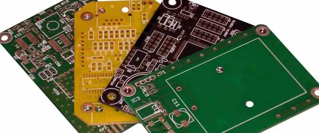
Power distribution is a critical concern when designing complex multi-board systems like servers, telecom equipment, industrial control units, etc. These systems often use large multi-layer boards or sometimes multiple interconnected boards to provide sufficient routing channels.

Implementing robust power planes within and across PCBs is key to deliver clean, stable power to all components. This article provides comprehensive guidelines on best practices for utilizing power planes in multi-board designs.

Power Plane Benefits

Dedicated power planes on PCB layers offer major benefits versus discrete power routing including:

  • Extremely low impedance power distribution network
  • Vast current capacity exceeding 10A with 1oz copper
  • Elimination of ground loops and slow power feedback
  • Prevention of switching noise coupling into signals
  • Improved voltage regulation with decoupling caps
  • Facilitates system level power sequencing

Power planes also simplify routing by avoiding tangles of power traces. Multi-board systems leverage these advantages by implementing power planes both on individual PCBs as well as across boards using backplanes or other interconnects.

Multi-Board Power Architecture

The first step is to define the system level power architecture and voltage domains. Key considerations for complex multi-board systems:

  • Number of unique voltage rails required (+5V, +12V, -12V, etc.)
  • Primary and redundant power supply modules
  • Sequence of board power up for hot-swap ability
  • Power budgeting for each board and interconnections
  • Heat dissipation needs – airflow, heatsinks
  • Fault tolerance requirements โ€“ fusing, monitoring, reporting

Architecting at the system level ensures all power requirements are fulfilled by the PCB level implementation.

Backplane Power Distribution

Backplanes or other board-to-board connectors are used to distribute power between PCBs in multi-board systems. Guidelines include:

  • Assign dedicated connector pins for each required voltage rail
  • Size pins appropriately for expected current draw
  • Ensure even pin distribution to avoid hotspots
  • Locate voltage pins adjacent to respective ground pins for local decoupling
  • Consider contact resistance for both pins and connectors
  • Incorporate redundancy for critical voltage rails
  • Use sense traces to regulate noise at board inputs
  • Add TVS diodes, fuses or polymer blocks for protection

Well designed backplane power routing avoids issues like voltage drops, noise coupling and thermal buildup across boards.

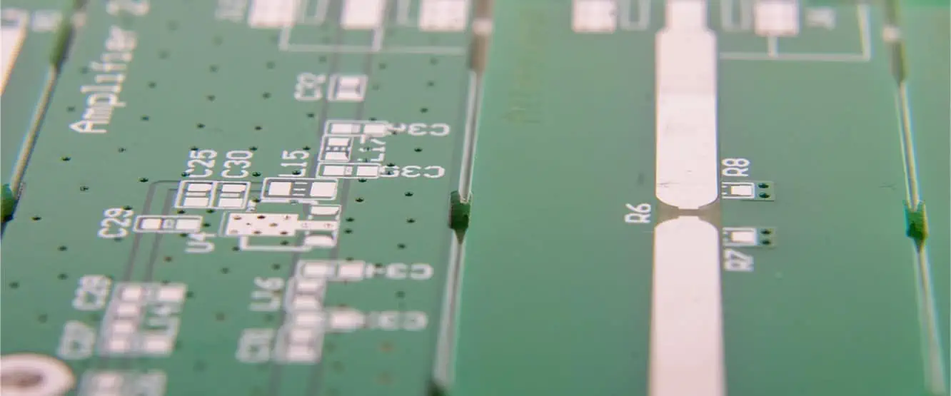
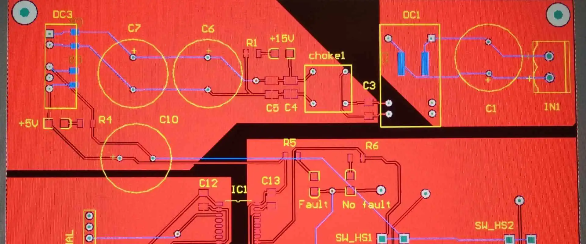
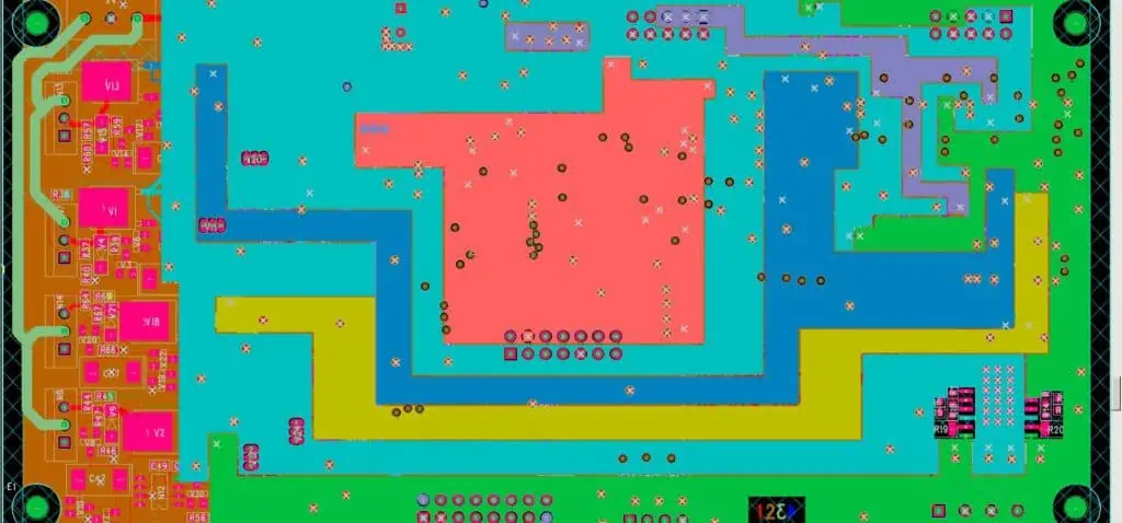
Board Level Power Planes

Within each PCB, one or more entire layers are devoted to uninterrupted power planes. Guidelines for board level power planes:

  • Assign a layer for each distinct voltage domain
  • Ensure adjacent power and ground planes for decoupling
  • Surround planes completely by guard traces or ground
  • Use thicker 2oz copper for high current applications
  • Incorporate plane splits to isolate noise sensitive circuits
  • Add multiple vias when routing signals through planes
  • Allow for thermal expansion of planes in panel design
  • Take care with plane edges near connectors and fingers

Robust power planes simplify routing while enabling stable power to all board sections.

Layer Stackup Configuration

Carefully configure the layer stackup to embed power planes optimally. Some guidelines:

  • Position ground plane adjacent to each power plane for isolation
  • Assign ground and VCC planes on inner layers adjacent to surface layers
  • Ensure surface layers are ground planes for shielding
  • Place critical signals layers closest to surface grounds
  • Use thicker power core layers when current demands are high
  • Add thin dielectric between power and ground for capacitance
  • Assign digital and analog power planes to separate layers
  • Split layers to provide embedded regulator supplies

Appropriate stackups avoid noise coupling and deliver clean localized power.

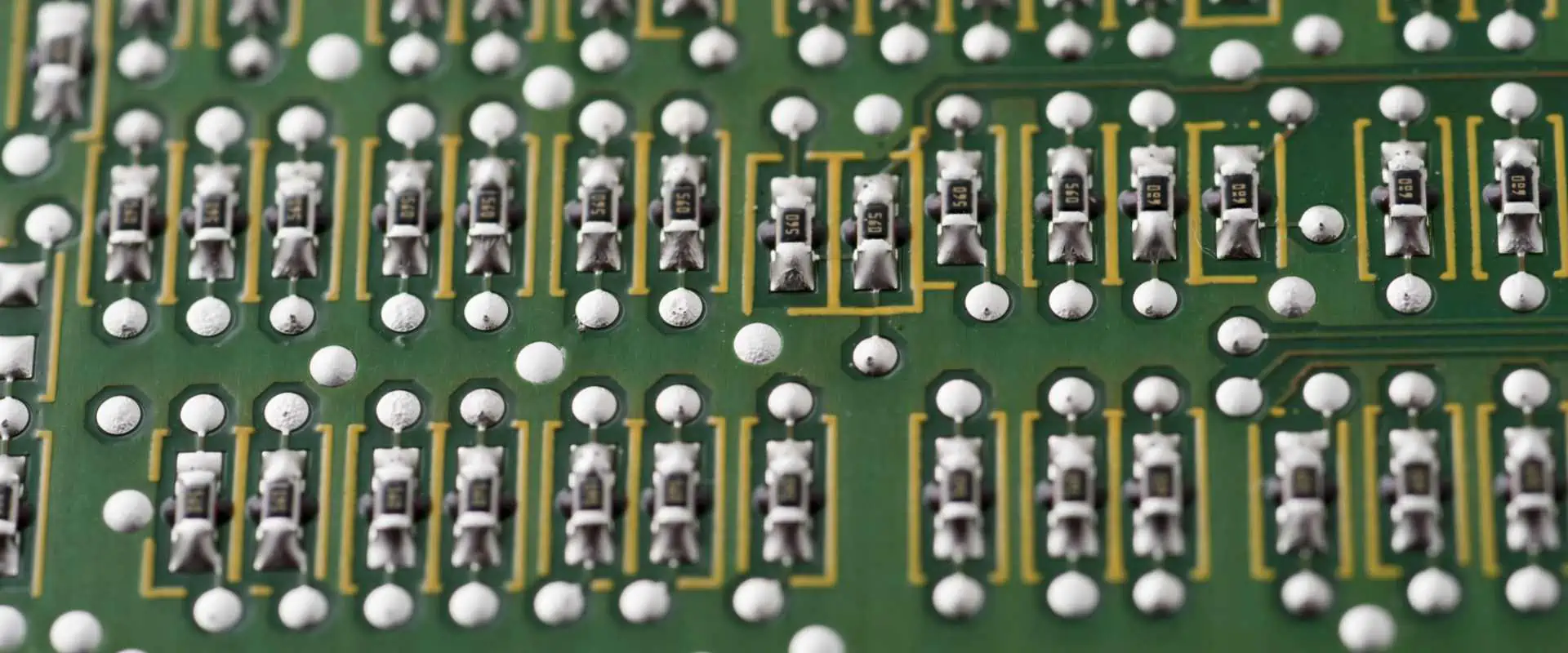
Decoupling Capacitors

Decoupling capacitors are mounted directly between power and ground planes to filter noise. Best practices include:

  • Select low ESR, X7R or NP0 capacitor technology
  • Choose appropriately sized capacitors for targeted noise frequency
  • Observe capacitor parasitics – ESL, ESR and impedance are key
  • Place caps as close to IC pins or packages as possible
  • Use staggered values for wide frequency noise suppression
  • Consider land patterns for optimal inductance and current
  • Enable capacitors in parallel for very high current applications

Sufficient high frequency decoupling is essential for stable PCB power integrity.

Polygon Pours

Polygon power fills can be used to augment planes for improved thermal relief and redundancy. Guidelines:

  • Assign polygons on inner layers adjacent to respective planes
  • Connect polygons directly to planes at multiple locations
  • Surround polygons with sufficient isolation clearance
  • Break up large polygons into smaller mesh for etch relief
  • Take care with polygon edges near fingers or connectors
  • Adjust polygon copper weight to meet current capacity
  • Keep polygon copper balanced between layers

Polygons provide supplemental power distribution with careful design.

Power Plane Splits

Power planes can be selectively split into isolated regions to prevent noise coupling when required. Some guidelines:

  • Use narrow split lines to divide plane while retaining low impedance
  • Place split lines to isolate sensitive analog sections
  • Assign individual planes for noisy digital supplies
  • Retain symmetry across plane splits for current balance
  • Bridge splits with ferrite beads when some coupled noise is acceptable
  • Decouple each split region independently
  • Add jumper connections across splits when needed

Targeted plane splits balance overall robustness with isolation needs.

Power Routing Escape Traces

Escape traces route power from the planes out to connector pins or circuit loads. Best practices:

  • Assign multiple vias when escape traces pass through ground planes
  • Place vias or stitching caps when routing over plane splits
  • Use thicker traces and minimum angles for lowest impedance
  • Avoid running other signals in parallel with power traces
  • Include power testpoints at key intersections
  • Incorporate fusing on critical power lines

Careful escape routing prevents impedance spikes and noise injection across the board.

Grounding Considerations

While focused on power, grounding interrelates and requires considerations like:

  • Minimize ground loops by routing ground returns next to signals
  • Connect all ground planes at a single point only
  • Use strategic splits in ground planes to contain return current
  • Route key signals over uninterrupted ground areas
  • Incorporate separate analog and digital ground planes
  • Assign guarded geometries around ground plane edges
  • Provide a ground return path for each power distribution branch

Robust grounding and minimal ground loops affect overall power integrity.

PDN Validation

Validate the full power distribution network (PDN) using modeling and measurement:

  • Perform impedance profiling and resonance analysis
  • Model PDN across frequency range for power noise
  • Verify impedance targets for power rail stability
  • Measure power noise directly with oscilloscope probes
  • Use VCC leakage current tests for capacitance estimation
  • Employ high frequency signal injection to locate resonances
  • Review thermal imaging under load to check for hotspots

Thorough PDN validation ensures the design meets all power integrity targets.

Design Rule Checks

4 layer pcb ground plane

Leverage design rule checks and constraints to avoid common power integrity issues:

  • Set minimum spacing between planes, traces, pads
  • Control plane edge shapes and corner radii
  • Limit the number of vias when signals cross planes
  • Set maximum trace lengths for decoupling caps
  • Require bypass caps for each power pin/terminal
  • Enforce diversified decoupling values
  • Flag missing testpoints or fusing
  • Identify unconnected plane regions or islands

Rules and constraints codify best practices to automate checking.

Summary

  • Power planes provide tremendous advantages for multi-board system PDNs.
  • Architecture the system level power distribution and sequencing first.
  • Carefully plan board power plane assignment, stackup, decoupling and routing escape traces.
  • Leverage polyethylene filled backplane pins, card edges and connectors for interconnection.
  • Validate the full PDN using modeling, measurements and thermals.

Following these guidelines delivers a robust power distribution implementation for reliable multi-board system operation.

Frequently Asked Questions

How should power be distributed between boards through backplane connectors?

Use dedicated power pins for each required voltage rail when routing connector power, with adjacent ground returns. Evenly distribute pins to avoid hotspots and use larger pin gauges or multiple pins for higher current.

What is a recommended PCB layer stackup for power integrity?

Good stackup practice is to assign ground and power planes in core layers next to signal layers. Critical signals should be next to ground planes. Place ground planes on the outer layers for shielding.

How can power plane resonance be reduced?

Strategically splitting power planes, using capacitive dielectrics between planes, and providing sufficient high frequency decoupling dampens power plane resonances. Modeling the full PDN also highlights resonant frequencies.

Why are polygon power pours used in parallel with plane layers?

Polygons provide supplemental high frequency power distribution, thermal relief for planes, and redundancy against plane breaks. But polygons have higher impedance than solid planes and introduce their own resonant effects.

What is the purpose of isolation gaps or splits within power planes?

Targeted plane splits are used to contain and isolate power noise sensitive circuitry from noisy supply regions. This prevents coupled noise while retaining robust power distribution across the overall board.

How Do You Preheat a PCB?

Preheating is an important step prior to soldering PCB assemblies. It involves raising the board temperature to a desired level before introducing solder. Proper preheating minimizes thermal stresses, improves solder joint quality, and prevents damage during hand soldering or reflow.

This article provides a comprehensive overview of PCB preheating methods, equipment, temperature profiling, and best practices. Weโ€™ll review conduction, convection, infrared, laser, and other preheat technologies along with tips for process control and optimizing results. After reading, youโ€™ll be equipped with expert knowledge on preheating PCBs for flawless soldering.

Purposes of PCB Preheating

There are several key reasons PCBs are preheated before soldering:

  • Minimizes thermal shock โ€“ Avoiding sudden temperature spikes when solder applied.
  • Reduces thermal gradients โ€“ Heat is evenly distributed to balance temps across the board.
  • Activate soldering flux โ€“ Flux needs to reach working temperature to remove oxides.
  • Drive off volatiles โ€“ Moisture and other contaminants are driven away.
  • Improve wetting โ€“ Preheating thins solder paste promoting better wetting and flow.
  • Prevent delamination โ€“ Gradually heating PCB minimizes separation of material layers.
  • Enable low-temperature solder alloys โ€“ Allows solders with tight melting ranges.

Preheat is an essential first step to soldering success. Next, letโ€™s look at preheat technologies.

PCB Preheat Methods

There are various methods used for preheating PCB assemblies:

Conduction Preheat

Uses direct contact between the PCB and a hot surface to transfer heat:

  • Heated metal plates or platens are commonly used.
  • Can be built into soldering stations or stand-alone.
  • Provides fast, even heating through conduction.
  • Limited to accessible board surfaces that can contact the plate.

Convection Preheat

Heats the board via forced air:

  • Typically uses heated air or nitrogen blown onto surfaces.
  • Enclosed convection ovens surround boards with hot air.
  • Provides general, uniform heating but slower than conduction.
  • Reaches areas not practical for contact methods.

Infrared Preheat

Leverages IR radiation to heat boards:

  • IR emitters or lamps expose boards to intense IR energy.
  • Very rapid heating achieves quick temperature ramps.
  • Line-of-sight process may cause uneven heating.
  • Risk of warping or damaging temperature sensitive components.
  • Minimal oxidizing compared to convection heating.

Laser Preheat

Focuses laser energy to rapidly heat localized areas:

  • Laser is rastered to scan heating across the PCB surface.
  • Enables precise control of heat profiles.
  • Excellent for small regions without disturbing nearby components.
  • Complex systems with optics for beam positioning and intensity control.

Thermoelectric Preheat

Uses Peltier effect for precision heating:

  • Applies current across junction of two materials to heat or cool.
  • Compact solid-state heat pumps with no moving parts.
  • Permits very precise temperature control.
  • Limited heat pumping capacity restricts area/speed.

Microwave Preheat

Dielectric heating of materials through microwave energy absorption:

  • Exposes board to tuned microwave frequencies.
  • Very rapid heating but tends to be uneven.
  • Selective heating of different materials across the board.
  • Requires microwave-transparent holding fixtures.
  • Risk of arcing with metal components.

This covers the primary preheat methods – from contact plates to lasers to microwaves. Next, weโ€™ll go over system design considerations.

PCB Preheat System Design

Several factors go into designing effective PCB preheat processes:

  • Temperature range โ€“ Match capabilities to polymer glass transition temps.
  • Heating rate โ€“ Allow ramps up to 4-5ยฐC/sec for lead-free solder.
  • Uniformity โ€“ Minimize gradients across boards for even heating.
  • Process control โ€“ Closed-loop PID algorithms for precision setpoints.
  • Atmosphere โ€“ Inerted N2 preferred over air to reduce oxidation.
  • Fixturing โ€“ Hold boards precisely while avoiding shadowing or hotspots.
  • Cooling โ€“ Active cooling can accelerate cycle times.
  • Automation โ€“ Handling robotics integrate preheat into production.

Optimized preheat systems deliver repeatable, reliable results tailored to each application need.

Solder Paste Reflow Profiling

Reflow ovens used for soldering SMT boards rely on tightly controlled preheat stages:

  • Preheat ramp โ€“ Gradual temperature increase to minimize shock stress.
  • Soak zone โ€“ Dwell time for even heating and solder paste activation.
  • Reflow peakย โ€“ Above liquidus temperature to fully melt solder.
  • Cool down โ€“ Controlled for a smooth transition and effective joint solidification.

Precisely tuned reflow profiling is key to defect-free soldering results.

Hand Soldering Preheat Guidelines

Preheating is also critical prior to hand soldering boards:

  • Use a low-power heat gun or convection heater to avoid overheating.
  • Keep nozzle moving over the area for even heating.
  • Ensure prereflow of solder paste before applying iron.
  • Let preheated joint cool briefly before soldering to avoid cracking components.
  • Shield nearby temperature-sensitive parts with kapton tape or silicone pads.

Proper preheating technique allows successful hand soldering of SMT boards without component damage.

Rework Preheat Methods

Preheating is used during PCB rework to remove and replace components:

  • Localized spot heaters target just the component area to avoid disturbing nearby parts.
  • Specialized thermal tweezers or thermodes heat individual joints rapidly.
  • Low airflow convection avoids blowing nearby components out of position.
  • Careful profiling ensures temperature stays below damage thresholds.

Strategic preheating makes PCB rework faster and safer.

Process Monitoring and Control

To achieve repeatable preheat quality, monitoring and control are vital:

  • Use thermocouples or IR sensors to provide active feedback on PCB temperature.
  • Closed-loop controllers dynamically adjust heater power to maintain setpoints.
  • Monitor gradient across the board to ensure uniform heating.
  • Placement of sensors impacts control – locate in high thermal mass areas.
  • Characterize system response to tune PID parameters for stability and speed.

Robust process control is key to consistent preheat performance.

Summary of PCB Preheat Best Practices

  • Profile temperatures and ramp rates according to solder alloy used.
  • Allow sufficient preheat soak time for uniform board temperature.
  • Shield delicate components or locally preheat large parts.
  • Use thermocouples or thermal imaging cameras to monitor heating.
  • Maintain inert nitrogen atmosphere to prevent oxidation.
  • Adjust heater power and dwells to reduce gradients across boards.
  • Validate heating efficacy through post-soldering inspection.

Following these guidelines results in ideal PCB preheating for flawless soldering.

Conclusion

Preheating is a vital first stage enabling robust PCB soldering while minimizing defects and damage. Conduction, convection, infrared radiation, lasers, and other technologies each provide unique advantages for controlled heating. By properly profiling temperatures and intelligently applying heat, high-quality solder joints are achieved. Preheating clearly plays an essential role in electronics manufacturing.

Frequently Asked Questions

How do you know what preheat temperature to use for a given PCB?

Consider the glass transition temperature of board materials along with solder paste reflow recommendations from the manufacturer. Allow a buffer of at least 50ยฐC below damage thresholds of heat-sensitive components.

What monitoring tools ensure effective preheating?

Thermocouples and IR thermal cameras are ideal for tracking PCB temperature. Closed-loop control algorithms analyze this sensor feedback to regulate heaters and achieve ideal profiles.

Is it better to use convection or conduction preheating?

Conduction preheat transfers heat faster for speed while convection provides more uniform heating across the board. Most systems apply conduction followed by convection soak to balance rapid ramps and minimizing gradients.

How does Preheat temperature affect soldering quality and reliability?

Insufficient preheat fails to properly activate flux or drive off volatiles leading to shorts or opens. Excessive temperatures can overheat components or warp boards. Tuned preheat profiles optimize joint quality.

What are some preheat considerations for large or high mass PCBs?

Slow ramp rates below 2ยฐC/sec avoid thermal shock while allowing time for heat to soak into the board. Localized or segmented heating may be required to bring up specific areas faster without scorching others.

Top 6 Best PCB Printers on Your Desk

Professional PCB fabrication traditionally required sending designs to manufacturers and waiting days or weeks to receive finished boards. However, desktop PCB printers now allow conveniently printing circuit boards in-house.

This article reviews the top 6 desktop PCB printers currently available. We will compare key specifications, capabilities, and pros/cons of each model to determine which best suits different applications and budgets. Read on to find the ideal desktop PCB printer to bring your electronics projects to life.

Overview of Desktop PCB Printers

Modern desktop PCB printers leverage various technologies to turn copper-clad plastic or ceramic substrates into functional circuit boards:

  • Mechanical Drilling โ€“ For holes and vias
  • Laser Machining โ€“ Ablates away copper
  • Milling โ€“ Uses end mills to isolate traces
  • Inkjet Printing โ€“ Deposits conductive inks
  • Photolithography โ€“ Selectively etches copper similarly to industrial processes

By combining these methods, multimodal desktop printers can fabricate detailed single or double-sided boards with fine features comparable to industrial standards. Letโ€™s examine the top models.

LPKF ProtoMat S104

The ProtoMat S104 from German firm LPKF stands as one of the most premium desktop PCB printer options:

Key Specifications

  • 10,000 rpm mechanical drill
  • 60W CO2 laser, 5.5 mil spot size
  • 4 mil milling cutter, +/- 5 mil accuracy
  • 4โ€x6โ€ max board size
  • 16 mil min trace/space

Benefits

  • Commercial quality boards
  • Very intricate cutting, drilling, and milling
  • Excellent line precision and edge quality
  • Wide material capability including flexible
  • Fiducial recognition and alignment

Drawbacks

  • High price over $18,000
  • Limited to 2 signal layers
  • Manual loading/unloading of boards

With its combination of laser micromachining, high speed drilling, and precision milling, the ProtoMat S104 produces professional multi-modal circuit boards in-house from prototype to medium volume production.

Voltera V-One

The Voltera V-One aims to bring easy, affordable PCB printing with:

Key Specifications

  • Piezoelectric inkjet for conductors
  • Single-sided boards up to 50×100 mm
  • ~200 dpi / ~127 ฮผm traces
  • 2 mil drill bits, +/- 4 mil accuracy

Benefits

  • Very low cost under $4000
  • Simple barrel ink cartridges
  • No chemical processing required
  • Easy to use touchscreen interface
  • WiFi and USB connectivity

Drawbacks

  • Slow printing speed
  • Limited to 1 layer
  • Lower resolution traces
  • Smaller board size

The V-One makes PCB prototyping accessible for education, startups, and hobbyists via hassle-free inkjet conductive trace printing combined with through-hole drilling.

Nano Dimension DragonFly LDM

This 3D printer style device uses advanced nano-particle inks to directly print PCBs:

Key Specifications

  • Proprietary silver nanoparticle ink
  • Single/double-sided PCB printing
  • 7.6 x 7.6โ€ max size
  • 2 mil printing resolution
  • 1 mil drilling resolution

Benefits

  • High conductivity metal traces
  • Multi-layer capabilities
  • Very fine print and drill resolution
  • Touch probe depth measurement
  • Fully automated operation

Drawbacks

  • High cost near $50,000
  • Limited to own conductive ink cartridges
  • Smaller build area

The DragonFly LDM produces professional quality boards through additive inkjet printing of traces combined with precise depth-controlled drilling.

Optomec Aerosol Jet 5X

Unique aerosol jetting technology distinguishes this high precision PCB printer:

Key Specifications

  • Atomized nanoparticle ink deposition
  • 5 mil min trace width
  • 1 mil drilling diameter
  • 5×5โ€ max board size
  • 2 layer capability

Benefits

  • Non-contact printing minimizes defects
  • High conductance metal inks
  • Excellent fine line capabilities
  • Dual single/double-sided printing
  • Can print non-planar surfaces

Drawbacks

  • Very high cost near $150,000
  • Limited build size area
  • Requires compressed air and N2 supply

With its high resolution and flexible printing options, the Aerosol Jet 5X excels at research-level PCB printing but has limited production utility.

BotFactory SV2

This compact printer combines inkjet printing with robotic assembly:

Key Specifications

Benefits

  • Fully automated printing through assembly
  • Tiny 1 mil holes and isolation
  • No chemical processing needed
  • Compact desktop size
  • Low cost under $5000

Drawbacks

  • Slow overall speed
  • Limited features and small size
  • Lower yield and precision

While capabilities are limited, the BotFactory SV2 provides all-in-one desktop PCB printing coupled with automated component population for rapid in-house concept prototyping.

LPKF ProtoMat E34

LPKFโ€™s entry-level circuit board plotter balances cost and quality:

Key Specifications

  • 60W CO2 laser cutting
  • 4 mil mechanical drill bits
  • +/- 8 mil precision
  • Max board size 4.7โ€ x 3.9โ€
  • Min trace/space 10 mil

Benefits

  • Reasonable ~$9000 price tag
  • Robust laser and drill performance
  • LPKFโ€™s proven mechanical engineering
  • Easy to use CAM software included
  • Upgradeable with milling/routing

Drawbacks

  • Limited feature sizes
  • Single sided only
  • Manual loading of boards

The ProtoMat E34 from LPKFโ€™s proven system provides an affordable solution for low volume, fast turnaround desktop PCB fabrication when industrial solutions are overkill.

Summary Comparison

PrinterKey ProcessesMax LayersMin. ResolutionMax Board SizePrice
LPKF ProtoMat S104Laser, Drill, Mill24 mil4โ€x6โ€$18,000
Voltera V-OneInkjet, Drill1127 ฮผm5โ€x10โ€$4000
Nano Dimension DragonFlyInkjet21 mil7.6โ€x7.6โ€$50,000
Optomec Aerosol Jet 5XAerosol Jet21 mil5โ€x5โ€$150,000
BotFactory SV2Inkjet, Dispense, Assembly21 mil4โ€x4โ€$5000
LPKF ProtoMat E34Laser, Drill110 mil4.7โ€x3.9โ€$9000

Conclusion

Desktop PCB printers grant electronics designers, engineers, and makers the ability to quickly turn their circuits into physical boards without relying on external fabrication.

From budget inkjet models to professional laser/milling systems, todayโ€™s desktop printers offer resolutions down to 1 mil and features rivaling small-scale manufacturing capabilities. As the technology continues advancing, expect wider adoption driving faster iteration in circuit design innovation.

Frequently Asked Questions

What materials can desktop PCB printers work with?

Most support common FR-4, polyimide, ceramic, and Rogers substrates. Some models allow printing flex PCBs on polyimide films. Material choice depends on requirements like flexibility, high frequency, thermal conductivity.

How many layers can desktop printers produce?

Entry-level printers generate single layer boards, while advanced models support multilayer with either double-sided printing or layer lamination. However, 4+ layers remain in the domain of full-scale PCB fabrication.

What precision and minimum feature sizes can desktop PCB printers achieve?

Leading desktop printers offer 1 mil features and accuracy rivaling industrial equipment. High-end laser, milling, and inkjet models can produce traces and spaces down to 4-5 mils. Entry-level printers support 10 mil features.

What desktop PCB printers are best for small prototypes?

For hobbyist and educational use, low-cost inkjet printers like the Voltera V-One provide an accessible starter option. For more advanced engineering prototypes, the LPKF ProtoMat E34 or BotFactory SV2 balance cost and capabilities.

What desktop printers come closest to commercial PCB production quality?

High-end laser milling hybrid printers like the LPKF ProtoMat S104 offer close to commercial board quality and feature sizes. The Nano Dimension DragonFly also produces professional grade boards through additive inkjet printing.

How to Plan PCB Projects from Design to Examples ?

Developing a new electronics product with a custom printed circuit board (PCB) involves extensive planning even before schematic entry begins. A systematic approach to planning PCB projects helps avoid costly mistakes and delays down the line.

This comprehensive guide covers how to effectively plan a PCB project end-to-end – starting from the product requirements all the way through fabrication, assembly, and testing. Read on to learn planning best practices that will set your next PCB project up for success.

Gathering Requirements

The critical first step is gathering detailed requirements that will drive the PCB design, manufacturing, and testing. Key requirements to obtain:

  • Input/output interfaces – What types of wired or wireless interfaces are needed? Common standards like USB, Ethernet, WiFi determine layout constraints.
  • Component selection – Will high power, high frequency, or space-grade components be used? Component sizes and pinouts affect PCB design.
  • Functional modes – What modes of operation are needed? This defines use cases to design and test for.
  • Performance criteria – What are the critical performance metrics like data rates, accuracy, response times, power consumption, etc?
  • Environmental factors – What environments will the product operate in – indoor/outdoor, temperature range, vibration, etc? This influences design ruggedness.
  • Compliance – What regulatory standards like UL, FCC, CE must be met? Compliance needs drive certain design and test criteria.
  • Manufacturing volume – Will this be a short prototype run or mass production? Manufacturing and inspection processes depend on volumes.
  • Budget constraints – What are cost targets for BOM, PCB fabrication, assembly, etc? Costs depend heavily on design choices.

Documenting all requirements creates a product requirements specification (PRS) that aligns cross-functional teams and ensures no gaps in planning the PCB project stages.

Selecting Components

Altium Designer 20

With requirements defined, appropriate integrated circuits, discrete semiconductors, passives, connectors, and other components can be selected.

  • Review datasheets for specifications like performance, operating ranges, packaging, pin counts, etc.
  • Prefer use of standard components that are readily available and qualified. Custom or obsolete parts often delay projects.
  • Consider environmental needs like temperature tolerance, radiation resistance, etc.
  • Model board space needed for placements based on component dimensions.
  • Check that packaging and pinouts are compatible with PCB assembly processes.
  • Minimize different component types to reduce BOM cost and complexity.

Judicious component selection while meeting technical requirements optimizes downstream PCB design.

Schematic Design

The schematic captures the circuit architecture and connectivity on paper before physical implementation.

Schematic design tips:

  • Use top-down hierarchical blocks for major subsystems. This simplifies complex designs.
  • Adhere to logical grouping and naming conventions for nets and components.
  • Include test points to facilitate hardware debugging and characterization.
  • Design with manufacturability in mind. Schematics tightly constrain PCB layout options.
  • Simulate circuit performance to verify operation before prototyping.

A complete schematic allows progressing to PCB layout with all interfaces, components, and nets logically defined.

PCB Layout

pcb layout design
pcb layout design

With the schematic complete, PCB layout can begin. This maps the logical schematic onto a physical board template.

Best practices for layout:

  • Group related components together for efficient local routing.
  • Ensure high speed paths have impedance control and isolation.
  • Include modest spare board area for last minute layout changes.
  • Follow all manufacturersโ€™ design rules for trace spacing, hole sizes, etc.
  • Design for thermal management with adequate copper heat sinks.
  • Minimize trace lengths for critical signals like clocks and high speed buses.
  • Review layouts regularly against requirements to avoid missing key features or constraints.

Careful schematic-driven PCB layout avoids costly respins due to functional or manufacturing issues.

Design Reviews

At multiple points during schematic capture and PCB layout, formal design reviews should be conducted.

Typical design reviews:

  • Requirements Review – Verify all defined requirements are properly translated into the design.
  • Schematic Review – Assess circuit correctness, manufacturability, testability.
  • Layout Review – Check form fit, tolerances, serviceability, manufacturability.
  • Safety Review – Ensure regulatory and safety standards compliance.
  • Quality Review – Confirm adherence to quality processes and documentation.

Reviews help identify issues early when they can be readily addressed, reducing costly redesigns later.

Thermal Analysis

Thermal design is a critical aspect of PCB layouts. Excessive temperatures can cause failures.

Thermal analysis process:

  • Power Maps – Estimate power dissipation for each component.
  • Heat Spreading – Ensure power planes and thermal vias distribute heat.
  • Thermal Simulation – Model temperature rises with finite element analysis.
  • Heatsinking – Add copper pads, planes, and thermal reliefs to dissipate heat.
  • Cooling – Evaluate need for fans, heat pipes, liquid cold plates, or other cooling.

Detailed thermal design improves reliability and prevents hot spots on the PCB.

Design for Manufacturing (DFM)

Embedded Hardware Engineer

PCBs must be designed not just for function but also for manufacturability.

Key DFM considerations:

  • Manufacturer Capabilities – Understand minimum trace widths, hole sizes, spacing, etc.
  • Tolerances – Account for tolerances of ยฑ10% or more in fabrication and assembly.
  • Panel Utilization – Layout board shape and placement for efficient panel use.
  • Split Planes – Avoid large copper fills which are prone to etching artifacts.
  • Test Points – Include test pads connected to nets for characterization.
  • Chamfers/Fillets – Use smooth corners on cutouts and pads for better fabrication.

Early DFM analysis avoids delays and costs of design re-spins to fix manufacturability issues.

Design for Assembly (DFA)

In parallel with DFM, assembly factors must be addressed:

  • Component Placement – Ensure they are accessible by pick-and-place machines.
  • Rotation/Orientation – Define component rotation to match assembly processes.
  • Picker Access – Account for clearances required for vacuum picker heads.
  • Adhesives – Plan locations of epoxies, tapes, staking compounds.
  • Standoffs – Include standoff locations for securing components.
  • Test Points – Provide adequate test points for in-circuit testing.

DFA techniques result in PCBs that transition smoothly from fabrication to automated assembly.

Cost Analysis

Performing cost analysis during the design process helps avoid cost overruns:

  • BOM Cost – Calculate total component cost based on volumes, sourcing options.
  • PCB Cost – Estimate board fabrication cost per units for chosen manufacturer.
  • Assembly Cost – Project expenses for population based on complexity, lead times.
  • Test Cost – Budget for test fixture development and unit testing time.
  • Compliance Cost – Factor in costs to achieve regulatory certification.
  • Tooling Cost – Account for any custom tooling like molds, jigs, fixtures.

Adjusting the design to align with target costs prevents budget surprises later.

Documentation

Maintaining up-to-date documentation is crucial for smooth PCB project execution:

  • Requirements – PRS provides the foundation for development.
  • Schematics – Fully detailed schematics essential for layout, BOMs, service.
  • PCB Drawings – Manufacturing drawings with dimensions, notes, finishes.
  • BOMs – Component lists with approved manufacturer parts and volumes.
  • Assembly Drawings – Mechanical assembly diagrams, staking drawings.
  • Test Procedures – Documented pass/fail criteria for every production test performed.

Complete documentation enables clear hand-off between teams and traceability.

Manufacturing and Assembly

With design complete, planning shifts to manufacturing and assembly.

Key planning activities:

  • Fabrication Quotes – Get quotes from 2-3 manufacturers for cost/lead time comparison.
  • Assembly Quotes – Same process for assembly houses to find best value.
  • Contract Negotiation – Finalize volume pricing and terms with chosen vendors.
  • Quality Agreements – Define defect limits, corrective actions, reliability metrics.
  • Process Qualification – Audit and certify the PCB fabrication and assembly processes.
  • Logistics – Determine shipment methods and schedules to synchronize supply chain.

Thorough planning with manufacturing partners results in quality product build at scale.

Test Strategy

Lastly, the overall test strategy must be defined:

  • Inspection Testing – Optical, x-ray inspection to check assembled boards.
  • Functional Testing – Validate operation against defined use cases.
  • Environmental Stress Testing – Test under temperature, vibration, humidity extremes per requirements.
  • Compliance Testing – Certify boards meet EMI, safety standards like CE, FCC.
  • Quality Audits – Sampling based audits to confirm manufacturing quality.
  • Test Jigs/Fixtures – Design any custom rigs needed to accurately stimulate and measure.
  • Problem Reporting – Implement tracking for yield fallout and field failures.
  • Test Documentation – Detail procedures, pass/fail criteria, equipment used.

Formal test planning reduces escaping defects and ensures robust, reliable products for customers.

Conclusion

Planning is the foundation of PCB project success. A structured approach spanning requirements gathering, design reviews, analysis, costing, documentation, manufacturing coordination, and test planning prevents problems downstream. Applying best practice project planning principles will lead to executing complex PCB programs on time and on budget.

Frequently Asked Questions

What are some key questions to ask PCB manufacturers during the planning stage?

Key questions are: capabilities and tolerances, lead times, change order rules, packaging methods, quality certifications, UL listing status, design for manufacturing (DFM) guidance, and available testing services.

What are some strategies to reduce costs during PCB projects?

Cost reduction strategies include: component standardization, dual sourcing components, value engineering design changes, negotiating vendor volume discounts, optimizing test coverage, and designing for automated assembly and inspection.

How early should compliance requirements like CE/FCC be considered?

Regulatory requirements should be analyzed right at project inception to assess needed design considerations, testing, and certification timelines which can impact schedules. Last minute certification fails can delay product release.

What are some pitfalls to avoid during requirements gathering?

Pitfalls include: unclear or conflicting requirements, leaving requirements unvalidated, excluding stakeholders, siloed teams lacking alignment, scope creep due to late additions, and failure to baseline requirements.

How can Fabrication and Assembly process capabilities be accounted for?

Engage vendors early for capabilities guidance. Perform process qualification audits. Review DFx guidelines. Define quality agreements clearly. Implement change control systems. Utilize manufacturability simulation tools during design.

What is the best PCB Prototyping Machine?

Developing new electronic products requires building multiple iterations of printed circuit board (PCB) prototypes to test and refine the design. Choosing the right PCB prototyping machine is crucial for rapidly fabricating high-quality prototypes at low costs. This guide examines the key types of PCB prototyping machines available and provides guidelines for selecting the best system based on prototyping needs.

Methods of PCB Prototyping

There are several approaches to creating PCB prototypes:

Hand Assembly

  • Manual assembly and soldering of components
  • Low volumes and iterations
  • Flexible but time consuming
  • Risk of errors and quality issues

Milling/Routing

  • CNC subtractive machining of PCB substrate
  • Flexible for design changes
  • Limited feature size and complexity
  • High equipment cost

Laser Prototyping

  • Laser ablation to selectively remove copper
  • Non-contact process preserves fine features
  • Limited line width and registration accuracy

Photochemical Etching

  • Uses photoresist and chemical etchant
  • Capable of fine features and tolerances
  • Multiple fabrication steps involved
  • Chemical handling required

Benefits of Automated Prototyping

Automated PCB prototyping machines provide important advantages over manual approaches:

  • Speed – Much faster fabrication of multiple boards
  • Repeatability – Consistent quality across prototypes
  • Precision – Tight tolerances and fine features
  • Flexibility – Quick changeover between designs
  • Reliability – Reduces human errors and defects
  • Scalability – Easily scale to higher or lower volumes
  • Productivity – Frees up skilled labor for higher value tasks

For these reasons, using an automated PCB prototyping system is recommended over DIY methods for professional prototyping.

Types of PCB Prototyping Machines

Several types of automated systems have been developed for fast PCB prototyping:

Laser Direct Imaging (LDI)

  • Uses laser to image photoresist on blank PCB panel
  • Photochemical patterning and etching follows
  • Fast imaging with no photo-tools needed
  • Limited by etching process throughput

Digital Light Processing (DLP)

  • Projector flashes UV light through mask onto PCB
  • Photoresist exposure done in minutes
  • Still requires wet etching
  • Lower cost than laser imaging

CNC Milling/Routing

  • Spinning end mill removes unwanted copper
  • Drills holes for vias and components
  • Flexible but lower precision than etching
  • Capable of limited number of layers

Inkjet Printing

  • Prints etchant-resistant ink on blank PCB
  • Subsequent etching creates conductors
  • Additive process builds up traces
  • Resolution and accuracy challenges remain

Key Machine Specifications

Important specifications to evaluate when selecting a PCB prototyping system:

  • Resolution – The minimum trace/space width that can be produced
  • Accuracy – How closely dimensions match design values
  • Repeatability – Matching quality across multiple boards
  • Throughput – Number of boards produced per hour
  • Number of Layers – Supports single, double, or multilayer boards
  • Board Size – Maximum dimensions of the PCB panel
  • Materials – Compatible board substrates and laminates
  • Line Width – Minimum/maximum trace widths supported
  • Registration – Alignment accuracy between layers
  • Solder Mask – Ability to apply solder resist coatings
  • Software – CAM tools for optimizing designs

Laser Direct Imaging Systems

laser pcb

Laser direct imaging (LDI) uses a focused laser to expose photoresist on a copper clad laminate directly based on CAD data. This gives rapid, efficient prototypes without any masks or tooling.

How LDI Works

  1. Board panel coated with photoresist
  2. UV laser scans surface, exposing photoresist patterns
  3. Developer solution removes unexposed resist
  4. Etchant textures away unwanted copper
  5. Resist stripped, followed by final finishing

Benefits of LDI:

  • Eliminates need for physical masks
  • Digital process enables fast changeovers
  • High resolution down to 25 microns
  • Suitable for circuits down to 0201 components
  • Scales efficiently from protoypes to production

Limitations of LDI:

  • Wet chemical processing limits speed
  • Initial system cost can be high
  • Requires skilled operators
  • Etching process constrains minimum trace width

Cost Considerations:

  • $50,000 to $150,000 for small systems
  • $150,000 to $400,000 for production systems
  • Lower volumes have higher board costs
  • Lower costs at mid to high production volumes

LDI provides the best combination of flexibility, precision and scalability for PCB prototyping.

Digital Light Processing Systems

Digital Light Processing (DLP) uses an LED or arc lamp projected through a photomask to expose photoresist on PCBs with speed and accuracy.

How DLP Works:

  1. PCB panel coated with photoresist
  2. Mask with transparent and opaque areas placed over panel
  3. UV light projected through mask onto panel
  4. Light hardens resist in exposed areas
  5. Developer solution removes unexposed resist
  6. Panel etched and finished as normal

Benefits of DLP:

  • Very fast exposure time in minutes
  • High resolution with 25 micron geometries
  • Small footprint equipment
  • Lower cost than laser imaging
  • Capable of soldermask coatings

Limitations of DLP:

  • Requires physical masks for each design change
  • Mask costs and lead time
  • Chemical processing creates process bottleneck
  • Limited in number of layers

Cost Considerations:

  • $30,000 to $100,000 for equipment
  • $200 to $1000 for mask tooling per design
  • $2,000 to $5,000 per mask set tooling cost
  • Lower volumes have proportionally higher costs

DLP provides a lower cost but still flexible PCB prototyping process.

CNC Milling/Routing Systems

CNC milling uses a spinning end mill to selectively remove copper from a PCB substrate to fabricate traces based on CAD designs.

How Milling Works:

  1. PCB substrate mounted to machine bed
  2. End mill moves in X-Y over panel removing copper
  3. Z-axis controls milling depth on panel
  4. After milling, PCB undergoes finishing
  5. Components populated on finished board

Benefits of Milling:

  • Direct CAD to fabrication workflow
  • No chemical processing required
  • Capable of quick turnaround
  • Design changes easily accomodated
  • Allows thick copper PCB substrates

Limitations of Milling:

  • Lower precision and tolerances
  • Limited to simpler board designs
  • High equipment capital costs
  • Produces copper dust during milling
  • Restricted to fewer layers

Cost Considerations:

  • $100,000 to $250,000 for equipment
  • $200 to $2,000 per board depending on size
  • Economical for very low volume prototyping
  • Milling time limits throughput volume

CNC milling suits low complexity PCBs in very small quantities.

Inkjet Printing Systems

Inkjet PCB printing uses inkjet heads to selectively print etchant-resistant ink onto blank copper clad boards. Subsequent etching creates the conductive traces.

How Inkjet Printing Works:

  1. Blank PCB substrate placed in system
  2. Inkjet deposits polymeric ink on panel
  3. Ink hardens to form etchant resist
  4. Etching textures away unprinted copper
  5. Resist ink removed and PCB finished

Benefits of Inkjet Printing:

  • Direct printing from CAD data
  • No tooling or masks needed
  • Additive process with no waste
  • Small equipment footprint
  • Continually improving resolution

Limitations of Inkjet Printing:

  • Still lower resolution than etching
  • Limited number of conductive ink layers
  • Restricted to lower complexity designs
  • Conductive ink challenges remain
  • Overall process slower than traditional methods

Cost Considerations:

  • $50,000 to $150,000 for small systems
  • $2,000 to $4,000 per square foot panel
  • Only economical at very low volumes
  • Cost reduces as technology matures

Inkjet PCB printing is an emerging technology still in development.

Laser Prototyping Systems

Laser prototyping uses laser ablation to directly remove copper from substrates to form circuit traces based on CAD patterns.

How Laser Prototyping Works:

  1. Blank copper clad PCB mounted in system
  2. IR laser selectively ablates unwanted copper
  3. Desired copper traces remain on PCB panel
  4. Board undergoes finishing and population
  5. Very rapid turnaround possible

Benefits of Laser Prototyping:

  • No masks, resists or chemistry needed
  • Direct non-contact copper patterning
  • Extremely fast process speed
  • High resolution down to 0.001โ€ lines

Limitations of Laser Prototyping:

  • Limited registration accuracy between layers
  • Copper smearing and debris issues
  • Restricted to simpler board designs
  • High equipment cost
  • Limited scalability

Cost Considerations:

  • $100,000 to $300,000 for equipment
  • $500 to $2,000 per board
  • Only feasible for very low volume prototyping
  • Material costs dominate overall cost

Laser prototyping suits occasional, quick-turn PCB needs.

Hybrid Prototyping Systems

pcb prototype board

Some systems combine multiple PCB fabrication technologies into a single machine for added flexibility:

Laser Imaging + Etching

  • Laser images photoresist like LDI
  • Integrated spray etching built into system
  • Reduces handling and process steps

Milling + Laser Ablation

  • Use milling for bulk copper removal
  • Laser ablation gives fine features
  • Eliminates masks and chemistry

Inkjet Printing + Etching

  • Inkjet deposits etchant resist
  • Integrated immersion etching system
  • Lower cost digital process

Hybrid machines provide versatility for prototyping needs. But integration complexity can impact costs.

Key PCB Prototyping Machine Criteria

Consider the following aspects when selecting a PCB prototyping system:

  • Volumes – Quantity of boards and iterations needed
  • Complexity – Simple double-sided or multilayer boards?
  • Resolution – Line width and space requirements
  • Materials – Substrate types and thickness
  • Iteration Speed – How quickly design changes needed
  • Technical Expertise – Operator skill level required
  • Floor Space – Size limitation for equipment
  • Budget – Total investment and per board cost targets
  • Scalability – Ability to scale up or down production

Matching the above criteria to the system specifications will identify the optimal PCB prototyping solution.

Making the Right Prototyping Machine Choice

Follow these steps to select the best PCB prototyping equipment:

  • Define prototyping requirements – quantity, complexity, precision needed
  • Determine suitable technologies – match requirements to process capabilities
  • Evaluate vendor systems – compare specifications, features, reviews
  • Assess cost considerations – equipment cost, material cost per board
  • Validate supplier qualifications – experience, customer support
  • Get hands-on demos – test machine usability and output quality
  • Consider future applications – scalability from prototyping to production

Selecting the right system will accelerate prototyping, reduce costs, and enhance electronic product development.

Frequently Asked Questions

What are some tips for operating a PCB prototyping machine?

  • Ensure proper machine setup, calibration and maintenance
  • Follow manufacturer guidelines for photoresist coating, etching, etc.
  • Use optimized board layouts and panel utilization
  • Allow sufficient tolerances for the process capabilities
  • Employ good panel handling practices to avoid damage

How many prototype boards should be fabricated?

Plan for at least 5 copies for design validation builds. Budget needing 10 copies for engineering testing. Produce 20+ copies for field evaluations. Build excess boards to allow for potential failures.

What file formats do PCB prototyping machines accept?

Gerber and Excellon formats are standard inputs. Some systems also accept PDF, DXF, SVG, HPGL, CIF, IPC-D-356A or ODB++ files.

Can PCB assembly be automated after prototyping?

Yes, automated optical inspection, solder paste deposition, component placement and reflow soldering systems enable automated assembly and higher volume production.

How are multilayer PCBs prototyped?

Systems that utilize photolithographic etching can produce multilayer boards through sequential imaging, laminating and drilling of stacked boards. Hybrid milling machines can also create multilayer boards.

Conclusion

Selecting the optimal PCB prototyping system that matches project requirements is key for fast, affordable and effective prototype builds. Laser direct imaging provides the best combination of speed, precision and flexibility for professional needs. But digital light processing, CNC milling, inkjet printing and laser ablation systems have their own advantages that suit certain applications. By analyzing production volumes, design complexity, resolution, accuracy and budget considerations, engineers can determine the ideal system to accelerate innovation and development. Robust PCB prototyping systems empower teams to rapidly test form, fit and function to successfully deliver electronic products to market.

What is PCB Racks, Holders ands Trays ?

Printed circuit boards (PCBs) are delicate and sensitive electronic components that require proper handling and storage. PCB racks, holders and trays are specifically designed to organize, protect and secure PCBs during manufacturing, assembly, testing, storage and transport. Selecting the right racking and storage solutions can safeguard PCBs against physical damage as well as electrostatic discharge. This guide provides a comprehensive overview of the different types of racks, holders and trays available for PCB applications.

PCB Racks

PCB racks provide slots or open spaces to hold multiple PCBs vertically in an organized manner. They allow easy insertion and removal of boards for access.

Rack Construction

  • Made of plastic or metal
  • Provide mounting holes to attach to worktable or enclosure
  • Some models have anti-static coating or dissipative plastics

Rack Types

  • Open frame racks – basic racks with open slots to insert PCBs
  • Enclosed racks – completely enclosed with transparent door to protect boards
  • Card cage racks – for vertically mounting PCBA cards
  • Magazine racks – allow stacking of PCBs like a magazine
  • Slotted rails – rail-based structure with slots to hold PCBs

Key Benefits

  • Organized vertical storage to systematically access each board
  • Saves benchtop space compared to laying PCBs flat
  • Allows mounting multiple PCBs of same type for production
  • Protects boards from physical damage
  • Some racks provide electrostatic discharge (ESD) protection

Applications

  • PCB storage and transport
  • Programming and testing
  • PCB assembly line workflow
  • Board burn-in testing
  • Field servicing of equipment

PCB Holders

PCB holders securely retain a single PCB to protect it during handling, testing and processing. They prevent physical stress and abrasion damage.

Holder Construction

  • Made of plastic or metal
  • Have retaining clips, screws or friction rails to lock the PCB
  • Standoffs separate PCB from base

Holder Types

  • Clip-on holders – plastic holders with clip on top to retain PCB
  • Screw-down holders – metal plates compress PCB between screws
  • Sliding holders – plastic holder with sliding rails to lock PCB
  • Pogo pin holders – provides electrical test contact with pogo pins

Key Benefits

  • Protects PCB from bending and flexing stress
  • Provides secure mounting for handling and processing
  • Compatible with soldering, cleaning and testing processes
  • Allows electrical edge connector access to PCB
  • Some holders made of anti-static materials

Applications

  • PCB hand assembly
  • Soldering and de-soldering
  • Cleaning and coating
  • In-circuit testing
  • Burn-in testing
  • Programming finished boards

PCB Trays

PCB trays provide flat protective carriers to hold PCBs horizontally without bending or warping the boards. They are used for storage, transport and PCB processing.

Tray Construction

  • Made of plastic or other polymers
  • Have divider ribs to separate each PCB
  • Anti-static conductive or dissipative polymers used

Tray Types

  • Universal trays – grid of adjustable dividers to fit various PCB sizes
  • Custom trays – molded trays fitted for specific PCB outline
  • Jedec trays – standard trays for handling ICs and chips
  • Magazine trays – stackable trays like a magazine

Key Benefits

  • Protects PCB surface from scratches
  • Prevents board warpage over time
  • Organized compartmental storage
  • Trays stackable for space efficiency
  • Anti-static material prevents ESD damage

Applications

  • PCB storage in warehouses
  • Transporting PCBs between facilities
  • Buffer storage on PCB assembly lines
  • Work-in-progress storage during manufacturing
  • Protecting finished PCB assemblies

Specifications

Key specifications to consider when selecting PCB racks, holders and trays:

Material

  • Plastic – polycarbonate, acetal resin, PTFE
  • Metal – aluminum, steel, stainless steel
  • Anti-static – dissipative or conductive polymers

PCB Capacity

  • Rack slots or holder openings for different PCB sizes
  • Trays have adjustable divider configurations

ESD Protection

  • Anti-static coatings and polymers
  • Grounding features and wrist straps

Temperature Rating

  • Withstand soldering heat up to 350ยฐC
  • Meet PCB cleaning and processing temperatures

Physical Dimensions

  • Overall outer dimensions
  • Rack slot pitch and spacing
  • Holder opening dimensions
  • Tray compartments size

Selection Criteria

Consider the following factors when selecting the optimal PCB racks, holders and trays:

PCB Size and Quantity

  • Racks and trays should fit PCB footprint
  • Determine number of PCBs to be stored

Required Protection Level

  • Open racks vs. enclosed racks vs. protective trays
  • Needed during transport, storage, or processing?

Physical Conditions

  • Environmental temperature and humidity
  • Will racks/trays encounter vibration or shock?

ESD Safeguarding

  • For handling static-sensitive boards
  • Level of ESD control needed

Mounting and Access

  • How will racks be mounted? On benchtop or enclosure?
  • Easy PCB insertion/removal required?

Budget

  • Open frame racks more economical
  • Enclosed racks and custom trays cost more

Advancements in PCB Racks and Storage

Recent improvements in PCB racking, holders and trays include:

  • Ergonomic designs: Easier handling and access to boards with slide out trays, rotating racks and adjustable working heights.
  • ESD protection: Conductive polymers, dissipative coatings and grounding features built-in.
  • Modular racks: Separate vertical slotted panels can be joined to hold different PCB sizes.
  • Smart rack monitoring: RFID tags monitor PCB locations. Sensors track environmental conditions.
  • Quick-change tooling: Faster and simpler changeover when switching PCB designs.
  • Automated racking: Robotic pick-and-place systems to insert and remove PCBs from racks and trays.

Key Benefits of Using Proper Racks and Trays

Utilizing purpose-built PCB racks, holders and trays offers important benefits:

  • Protects boards from physical damage like bending, vibration, abrasion.
  • Safeguards PCBs from ESD damage during handling and storage.
  • Eliminates tangled cables and wires hanging off loose boards.
  • More organized inventory and smoother workflow.
  • Increased PCB quality with lower defect rates.
  • Saves production time compared to improvised storage methods.
  • Safer transport between production stages without board damage.
  • Ergonomic racks reduce worker fatigue and injuries.

Storing Sensitive PCB Assemblies

PCBs with sensitive components require specialized storage:

  • Moisture-sensitive boards – Use dry storage cabinets or bags with desiccant to avoid moisture absorption.
  • Photonics PCBs – Protect photonic components from light exposure with opaque antistatic foam or dark trays.
  • High voltage boards – Prevent arcing with non-conductive trays rated for required voltage separation.
  • High frequency boards – Shielding may be needed to block external RF interference.
  • High temperature boards – Use high temperature polymers or ceramics resistant to soldering heat.

Example PCB Racking Systems

Here are some examples of complete racking systems to handle PCBs through the manufacturing process:

Storage and Transport Racking

  • Trays to store populated or bare PCBs.
  • Slotted rail racks to hold boards vertically for staging.
  • Move PCBs on carts between production areas.
  • Anti-static plastic construction.

Soldering and Washing Racks

  • Frame holder secures PCB for hand soldering.
  • Transfer boards to wash racks for cleaning process.
  • Compartment trays separate different wash batches.

Testing and Programming Racks

  • Clamshell ESD-safe holder for in-circuit testing station.
  • Indexing rack inserts boards into programming fixture.
  • Rack feeds tested boards to final packout.

Frequently Asked Questions

What are some tips for using PCB racks and trays?

  • Label rack slots and trays clearly for easy identification.
  • Use marker strips to indicate empty slots needing replenishment.
  • Insert boards gently without bending or forcing.
  • Cover unused rack openings to keep out debris and dust.
  • Lock rack casters when stationary to prevent rolling.

How can I estimate the size of rack needed?

Determine number of boards and production rate. Allow space for future requirements. A 12 or 24 slot rack is typical for small volumes. Multiples of 24 slot racks are common in production.

What design files do vendors need to create custom racks?

Supply the PCB outline drawing, preferably in dxf format. Indicate required slot pitch and quantity. List special needs like ESD protection. State expected lifetime usage.

Should racks used in wave soldering have special coatings?

Yes, racks and trays in soldering processes require high temperature coatings that withstand soldering without degrading. Fluoropolymer impregnated anodized aluminum is a common choice.

How often should I audit our PCB racks and storage?

Perform regular checks of racks and trays to ensure they remain undamaged and contaminant free. This prevents them from causing defects. Replace racks showing signs of wear. Review ESD protection and grounding.

Conclusion

PCB racks, holders and trays are critical investments to protect delicate electronics boards throughout manufacturing stages. This guide reviewed key types, specs and selection criteria to choose optimal solutions that organize and safeguard PCBs during production, storage, assembly and testing. Leveraging purpose-built racks, holders and trays improves workflow, productivity and first pass yields when dealing with large volumes of PCBs. They reduce costly board damage and ESD events. With careful selection using the principles outlined here, you can implement racks and storage that increase throughput, lower costs and deliver higher quality boards.

How to Choose the Right PCB Resistor ?

When designing printed circuit boards (PCBs), resistors are one of the most commonly used components. Choosing the right resistor for your PCB design is crucial, as it impacts performance, reliability and cost. With many types, sizes and specifications of resistors available, selecting the optimal one can get confusing. This comprehensive guide provides circuit designers a systematic approach to pick the right resistors for their PCBs.

Types of PCB Resistors

There are several types of resistors used on PCBs, each better suited for certain applications:

Carbon Film Resistors

  • Made of carbon film deposited on ceramic rod or cylindrical body
  • Low cost and widely used general purpose resistors
  • Resistance range: 1 ohm to 22 megohms
  • Tolerance: +/-5% to +/- 0.5%
  • Temperature coefficient: 250-1000 ppm/ยฐC
  • Power rating: 1/8 watt to 2 watts
  • Pros: Inexpensive, readily available
  • Cons: Lower precision, more noise

Metal Film Resistors

  • Made of thin metal film over ceramic body
  • Improved properties over carbon film
  • Resistance range: 1 ohm to 1 megohm
  • Tolerance: +/-1% to +/-0.01%
  • Temperature coefficient: +/-15 to +/-25 ppm/ยฐC
  • Power rating: 1/8 watt to 1 watt
  • Pros: Better stability and tolerance
  • Cons: More expensive than carbon film

Metal Oxide Film Resistors

  • Made of metal oxide film on ceramic substrate
  • Superior performance over metal film resistors
  • Resistance range: 10 ohms to 22 megohms
  • Tolerance: +/-0.5% to +/-0.01%
  • Temperature coefficient: +/-1 ppm/ยฐC to +/-25 ppm/ยฐC
  • Power rating: 1/8 watt to 1 watt
  • Pros: High stability, precision
  • Cons: More expensive

Wirewound Resistors

  • Made of metal wire wound around ceramic core
  • Very low resistance values possible
  • Resistance range: 0.1 ohm to 10 kohms
  • Tolerance: +/-5% to +/-0.02%
  • Temperature coefficient: 20-60 ppm/ยฐC
  • Power rating: 1 to 10 watts
  • Pros: Low resistance values, high power rating
  • Cons: Inductance effects at high frequencies

Thick and Thin Film Resistors

  • Screen printed resistive paste over substrate
  • Often used in hybrid circuits and thermal management
  • Resistance range: 1 ohm to 1 Mohms
  • Tolerance: +/-1% to +/-25%
  • Temperature coefficient: +/-50 to +/-2500 ppm/ยฐC
  • Power rating: 0.1 to 1 watt
  • Pros: Wide resistance range, low cost
  • Cons: Lower precision and stability

PCB Resistor Sizes

Resistors come in a variety of physical sizes. The major size standards are:

0402

  • Very small surface mount resistors
  • Length: 1 mm
  • Width: 0.5 mm
  • Used in high density boards

0603

  • Smaller SMD resistors
  • Length: 1.6 mm
  • Width: 0.8 mm
  • Good balance of size and power rating

0805

  • Most common SMD resistor size
  • Length: 2 mm
  • Width: 1.25 mm
  • Ease of handling and soldering

1206

  • Larger SMD resistors
  • Length: 3.2 mm
  • Width: 1.6 mm
  • Higher power handling capacity

Axial Lead Resistors

  • Through-hole resistors with leads
  • Diameter: 3 to 10 mm
  • Used for ease of prototyping and servicing

Chassis Mount Resistors

  • Through-hole power resistors
  • Used for high power applications
  • Mounted on heat sinks to dissipate heat

Key Parameters and Ratings

Beyond physical size, resistors have electrical parameters and power ratings that must be considered for PCB design:

Resistance Value

  • Measured in ohms (ฮฉ)
  • Wide range available from milliohms to gigaohms

Tolerance

  • Deviation from nominal resistance value
  • Usually +/-1%, +/-5% or +/-10% tolerance
  • Tighter tolerance increases cost

Temperature Coefficient

  • Indicates resistance change with temperature
  • Expressed in ppm/ยฐC (parts per million per ยฐC change)
  • Lower coefficient maintains stability over temperature

Power Rating

  • Maximum power a resistor can handle without overheating
  • Range from 1/8 watt for SMD up to hundreds of watts
  • Higher wattage resistors often need heat sinks

Voltage Rating

  • Maximum voltage that can be applied without arc over
  • 500V or greater voltage ratings common

How to Select the Right PCB Resistor

R=1Kฮฉ Resistor

Here are some tips for choosing the optimal resistor for your PCB design needs:

1. Determine Required Resistance Value

  • Select resistor resistance to achieve desired voltage drops and current limits in your circuit.

2. Identify Size Constraints

  • Consider board space – smaller SMD sizes needed for high density layouts.
  • Larger resistors can handle more power dissipation.

3. Choose Suitable Tolerance

  • Tighter tolerance increases accuracy and performance.
  • Looser tolerance reduces costs.

4. Check Temperature Coefficient

  • Lower temperature coefficient enhances stability in temperature changes.
  • Important for precision and reliability over a wide temperature range.

5. Verify Adequate Power Rating

  • Select resistor power rating sufficient for highest voltage/current expected.
  • Use larger resistors or add heat sinking if high power needed.

6. Check Voltage Rating

  • Ensure voltage rating exceeds maximum voltage including transients.
  • Higher voltage rating provides design headroom.

7. Select Appropriate Type

  • Carbon film – inexpensive general purpose use
  • Metal film/oxide – precision and stability
  • Wirewound – very low resistance values
  • Thick/thin film – wide resistance range

Real-World Example

Let’s go through a practical example of selecting the right resistor for a particular PCB design requirement:

Design Requirements

  1. Input voltage = 12V
  2. Load current = 500mA
  3. Need 5V output to load
  4. +/-10% voltage regulation acceptable
  5. Board space limited – 0603 size needed
  6. Operating temperature range -20ยฐC to +85ยฐC

Resistor Selection

  1. Target resistance value = (12V – 5V) / 0.5A = 14 ohms
  2. 14 ohm +/-10% tolerance needed – use 15 ohm +/-10% resistor
  3. 0603 chip size chosen for compact size
  4. Metal film resistor provides stability over temperature range
  5. 1/4 watt power rating suffices given calculated power dissipation
  6. Resistor voltage rating > 12V input

Selected Component:

  • 15 ohm +/-10% tolerance
  • 0603 size SMD chip
  • 1/4 watt metal film resistor
  • 50V voltage rating

This meets all the criteria – resistance value, tolerance, power rating, size, and voltage rating. Metal film provides precision and stability over the operating temperature range.

Resistor Marking Codes

Resistors
Resistors

Resistors use a compact coding system to label resistance and tolerance. Here are some common marking schemes:

3 or 4 Digit Code

  • First two digits – significant figures of resistance in ohms
  • Third digit – decimal multiplier (number of zeros to add)
  • Fourth digit – tolerance (1 = +/-1%, 5= +/-5%)

Examples:

  • 472 = 47 x 10^2 ohms = 4.7k ohms +/-5% tolerance
  • 8241 = 824 x 10^1 ohms = 82k ohms +/-1% tolerance

Letter Code

  • Letters indicate significant figure of resistance value
  • Following number indicates decimal multiplier

Examples:

  • R20 = R x 10^0 ohms = 0.22 ohms
  • C220 = C x 10^2 ohms = 22 pF

Color Bands

  • Colored stripes indicate resistance similarly to resistor color code
  • Additional stripe shows tolerance

To determine resistance from color bands:

  1. Read bands from left to right
  2. First two bands = first two digits
  3. Third band = decimal multiplier
  4. Fourth band = tolerance

Small Case Letters

For very low resistance values below 10 ohms, small case letters represent significant figures.

Examples:

  • 1r0 = 1 x 10^-1 ohms = 0.1 ohms
  • 75m0 = 75 x 10^-3 ohms = 75 milliohms

This covers the most common labeling schemes found on PCB resistors.

Frequently Asked Questions

How to Read Resistor by Color Code

Here are some common FAQs about choosing resistors for printed circuit boards:

What is the difference between SMD and through-hole resistors?

SMD (surface mount device) resistors are small, flat chips that are soldered directly onto the surface of PCBs. Through-hole resistors have axial leads that are inserted into holes on the board. SMDs save space while through-hole makes prototyping and servicing easier.

When should wirewound resistors be used?

Wirewound resistors are best for very low resistance values below 10 ohms where other types are not readily available. The wire winding can create inductance though, so avoid them at high frequencies.

How are resistor power ratings affected by operating temperature?

Power ratings are often derated or reduced at higher ambient temperatures. The hotter the environment, the lower the usable power rating. Resistor datasheets include power derating curves.

Can multiple resistors be used in parallel or series on a PCB?

Yes, parallel and series resistor combinations on a PCB can provide resistance values difficult to obtain with a single component. Paralleling provides lower resistance while series connections increase resistance.

How are precision thin film resistors different from other types?

Thin film resistors typically achieve much tighter tolerances down to +/-0.01%. They use special materials and manufacturing processes to create very uniform and stable resistance values for precision applications.

Conclusion

Selecting the optimal resistor requires considering multiple parameters – resistance value, tolerance, size, power rating, and temperature coefficient. Matching these specifications to your PCB’s requirements results in a design with the right precision, stability and reliability. Modern resistor materials, tight manufacturing tolerances, and anti-surge designs provide circuit designers an extensive palette for their board. By following the guidelines in this article, you can confidently choose the perfect resistor type for your next PCB design.

How Do You Use PCB Rivets?

Printed circuit boards (PCBs) provide the interconnect foundation of electronics. But PCBs arenโ€™t designed in isolation. They must interface with other components and assemblies to fully create products. An important part of enabling these mechanical connections is PCB rivets.

PCB rivets provide a robust method to attach a circuit board to chassis, enclosures, heat sinks and more. This article provides comprehensive guidance on PCB rivet usage including:

  • Rivet types and materials
  • Design considerations
  • Installation processes
  • Inspection techniques
  • Advantages over screws
  • Frequently asked questions

By covering key riveting concepts and best practices, readers will gain the knowledge to implement riveted connections that offer superior reliability and longevity.

Rivet Types for PCBs

There are two primary varieties of rivets used with printed circuit boards:

Blind Rivets

These are tubular rivets that get installed through a hole in the PCB and mating component. A blind rivet tool pulls a mandrel to flare out the rivet body securing the connection.

Solid/Drive Rivets

As the name implies, these are solid cylindrical rivets without a hollow body or mandrel. They use pressure and rotational force to create a flared joint.

Blind rivets offer easier installation while solid rivets have greater strength. Additionally, several head styles and flaring approaches provide further options:

Head Styles

  • Countersunk (flat) head
  • Oval head
  • Round head
  • Large flange head

Flaring Methods

  • Standard (cone) flare
  • Radial (trumpet) flare
  • Low-profile flare

Material choice also expands possibilities from aluminum and steel alloys to specialty options like monel and titanium.

Overall, blind rivets provide the simplest PCB attachment solution while solid rivets offer increased strength for demanding applications.

PCB Design Considerations

Several important design factors must be considered when planning to use PCB rivets:

Hole Size

The rivet diameter determines hole size. A clearance of at least 0.5 mm is ideal between the hole and rivet body.

Hole Pattern

Symmetric hole patterns provide uniform force distribution. Staggering holes diagonally can also improve shear strength.

Number of Holes

Higher shear and tensile loads require increased holes. A minimum of 4 holes is recommended with 1 hole per corner.

Hole Plating

Plated through-holes provide the most reliable riveted connection. This allows flaring against plated copper rather than base laminate.

Spacing from Holes

Riveting can cause board flexure so maintain sufficient spacing from nearby plated through holes.

Flange Spacing

Ensure room exists for rivet head height and flaring. Board and mating surface should have equal flange spacing.

Component Clearance

Allow clearance around rivets for installation access and to avoid impinging nearby components.

Mechanical Isolation

Isolate rivets from sensitive areas using cutouts or splits to prevent transmitted vibration.

Properly addressing these factors during layout ensures the PCB can be effectively riveted for maximum robustness and longevity.

Installation Processes

With the board designed, letโ€™s look at best practices for installation:

Hole Preparation

Prepare holes by removing burrs and clearing debris. This allows rivets to properly seat against hole walls.

Component Staging

Stage the PCB and mating component(s) together in the assembly configuration and rivet joints aligned. Clamping or fixturing helps alignment during installation.

Rivet Insertion

Insert rivets into each prepared hole. Rivet heads should seat flat against the PCB and mating component flanges.

Installation Tool Setup

Select a rivet hand tool, pneumatic tool, or hydraulic pull tool matched to the rivet size and access requirements. Adjust any controls like pressure or stroke length.

Flaring

Activate the tool to flair the rivet. For blind rivets, this pulls the mandrel to expand the body. Solid rivets use pressure and rotation to flare outward.

Mandrel Removal

For blind rivets, use flush cutters to shear off and remove the leftover mandrel flush with the rivet head.

Inspection

Visually inspect each rivet joint to ensure sufficient flaring and head seating. Repair any insufficient connections before completing assembly.

Proper tool selection, preparation, and flaring technique result in strong, reliable through-hole rivet bonds.

Inspection Methods

Inspection of rivet joints helps verify quality and strength. Some key inspection aspects:

Flaring Shape

  • Flare should reach close to hole edges without exceeding
  • Flare should have smooth, symmetric shape

Head Seating

  • Head should sit flat against flange surface
  • No gaps between flange and head

Hole Filling

  • Flare should fill at least 80% of hole area
  • Little unfilled space visible around rivet body

Board Condition

  • Check for lifted copper pads, cracks, or delamination
  • Indicates excess force or stress

Both visual inspection and tools like x-ray imaging can provide insight into internal rivet structure. Testing sample rivets to failure determines shear and tensile strength.

Advantages vs. Screws

Letโ€™s also discuss some benefits of using PCB rivets compared to screws:

Vibration Resistance

Rivets form a fixed, non-moving joint. This resists loosening over time from vibration. Screws are susceptible to backing out.

Assembly Speed Rivet installation is faster than driving screws. Large volumes of rivets can be quickly installed.

Reduced Components

Rivets donโ€™t require extra components like washers, screw threads, and nuts. The rivet body provides an all-in-one fastener.

Material Options

Rivets come in more materials than screws such as titanium. This provides flexibility for specialized applications.

Lower Profile

Rivet heads can be less protrusive than screws. Flatter profiles are possible.

Improved Appearance

For external applications, rivets offer a more finished look compared to exposed screw heads.

The permanence and tight fit of rivets makes them ideal for PCB connections under vibration and longevity requirements.

Frequently Asked Questions

Some common questions that arise around PCB rivets:

How are hole size and rivet size matched?

Generally select a rivet shank 0.1-0.3 mm smaller than the hole. The flare fills the remaining space to create a tight assembly.

What tools are needed for installation?

Blind rivets require only simple handheld or pneumatic pull tools. Solid rivets need more advanced rotary-pull tools for best connections.

What force is needed to shear rivet joints?

Well installed rivets offer over 1,000 KgF shear strength and close to 2,000 KgF of tensile strength depending on the rivet size and material.

Can repetitive assembly/disassembly damage rivet holes?

Yes, hole plating and structure can degrade with repeated rivet removal and re-work. Permanent press-fit pins may be better for field replacement needs.

How many boards can be riveted before re-tooling is needed?

On the order of 500 rivet cycles can be achieved before typical hand tools require adjustment, cleaning, or replacement of worn parts.

In summary, matching rivet type and geometry for the design needs is key for achieving robust, reliable PCB connections.

Conclusion

Riveting provides a strong, vibration-resistant means of mechanically attaching PCBs. The versatility of rivet styles and materials allows an ideal solution to be tailored for the design requirements. With careful hole layout and quality installation practices, riveted connections outperform traditional screw fastening.

While requiring some upfront planning, the long term benefits are significant. The permanence of rivets prevents loosening while their simplicity speeds assembly. Riveting improves product life, assures proper grounding, and enhances aesthetics.

So for your next design needing robust board mounting, look beyond just screws. The wide capabilities of PCB riveting make it a compelling alternative for connectors, EMI shielding, board stacking, and other attachments. With the guidelines presented here, youโ€™ll be ready to implement riveted connections that maximize reliability.

What is PCB Scans Service ?

Printed circuit boards (PCBs) are at the heart of electronics. As products become more advanced, PCBs grow more complex. This complexity makes verifying that a PCB matches the original design intent increasingly critical. PCB scans help provide that verification through detailed inspection and analysis.

PCB scans offer a comprehensive way to validate board fabrication quality. This article will explore what PCB scans services encompass including:

  • The different types of scans
  • Typical scan deliverables
  • How scan data gets analyzed
  • Use cases showing value of scans
  • Options for implementing scanning
  • Frequently asked questions

Read on to understand how utilizing scans can improve quality across the PCB development and production cycle.

Types of PCB Scans

There are a few core types of scans used to validate PCB fabrication:

Optical Scans

These use cameras and image processing software to capture highly detailed images of a PCB. The scanned images enable inspection of trace width, spacing, mask alignment, and more. 2D optical scans provide a layer-by-layer view while 3D scans can create models of the entire board.

X-Ray Scans

X-ray scanning reveals internal PCB structure. This allows verification of layer alignment, voids, and defects within the board that are invisible from the outside.

Automated Optical Inspection (AOI)

AOI systems use cameras, lighting, and software algorithms to automatically flag defects on a PCB. This provides fast pass/fail verification to complement manual optical inspection.

Electrical Testing

Testing functionality electrically through in-circuit or flying probe testing. Confirms boards operate as designed rather than just verifying physical traits.

Cross-Sectioning

Physically cutting a sample to expose internals for measurements under a microscope. Most accurate way to assess plating thickness and layer alignment.

These different scans provide complementary views into PCB quality. Optical scans deliver detailed imagery while x-ray and cross-sectioning reveal the boardโ€™s internal structure. AOI and electrical testing provide automated defect detection. Typical scan services utilize a combination of these techniques tailored to the specific board and application requirements.

Scan Deliverables

PCB scan services provide a range of detailed deliverables. These help document quality and assist further analysis. Typical deliverables include:

High Resolution Board Images

  • Layer-by-layer photos showing fine details
  • Captured under precision lighting
  • Multiple angles provide complete view

Measurement Annotations

  • Board images with measurement callouts
  • Critical attributes like trace width documented
  • Pass/fail status noted based on specified tolerances

Layer Composite Images

  • Overlays images from multiple layers
  • Used to assess alignment and stackup

3D Board Models

  • Photorealistic 3D model of assembled board
  • Enables inspection from any angle
  • Zoom into component-level detail

Automated Inspection Data

  • Results from AOI inspection
  • Log of fails and process metrics
  • Used for process control and optimization

Cross-Section Images

  • Detailed photos of board cross-section
  • Reveals plating quality and thickness
  • Assesses inner layer alignment

These deliverables provide full visibility into the as-built state of PCBs. They serve as an important quality benchmark and enable further analysis.

Scan Data Analysis

The scan deliverables provide a wealth of data to analyze fabrication quality. A few examples of how this data gets used:

Dimensional Analysis

The photorealistic board images support precise dimensional measurement of features like trace width and spacing. This verifies all aspects match the original design files.

Layer Alignment Assessment

Layer composites and cross-sections reveal alignment between layers. This includes registration between layers and inner layer skew.

Plating and Etching Analysis

Plating quality and etching characteristics can be inferred from images. For example, uneven plating or over-etching of traces.

Solder Mask Inspection

Mask dimensions relative to copper features are measured. Images reveal solder mask registration errors and insufficient openings.

Voiding and Defect Detection

X-ray scans combined with cross-sectioning uncover voids, gaps, and other defects in the PCB substrate

Process Capability Analysis

Automated inspection data allows statistical process control metrics to be calculated. This reveals fabrication consistency.

These examples demonstrate the breadth of insights possible from scan data. It provides vital feedback for continually improving manufacturing processes.

Use Cases Showing Value of Scans

Now that weโ€™ve explored the scan types and analysis performed, letโ€™s look at a few examples showing the value scans offer across the PCB production cycle:

Research & Development

During R&D, scans help accelerate prototyping by providing detailed validation of new designs and processes. Images allow quick comparison between design and fabricated board.

Pre-Production

Before full production, scans verify that fabrication processes meet specifications consistently across pilot builds. Issues can be corrected earlier.

New Supplier Qualification

When qualifying a new fabrication supplier, scans supply quantitative data about their capabilities relative to requirements.

Batch Quality Monitoring

Periodic scans during production provide ongoing process control. Scan data can detect deviations so corrections can be made before volume production.

Design Issue Diagnosis

If functional issues arise, scans provide detailed physical data to help determine the root cause. For example, whether a short is from a PCB flaw or faulty assembly.

Counterfeit Screening

For products with high counterfeit risk, scans supply physical forensic data to identify boards not produced by approved suppliers.

These examples highlight the benefits of PCB scans during prototyping, ramp-up, and volume production. The data aids issue diagnosis, process control, and quality assurance.

Options for Implementing Scanning

PCB-Copy

There are a few options available for implementing PCB scan services:

In-House Scanning

Scanning can be brought fully in-house by investing in equipment such as automated inspection, x-ray, and cross-sectioning tools. Offers full control but requires significant capital expenditure.

Outsource to Specialized Provider

Many companies offer outsourced scanning services. These providers supply the equipment, expertise, and capacity needed for on-demand scanning.

Hybrid Approach

Some capabilities like AOI can be brought in-house while specialized techniques like x-ray remain outsourced. This balances control, cost, and flexibility.

Supplier Scanning

Require PCB suppliers to provide scan data as part of fabrication services. Shifts burden to supplier but scan access may be limited.

The right implementation depends on budget, internal expertise, quantity of scans, and quality control approach. As volumes increase, bringing more capabilities in-house makes sense for full control and traceability.

Frequently Asked Questions

A few common questions arise around PCB scan services:

What does PCB scanning typically cost?

Outsourced scan costs range from $250 – $1000 depending on complexity, scan types, and deliverables. Bringing in-house requires equipment investments from tens to hundreds of thousands of dollars.

How long does it take to scan a board?

High resolution optical scans can be completed in under a day excluding time for delivery and analysis. Automated inspection offers even faster turnaround. More complex analysis like cross-sectioning takes longer.

Is scanned data proprietary?

If outsourcing, providers typically retain rights to scan techniques but board data belongs to the customer. Data privacy should be ensured.

What defect detection resolution is possible?

Inspection can reliably detect defects down to 2-5 microns. Smaller defects may be visible but cannot be consistently distinguished from normal variations.

How many boards are needed for sampling?

5-10 samples from a batch provides good insight into quality variation. Complex boards may need more. Both pilot and volume production should be evaluated.

In summary, PCB scans deliver detailed physical validation while questions of cost, time, and implementation depend on specific needs. When used appropriately, scanning adds significant quality assurance value.

Conclusion

PCB scan services provide invaluable verification of board fabrication quality. The variety of scans available equip engineers with multidimensional data to validate PCBs relative to design specifications. Photorealistic imagery combined with automated inspection and cross-section analysis ensure boards meet requirements.

Scans identify issues early when corrections are lower cost. They also provide process feedback to continually refine manufacturing. As PCB technologies advance, scanning offers the level of precision needed to achieve quality and reliability targets. While adding cost, the value realized across prototyping, pre-production, and volume manufacturing outweighs investments. By proactively using scans instead of reacting after functional failures, organizations gain higher PCB quality along with improved time-to-market and lower risk.

What is PCB Scoring: Tools, Tolerance and Guideness

Printed circuit boards (PCBs) are an integral part of most electronic devices. They provide the foundation on which components are mounted and connected. However, not all PCBs are created equal. The quality and reliability of a PCB depends greatly on the fabrication process and tolerances used.

One way to assess PCB quality is through scoring. PCB scoring involves analyzing specific attributes like track width, spacing, hole size, etc. to determine how closely the PCB matches the original design specifications. Tighter tolerances generally indicate a higher quality PCB.

This article will provide an in-depth look at PCB scoring. It covers:

  • The importance of PCB scoring
  • Common PCB attributes analyzed
  • Scoring tools and methods
  • Typical tolerances and guidance values
  • How scoring data is used
  • Frequently asked questions

Understanding PCB scoring provides vital insight into board quality. Read on to learn more about this important process.

The Importance of PCB Scoring

PCB scoring provides a quantitative way to assess the fabrication quality and consistency of printed circuit boards. It helps answer the question: How closely does my board match the original design?

Tight tolerances are critical for several reasons:

Reliability

Boards with tight tolerances are more reliable over time. Features like thin tracks and spaces see higher failure rates as tolerances widen. Tighter tolerances minimize risks like short circuits.

Assembly Yield

The assembly process is much easier when PCB tolerances are tight. Wider variances make it challenging to properly place and solder components. This lowers yields and increases rework.

Performance

Electrical performance depends on tight layout tolerances. Skews in track widths or spacings can alter impedance, crosstalk, and other parameters. This degrades signal integrity.

Interchangeability

Consistent PCB quality ensures interchangeability. If tolerances vary widely, swapping boards or components may be difficult. This can limit repair options.

Detection of Process Issues

Scoring provides vital feedback on fabrication processes. Trends in the data can reveal issues like miscalibration or tool wear. This allows for targeted process improvements.

In summary, PCB scoring provides key insights into quality and consistency. This allows fabrication issues to be identified and addressed early. Tight tolerances are essential for reliable, high-performance circuit boards.

Common PCB Attributes Analyzed

Many important PCB attributes are commonly analyzed during scoring. This includes physical features like track widths, hole sizes, spacings, and more. Here are some of the key parameters typically checked:

Track Widths

The width of copper tracks on the PCB. Good control ensures impedance tolerances are met.

Track Spacing

The space or isolation between adjacent copper tracks. Tight control prevents short circuits.

Hole Sizes

The diameter of drilled holes used for component leads and vias. This affects fit with component leads.

Annular Rings

The copper ring around a drilled hole. Sufficient width is needed for hole wall integrity.

Mask Alignment

The alignment of solder mask to copper features. Misalignment can impact soldering processes.

Copper Thickness

The deposited copper thickness after plating. Affects track conductivity and current capacity.

Registration

Alignment of layers to each other. Important for ensuring reliable interlayer connections.

Etchback

Reduction of copper thickness from etching. Can impact track resistance if excessive.

Solder Mask Cure

The degree of solder mask curing. Insufficient curing can cause masking issues.

This covers some of the most common attributes analyzed. However, other parameters like via tents, beveling, etc. may also be checked as needed. The specific attributes scored depend on the PCB design and its performance requirements.

Scoring Tools and Methods

v-cut machine
V-cut machine

Now that weโ€™ve covered which attributes require analysis, letโ€™s look at how scoring is actually performed. There are a few core methods and tools used:

Optical Measurement

This uses microscopy and image analysis software to take measurements. It offers high accuracy but can be relatively slow.

Automated Optical Inspection (AOI)

AOI systems use cameras to automatically measure PCB features. Algorithms analyze the images to check tolerances. Very fast but capital investment is high.

Electrical Testing

Certain attributes like track width can be indirectly measured electrically. Simple and fast but not as precise as optical methods.

Cross-Sectioning

Cuts a small PCB sample and uses microscopy to measure internal features like plating thickness. Very accurate but sample preparation is required.

Laser/Camera Scanning

Non-contact 3D scanning generates a detailed model for inspection in CAD software. No sample prep but requires expensive equipment.

In most cases, a combination of methods is used. Optical tools provide detailed measurement capability while electrical and image processing techniques enable fast automated batch testing.

Advanced data analysis is also utilized. Statistical methods are applied to scoring results to characterize fabrication capability over many boards and builds. This allows fine-grained process control.

Typical Tolerances and Guidance Values

To interpret PCB scoring results, we need to know the target tolerances for each attribute. While specific acceptable variances depend heavily on the design, here are some typical guidance values:

FeatureTolerance
Track Widthยฑ10%
Track Spacingยฑ10%
Hole Diameterยฑ10%
Annular RingNo less than 5 mil excess ring
Mask Alignmentยฑ3 mil
Copper Thicknessยฑ10%
Registrationยฑ3 mil
EtchbackNo more than 2 mil reduction
Solder Mask Cure80% minimum cured

Anything outside the tolerance would be flagged for further investigation. However, tighter specifications are often required for high density or high frequency layouts.

Itโ€™s also important to analyze the distribution of the measurements, not just the min/max values. Tight clustering close to the nominal values indicates solid process control. High variance points to potential issues.

Benchmarking against industry standards like IPC-A-600 provides further guidance. But ultimately, tolerance settings must align with the specific needs of the design and application.

How Scoring Data is Used

V-Groove PCB

PCB scoring provides key data to assess and control fabrication processes. There are a few primary ways the results are used:

Analyze Manufacturing Consistency

Firstly, scoring provides a clear view of manufacturing consistency. Tight, consistent results across fabrication runs indicate good process control. High variability would dictate tuning is required.

Identify Process Issues

The data can pinpoint specific problem areas needing attention. For example, track width variances may point to resolution issues with imaging processes. Scoring helps target root causes.

Qualify and Compare Suppliers

Scoring is invaluable when qualifying new suppliers or comparing vendors. It provides an objective benchmark of their capabilities based on measurable results.

Feed Back into Design Rules

The results should be fed back into design rules and stackup requirements. For example, scoring may show that a certain track spacing is prone to shorts and spacing rules should be adjusted.

Monitor Trends and Capability

Statistical techniques can track scoring trends over time to detect subtle shifts. This allows the fabrication process capability to be characterized and optimized.

In summary, scoring provides vitally important feedback. The data drives continual improvement through refined design rules, process enhancements, and objective supplier assessments.

Frequently Asked Questions

There are a few common questions that arise around PCB scoring:

Q: How many boards need to be scored to provide meaningful data?

A: Typically 5-10 boards provides a reasonable sample size. More may be needed for very high volume designs. Both pilot builds and production runs should be assessed.

Q: Does scoring increase PCB fabrication time?

A: Slightly, but the benefits far outweigh a small time penalty. Today’s automated optical tools provide very rapid scoring.

Q: Can every design parameter be realistically scored?

A: Not always – scoring focuses on features prone to high process variation or sensitivity. But parameters can be tailored to each design.

Q: Is scoring expensive?

A: The material costs are low since it requires just a few PCB samples. But advanced measurement tools do require capital investment from the manufacturer.

Q: Can scoring data be provided to customers?

A: Yes, many suppliers provide detailed scoring reports to customers to showcase quality. However, some view the data as proprietary.

In summary, PCB scoring provides vital feedback that improves quality, consistency, and reliability. While adding some time and cost, the benefits for fabrication process control are enormous. When combined with fundamental process monitoring like IPC-A-600, scoring accelerates improvements through real-time quantitative data.

Conclusion

PCB scoring offers a data-driven approach for optimizing fabrication quality and consistency. By leveraging measurement tools and statistical techniques, scoring generates actionable insights into the manufacturing process. Tight tolerances are verified, issues are identified, and improvements can be tracked.

While sampling does add cost, the system-level view provided by scoring data is invaluable. It provides fundamental feedback needed to achieve reliable, high performing PCBs that match the original design intent. With the growing complexity of todayโ€™s electronics, scoring is now an indispensable tool for staying ahead of quality issues before they derail projects and timelines.