Introduction
In the world of high-frequency circuit design, minimizing signal loss is crucial for achieving optimal performance. One of the key factors that designers must consider is insertion loss, which refers to the loss of signal power that occurs when a component is inserted into a transmission line or signal path. Rogers Corporation’s RO4000 LoPro laminates have gained popularity in recent years due to their ability to significantly improve insertion loss in high-frequency applications. This article will delve into the intricacies of insertion loss, explore the unique properties of RO4000 LoPro laminates, and provide practical strategies for leveraging these materials to enhance your circuit designs.

Understanding Insertion Loss
What is Insertion Loss?
Insertion loss is a measure of the reduction in transmitted signal power due to the insertion of a device in a transmission line. It is typically expressed in decibels (dB) and is a critical parameter in high-frequency circuit design. The lower the insertion loss, the better the signal integrity and overall system performance.
Factors Affecting Insertion Loss
Several factors contribute to insertion loss in high-frequency circuits:
- Dielectric loss
- Conductor loss
- Radiation loss
- Surface roughness
- Impedance mismatches
Understanding these factors is essential for developing strategies to minimize insertion loss and improve circuit performance.
Introduction to RO4000 LoPro Laminates
What are RO4000 LoPro Laminates?
RO4000 LoPro laminates are a family of high-performance circuit materials developed by Rogers Corporation. These laminates are designed specifically for high-frequency applications where low insertion loss is critical. The “LoPro” designation refers to the low-profile copper foil used in these materials, which contributes to their superior performance characteristics.
Key Features of RO4000 LoPro Laminates
RO4000 LoPro laminates offer several advantages for high-frequency circuit design:
- Low dielectric constant (Dk)
- Low dissipation factor (Df)
- Tight Dk and thickness tolerances
- Low profile copper foil
- Excellent thermal stability
- Good dimensional stability
These features combine to make RO4000 LoPro laminates an excellent choice for applications requiring low insertion loss and high signal integrity.
Strategies for Improving Insertion Loss with RO4000 LoPro Laminates
Optimizing Dielectric Properties
One of the primary ways to improve insertion loss is by optimizing the dielectric properties of the substrate material. RO4000 LoPro laminates excel in this area due to their low dielectric constant (Dk) and low dissipation factor (Df).
Low Dielectric Constant (Dk)
The dielectric constant of a material affects the speed at which electromagnetic waves propagate through it. A lower Dk results in faster signal propagation and reduced signal delay. RO4000 LoPro laminates typically have a Dk in the range of 3.3 to 3.55 (depending on the specific grade), which is relatively low compared to many other PCB materials.
To leverage this property:
- Choose the appropriate RO4000 LoPro grade based on your specific Dk requirements.
- Design your transmission lines with the correct impedance, taking into account the low Dk of the material.
- Consider using thinner substrates to further reduce the effect of dielectric loss.
Low Dissipation Factor (Df)
The dissipation factor, also known as the loss tangent, is a measure of the energy lost in the dielectric material. A lower Df translates to lower dielectric losses and, consequently, lower insertion loss. RO4000 LoPro laminates boast impressively low Df values, typically ranging from 0.0025 to 0.0037 at 10 GHz.
To take advantage of the low Df:
- Select the RO4000 LoPro grade with the lowest Df that meets your other design requirements.
- Design your circuits to operate at frequencies where the material’s Df is lowest.
- Minimize the length of high-frequency signal paths to reduce the cumulative effect of dielectric losses.
Leveraging Low-Profile Copper Foil
One of the defining features of RO4000 LoPro laminates is their use of low-profile copper foil. This specially treated copper foil has a much smoother surface than standard electro-deposited (ED) copper, which significantly reduces conductor losses due to the skin effect at high frequencies.
Reduced Surface Roughness
Surface roughness contributes to insertion loss by increasing the effective path length that signals must travel and by causing small-scale reflections. The low-profile copper foil used in RO4000 LoPro laminates has a typical RMS (root mean square) roughness of less than 0.4 μm, compared to 1.8-2.8 μm for standard ED copper.
To maximize the benefits of low-profile copper:
- Design your transmission lines to take full advantage of the smooth copper surface.
- Consider using wider traces for critical high-frequency paths to further reduce conductor losses.
- Implement proper copper plating techniques during PCB fabrication to maintain the low surface roughness.
Skin Effect Mitigation
The skin effect causes current to flow primarily near the surface of a conductor at high frequencies, effectively increasing the resistance of the conductor. The smooth surface of low-profile copper helps mitigate this effect by reducing the “effective” surface area through which the current must flow.
To further mitigate the skin effect:
- Use wider traces for high-frequency signals to increase the effective conductor cross-section.
- Consider using copper coin technology for areas requiring enhanced thermal management or lower resistance.
- Implement proper stackup design to ensure optimal current distribution in multilayer designs.
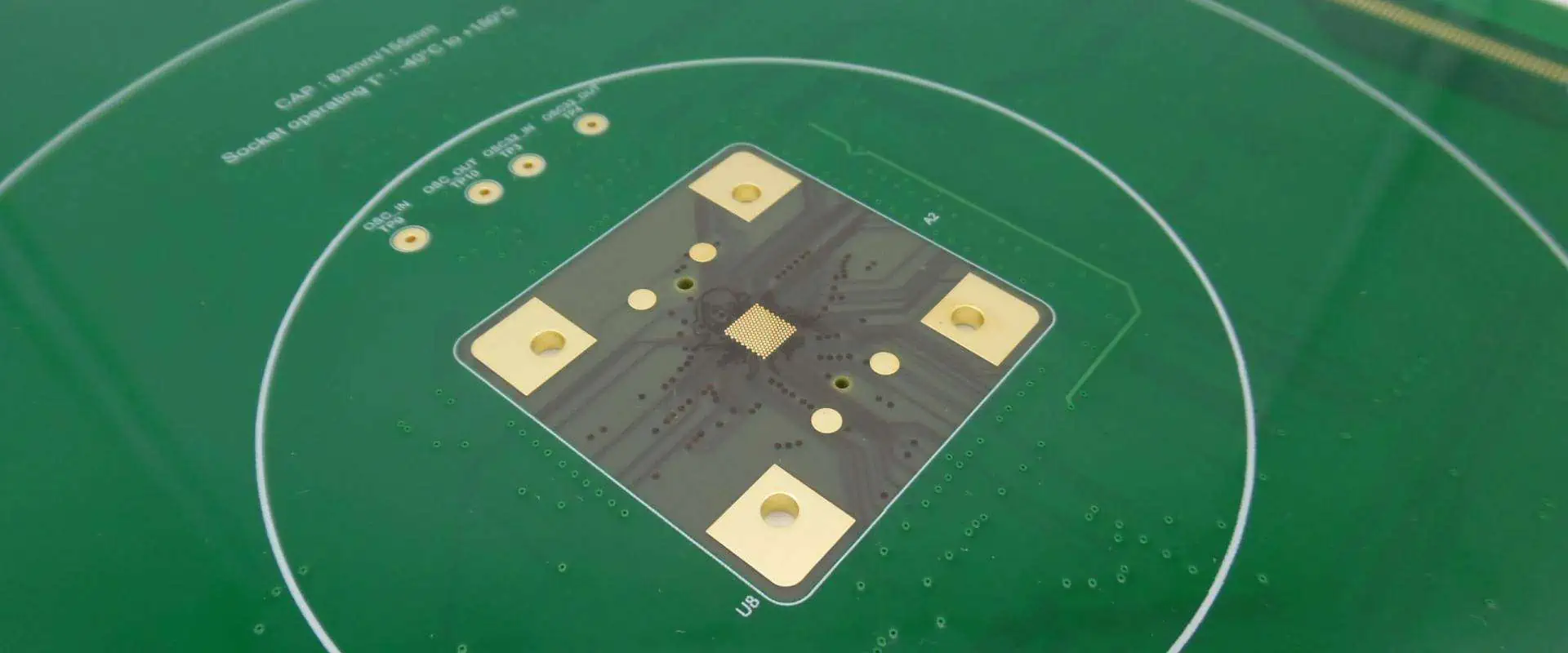
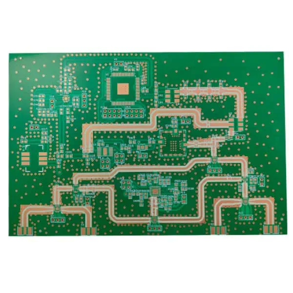
Optimizing PCB Design and Layout
While the material properties of RO4000 LoPro laminates provide an excellent foundation for low insertion loss, proper PCB design and layout techniques are crucial for maximizing their benefits.

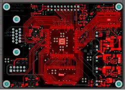
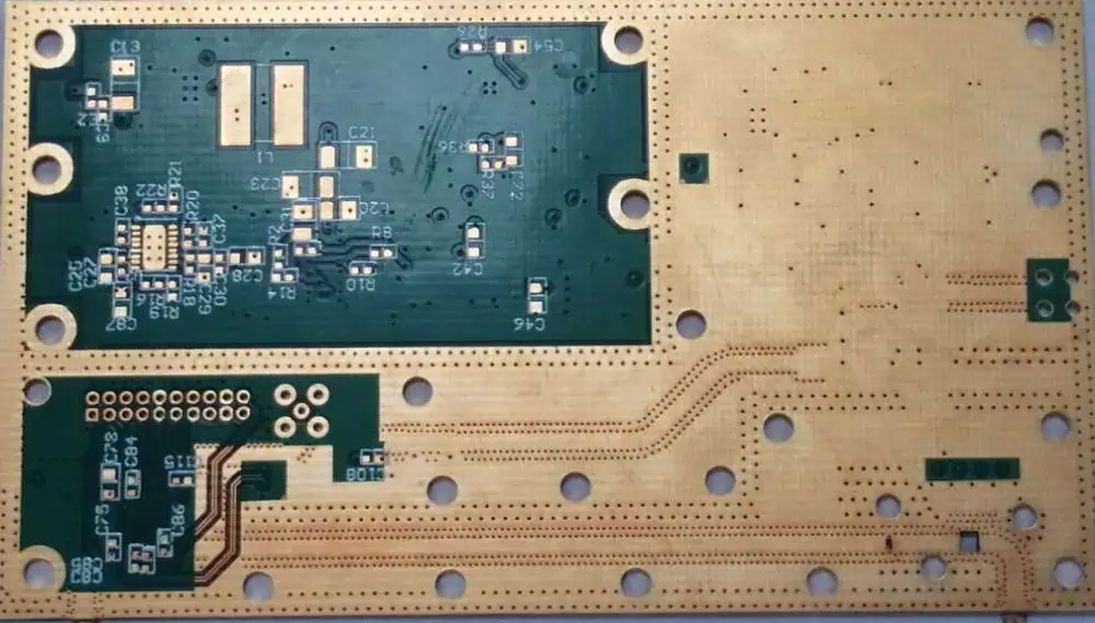
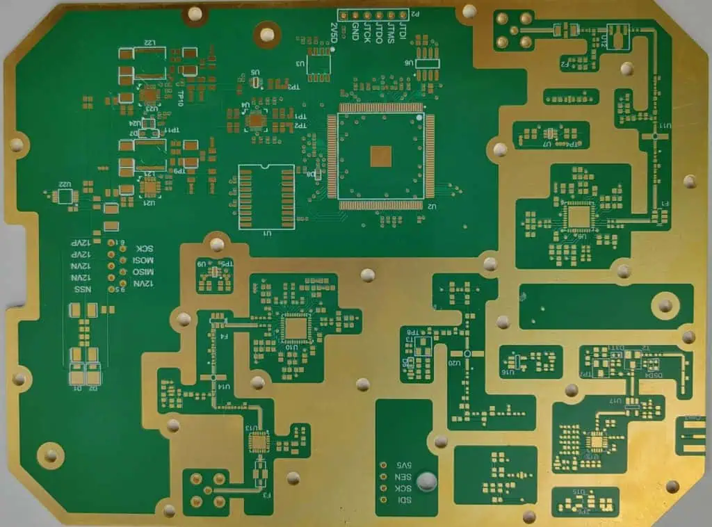
RayMing 4 Layer 1.6mm Rogers 4003 Circuit Board
Rogers 4003 is a ceramic-filled, woven glass reinforced hydrocarbon/ceramic laminate material specifically engineered for high-frequency and high-speed digital applications
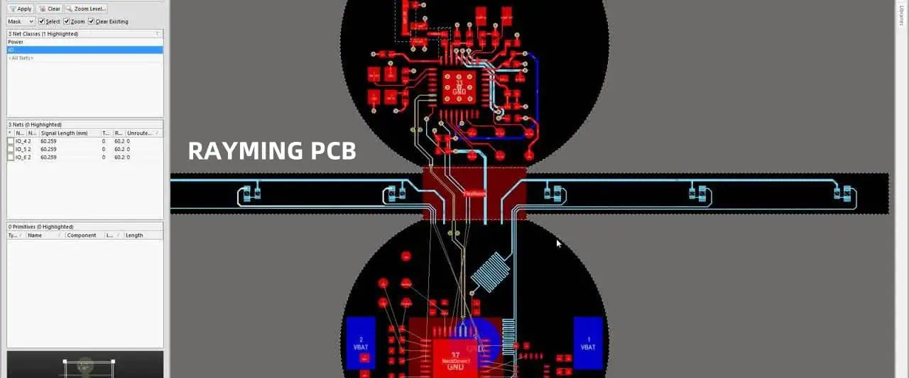
Transmission Line Design
Proper transmission line design is essential for minimizing insertion loss and maintaining signal integrity. When working with RO4000 LoPro laminates:
- Use appropriate transmission line structures (e.g., microstrip, stripline) based on your application requirements.
- Carefully calculate and maintain the correct impedance throughout the signal path.
- Minimize discontinuities and transitions in the transmission lines.
- Consider using tapered line transitions to reduce reflections at impedance changes.
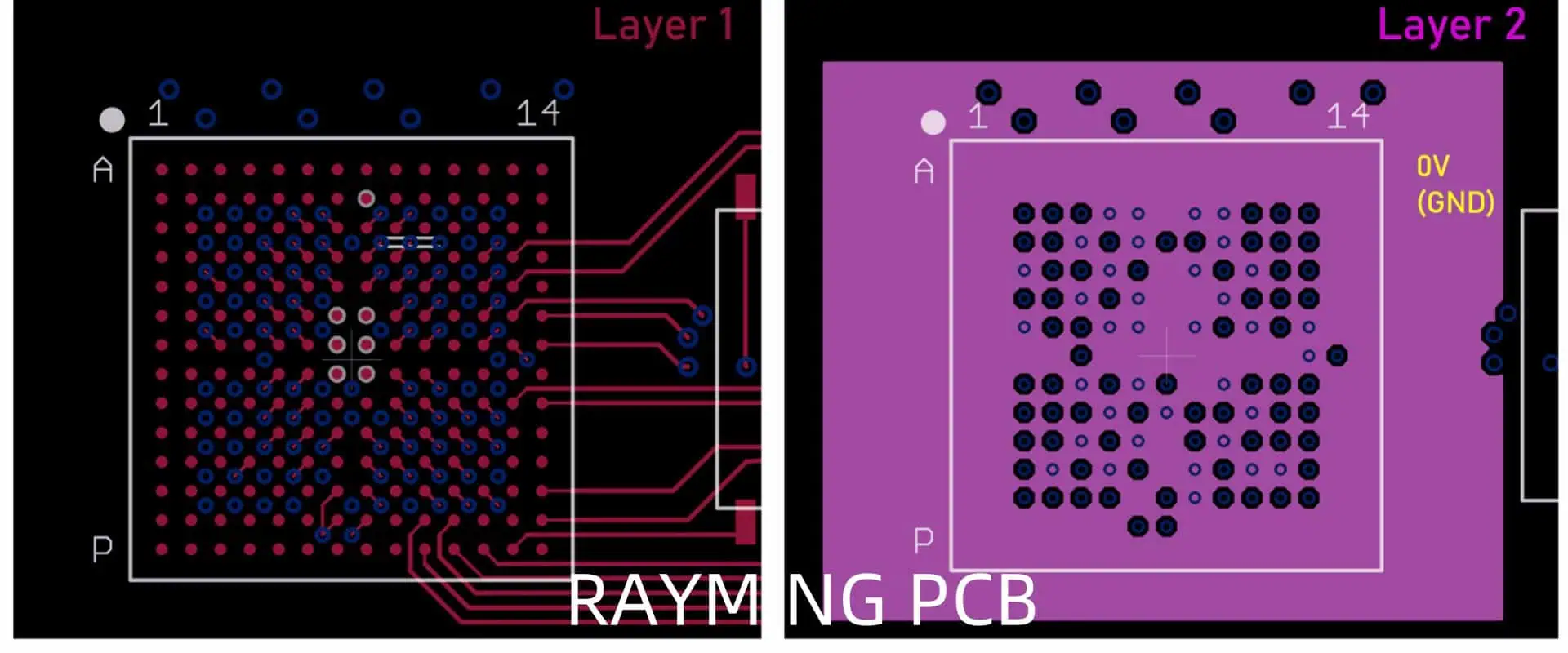
Minimizing Vias and Transitions
Vias and transitions between layers can introduce significant insertion loss, especially at high frequencies. To minimize their impact:
- Reduce the number of layer transitions for high-frequency signals.
- Use via stitching techniques to maintain consistent ground reference for microstrip lines.
- Implement backdrilling for high-speed signals to remove unused via stubs.
- Consider using blind and buried vias for critical signal paths.
Proper Grounding and Return Path Design
Effective grounding and return path design are crucial for minimizing insertion loss and maintaining signal integrity:
- Implement a solid ground plane directly adjacent to signal layers.
- Ensure uninterrupted return paths for all high-frequency signals.
- Use ground vias liberally to reduce ground inductance and improve return current flow.
- Consider using coplanar waveguide structures for improved ground reference.
Controlling Impedance and Minimizing Reflections
Maintaining consistent impedance throughout the signal path and minimizing reflections are critical for reducing insertion loss.
Impedance Control
RO4000 LoPro laminates offer excellent Dk and thickness tolerances, which facilitate precise impedance control. To leverage this:
- Work closely with your PCB fabricator to establish achievable impedance tolerances.
- Use field solvers to accurately calculate trace widths for target impedances.
- Implement proper stackup design to maintain consistent impedance across different layers.
- Consider using laser-direct imaging (LDI) for improved trace width control.
Minimizing Reflections
Reflections occur when there are impedance discontinuities in the signal path, contributing to insertion loss. To minimize reflections:
- Use smooth transitions between different transmission line structures.
- Implement proper termination techniques for high-frequency signals.
- Avoid abrupt changes in trace width or direction.
- Use chamfered bends for high-frequency traces to reduce reflections at corners.
Thermal Management Considerations
While RO4000 LoPro laminates offer excellent thermal stability, proper thermal management is still crucial for maintaining low insertion loss, especially in high-power applications.
Heat Dissipation Techniques
Effective heat dissipation helps maintain the stability of the dielectric properties and reduces the temperature-dependent component of insertion loss:
- Use thermal vias to improve heat transfer to ground planes.
- Consider using coin technology for areas with high power density.
- Implement proper component placement to optimize heat distribution.
- Use thermal simulation tools to identify and address potential hotspots.
Coefficient of Thermal Expansion (CTE) Matching
RO4000 LoPro laminates offer good CTE matching with copper, which helps maintain the integrity of plated through-holes and reduces stress on solder joints:
- Consider the CTE of other materials in your design (e.g., components, solder masks) for optimal thermal stability.
- Use proper layer sequencing in multilayer designs to balance thermal stresses.
- Implement proper curing and cooling processes during PCB fabrication.
Comparative Analysis: RO4000 LoPro vs. Standard Materials
To illustrate the benefits of RO4000 LoPro laminates, let’s compare their performance to standard FR-4 and other high-frequency materials in terms of key parameters affecting insertion loss.
| Material | Dk (@ 10 GHz) | Df (@ 10 GHz) | Copper Foil RMS Roughness (μm) | Thermal Conductivity (W/m/K) |
| RO4003C LoPro | 3.38 卤 0.05 | 0.0027 | < 0.4 | 0.71 |
| Standard FR-4 | 4.2 – 4.8 | 0.015 – 0.025 | 1.8 – 2.8 | 0.3 |
| PTFE-based Material | 2.2 – 2.5 | 0.0009 – 0.0020 | 0.5 – 1.0 | 0.25 |
| High-speed FR-4 | 3.9 – 4.2 | 0.008 – 0.012 | 1.5 – 2.0 | 0.4 |
As we can see from this comparison, RO4000 LoPro laminates offer a compelling combination of low Dk, low Df, and extremely smooth copper foil. These properties contribute significantly to reduced insertion loss compared to standard FR-4 and even some specialized high-frequency materials.
Case Studies: Successful Implementation of RO4000 LoPro Laminates
To further illustrate the practical benefits of using RO4000 LoPro laminates, let’s examine two case studies where these materials were successfully implemented to improve insertion loss in high-frequency applications.
Case Study 1: 5G Base Station Antenna Feed Network
A manufacturer of 5G base station equipment was facing challenges with signal integrity in their antenna feed networks operating at 28 GHz. They were experiencing higher than acceptable insertion loss, which was limiting the effective range and data throughput of their base stations.
Solution:
- Switched from standard high-frequency material to RO4350B LoPro laminate
- Redesigned the feed network to take advantage of the material’s low Dk and Df
- Implemented careful impedance control and minimized layer transitions
Results:
- Reduced insertion loss by 0.4 dB/inch at 28 GHz
- Improved overall antenna efficiency by 15%
- Increased base station coverage area by approximately 10%
Case Study 2: High-Speed Digital Backplane
A telecommunications equipment manufacturer was developing a new high-speed digital backplane for their next-generation routing platform. They needed to support data rates up to 56 Gbps NRZ (non-return-to-zero) while minimizing insertion loss to maintain signal integrity over long trace lengths.
Solution:
- Used RO4003C LoPro laminate for critical high-speed layers
- Implemented a hybrid stackup with RO4003C LoPro for high-speed layers and standard FR-4 for power and low-speed signal layers
- Utilized the low-profile copper to design ultra-smooth transmission lines
- Employed backdrilling to remove unused via stubs
Results:
- Achieved a 30% reduction in insertion loss compared to their previous design
- Successfully supported 56 Gbps NRZ signaling over 30-inch trace lengths
- Improved overall system throughput by 25% while maintaining backward compatibility with existing line cards
These case studies demonstrate the tangible benefits of using RO4000 LoPro laminates in real-world high-frequency applications, showcasing their ability to significantly improve insertion loss and overall system performance.
Future Trends and Developments
As the demand for higher frequency and higher data rate applications continues to grow, we can expect further developments in laminate technology and insertion loss reduction techniques. Some potential future trends include:
- Advanced copper foil treatments to further reduce surface roughness
- Development of ultra-low-loss dielectric materials
- Integration of advanced materials like graphene or carbon nanotubes into PCB laminates
- Improved simulation and modeling tools for more accurate prediction of insertion loss
- Novel PCB fabrication techniques to enhance signal integrity at mmWave frequencies
Staying informed about these developments and continually refining design practices will be crucial for engineers working on high-frequency applications.
Conclusion
Improving insertion loss is a critical consideration in high-frequency circuit design, and RO4000 LoPro laminates offer a powerful tool for achieving this goal. By leveraging the low dielectric constant, low dissipation factor, and smooth copper foil of these materials, designers can significantly enhance the performance of their high-frequency circuits.
Key strategies for maximizing the benefits of RO4000 LoPro laminates include:
- Optimizing dielectric properties through proper material selection and design
- Leveraging the low-profile copper foil to minimize conductor losses
- Implementing careful PCB design and layout techniques
- Controlling impedance and minimizing reflections throughout the signal path
- Considering thermal management to maintain stable performance
By combining these strategies with the advanced material properties of RO4000 LoPro laminates, engineers can push the boundaries of what’s possible in high-frequency circuit design, enabling the development of next-generation communication systems, radar technology, and other cutting-edge applications.
Frequently Asked Questions (FAQ)
- Q: What is the main advantage of using RO4000 LoPro laminates over standard FR-4 materials? A: The main advantage of RO4000 LoPro laminates is their significantly lower insertion loss at high frequencies. This is due to their lower dielectric constant, lower dissipation factor, and the use of low-profile copper foil, which all contribute to improved signal integrity and performance in high-frequency applications.
- Q: How do RO4000 LoPro laminates compare to PTFE-based materials in terms of insertion loss? A: While PTFE-based materials often have lower dissipation factors, RO4000 LoPro laminates offer a good balance of low insertion loss, ease of fabrication, and cost-effectiveness. They can achieve insertion loss performance close to that of PTFE materials in many applications, while being easier to process and more dimensionally stable.
- Q: Can RO4000 LoPro laminates be used in hybrid stackups with FR-4 materials? A: Yes, RO4000 LoPro laminates can be used in hybrid stackups with FR-4 materials. This approach is often used to balance performance and cost, with RO4000 LoPro layers used for critical high-frequency signals and FR-4 used for power, ground, and low-speed signals.
- Q: What is the maximum frequency at which RO4000 LoPro laminates can be effectively used? A: RO4000 LoPro laminates can be effectively used well into the mmWave frequency range. They have been successfully employed in applications operating at frequencies up to 77 GHz and beyond. However, the specific maximum usable frequency depends on the particular design requirements and acceptable loss thresholds.
- Q: Are there any special considerations for PCB fabrication when using RO4000 LoPro laminates? A: While RO4000 LoPro laminates are generally compatible with standard PCB fabrication processes, there are some considerations to keep in mind. These include using proper drilling and plating techniques to maintain the integrity of the low-profile copper