What is Lead-based (non-RoHS) Soldering?

Lead-based soldering has been a cornerstone of electronics manufacturing for decades. Despite recent regulations and shifts towards lead-free alternatives, lead-based soldering continues to play a crucial role in certain industries and applications. This article delves into the intricacies of lead-based soldering, its properties, applications, and the ongoing debate surrounding its use in the age of environmental consciousness.

The Basics of Lead-based Soldering

Definition and Composition

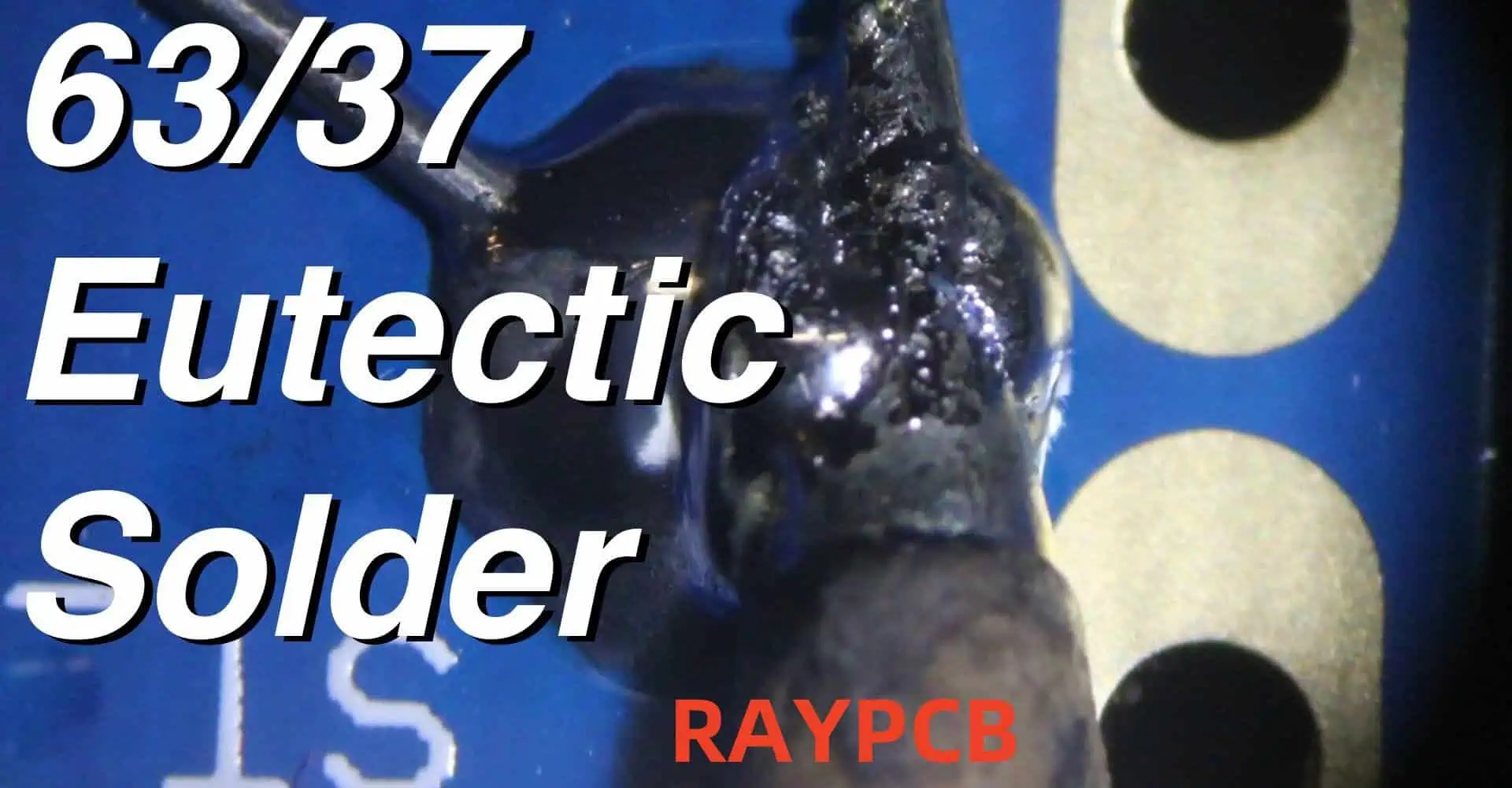
Lead-based solder is an alloy primarily composed of tin (Sn) and lead (Pb). The most common composition is 63% tin and 37% lead, known as 63/37 solder. This particular ratio is favored for its eutectic properties, meaning it has a single, low melting point.

Historical Context

Lead-based solders have been used for centuries in various applications, from plumbing to electronics. Their popularity in electronics stems from their excellent electrical conductivity, low melting point, and ease of use.

Properties of Lead-based Solder

Melting Point

One of the key advantages of lead-based solder is its relatively low melting point. The eutectic 63/37 solder melts at 183ยฐC (361ยฐF), which is significantly lower than many lead-free alternatives.

Electrical Conductivity

Lead-based solders offer excellent electrical conductivity, crucial for creating reliable connections in electronic circuits.

Mechanical Strength

While not as strong as some modern lead-free alternatives, lead-based solders provide adequate mechanical strength for many applications.

Wetting Properties

Lead-based solders have superior wetting properties, allowing them to flow easily and create strong bonds with various metals.

Comparison of Lead-based and Lead-free Solders

To better understand the differences between lead-based and lead-free solders, let’s compare their key properties:

PropertyLead-based Solder (63/37)Lead-free Solder (SAC305)
Melting Point183ยฐC (361ยฐF)217-220ยฐC (423-428ยฐF)
Electrical ConductivityExcellentGood
Mechanical StrengthGoodVery Good
Wetting PropertiesExcellentGood
CostLowerHigher
Environmental ImpactHigherLower

Applications of Lead-based Soldering

Military and Aerospace

The military and aerospace industries continue to rely on lead-based solders due to their proven reliability in harsh environments and long-term stability.

Medical Devices

Some medical devices still utilize lead-based solders, particularly in applications where long-term reliability is critical.

Automotive Electronics

While many automotive manufacturers have transitioned to lead-free solders, some specialized applications still use lead-based solders.

High-Reliability Electronics

Certain high-reliability electronics, such as those used in industrial control systems or telecommunications infrastructure, may still employ lead-based solders.

The RoHS Directive and Lead-based Soldering

Overview of RoHS

The Restriction of Hazardous Substances (RoHS) directive, implemented by the European Union in 2006, restricts the use of certain hazardous materials in electrical and electronic equipment.

Impact on Lead-based Soldering

RoHS has significantly reduced the use of lead-based solders in consumer electronics. However, it includes exemptions for certain applications where lead-free alternatives are not yet feasible or reliable.

Exemptions

Some exemptions to the RoHS directive include:

  1. High-melting temperature solders (>85% lead)
  2. Servers, storage, and storage array systems
  3. Network infrastructure equipment for switching, signaling, transmission, and network management

Advantages of Lead-based Soldering

Lower Melting Point

The lower melting point of lead-based solders reduces thermal stress on components during the soldering process.

Cost-effectiveness

Lead-based solders are generally less expensive than their lead-free counterparts.

Proven Reliability

Decades of use have demonstrated the long-term reliability of lead-based solders in various applications.

Ease of Use

Lead-based solders are known for their excellent wetting properties and ease of application, making them user-friendly for both automated and manual soldering processes.

Disadvantages and Environmental Concerns

Health Risks

Lead is a known neurotoxin, posing health risks to workers and potentially to end-users if not properly managed.

Environmental Impact

Improper disposal of lead-containing electronics can lead to environmental contamination.

Regulatory Restrictions

Increasing regulations worldwide are limiting the use of lead-based solders, requiring manufacturers to adapt their processes.

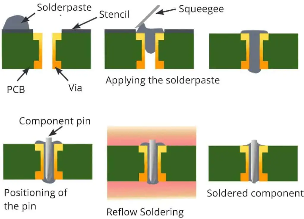
Techniques and Best Practices for Lead-based Soldering

Desoldering Wick vs. Pump

Temperature Control

Proper temperature control is crucial for achieving high-quality solder joints. The optimal soldering temperature for 63/37 solder is typically between 315-370ยฐC (600-700ยฐF).

Flux Selection

Choosing the right flux is essential for removing oxides and promoting good wetting. Rosin-based fluxes are commonly used with lead-based solders.

Proper Ventilation

Adequate ventilation is crucial to minimize exposure to lead fumes during the soldering process.

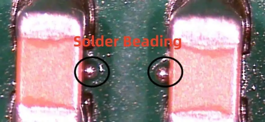
Cleaning and Inspection

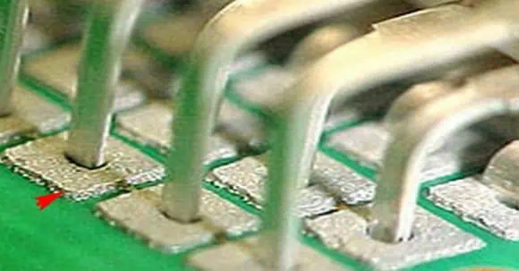
Thorough cleaning and inspection of solder joints are necessary to ensure reliability and remove any flux residues.

Lead-based Soldering Equipment
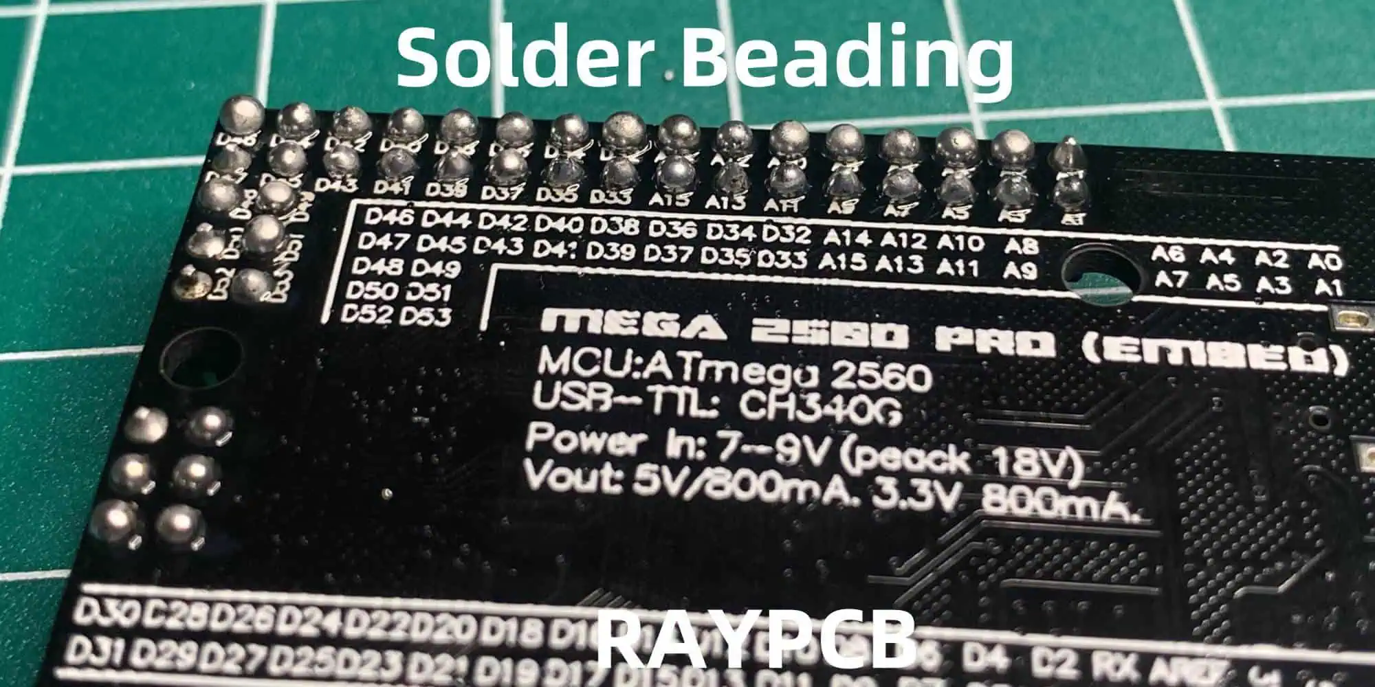
Soldering Irons

Temperature-controlled soldering irons are essential for precise and consistent results.

Solder Baths

Solder baths or pots are used for dip soldering applications, particularly in through-hole assembly.

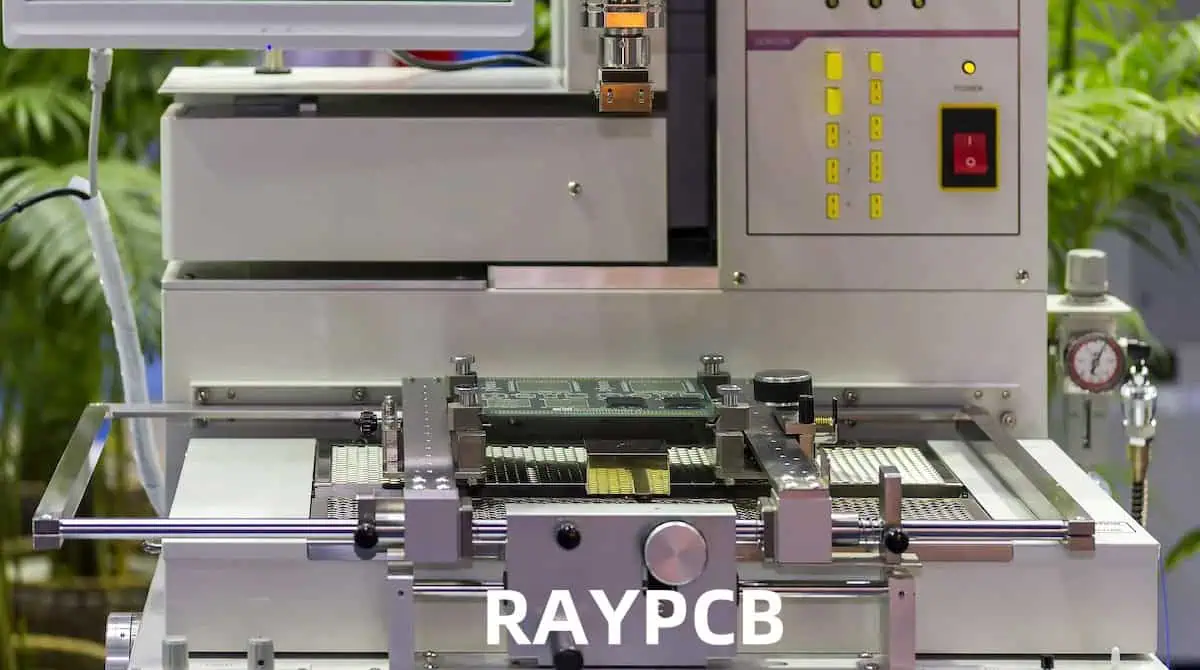
Wave Soldering Machines

Wave soldering machines are used for high-volume production, particularly for through-hole components.

Future of Lead-based Soldering

Ongoing Research

Research continues into lead-free alternatives that can match or exceed the performance of lead-based solders.

Regulatory Trends

Global regulations are likely to further restrict the use of lead-based solders, even in currently exempt applications.

Industry Adaptation

Industries still relying on lead-based solders are actively seeking alternatives and adapting their processes to comply with evolving regulations.

Conclusion

Lead-based soldering, while facing increasing regulatory pressure, continues to play a vital role in specific industries and applications. Its unique properties, proven reliability, and cost-effectiveness make it difficult to replace entirely. However, the ongoing shift towards lead-free alternatives is driven by valid environmental and health concerns. As technology advances, it’s likely that lead-based soldering will become increasingly niche, reserved only for the most demanding applications where no suitable alternatives exist.

FAQ

  1. Q: Is lead-based soldering illegal? A: Lead-based soldering is not illegal globally, but its use is restricted in many countries, particularly for consumer electronics. Certain industries and applications are exempt from these restrictions.
  2. Q: What are the main differences between lead-based and lead-free solders? A: The main differences include melting point (lead-based is lower), cost (lead-based is generally cheaper), environmental impact (lead-free is better), and ease of use (lead-based is typically easier to work with).
  3. Q: Can I use lead-based solder for hobby electronics projects? A: While it’s still possible to obtain lead-based solder for hobby use, many hobbyists are transitioning to lead-free alternatives due to health and environmental concerns. Always check local regulations and handle lead-based solder with proper safety precautions.
  4. Q: Why do some industries still use lead-based solder despite the known risks? A: Some industries, particularly those requiring high reliability in extreme conditions (like aerospace or military applications), continue to use lead-based solder due to its proven long-term reliability and performance characteristics that are challenging to match with current lead-free alternatives.
  5. Q: How can I safely dispose of electronics containing lead-based solder? A: Electronics containing lead-based solder should be disposed of as electronic waste (e-waste) through proper recycling channels. Many communities have dedicated e-waste collection points or events. Never dispose of these items in regular trash to prevent environmental contamination.

What is IPC-2581?

PCB IPC standards

In the ever-evolving world of electronics manufacturing, efficient and accurate data exchange between design and production stages is crucial. IPC-2581, also known as the “Generic Requirements for Printed Board Assembly Products Manufacturing Description Data and Transfer Methodology,” is a standard that addresses this need. This comprehensive article will explore the intricacies of IPC-2581, its significance in the electronics industry, and its impact on the PCB design and manufacturing process.

Understanding IPC-2581

Definition and Purpose

IPC-2581 is an open, neutral, and extensible data format standard developed by the IPC (Institute of Printed Circuits) to streamline the exchange of printed circuit board (PCB) design, fabrication, and assembly data. Its primary purpose is to provide a single, comprehensive XML-based data format that can replace multiple files typically used in the PCB manufacturing process.

Historical Context

Evolution of PCB Data Exchange Standards

  1. Gerber Format (RS-274D, RS-274X)
  2. ODB++ (Open Database++)
  3. IPC-2511 (GenCAM)
  4. IPC-2581 (Current standard)

Key Features of IPC-2581

  1. XML-based format
  2. Single file containing all necessary data
  3. Support for complex board structures
  4. Embedded component information
  5. Stackup details
  6. Manufacturing process instructions

The Structure of IPC-2581

Data Hierarchy

  1. Header Information
  2. Board Outline
  3. Stackup Definition
  4. Component Definitions
  5. Placement Data
  6. Artwork Data
  7. Test Points
  8. Manufacturing Instructions

XML Schema

The IPC-2581 standard uses an XML schema to define the structure and content of the data file. This schema ensures consistency and validation of the data across different software platforms.

Advantages of IPC-2581

IPC-for-pcb

Comprehensive Data Exchange

IPC-2581 eliminates the need for multiple file formats by consolidating all necessary information into a single file.

Improved Accuracy

By reducing the number of files and translations required, IPC-2581 minimizes the risk of data loss or corruption.

Enhanced Efficiency

The use of a single file format streamlines the design-to-manufacturing process, reducing time and potential errors.

Vendor Neutrality

As an open standard, IPC-2581 is not tied to any specific software vendor, promoting interoperability across different tools and systems.

Future-Proofing

The extensible nature of XML allows for easy updates and additions to the standard as technology evolves.

Challenges in IPC-2581 Adoption

Legacy System Compatibility

Many existing systems are built around older file formats, requiring significant updates to support IPC-2581.

Industry Inertia

The PCB industry has been slow to change, with many companies hesitant to move away from established processes.

Software Support

While growing, the number of software tools fully supporting IPC-2581 is still limited compared to older formats.

Training and Education

Adopting IPC-2581 requires training for design and manufacturing personnel to effectively use the new format.

IPC-2581 in the PCB Design Process

Design Creation

  1. Schematic Capture
  2. Component Selection
  3. PCB Layout
  4. Design Rule Checking

Data Export

  1. Generating IPC-2581 File
  2. Validation of Exported Data
  3. Review and Approval Process

Design Handoff

  1. Transferring IPC-2581 File to Manufacturers
  2. Addressing Manufacturer Queries
  3. Design Revisions and Version Control

IPC-2581 in PCB Manufacturing

Data Import and Validation

  1. Loading IPC-2581 File into CAM Systems
  2. Automated Design Rule Checking
  3. Identifying and Resolving Data Discrepancies

Fabrication Process

  1. Generating Manufacturing Tooling
  2. Stackup Creation
  3. Drill and Rout Programming

Assembly Process

  1. Component Placement Programming
  2. Solder Paste Stencil Design
  3. Automated Optical Inspection (AOI) Programming

Comparison of PCB Data Exchange Formats

To better understand the position of IPC-2581 in the context of PCB data exchange, let’s compare it with other common formats:

FeatureIPC-2581GerberODB++GenCAM
File FormatXMLASCIIProprietarySGML
Number of FilesSingleMultipleMultipleSingle
Stackup InformationYesLimitedYesYes
Component DataYesNoYesYes
Manufacturing InstructionsYesNoYesYes
Netlist InformationYesNoYesYes
ExtensibilityHighLowMediumMedium
Industry AdoptionGrowingHighHighLow
Vendor NeutralityHighHighLowHigh

IPC-2581 Consortium

Purpose and Goals

The IPC-2581 Consortium is an industry group dedicated to promoting and accelerating the adoption of the IPC-2581 standard.

Key Activities

  1. Standard Development and Maintenance
  2. Industry Outreach and Education
  3. Interoperability Testing and Validation
  4. Collaboration with Software Vendors

Member Companies

The consortium includes a diverse range of companies from the electronics industry, including:

  1. PCB Design Software Providers
  2. Electronic Design Automation (EDA) Companies
  3. PCB Manufacturers
  4. Electronics Assembly Companies
  5. Original Equipment Manufacturers (OEMs)

Future Trends in IPC-2581

Integration with Industry 4.0

Exploring ways to incorporate IPC-2581 into smart manufacturing and IoT systems.

Enhanced Security Features

Developing methods for secure data transfer and intellectual property protection within the IPC-2581 format.

Artificial Intelligence and Machine Learning

Leveraging AI and ML techniques for improved data validation and manufacturing process optimization.

Cloud-Based Collaboration

Facilitating cloud-based design and manufacturing collaboration using IPC-2581 as the central data format.

Expansion to New Technologies

Adapting IPC-2581 to support emerging technologies such as flexible electronics and 3D-printed electronics.

Best Practices for IPC-2581 Implementation

Comprehensive Training

Provide thorough training for design and manufacturing teams on IPC-2581 usage and benefits.

Phased Adoption

Implement IPC-2581 in stages, starting with pilot projects before full-scale adoption.

Software Evaluation

Carefully assess and select software tools that fully support IPC-2581 functionality.

Collaboration with Partners

Work closely with manufacturing partners to ensure smooth data exchange and process integration.

Continuous Improvement

Regularly review and update IPC-2581 implementation processes based on feedback and industry developments.

Economic Impact of IPC-2581 Adoption

To illustrate the potential economic benefits of implementing IPC-2581 in a PCB design and manufacturing environment, consider the following hypothetical scenario:

FactorWithout IPC-2581With IPC-2581
Annual PCB Designs100100
Average Design-to-Manufacturing Time5 days3 days
Design Revisions Due to Data Issues20%5%
Cost per Day of Delay$5,000 $5,000 
Annual Delay Costs$100,000 $15,000 
Data Translation Software Costs$50,000 $10,000 
Training and Implementation Costs$0 $25,000 
Total Annual Costs$150,000 $50,000 
Annual Savings$100,000 

This simplified example demonstrates how the adoption of IPC-2581 can lead to significant cost savings through reduced design-to-manufacturing time, fewer revisions, and streamlined software requirements, despite initial training and implementation costs.

Frequently Asked Questions (FAQ)

1. How does IPC-2581 differ from Gerber files?

IPC-2581 differs from Gerber files in several key aspects:

a) File Format: IPC-2581 uses a single XML-based file, while Gerber requires multiple files for different layers and data types.

b) Comprehensiveness: IPC-2581 includes all necessary PCB data (layout, stackup, components, etc.) in one file, whereas Gerber primarily focuses on image data for each layer.

c) Intelligent Data: IPC-2581 contains intelligent data about components, nets, and manufacturing instructions, which Gerber files lack.

d) Stackup Information: IPC-2581 includes detailed stackup data, while Gerber files typically require separate documentation for this information.

e) Extensibility: As an XML-based format, IPC-2581 is easily extensible to accommodate new technologies, while Gerber has limited extensibility.

f) Manufacturing Instructions: IPC-2581 can include specific manufacturing and assembly instructions, which are not part of the Gerber format.

g) Netlist Information: IPC-2581 includes netlist data, which is not present in Gerber files.

The comprehensive nature of IPC-2581 allows for a more streamlined and accurate design-to-manufacturing process compared to the traditional Gerber approach.

2. What are the main challenges in adopting IPC-2581?

The main challenges in adopting IPC-2581 include:

a) Software Support: Not all PCB design and manufacturing software fully support IPC-2581, limiting its widespread adoption.

b) Industry Inertia: Many companies are resistant to change, preferring to stick with familiar formats like Gerber.

c) Training Requirements: Adopting IPC-2581 requires training for design and manufacturing personnel, which can be time-consuming and costly.

d) Legacy System Compatibility: Existing manufacturing systems may require significant updates to support IPC-2581.

e) Supply Chain Alignment: All parties in the supply chain (designers, fabricators, assemblers) need to support IPC-2581 for maximum benefit.

f) Initial Implementation Costs: There may be upfront costs associated with software upgrades and process changes.

g) Data Validation: Ensuring the accuracy and completeness of IPC-2581 files requires new validation processes.

h) Intellectual Property Concerns: Some companies may be hesitant to include all design data in a single file due to IP protection concerns.

Overcoming these challenges often requires a coordinated effort between design teams, manufacturers, and software vendors, as well as a clear understanding of the long-term benefits of IPC-2581 adoption.

3. Can IPC-2581 completely replace all other PCB data formats?

While IPC-2581 has the potential to replace many existing PCB data formats, it may not completely replace all formats in the short term due to several factors:

a) Legacy Systems: Many manufacturers still rely on older formats and may be slow to upgrade their systems.

b) Specialized Formats: Some niche applications may require specialized formats not fully covered by IPC-2581.

c) Industry Adoption Rate: Widespread adoption takes time, and some sectors may be slower to transition.

d) Regulatory Requirements: Certain industries or regions may have specific requirements that necessitate the use of particular formats.

e) Vendor-Specific Features: Some proprietary formats may offer unique features that companies are reluctant to abandon.

f) Parallel Use: During the transition period, companies may use IPC-2581 alongside other formats to ensure compatibility.

g) Design Tool Limitations: Not all PCB design tools fully support IPC-2581 export, necessitating the use of other formats.

h) Verification and Comparison: Some companies may continue to use multiple formats for cross-verification purposes.

While IPC-2581 offers significant advantages and could potentially become the primary PCB data exchange format, it’s likely that other formats will continue to coexist in the industry for some time. The goal is for IPC-2581 to become the central, comprehensive format while potentially interfacing with other specialized or legacy formats as needed.

4. How does IPC-2581 handle revisions and version control?

IPC-2581 incorporates several features to handle revisions and version control effectively:

a) Revision Attributes: The standard includes specific attributes for revision numbers and dates, allowing clear tracking of design versions.

b) Change History: IPC-2581 can include a change history section, detailing modifications made between versions.

c) Component Revisions: Individual component revisions can be specified within the file, allowing for granular tracking of part changes.

d) Layer Versioning: Each layer in the PCB stackup can have its own revision information.

e) Global Unique Identifiers (GUIDs): Use of GUIDs for various elements allows for consistent tracking across revisions.

f) Annotation and Comments: The format supports detailed annotations and comments, which can be used to document changes.

g) ECO (Engineering Change Order) Support: IPC-2581 can include ECO information, linking design changes to specific orders.

h) Differential Comparisons: The XML structure facilitates easy comparison between different versions of a design.

i) Metadata: Additional metadata fields can be used to store version control information from external systems.

These features allow for comprehensive version control within the IPC-2581 file itself, facilitating clear communication of design changes throughout the supply chain. However, it’s important to note that effective version control also relies on proper processes and practices in addition to the capabilities of the file format.

5. What steps should a company take to implement IPC-2581 in their workflow?

Implementing IPC-2581 in a company’s workflow involves several key steps:

a) Assessment:

  • Evaluate current workflows and identify areas where IPC-2581 can provide benefits
  • Assess the capability of existing software tools to support IPC-2581

b) Planning:

  • Develop a phased implementation plan
  • Set clear goals and metrics for the implementation

c) Software Updates:

  • Upgrade or acquire PCB design software that supports IPC-2581 export
  • Ensure CAM and manufacturing systems can import and process IPC-2581 files

d) Training:

  • Provide comprehensive training for design and manufacturing teams
  • Develop internal guidelines and best practices for working with IPC-2581

e) Pilot Project:

  • Start with a small-scale pilot project to test the implementation
  • Gather feedback and identify any issues or bottlenecks

f) Supply Chain Collaboration:

  • Communicate with manufacturing partners about the transition to IPC-2581
  • Ensure all parties in the supply chain are prepared to work with the new format

g) Process Refinement:

  • Based on the pilot project results, refine internal processes and workflows
  • Develop new quality control and validation procedures for IPC-2581 files

h) Full Implementation:

  • Gradually expand the use of IPC-2581 across more projects
  • Monitor and measure the impact on efficiency and quality

i) Continuous Improvement:

  • Regularly review and update IPC-2581 implementation processes
  • Stay informed about updates to the IPC-2581 standard and industry best practices

j) Feedback and Participation:

  • Provide feedback to software vendors and the IPC-2581 Consortium
  • Consider participating in industry groups to share experiences and contribute to the standard’s development

By following these steps, companies can systematically implement IPC-2581 and maximize the benefits of this comprehensive data exchange format. It’s important to approach the implementation as a strategic initiative, involving all relevant stakeholders and allowing time for adaptation and optimization.

What is High Potential (HiPot) Testing?

In the realm of electrical safety and quality assurance, High Potential (HiPot) testing stands as a critical procedure. This essential test, also known as Dielectric Withstand Testing or Voltage Breakdown Testing, plays a crucial role in ensuring the safety and reliability of electrical and electronic products. From consumer electronics to industrial machinery, HiPot testing is a fundamental step in verifying the integrity of electrical insulation and the overall safety of devices that rely on electrical power.

Understanding High Potential (HiPot) Testing

Definition and Purpose

High Potential testing is a non-destructive test method used to verify the electrical insulation of a device or component. The primary purpose of HiPot testing is to ensure that the insulation can withstand high voltage levels without breakdown, thereby preventing electrical hazards such as short circuits, arcing, or electrical shocks.

Basic Principles

HiPot testing operates on a simple yet effective principle: applying a high voltage between the conducting parts of a device and its external conductive surfaces or ground. This test voltage is significantly higher than the normal operating voltage of the device, typically ranging from 1000V to several thousand volts, depending on the application and safety standards.

Types of HiPot Tests

  1. AC HiPot Test
  2. DC HiPot Test
  3. Impulse (Surge) HiPot Test

The HiPot Testing Process

Equipment Setup

  1. HiPot Tester: The main testing device
  2. Test Fixtures: Custom-designed for specific products
  3. Safety Interlocks: To prevent accidental exposure to high voltages
  4. Monitoring Devices: For measuring leakage current and breakdown events

Test Procedure

  1. Device Under Test (DUT) Connection
  2. Safety Check and Parameter Setting
  3. Voltage Ramp-Up
  4. Hold Time at Test Voltage
  5. Monitoring and Measurement
  6. Voltage Ramp-Down
  7. Result Analysis and Recording

Safety Considerations

  1. Operator Training
  2. Proper Grounding
  3. Use of Personal Protective Equipment (PPE)
  4. Test Area Isolation
  5. Emergency Shutdown Procedures

Applications of HiPot Testing

Industries Utilizing HiPot Testing

  1. Consumer Electronics
  2. Medical Devices
  3. Automotive
  4. Aerospace
  5. Industrial Equipment
  6. Power Distribution

Specific Use Cases

  1. Household Appliance Safety Verification
  2. Electric Vehicle Battery Insulation Testing
  3. Aircraft Wiring Harness Validation
  4. Medical Imaging Equipment Certification
  5. Power Transformer Insulation Checking
  6. Industrial Motor Winding Inspection

Advantages of HiPot Testing

Early Defect Detection

HiPot testing can identify insulation weaknesses before they lead to product failure or safety hazards.

Quality Assurance

It provides a reliable method for verifying the manufacturing quality of electrical products.

Regulatory Compliance

Many safety standards and regulations require HiPot testing as part of product certification.

Cost-Effective

Detecting insulation issues early in the production process can prevent costly recalls and liability issues.

Versatility

HiPot testing can be applied to a wide range of electrical and electronic products.

Limitations and Challenges of HiPot Testing

Potential for Product Damage

Improper testing parameters can stress or damage the insulation of the device under test.

False Positives and Negatives

Incorrect test setup or interpretation can lead to erroneous results.

Time Consumption

HiPot testing can be time-consuming, especially for complex products or high-volume production.

Specialized Equipment and Expertise

Proper HiPot testing requires specific equipment and trained personnel.

Limited Information

While HiPot testing can detect insulation weaknesses, it may not provide detailed information about the nature or location of the defect.

Best Practices for HiPot Testing

Test Parameter Selection

Carefully choose voltage levels, ramp rates, and hold times based on product specifications and relevant standards.

Regular Equipment Calibration

Ensure HiPot testers are regularly calibrated to maintain accuracy.

Comprehensive Test Plans

Develop detailed test plans that cover all critical insulation points of the product.

Environmental Control

Conduct tests in controlled environments to minimize the impact of temperature and humidity on results.

Data Recording and Traceability

Maintain detailed records of test results for quality control and regulatory compliance.

Comparison of HiPot Testing Methods

To better understand the different approaches to HiPot testing, let’s compare the three main types:

CharacteristicAC HiPot TestDC HiPot TestImpulse HiPot Test
Voltage TypeAlternating CurrentDirect CurrentHigh-Voltage Pulse
Test DurationShort (seconds)Longer (minutes)Very Short (microseconds)
Stress on InsulationHighLower than ACVery High
Leakage Current MeasurementEasyMore ComplexChallenging
Typical ApplicationsProduction TestingField Testing, CablesSurge Protection Devices
Sensitivity to Capacitive EffectsHighLowModerate
Equipment CostModerateLowerHigher
Suitability for Capacitive LoadsLimitedGoodExcellent

HiPot Testing Standards and Regulations

International Standards

  1. IEC 60950: Information Technology Equipment
  2. IEC 61010: Measurement, Control, and Laboratory Equipment
  3. IEC 60601: Medical Electrical Equipment

Regional Standards

  1. UL 1012 (North America): Power Units Other Than Class 2
  2. EN 50191 (Europe): Erection and Operation of Electrical Test Equipment
  3. AS/NZS 3760 (Australia/New Zealand): In-service Safety Inspection and Testing of Electrical Equipment

Industry-Specific Standards

  1. DO-160 (Aerospace): Environmental Conditions and Test Procedures for Airborne Equipment
  2. ISO 6469-3 (Automotive): Electrically Propelled Road Vehicles – Safety Specifications
  3. IEC 62477-1 (Power Electronics): Safety Requirements for Power Electronic Converter Systems and Equipment

Future Trends in HiPot Testing

Integration with IoT and Industry 4.0

Incorporating HiPot testers into connected factory systems for real-time monitoring and data analysis.

Advanced Data Analytics

Utilizing machine learning algorithms to improve defect detection and predict potential insulation failures.

Automation and Robotics

Developing automated HiPot testing systems to increase efficiency and reduce human error.

Non-Contact Testing Methods

Exploring new technologies for performing HiPot tests without direct electrical contact.

Eco-Friendly Testing Solutions

Developing more energy-efficient and environmentally friendly HiPot testing equipment.

Economic Impact of HiPot Testing

To illustrate the potential economic benefits of implementing HiPot testing in a manufacturing environment, consider the following hypothetical scenario:

FactorWithout HiPot TestingWith HiPot Testing
Annual Production Volume1,000,000 units1,000,000 units
Defect Rate0.50%0.10%
Cost per Defective Unit$100 $100 
Annual Defect Cost$500,000 $100,000 
HiPot Testing Equipment Cost$0 $50,000 
Annual Testing Cost$0 $100,000 
Total Annual Cost$500,000 $250,000 
Annual Savings$250,000 

This simplified example demonstrates how the implementation of HiPot testing can lead to significant cost savings through reduced defect rates and associated expenses, despite the initial investment in equipment and ongoing testing costs.

Frequently Asked Questions (FAQ)

1. What is the difference between AC and DC HiPot testing?

AC and DC HiPot testing differ in several key aspects:

a) Voltage Type: AC HiPot uses alternating current, while DC HiPot uses direct current.

b) Test Duration: AC tests are typically shorter (seconds) compared to DC tests (minutes).

c) Stress on Insulation: AC testing generally stresses the insulation more than DC testing.

d) Leakage Current Measurement: AC leakage current is easier to measure accurately compared to DC.

e) Applications: AC testing is more common in production environments, while DC testing is often used for field testing and testing of cables or capacitive loads.

f) Sensitivity to Capacitive Effects: AC testing is more sensitive to capacitive effects in the device under test.

g) Equipment Complexity: DC HiPot testers are generally simpler and less expensive than AC testers.

The choice between AC and DC HiPot testing often depends on the specific application, product characteristics, and relevant safety standards.

2. How is the HiPot test voltage determined for a given product?

The HiPot test voltage is typically determined based on several factors:

a) Safety Standards: Many industry-specific standards specify the required test voltage based on the product’s normal operating voltage.

b) Operating Voltage: The test voltage is usually set at a multiple of the product’s maximum operating voltage. Common multipliers range from 1.5 to 2.5 times the operating voltage.

c) Insulation Type: Different insulation materials have varying breakdown voltages, which influence the test voltage selection.

d) Product Design: The physical construction and spacing between conductive parts can affect the appropriate test voltage.

e) Environmental Factors: Products intended for use in harsh environments may require higher test voltages.

f) Historical Data: Previous testing experience with similar products can inform voltage selection.

g) Margin of Safety: A balance must be struck between ensuring safety and avoiding damage to the product.

h) Regulatory Requirements: Some regions or industries may have specific requirements for HiPot test voltages.

It’s crucial to consult relevant safety standards and product specifications when determining the appropriate HiPot test voltage. Over-testing can damage the product, while under-testing may fail to identify potential safety hazards.

3. Can HiPot testing damage the device under test?

While HiPot testing is designed to be non-destructive, there is a potential for damage to the device under test (DUT) if not performed correctly:

a) Overvoltage: Applying a voltage significantly higher than the specified test voltage can break down the insulation.

b) Extended Test Duration: Prolonged exposure to high voltage can stress and degrade insulation materials.

c) Repeated Testing: Excessive retesting of the same unit can cumulatively stress the insulation.

d) Moisture Presence: Testing in high humidity conditions can lead to partial discharges and insulation degradation.

e) Improper Connections: Poor contact or incorrect wiring during testing can cause arcing or localized damage.

f) Voltage Transients: Rapid voltage changes, especially during ramp-up or ramp-down, can stress sensitive components.

g) Component Sensitivity: Some electronic components, particularly in modern, low-voltage circuits, can be sensitive to high voltages.

h) Insulation Aging: Older products or those exposed to harsh environments may have weakened insulation more susceptible to damage.

To minimize the risk of damage:

  1. Follow manufacturer guidelines and relevant standards for test parameters.
  2. Ensure proper training for test operators.
  3. Regularly calibrate and maintain test equipment.
  4. Implement appropriate safety measures and interlocks.
  5. Consider the specific characteristics and sensitivities of the DUT when designing the test protocol.

4. How often should HiPot testing be performed in a production environment?

The frequency of HiPot testing in a production environment depends on several factors:

a) Regulatory Requirements: Some industries mandate 100% testing of all units produced.

b) Product Complexity: More complex products may require more frequent testing.

c) Safety Criticality: Products with high safety requirements often need more frequent or even 100% testing.

d) Production Volume: High-volume production might use statistical process control to determine testing frequency.

e) Historical Quality Data: Products with a history of insulation issues may require more frequent testing.

f) Manufacturing Process Stability: More stable processes might allow for reduced testing frequency.

g) Cost Considerations: Balancing testing costs with potential risks and liabilities.

h) Customer Requirements: Some customers or markets may specify testing frequency.

Common approaches include:

  1. 100% Testing: Every unit is tested before shipping.
  2. Batch Testing: A sample from each production batch is tested.
  3. Periodic Testing: Testing is performed at regular intervals (e.g., hourly, daily).
  4. Start/End of Run Testing: Testing the first and last units of a production run.
  5. Statistical Sampling: Testing based on statistical quality control methods.

It’s important to develop a testing strategy that ensures product safety and quality while considering production efficiency and costs. Regular review and adjustment of the testing frequency based on quality data and process changes is recommended.

5. What are the key safety precautions for performing HiPot tests?

Ensuring safety during HiPot testing is crucial due to the high voltages involved. Key safety precautions include:

a) Operator Training: Ensure all personnel are properly trained in HiPot testing procedures and safety protocols.

b) Personal Protective Equipment (PPE): Use appropriate PPE such as insulating gloves and safety glasses.

c) Test Area Isolation: Designate and clearly mark the HiPot testing area, restricting access to authorized personnel only.

d) Safety Interlocks: Implement fail-safe interlocks that cut power if safety barriers are breached.

e) Proper Grounding: Ensure all equipment and the operator are properly grounded to prevent electric shock.

f) Emergency Shutdown: Install easily accessible emergency stop buttons near the test area.

g) Warning Signs: Display clear warning signs indicating high voltage hazards in the test area.

h) Equipment Inspection: Regularly inspect and maintain HiPot testers and associated equipment.

i) No Lone Working: Implement a buddy system or supervision for HiPot testing operations.

j) Discharge Procedures: Follow proper procedures for discharging devices after testing, especially for DC HiPot tests.

k) Ventilation: Ensure adequate ventilation to dissipate ozone produced during AC HiPot testing.

l) Flammable Materials: Keep flammable materials away from the test area to prevent fire hazards.

m) Test Fixture Design: Use properly insulated and guarded test fixtures to prevent accidental contact with high voltage.

n) Regular Safety Audits: Conduct periodic safety audits of the HiPot testing process and equipment.

o) Documentation: Maintain clear, up-to-date safety procedures and ensure they are readily accessible to all operators.

By adhering to these safety precautions, organizations can minimize the risks associated with HiPot testing and create a safer working environment for their employees.

What is Eutectic Solder?

In the world of electronics manufacturing and metallurgy, the term “eutectic solder” is frequently encountered. This crucial material plays a vital role in creating reliable electrical and mechanical connections in a wide range of applications. To fully appreciate its importance and unique properties, we need to delve deep into the science behind eutectic solder, its composition, characteristics, and applications.

Understanding Eutectic Alloys

Definition of Eutectic

The term “eutectic” comes from the Greek word “eutฤ“ktos,” meaning “easily melted.” In metallurgy, a eutectic composition refers to a mixture of two or more components that melts and solidifies at a single temperature, which is lower than the melting points of the individual components.

The Eutectic Point

The eutectic point is a specific composition and temperature at which a eutectic mixture exhibits its unique properties. At this point, the liquid and solid phases of the alloy are in equilibrium.

Phase Diagram Basics

To understand eutectic alloys, it’s essential to be familiar with phase diagrams. These graphical representations show the relationships between temperature, composition, and the phases present in an alloy system.

Eutectic Solder Composition

Common Eutectic Solder Alloys

Several eutectic solder compositions are used in various industries. Here are some of the most common:

Alloy CompositionEutectic Temperature (ยฐC)Primary Applications
63% Sn / 37% Pb183Electronics (legacy)
96.5% Sn / 3.5% Ag221Lead-free electronics
91% Sn / 9% Zn199Aluminum soldering
52% In / 48% Sn118Low-temperature applications
80% Au / 20% Sn280High-reliability electronics

Lead-Based vs. Lead-Free Eutectic Solders

Lead-Based Eutectic Solder

Traditionally, the most widely used eutectic solder was the tin-lead (Sn-Pb) alloy with a composition of 63% tin and 37% lead. This alloy has a eutectic temperature of 183ยฐC (361ยฐF).

Lead-Free Eutectic Solder

Due to environmental and health concerns, lead-free alternatives have been developed. The most common lead-free eutectic solder is the tin-silver (Sn-Ag) alloy, typically composed of 96.5% tin and 3.5% silver, with a eutectic temperature of 221ยฐC (430ยฐF).

Properties of Eutectic Solder

Melting Behavior

The defining characteristic of eutectic solder is its sharp melting point. Unlike non-eutectic alloys that melt over a range of temperatures, eutectic solders transition directly from solid to liquid at a specific temperature.

Mechanical Properties

Eutectic solders generally exhibit:

  1. Good tensile strength
  2. Excellent ductility
  3. Resistance to fatigue

Electrical Properties

Eutectic solders are chosen for their:

  1. Low electrical resistance
  2. Good conductivity
  3. Stability under various operating conditions

Wetting Characteristics

Eutectic solders typically display excellent wetting properties, which is crucial for forming strong and reliable solder joints.

Applications of Eutectic Solder

Electronics Manufacturing

  1. Printed Circuit Board (PCB) Assembly
  2. Component Attachment
  3. Ball Grid Array (BGA) Soldering

Automotive Industry

  1. Engine Control Units
  2. Sensor Connections
  3. Power Electronics

Aerospace and Defense

  1. Satellite Components
  2. Avionics Systems
  3. Military Communication Equipment

Medical Devices

  1. Implantable Devices
  2. Diagnostic Equipment
  3. Surgical Instruments

Renewable Energy

  1. Solar Panel Connections
  2. Wind Turbine Control Systems
  3. Battery Management Systems

Advantages of Using Eutectic Solder

Precise Melting Point

The sharp melting point of eutectic solder allows for more precise control during the soldering process, reducing the risk of component damage due to excessive heat exposure.

Improved Joint Reliability

Eutectic solders tend to form stronger, more reliable joints due to their consistent microstructure and lack of a “mushy” zone during solidification.

Enhanced Production Efficiency

The predictable behavior of eutectic solders can lead to faster production times and reduced defect rates in manufacturing processes.

Better Thermal Cycling Performance

Eutectic solder joints often exhibit better resistance to thermal fatigue, which is crucial in applications subject to temperature fluctuations.

Challenges and Considerations

Higher Melting Points of Lead-Free Alternatives

Many lead-free eutectic solders have higher melting points compared to traditional tin-lead solders, requiring adjustments to manufacturing processes and potentially affecting heat-sensitive components.

Cost Factors

Some eutectic solder compositions, particularly those containing precious metals like silver or gold, can be more expensive than traditional alloys.

Compatibility Issues

Certain eutectic solder compositions may not be compatible with all substrate materials or surface finishes, requiring careful selection and testing.

Environmental and Regulatory Compliance

The shift towards lead-free solders is driven by environmental regulations, but ensuring compliance while maintaining performance can be challenging.

Eutectic Solder in the Manufacturing Process

Solder Paste Application

  1. Stencil Printing
  2. Dispensing
  3. Jet Printing

Reflow Soldering

  1. Preheat Zone
  2. Soak Zone
  3. Reflow Zone
  4. Cooling Zone

Wave Soldering

  1. Fluxing
  2. Preheating
  3. Wave Contact
  4. Cooling

Hand Soldering

  1. Flux Application
  2. Heat Application
  3. Solder Introduction
  4. Joint Formation

Future Trends in Eutectic Solder Technology

Development of New Alloys

Researchers are continuously working on developing new eutectic solder compositions with improved properties and lower environmental impact.

Nanotechnology Integration

The incorporation of nanoparticles into eutectic solder alloys is being explored to enhance mechanical and electrical properties.

Low-Temperature Soldering

There is growing interest in developing low-temperature eutectic solders for heat-sensitive applications and energy-efficient manufacturing.

Advanced Simulation and Modeling

Improved computational methods are being used to predict the behavior of eutectic solders in various applications, leading to more efficient alloy development and process optimization.

Comparison of Eutectic and Non-Eutectic Solders

To better understand the advantages of eutectic solders, let’s compare them with non-eutectic alternatives:

CharacteristicEutectic SolderNon-Eutectic Solder
Melting BehaviorSharp melting pointMelts over a temperature range
SolidificationRapid, consistentGradual, may have a “mushy” zone
Joint StrengthGenerally higherCan vary depending on composition
Process ControlMore preciseMay require tighter control
Thermal Fatigue ResistanceOften betterCan be more susceptible
CostCan be higherOften lower
AvailabilityLimited compositionsWide range of compositions

Frequently Asked Questions (FAQ)

1. Why is eutectic solder preferred in many electronic applications?

Eutectic solder is often preferred in electronic applications for several reasons:

a) Precise melting point: The sharp melting and solidification temperature allows for better process control and reduces the risk of component damage due to prolonged heat exposure.

b) Consistent joint quality: Eutectic solders tend to form more uniform and reliable joints due to their homogeneous microstructure upon solidification.

c) Improved thermal cycling performance: The lack of a “mushy” zone during solidification often results in joints that are more resistant to thermal fatigue, which is crucial in applications subject to temperature fluctuations.

d) Enhanced production efficiency: The predictable behavior of eutectic solders can lead to faster production times and reduced defect rates in manufacturing processes.

e) Better wetting characteristics: Eutectic solders typically exhibit excellent wetting properties, which is essential for forming strong and reliable solder joints.

2. How does the transition to lead-free eutectic solders affect manufacturing processes?

The transition to lead-free eutectic solders has several impacts on manufacturing processes:

a) Higher melting temperatures: Most lead-free eutectic solders have higher melting points than traditional tin-lead solders, requiring adjustments to reflow profiles and potentially new equipment.

b) Narrower process windows: Lead-free solders often have a smaller temperature range for optimal performance, necessitating tighter process control.

c) Component compatibility: Some components may need to be redesigned or replaced to withstand the higher temperatures associated with lead-free soldering.

d) Surface finish considerations: Certain PCB surface finishes may interact differently with lead-free solders, requiring evaluation and potential changes.

e) Flux chemistry adjustments: New flux formulations may be needed to accommodate the wetting characteristics of lead-free solders.

f) Increased energy consumption: Higher processing temperatures typically result in increased energy use during manufacturing.

g) Inspection and quality control: Different defect types and appearance may require updates to inspection criteria and methods.

3. Can eutectic solder be used for all soldering applications?

While eutectic solder is versatile and suitable for many applications, it may not be ideal for all soldering scenarios:

a) Temperature-sensitive components: In cases where components cannot withstand the melting temperature of common eutectic alloys, lower-temperature alternatives may be necessary.

b) High-temperature applications: Some environments require solder joints that can withstand temperatures above the melting point of typical eutectic solders.

c) Specific material compatibility: Certain base metals or surface finishes may not be compatible with all eutectic solder compositions.

d) Regulatory restrictions: Some industries or regions may have specific requirements that preclude the use of certain eutectic solder compositions.

e) Cost considerations: In some high-volume, cost-sensitive applications, non-eutectic solders may be preferred due to lower material costs.

f) Mechanical stress requirements: Some applications may benefit from the properties of non-eutectic solders, such as improved creep resistance in certain alloys.

g) Rework and repair: In some cases, non-eutectic solders with a wider melting range may be preferred for easier rework of assemblies.

4. How does the microstructure of eutectic solder affect joint reliability?

The microstructure of eutectic solder plays a crucial role in joint reliability:

a) Uniform composition: Eutectic solders solidify with a consistent, fine-grained microstructure throughout the joint, leading to more uniform mechanical and electrical properties.

b) Absence of dendrites: Unlike non-eutectic alloys, eutectic solders don’t form dendritic structures during solidification, which can be weak points in the joint.

c) Intermetallic compound (IMC) formation: The uniform microstructure can lead to more controlled IMC growth at the solder-substrate interface, which is critical for long-term reliability.

d) Grain boundary distribution: The fine, evenly distributed grain structure in eutectic solders can improve resistance to creep and fatigue.

e) Reduced segregation: The simultaneous solidification of all constituents in eutectic alloys minimizes elemental segregation, which can lead to localized weaknesses in non-eutectic solders.

f) Void formation: The sharp melting and solidification behavior of eutectic solders can result in fewer voids within the joint, improving overall strength and conductivity.

g) Thermal cycling performance: The homogeneous microstructure often translates to better performance under thermal cycling conditions, as stress is more evenly distributed throughout the joint.

5. What are the environmental implications of using eutectic solders?

The use of eutectic solders has several environmental implications:

a) Lead reduction: The shift to lead-free eutectic solders has significantly reduced the use of lead in electronics, decreasing potential environmental and health hazards.

b) Energy consumption: Higher melting temperatures of some lead-free eutectic solders can lead to increased energy use during manufacturing.

c) Raw material sourcing: Some eutectic solder compositions rely on less abundant elements, potentially impacting resource extraction and availability.

d) Recyclability: Different solder compositions can affect the recyclability of electronic products at end-of-life.

e) Longevity of products: Improved joint reliability from eutectic solders can lead to longer-lasting products, potentially reducing electronic waste.

f) Manufacturing waste: The precise melting behavior of eutectic solders can result in less waste during the manufacturing process.

g) Toxicity of alternatives: While lead-free, some alternative elements used in eutectic solders (e.g., silver) may have their own environmental considerations.

h) Life cycle assessment: The overall environmental impact of eutectic solders should be considered from raw material extraction through disposal or recycling.

i) Regulatory compliance: The use of specific eutectic solder compositions helps manufacturers comply with environmental regulations such as RoHS (Restriction of Hazardous Substances).

What is Pin-in-Paste (PIP) Technology?

In the ever-evolving world of electronics manufacturing, efficiency and reliability are paramount. One technology that has gained significant traction in recent years is Pin-in-Paste (PIP), also known as Through-Hole Reflow (THR) or Intrusive Reflow Soldering (IRS). This innovative approach combines the strengths of through-hole technology with the efficiency of surface mount assembly processes. In this comprehensive article, we will explore the intricacies of Pin-in-Paste technology, its applications, advantages, challenges, and its impact on the electronics manufacturing industry.

Understanding Pin-in-Paste Technology

Definition and Basic Principles

Pin-in-Paste technology is a soldering process that allows through-hole components to be soldered using the same reflow process as surface mount components. This method involves printing solder paste into and around through-holes on a printed circuit board (PCB), inserting through-hole components, and then passing the entire assembly through a reflow oven.

Key Components of PIP Technology

  1. Solder Paste: Special formulations designed for through-hole applications
  2. Stencil: Custom-designed for precise paste deposition
  3. Pick-and-Place Equipment: For accurate component placement
  4. Reflow Oven: Provides controlled heating for solder melting and cooling

The PIP Process

  1. Solder Paste Printing: Applying paste to PCB using a stencil
  2. Component Placement: Inserting through-hole components into paste-filled holes
  3. Reflow Soldering: Passing the assembly through a reflow oven
  4. Cooling and Inspection: Allowing solder joints to cool and checking quality

Comparison with Traditional Soldering Methods

Pin in Paste smt

To better understand the position of Pin-in-Paste technology in PCB assembly, let’s compare it with other common soldering methods:

Soldering MethodProcess SpeedComponent CompatibilityThermal StressSolder Joint ReliabilityCost-Effectiveness
Pin-in-Paste (PIP)HighThrough-hole and SMTMediumHighHigh
Wave SolderingMediumPrimarily through-holeHighMediumMedium
Hand SolderingLowAll typesLowVaries (operator-dependent)Low
Selective SolderingMediumThrough-holeLowHighMedium
Reflow Soldering (SMT)HighSurface mountMediumHigh

Advantages of Pin-in-Paste Technology

Increased Manufacturing Efficiency

PIP allows for simultaneous soldering of through-hole and surface mount components, reducing overall production time and simplifying the assembly process.

Cost Reduction

By eliminating the need for separate wave soldering or hand soldering processes, PIP can significantly reduce equipment, labor, and energy costs.

Improved Solder Joint Quality

The controlled heating profile of reflow ovens often results in more consistent and reliable solder joints compared to wave soldering.

Enhanced Design Flexibility

PIP enables designers to freely mix through-hole and surface mount components on the same side of the PCB, offering greater layout options.

Environmentally Friendly

The PIP process typically uses less solder and flux compared to wave soldering, reducing waste and environmental impact.

Challenges and Considerations in PIP Implementation

Component Selection

Not all through-hole components are suitable for PIP. Factors such as lead length, component mass, and thermal sensitivity must be considered.

Paste Volume Calculation

Determining the correct amount of solder paste for each through-hole is crucial and can be complex for varied component types.

Stencil Design

Creating an effective stencil design is critical for proper paste deposition and requires expertise and often specialized software.

Process Parameter Optimization

Reflow profiles must be carefully optimized to ensure proper solder melting and wetting without damaging components.

Quality Control

Inspection of PIP solder joints can be challenging, often requiring X-ray or other advanced inspection techniques.

Applications of Pin-in-Paste Technology

Industries Utilizing PIP

  1. Automotive Electronics
  2. Consumer Electronics
  3. Industrial Control Systems
  4. Aerospace and Defense
  5. Telecommunications Equipment
  6. Medical Devices

Specific Use Cases

  1. Power supply units with large through-hole capacitors
  2. Connectors in automotive control modules
  3. High-reliability aerospace circuit boards
  4. Mixed-technology designs in consumer electronics
  5. Industrial sensors with specialized through-hole components
  6. Medical implant devices requiring robust solder joints

Best Practices for Implementing PIP Technology

Design for PIP

  1. Optimize component placement for paste printing and reflow
  2. Consider thermal characteristics of components
  3. Design PCB layout to facilitate proper paste deposition

Process Optimization

  1. Develop and refine paste printing parameters
  2. Fine-tune reflow profiles for specific board designs
  3. Implement robust inspection and quality control measures

Material Selection

  1. Choose appropriate solder paste formulations
  2. Select compatible flux chemistries
  3. Ensure PCB materials can withstand reflow temperatures

Equipment Considerations

  1. Invest in high-precision stencil printing equipment
  2. Use pick-and-place machines with accurate component placement
  3. Select reflow ovens with precise temperature control

Training and Expertise

  1. Provide comprehensive training for operators and engineers
  2. Develop in-house expertise in PIP process optimization
  3. Stay updated on industry best practices and standards

Economic Impact of PIP Implementation

To illustrate the potential economic benefits of implementing Pin-in-Paste technology in a manufacturing environment, consider the following hypothetical scenario:

FactorTraditional AssemblyPIP Assembly
Annual Production Volume1,000,000 units1,000,000 units
Assembly Time per Unit15 minutes10 minutes
Labor Cost per Hour$20 $20 
Annual Labor Cost$5,000,000 $3,333,333 
Equipment Investment$1,000,000 (Wave + Reflow)$800,000 (Reflow Only)
Annual Energy Cost$100,000 $70,000 
Annual Material Cost$2,000,000 $1,800,000 
Total Annual Cost$7,100,000 $5,203,333 
Annual Savings$1,896,667 

This simplified example demonstrates how the implementation of PIP technology can lead to significant cost savings through reduced labor, equipment, energy, and material costs.

Future Trends in Pin-in-Paste Technology

Advanced Paste Formulations

Development of solder pastes with improved reflow characteristics and reliability for PIP applications.

Automation and AI Integration

Implementing machine learning algorithms for optimizing paste deposition and reflow profiles.

Enhanced Inspection Technologies

Advancements in automated optical inspection (AOI) and X-ray systems for improved quality control of PIP assemblies.

Miniaturization Challenges

Adapting PIP technology for increasingly dense and complex PCB designs.

Environmental Considerations

Further reducing the environmental impact of PIP processes through material innovations and energy efficiency improvements.

Frequently Asked Questions (FAQ)

1. What types of components are best suited for Pin-in-Paste technology?

Pin-in-Paste technology is most suitable for through-hole components that can withstand the high temperatures of reflow soldering. Ideal candidates include:

  • Connectors with short pins
  • Small to medium-sized capacitors and inductors
  • Certain types of switches and relays
  • Some semiconductor packages (e.g., TO-220)

Components that may not be suitable for PIP include:

  • Large, heavy components that may fall out during reflow
  • Heat-sensitive components that can’t withstand reflow temperatures
  • Components with very long leads that may cause shadowing effects

The suitability of a component for PIP often depends on its specific characteristics and the overall PCB design.

2. How does Pin-in-Paste affect the reliability of solder joints compared to wave soldering?

Pin-in-Paste technology generally produces solder joints that are as reliable as, or in some cases more reliable than, those created by wave soldering. This is due to several factors:

  1. Controlled heating profile: Reflow ovens provide a more precise and consistent heating cycle compared to wave soldering, resulting in better solder wetting and fewer defects.
  2. Reduced thermal stress: PIP subjects components to a single heating cycle, whereas wave soldering often requires preheating followed by the wave process, potentially causing more thermal stress.
  3. Flux activity: The flux in solder paste remains active throughout the entire reflow process, promoting better wetting and cleaner joints.
  4. Void reduction: Properly optimized PIP processes can result in fewer voids in the solder joints compared to wave soldering.

However, the reliability of PIP solder joints can be affected by factors such as paste volume, component characteristics, and reflow profile optimization. Proper process control and design considerations are crucial for achieving high reliability.

3. What are the main challenges in transitioning from wave soldering to Pin-in-Paste?

Transitioning from wave soldering to Pin-in-Paste can present several challenges:

  1. Process knowledge: Developing expertise in PIP-specific aspects such as paste volume calculation and stencil design.
  2. Equipment investment: Acquiring or upgrading to suitable stencil printing and reflow equipment.
  3. Design modifications: Adapting PCB layouts and component choices to suit PIP requirements.
  4. Quality control: Implementing new inspection methods suitable for PIP assemblies.
  5. Material selection: Choosing appropriate solder pastes and flux formulations for PIP.
  6. Thermal management: Ensuring all components can withstand reflow temperatures.
  7. Training: Educating staff on new processes and best practices.
  8. Process optimization: Fine-tuning parameters for consistent, high-quality results.

Overcoming these challenges often requires a systematic approach, investment in resources, and a commitment to continuous improvement.

4. How does Pin-in-Paste technology impact the overall cost of PCB assembly?

Pin-in-Paste technology can significantly impact the overall cost of PCB assembly in several ways:

  1. Reduced equipment needs: Eliminating the need for separate wave soldering equipment can lower capital investment and maintenance costs.
  2. Increased throughput: PIP allows for simultaneous soldering of through-hole and SMT components, potentially increasing production speed.
  3. Labor savings: The more automated PIP process typically requires less manual intervention compared to wave or hand soldering.
  4. Material efficiency: PIP often uses less solder and flux compared to wave soldering, reducing material costs.
  5. Energy savings: Reflow ovens used in PIP are generally more energy-efficient than wave soldering machines.
  6. Improved yield: With proper implementation, PIP can result in fewer defects, reducing rework and scrap costs.
  7. Simplified logistics: Combining through-hole and SMT assembly steps can streamline production flow and reduce work-in-progress inventory.

While there may be initial costs associated with transitioning to PIP, many manufacturers find that the long-term cost savings outweigh the initial investment, especially for high-volume production.

5. Are there any limitations to the complexity of PCB designs when using Pin-in-Paste?

While Pin-in-Paste technology offers many advantages, it does have some limitations when it comes to PCB design complexity:

  1. Component density: Very high-density designs may be challenging due to the space required for paste deposition around through-holes.
  2. Component mix: Boards with a wide variety of through-hole component sizes and types can be difficult to optimize for PIP.
  3. Thermal considerations: Complex designs with heat-sensitive components near large through-hole parts may require careful thermal management.
  4. PCB thickness: Very thick boards may be challenging due to the need for sufficient paste volume to fill the holes.
  5. Double-sided assembly: While possible, PIP can be more challenging for boards requiring through-hole components on both sides.
  6. High-power components: Large, high-power through-hole components may not be suitable for PIP due to their mass and thermal requirements.
  7. Fine-pitch components: Combining very fine-pitch SMT components with PIP can be challenging due to stencil design limitations.

Despite these limitations, many complex designs can still be successfully implemented using PIP with careful planning and process optimization. In some cases, a hybrid approach combining PIP with selective or wave soldering may be used for very complex assemblies.

What is PCB Interconnect Stress Testing (IST)?

In the ever-evolving world of electronics, the reliability and durability of printed circuit boards (PCBs) are paramount. As devices become more complex and are subjected to increasingly demanding environments, the need for rigorous testing methodologies has never been greater. One such critical testing procedure is PCB Interconnect Stress Testing, commonly known as IST. This article delves deep into the world of IST, exploring its principles, applications, and significance in ensuring the quality and longevity of PCBs.

Understanding PCB Interconnect Stress Testing

Definition and Purpose

PCB Interconnect Stress Testing (IST) is a specialized testing method designed to evaluate the reliability and durability of interconnections within printed circuit boards. The primary purpose of IST is to simulate thermal and mechanical stresses that a PCB might encounter during its operational lifetime, allowing manufacturers to identify potential weaknesses or failures before the board is integrated into a final product.

Key Principles of IST

  1. Thermal Cycling: Rapid heating and cooling of the PCB
  2. Current Application: Passing controlled current through the board
  3. Resistance Monitoring: Continuous measurement of electrical resistance
  4. Failure Detection: Identifying changes in resistance that indicate interconnect failure
  5. Accelerated Aging: Simulating long-term use in a compressed timeframe

The Importance of Interconnect Testing

Interconnects, which include vias, plated through-holes, and other conductive pathways, are critical components of PCBs. They provide electrical connections between different layers of the board and are essential for the proper functioning of the circuit. However, these interconnects are also among the most vulnerable parts of a PCB, subject to stress from thermal expansion, mechanical vibration, and electrical current flow.

The IST Testing Process

Equipment and Setup

Key Components of an IST System:

  1. Temperature Chamber: Controls the ambient temperature around the PCB
  2. Power Supply: Provides controlled current for heating the board
  3. Resistance Measurement System: Monitors changes in electrical resistance
  4. Control and Data Acquisition System: Manages the test and records results
  5. Test Fixture: Holds the PCB and provides electrical connections

Test Preparation

  1. PCB Design Review: Ensuring the board layout is suitable for IST
  2. Coupon Creation: Fabricating test coupons representative of the full PCB
  3. Fixture Design: Developing custom fixtures for secure electrical contact
  4. Test Parameter Definition: Setting temperature ranges, current levels, and cycle counts

Test Execution

  1. Initial Resistance Measurement: Establishing a baseline
  2. Thermal Cycling: Alternating between high and low temperatures
  3. Current Application: Passing controlled current through the board
  4. Continuous Monitoring: Measuring resistance changes throughout the test
  5. Failure Detection: Identifying when resistance exceeds predefined thresholds
  6. Data Analysis: Evaluating results to determine board reliability

Types of IST Tests

Standard IST

The basic form of IST, involving thermal cycling and resistance monitoring.

Current Induced Thermal Cycling (CITC)

A variation that uses higher current levels to induce more rapid temperature changes.

Interconnect Stress Test to Failure (ISTF)

An extended test that continues until the board fails, providing data on long-term reliability.

Combined Environmental Stress Testing

IST combined with additional environmental factors such as humidity or vibration.

Applications of IST in Various Industries

Aerospace and Defense

  1. Testing PCBs for avionics systems
  2. Evaluating boards for satellite communications
  3. Qualifying PCBs for military equipment

Automotive Electronics

  1. Validating PCBs for engine control units
  2. Testing boards for in-vehicle infotainment systems
  3. Evaluating reliability of automotive safety systems

Telecommunications

  1. Assessing PCBs for cellular base stations
  2. Testing boards for network routers and switches
  3. Validating reliability of data center equipment

Medical Devices

  1. Evaluating PCBs for diagnostic equipment
  2. Testing boards for patient monitoring systems
  3. Validating reliability of implantable medical devices

Industrial Controls

  1. Assessing PCBs for factory automation systems
  2. Testing boards for power distribution equipment
  3. Evaluating reliability of process control systems

Advantages of IST

Accelerated Reliability Testing

IST can simulate years of thermal cycling in a matter of days or weeks, providing rapid insights into long-term reliability.

Cost-Effective Evaluation

By identifying potential failures early in the development process, IST can significantly reduce the costs associated with field failures and product recalls.

High Sensitivity to Defects

IST is capable of detecting subtle changes in interconnect resistance, allowing for the identification of even minor defects or weaknesses.

Standardized Testing Method

IST has become a widely accepted industry standard, facilitating communication and comparison of results across different manufacturers and suppliers.

Customizable Test Parameters

The ability to adjust temperature ranges, current levels, and cycle counts allows for tailored testing to match specific product requirements and operating conditions.

Limitations and Challenges of IST

Sample Size Limitations

IST is typically performed on small coupons, which may not always be fully representative of the entire PCB.

Complexity in Result Interpretation

Analyzing IST data and correlating it to real-world performance can be challenging and requires expertise.

Initial Investment

Setting up an IST system and developing appropriate test fixtures can be costly, particularly for smaller manufacturers.

Test Duration

While faster than real-time aging, IST can still require significant time, especially for high-reliability applications.

Potential for Over-Stressing

There is a risk of applying stresses that exceed realistic operating conditions, potentially leading to overly conservative designs.

Best Practices for IST Implementation

Design for Testability

Incorporate IST considerations into PCB layout and design to facilitate effective testing.

Coupon Design Optimization

Develop test coupons that accurately represent the critical features of the full PCB.

Correlation with Field Data

Continuously refine IST parameters based on real-world performance data.

Comprehensive Data Analysis

Utilize advanced statistical techniques to extract meaningful insights from IST results.

Integration with Other Testing Methods

Combine IST with other reliability tests for a more complete assessment of PCB quality.

Future Trends in IST

Integration with AI and Machine Learning

Leveraging advanced algorithms for predictive failure analysis and test optimization.

Enhanced Environmental Simulation

Incorporating additional stress factors such as humidity, vibration, and electromagnetic interference.

Miniaturization of Test Equipment

Developing more compact and portable IST systems for in-house testing by smaller manufacturers.

Real-Time Monitoring and Analysis

Implementing advanced sensors and data processing for instantaneous feedback during testing.

Standardization and Industry Collaboration

Establishing more comprehensive industry standards and sharing of best practices for IST.

Comparison of PCB Reliability Testing Methods

To better understand the position of IST in the broader context of PCB reliability testing, let’s compare it with other common methods:

Testing MethodSpeedCostStress FactorsReliability PredictionSuitability for High Volume
ISTMedium-FastMediumThermal, ElectricalExcellentGood
Thermal ShockFastLow-MediumThermalGoodExcellent
Highly Accelerated Life Test (HALT)FastHighMultipleVery GoodPoor-Medium
Temperature CyclingSlowLowThermalGoodExcellent
Vibration TestingMediumMediumMechanicalGood

Economic Impact of IST Implementation

To illustrate the potential economic benefits of implementing IST in a manufacturing environment, consider the following hypothetical scenario:

FactorWithout ISTWith IST
Annual Production Volume1,000,000 units1,000,000 units
Field Failure Rate0.50%0.10%
Cost per Field Failure$1,000 $1,000 
Annual Field Failure Cost$5,000,000 $1,000,000 
IST Equipment and Implementation Cost$0 $500,000 
Annual Testing Cost$0 $200,000 
Total Annual Cost$5,000,000 $1,700,000 
Annual Savings$3,300,000 

This simplified example demonstrates how the initial investment in IST equipment and ongoing testing costs can lead to significant savings through reduced field failures and associated expenses.

Frequently Asked Questions (FAQ)

1. How does IST differ from other thermal cycling tests?

IST is unique in that it combines thermal cycling with electrical current flow and continuous resistance monitoring. While traditional thermal cycling tests only subject the PCB to temperature changes, IST also stresses the board electrically, providing a more comprehensive evaluation of interconnect reliability. Additionally, IST can detect failures in real-time during the test, whereas other methods often require post-test inspection to identify failures.

2. What determines the number of cycles in an IST test?

The number of cycles in an IST test is typically determined by several factors:

  1. Industry standards or specifications
  2. Customer requirements
  3. Expected product lifetime
  4. Previous experience with similar designs
  5. Desired confidence level in reliability predictions

Common cycle counts range from a few hundred to several thousand, depending on the application. High-reliability products, such as those used in aerospace or medical devices, often require more cycles to ensure long-term durability.

3. Can IST detect all types of PCB defects?

While IST is highly effective at detecting many types of interconnect defects, it is not a comprehensive test for all possible PCB issues. IST is primarily designed to identify problems related to thermal stress and electrical performance of interconnects, such as:

  • Cracked or fatigued vias and plated through-holes
  • Delamination between PCB layers
  • Poor copper plating adhesion
  • Conductive anodic filament (CAF) formation

However, IST may not detect other types of defects like:

For this reason, IST is often used in conjunction with other testing methods to ensure comprehensive quality assurance.

4. How do you interpret IST results?

Interpreting IST results involves analyzing the resistance measurements collected throughout the test. Key factors to consider include:

  1. Initial resistance values
  2. Rate of resistance change over time
  3. Sudden spikes or drops in resistance
  4. Number of cycles to failure (if failure occurs)
  5. Comparison to predefined failure criteria

Generally, a stable resistance or slow, gradual increase over many cycles indicates good reliability. Sudden increases or high variability in resistance may suggest potential issues. Results are often analyzed statistically to determine the overall reliability of the design and to predict field performance.

5. Is IST suitable for all types of PCBs?

While IST is a valuable tool for many PCB applications, it may not be suitable or necessary for all types of boards. IST is most beneficial for:

  • High-reliability applications
  • Multi-layer PCBs with complex interconnect structures
  • Boards subjected to frequent thermal cycling in operation
  • Products with long expected lifetimes

IST may be less suitable or cost-effective for:

  • Simple, single-layer PCBs
  • Boards with very low production volumes
  • Disposable or short-lifetime products
  • Flexible PCBs (which may require modified test methods)

The decision to use IST should be based on a careful consideration of the product requirements, operating environment, and potential risks associated with interconnect failure.

What is PCB Grid Testing / Bed of Nails Testing?

In the world of electronics manufacturing, quality control is paramount. One of the most crucial steps in ensuring the reliability and functionality of printed circuit boards (PCBs) is thorough testing. Among the various testing methods available, PCB Grid Testing, also known as Bed of Nails Testing, stands out as a highly efficient and widely used technique. This article will delve deep into the intricacies of PCB Grid Testing, exploring its principles, applications, advantages, and limitations.

Understanding PCB Grid Testing

Definition and Basic Principles

PCB Grid Testing, commonly referred to as Bed of Nails Testing, is an automated testing method used to verify the electrical integrity of printed circuit boards. The name “Bed of Nails” comes from the appearance of the test fixture, which consists of a plate with numerous spring-loaded pins (probes) arranged in a grid pattern that corresponds to specific test points on the PCB.

Key Components of a Bed of Nails Tester

  1. Test Fixture: The main structure that holds the PCB and test probes
  2. Spring-Loaded Probes: Pins that make contact with the PCB test points
  3. Test Points: Designated areas on the PCB for probe contact
  4. Control Unit: Manages the testing process and analyzes results
  5. Power Supply: Provides necessary voltage and current for testing
  6. Interface: Allows communication between the tester and operator

How PCB Grid Testing Works

  1. PCB Placement: The board is placed on the test fixture
  2. Probe Contact: Spring-loaded probes make contact with test points
  3. Test Execution: Electrical signals are applied and measured
  4. Data Analysis: Results are compared against expected values
  5. Pass/Fail Determination: The PCB is classified based on test results

Types of PCB Grid Testing

In-Circuit Test (ICT)

ICT is a comprehensive testing method that examines individual components on a populated PCB.

Characteristics of ICT:

  • Tests components in isolation
  • Detects manufacturing defects
  • Identifies incorrect component values
  • Verifies proper component placement

Manufacturing Defect Analyzer (MDA)

MDA focuses on identifying manufacturing defects rather than testing component functionality.

Key Features of MDA:

  • Faster than full ICT
  • Detects shorts, opens, and wrong components
  • Suitable for high-volume production
  • Less expensive than ICT

Flying Probe Test

A more flexible alternative to traditional bed of nails testing, using moving probes instead of a fixed fixture.

Advantages of Flying Probe Test:

  • Reduced fixture costs
  • Faster setup time
  • Suitable for prototypes assembly board and small production runs
  • Can test hard-to-reach points

Applications of PCB Grid Testing

Industries Utilizing Bed of Nails Testing

  1. Consumer Electronics
  2. Automotive
  3. Aerospace and Defense
  4. Medical Devices
  5. Telecommunications
  6. Industrial Automation

Specific Use Cases

  1. Smartphone PCB Testing
  2. Automotive Engine Control Unit Verification
  3. Avionics System Board Inspection
  4. Medical Implant Circuit Validation
  5. Telecommunications Equipment Quality Assurance
  6. Industrial Control Panel Testing

Advantages of PCB Grid Testing

Speed and Efficiency

Bed of Nails Testing allows for rapid testing of multiple points simultaneously, significantly reducing overall test time.

High Accuracy and Repeatability

The fixed nature of the test fixture ensures consistent probe placement and reliable results across multiple boards.

Cost-Effectiveness in High-Volume Production

While initial fixture costs can be high, the method becomes highly cost-effective for large production runs.

Comprehensive Testing Capabilities

PCB Grid Testing can perform a wide range of electrical tests, including continuity, short circuit detection, and component value verification.

Early Defect Detection

By identifying issues early in the production process, manufacturers can reduce waste and improve overall product quality.

Limitations and Challenges

Initial Setup Costs

The development and production of custom test fixtures can be expensive, especially for complex PCBs.

Limited Flexibility

Once a fixture is created, it’s specific to a particular PCB design, making changes costly.

Access to Test Points

Modern PCB designs with high-density components may limit access to necessary test points.

Potential for Probe Damage

Repeated use can lead to wear and tear on the spring-loaded probes, requiring regular maintenance.

Not Suitable for All PCB Types

Flexible PCBs or boards with sensitive components may not be compatible with the pressure applied during testing.

Best Practices for PCB Grid Testing

Design for Testability (DFT)

Incorporate test points and access features into PCB designs to facilitate easier testing.

Regular Fixture Maintenance

Implement a routine maintenance schedule to ensure probe alignment and functionality.

Proper Training for Operators

Ensure that personnel are well-trained in operating the test equipment and interpreting results.

Integration with Other Testing Methods

Combine Bed of Nails Testing with other techniques like optical inspection for comprehensive quality control.

Continuous Process Improvement

Regularly analyze test data to identify trends and optimize the testing process.

Future Trends in PCB Grid Testing

Integration with Industry 4.0

Incorporating IoT and data analytics for smarter, more connected testing processes.

Advanced Materials for Probe Technology

Development of more durable and precise probes to improve testing accuracy and longevity.

Artificial Intelligence in Test Analysis

Implementing AI algorithms to enhance defect detection and predictive maintenance.

Miniaturization of Test Equipment

Creating more compact and portable bed of nails testers for flexible manufacturing environments.

Environmental Considerations

Developing eco-friendly testing methods and materials to reduce environmental impact.

Comparison of PCB Testing Methods

To better understand the position of PCB Grid Testing in the larger context of PCB quality assurance, let’s compare it with other common testing methods:

Testing Method Speed Cost Flexibility Accuracy Suitability for High Volume
PCB Grid Testing (Bed of Nails) High Medium-High Low High Excellent
Flying Probe Medium Low-Medium High High Poor-Medium
Automated Optical Inspection (AOI) High Medium High Medium-High Excellent
X-ray Inspection Low-Medium High High High Poor-Medium
Functional Testing Low-Medium Medium-High Medium High Medium

Economic Impact of PCB Grid Testing

To illustrate the potential economic benefits of implementing PCB Grid Testing in a manufacturing environment, consider the following hypothetical scenario:

Factor Without Grid Testing With Grid Testing
Defect Detection Rate 85% 98%
Average Cost per Defect $50ย  $10ย 
Production Volume (units/year) 1,000,000 1,000,000
Defective Units 150,000 20,000
Total Defect Cost $7,500,000ย  $200,000ย 
Testing Equipment Cost $0ย  $500,000ย 
Annual Savings $6,800,000ย 

This simplified example demonstrates how the initial investment in PCB Grid Testing equipment can lead to significant cost savings through improved defect detection and reduced rework expenses.

Frequently Asked Questions (FAQ)

1. What is the difference between ICT and Functional Testing?

In-Circuit Testing (ICT) focuses on verifying individual components and connections on a PCB, while Functional Testing examines the overall performance of the assembled board under operating conditions. ICT is typically faster and more precise in identifying specific defects, whereas Functional Testing ensures the PCB works as intended in its final application.

2. How long does it take to set up a Bed of Nails test fixture?

The setup time for a Bed of Nails test fixture can vary significantly depending on the complexity of the PCB and the number of test points. For a moderately complex board, fixture design and production can take anywhere from a few days to several weeks. However, once the fixture is created, the actual testing process is very quick, often taking only seconds per board.

3. Can PCB Grid Testing detect all types of defects?

While PCB Grid Testing is highly effective at detecting many types of defects, including shorts, opens, incorrect components, and faulty connections, it may not catch all issues. Some defects, such as hairline cracks in PCB traces or intermittent faults, might be missed. This is why it’s often used in conjunction with other testing methods like optical inspection or functional testing for comprehensive quality assurance.

4. Is PCB Grid Testing suitable for small production runs or prototypes?

Traditional Bed of Nails Testing is generally more cost-effective for large production runs due to the initial investment in creating custom test fixtures. For small production runs or prototypes, alternative methods like Flying Probe Testing might be more economical. However, if a company anticipates scaling up production in the future, investing in a Bed of Nails fixture could be beneficial in the long term.

5. How often should Bed of Nails test fixtures be maintained?

The maintenance frequency for Bed of Nails test fixtures depends on factors such as usage volume, environmental conditions, and the complexity of the fixture. As a general guideline, probes should be inspected daily for visible damage or misalignment, with more thorough maintenance performed weekly or monthly. Many manufacturers recommend a complete fixture overhaul or replacement after a certain number of test cycles, typically ranging from 500,000 to 1,000,000 cycles.

What is Solder Beading?

In the world of electronics manufacturing, particularly in the realm of printed circuit board (PCB) assembly, various phenomena can occur during the soldering process. One such phenomenon is solder beading, a defect that can have significant implications for the quality and reliability of electronic devices. This article delves into the intricacies of solder beading, exploring its causes, effects, prevention methods, and importance in the context of modern electronics manufacturing.

Understanding Solder Beading

Definition of Solder Beading

Solder beading, also known as solder balling or solder splatter, refers to the formation of small, spherical particles of solder that appear on a PCB during the soldering process. These tiny balls of solder, typically ranging from 0.1 to 0.3 mm in diameter, can be found scattered across the board surface, often in areas where they are not intended to be.

The Soldering Process

To understand solder beading, it’s essential to have a basic grasp of the soldering process. Soldering is a method of joining metal parts using a filler metal (solder) with a lower melting point than the base metals being joined. In PCB assembly, this process is used to create electrical connections between components and the board.

The typical steps in the soldering process include:

  1. Application of solder paste to the PCB pads
  2. Placement of components onto the board
  3. Heating the assembly to melt the solder (reflow soldering)
  4. Cooling to solidify the solder joints

It’s during the heating and cooling phases that solder beading can occur.

Types of Solder Beading

Solder beading can manifest in several forms:

  1. Mid-chip beading: Occurs under components, particularly between leads
  2. Peripheral beading: Forms around the edges of components
  3. Random beading: Appears scattered across the board surface
  4. Aligned beading: Forms in a linear pattern, often along board features

Causes of Solder Beading

Solder Paste-Related Factors

The characteristics and quality of the solder paste play a significant role in the occurrence of solder beading:

  1. Excessive solder paste: Overapplication can lead to excess solder forming beads
  2. Solder paste viscosity: Incorrect viscosity can affect the paste’s behavior during reflow
  3. Metal content: Higher metal content in the paste can increase the likelihood of beading
  4. Flux activity: Insufficient flux activity may fail to properly clean and wet surfaces

PCB Design Factors

The design of the PCB itself can contribute to solder beading:

  1. Pad design: Oversized or poorly designed pads can lead to excess solder
  2. Component spacing: Inadequate spacing can cause solder bridging and beading
  3. Solder mask definition: Poor solder mask design can affect solder paste deposition

Process-Related Factors

The soldering process and equipment used can influence solder beading:

  1. Reflow profile: Incorrect temperature profiles can cause solder to splatter
  2. Conveyor speed: Too rapid movement can disturb molten solder
  3. Nitrogen atmosphere: Lack of or excessive nitrogen can affect solder behavior
  4. Equipment maintenance: Poorly maintained equipment can lead to inconsistent results

Environmental Factors

Environmental conditions in the manufacturing facility can also play a role:

  1. Humidity: High humidity can affect solder paste properties
  2. Temperature fluctuations: Can impact the consistency of the soldering process
  3. Contamination: Airborne particles can interfere with solder joint formation

Effects of Solder Beading

Electrical Issues

Solder beading can lead to various electrical problems in the assembled PCB:

  1. Short circuits: Beads can create unintended connections between conductors
  2. Signal interference: Beads near high-frequency traces can cause signal distortion
  3. Increased capacitance: Beads can alter the capacitance between board features

Mechanical Issues

The presence of solder beads can also cause mechanical problems:

  1. Component misalignment: Beads can push components out of position
  2. Reduced clearance: Beads can interfere with the assembly of the final product
  3. Stress points: Beads can create areas of mechanical stress on the board

Reliability Concerns

Solder beading can have long-term implications for product reliability:

  1. Reduced insulation resistance: Beads can compromise the insulation between conductors
  2. Potential for migration: Over time, beads may move and cause new issues
  3. Increased susceptibility to environmental factors: Beads can trap contaminants

Cosmetic Issues

While not always functionally problematic, solder beading can affect the appearance of the product:

  1. Visual defects: Visible beads can be perceived as quality issues by customers
  2. Inconsistent appearance: Can lead to rejection in industries with strict visual standards

Prevention and Mitigation of Solder Beading

Solder Paste Optimization

Proper selection and handling of solder paste can significantly reduce the occurrence of beading:

  1. Use high-quality solder paste with appropriate metal content
  2. Ensure proper storage and handling to maintain paste characteristics
  3. Optimize paste application volume and method

PCB Design Considerations

Implementing design-for-manufacturing (DFM) principles can help prevent solder beading:

  1. Optimize pad sizes and shapes for each component
  2. Ensure adequate spacing between components and features
  3. Design solder masks to precisely control solder paste deposition

Process Optimization

Refining the soldering process is crucial in preventing solder beading:

  1. Develop and maintain optimal reflow profiles
  2. Implement proper nitrogen atmosphere control
  3. Regularly calibrate and maintain soldering equipment

Environmental Control

Maintaining a controlled manufacturing environment can reduce solder beading:

  1. Implement humidity control measures
  2. Maintain consistent ambient temperature
  3. Use air filtration systems to minimize contamination

Detection and Inspection Methods

Visual Inspection

Manual and automated visual inspection techniques can be used to detect solder beading:

  1. Manual microscopic inspection
  2. Automated optical inspection (AOI) systems
  3. High-magnification cameras for detailed examination

X-ray Inspection

X-ray inspection can reveal solder beading hidden under components:

  1. 2D X-ray systems for general inspection
  2. 3D X-ray tomography for detailed analysis of complex assemblies

Electrical Testing

Various electrical tests can help identify issues caused by solder beading:

  1. In-circuit testing (ICT) for detecting short circuits
  2. Functional testing to identify performance issues
  3. High-frequency testing for signal integrity problems

Industry Standards and Specifications

Several industry standards address solder beading and related defects:

  1. IPC-A-610: Acceptability of Electronic Assemblies
  2. J-STD-001: Requirements for Soldered Electrical and Electronic Assemblies
  3. IPC-7095: Design and Assembly Process Implementation for BGAs

These standards provide guidelines for acceptable levels of solder beading and methods for classification and mitigation.

Solder Beading in Different Soldering Technologies

Wave Soldering

In wave soldering, solder beading can occur due to:

  1. Excessive wave height
  2. Improper pallet design
  3. Contamination in the solder pot

Reflow Soldering

Reflow soldering is particularly prone to solder beading due to:

  1. Solder paste characteristics
  2. Reflow profile issues
  3. Component outgassing

Selective Soldering

Selective soldering may experience solder beading due to:

  1. Improper nozzle design or maintenance
  2. Inconsistent solder flow
  3. Board warpage during the process

Impact of Miniaturization on Solder Beading

As electronic devices continue to shrink, the challenges associated with solder beading become more pronounced:

  1. Reduced spacing between components increases the risk of shorts
  2. Smaller solder joints are more susceptible to defects
  3. Inspection becomes more challenging as bead sizes decrease

Solder Beading in Advanced Packaging Technologies

BGA
BGA

Ball Grid Arrays (BGAs)

BGAs present unique challenges for solder beading:

  1. Hidden solder joints make inspection difficult
  2. Large number of connections increases the probability of defects
  3. Warpage during reflow can exacerbate beading issues

Chip Scale Packages (CSPs)

CSPs face similar issues to BGAs, but on a smaller scale:

  1. Extremely fine pitch increases the risk of bridging and beading
  2. Smaller solder volumes are more sensitive to process variations

Flip Chip Technology

Flip chip assemblies can experience solder beading due to:

  1. Underfill material interactions
  2. Thermal mismatch between chip and substrate
  3. Complex reflow profiles required for assembly

Economic Impact of Solder Beading

The occurrence of solder beading can have significant economic implications:

  1. Increased rework and repair costs
  2. Higher scrap rates in production
  3. Potential field failures and warranty claims
  4. Damage to company reputation due to quality issues

To illustrate the potential costs, consider the following table:

Impact AreaEstimated Cost (per 1000 boards)
Rework$500 – $2000
Scrap$1000 – $5000
Field Failures$5000 – $50000
Reputation DamageDifficult to quantify

These figures can vary widely depending on the product complexity, volume, and industry.

Future Trends in Solder Beading Management

As the electronics industry continues to evolve, several trends are emerging in the management of solder beading:

  1. Advanced simulation tools for predicting and preventing beading
  2. Development of new solder alloys and paste formulations
  3. Integration of AI and machine learning in inspection processes
  4. Implementation of Industry 4.0 principles for real-time process control

Conclusion

Solder beading, while a seemingly small defect, can have far-reaching consequences in the world of electronics manufacturing. Understanding its causes, effects, and prevention methods is crucial for producing high-quality, reliable electronic devices. As technology continues to advance, with components becoming smaller and more densely packed, the challenges associated with solder beading will likely increase.

However, with ongoing research, improved materials, and advanced manufacturing techniques, the industry is well-positioned to tackle these challenges. By implementing best practices in design, process control, and inspection, manufacturers can minimize the occurrence of solder beading and its impact on product quality and reliability.

As we move into an era of increasingly sophisticated electronic devices, the management of defects like solder beading will play a critical role in ensuring the continued advancement and reliability of technology that has become integral to our daily lives.

Frequently Asked Questions (FAQ)

  1. Q: How does solder beading differ from solder bridging? A: While both are soldering defects, they differ in nature and appearance. Solder beading refers to the formation of small, spherical particles of solder scattered on the PCB surface or under components. Solder bridging, on the other hand, occurs when excess solder forms a connection between two adjacent solder joints or pads that should remain electrically isolated. Bridging creates a direct short circuit, while beading may or may not cause immediate electrical issues depending on the location and size of the beads.
  2. Q: Can solder beading occur in lead-free soldering processes? A: Yes, solder beading can occur in both leaded and lead-free soldering processes. In fact, lead-free solders often have a higher melting point and different surface tension characteristics compared to traditional lead-based solders, which can sometimes make them more prone to beading. The transition to lead-free soldering has required adjustments in paste formulations, reflow profiles, and process controls to manage issues like solder beading.
  3. Q: How small can solder beads be, and at what size do they become a concern? A: Solder beads can vary in size, typically ranging from as small as 0.1 mm to 0.3 mm in diameter. However, with advancing miniaturization in electronics, even smaller beads can be problematic. Generally, any visible bead is a potential concern, as it represents a process deviation. The level of concern increases with bead size and proximity to other conductive elements on the board. In high-reliability applications or with very fine-pitch components, even beads as small as 0.05 mm could be significant.
  4. Q: Are there any situations where solder beading is considered acceptable? A: While solder beading is generally considered a defect, there are situations where very minor beading might be deemed acceptable, depending on the product’s requirements and applicable industry standards. For example, IPC-A-610, a widely used standard for electronics assemblies, defines different classes of products with varying acceptability criteria. In some cases, isolated, small beads that do not pose a risk of short circuits or other functional issues might be acceptable for less critical applications. However, for high-reliability products like medical devices or aerospace electronics, any solder beading is typically considered unacceptable.
  5. Q: How has the advent of 5G technology impacted concerns about solder beading? A: The introduction of 5G technology has heightened concerns about solder beading due to several factors:
    1. Higher frequencies: 5G operates at much higher frequencies than previous generations, making signal integrity more susceptible to small physical defects like solder beads.
    2. Increased component density: 5G devices often require more components in a smaller space, increasing the risk and potential impact of solder beading.
    3. Stricter performance requirements: 5G systems have more stringent performance criteria, making even small defects potentially significant.
    4. New materials and designs: The implementation of 5G has led to the use of new PCB materials and designs, which may require adjusted soldering processes to prevent beading.
    As a result, manufacturers working on 5G technology must be particularly vigilant in preventing and detecting solder beading to ensure optimal performance and reliability of these advanced systems.

What is the Coefficient of Thermal Expansion (CTE) in a PCB?

In the world of electronics manufacturing, understanding the physical properties of materials is crucial for designing reliable and long-lasting products. One of the most important properties to consider when dealing with Printed Circuit Boards (PCBs) is the Coefficient of Thermal Expansion (CTE). This property plays a significant role in determining the performance and reliability of PCBs, especially in applications where temperature fluctuations are common.

This article will delve into the concept of CTE, its importance in PCB design and manufacturing, and how it affects the overall performance of electronic devices. We’ll explore the various factors that influence CTE, methods for measuring and controlling it, and best practices for managing CTE in PCB design.

Understanding the Coefficient of Thermal Expansion

Definition of CTE

The Coefficient of Thermal Expansion (CTE) is a measure of how much a material expands or contracts with changes in temperature. It is typically expressed as the fractional change in size per degree of temperature change. In the context of PCBs, CTE is usually measured in parts per million per degree Celsius (ppm/ยฐC).

The Physics Behind CTE

At the atomic level, CTE is a result of the increased vibration of atoms as temperature rises. As atoms vibrate more vigorously, they require more space, causing the material to expand. Conversely, as temperature decreases, atomic vibrations decrease, leading to material contraction.

Types of CTE

There are three main types of CTE that are relevant to PCB design:

  1. Linear CTE: Measures expansion in one dimension
  2. Area CTE: Measures expansion in two dimensions
  3. Volumetric CTE: Measures expansion in three dimensions

For PCBs, the linear and area CTEs are most commonly used, as boards are primarily concerned with expansion in the x, y, and z directions.

The Importance of CTE in PCB Design

Thermal Stress and Reliability

One of the primary reasons CTE is crucial in PCB design is its impact on thermal stress. When different materials with varying CTEs are combined in a PCB, temperature changes can lead to mechanical stress at the interfaces between these materials. This stress can cause a variety of reliability issues, including:

  1. Solder joint fatigue
  2. Component cracking
  3. Delamination of PCB layers
  4. Warpage of the board

Impact on Electrical Performance

CTE can also affect the electrical performance of a PCB. As materials expand and contract, the following issues may arise:

  1. Changes in impedance of transmission lines
  2. Alterations in capacitance between conductors
  3. Variations in the dielectric constant of insulating materials

These changes can lead to signal integrity problems, especially in high-frequency applications.

Manufacturing Considerations

CTE plays a significant role in the PCB manufacturing process, particularly during:

  1. Lamination: Mismatched CTEs can cause warpage during the high-temperature lamination process.
  2. Soldering: Differences in CTE between components and the board can lead to solder joint reliability issues.
  3. Assembly: CTE mismatches can cause alignment problems during pick-and-place operations.

Factors Affecting CTE in PCBs

Material Composition

The CTE of a PCB is primarily determined by the materials used in its construction. Common PCB materials and their typical CTE values include:

MaterialCTE (ppm/ยฐC)
FR-4 (x-y direction)14-17
FR-4 (z direction)50-70
Polyimide12.-16
PTFE100-280
Copper17
Aluminum23
Silicon2.6

Layer Stack-up

The overall CTE of a multilayer PCB is influenced by the arrangement and thickness of its layers. Factors to consider include:

  1. The ratio of copper to dielectric material
  2. The orientation of fiberglass weave in FR-4 boards
  3. The use of constraining cores or stiffeners

Temperature Range

It’s important to note that CTE is not always constant across all temperature ranges. Some materials exhibit different expansion rates at different temperatures, which can complicate PCB design for applications with wide temperature ranges.

Moisture Content

The presence of moisture in PCB materials can affect their CTE. Absorbed moisture can cause materials to swell, altering their expansion characteristics.

Measuring and Controlling CTE in PCBs

Measurement Techniques

Several methods are used to measure CTE in PCB materials:

  1. Thermomechanical Analysis (TMA): Measures dimensional changes in a sample as it is heated or cooled.
  2. Dilatometry: Uses a high-precision instrument to measure length changes in a sample over a temperature range.
  3. Interferometry: Utilizes light interference patterns to detect minute changes in dimensions.

CTE Control Strategies

To manage CTE in PCB design, several strategies can be employed:

  1. Material Selection: Choosing materials with compatible CTEs for different layers and components.
  2. Symmetrical Design: Balancing the PCB stack-up to minimize warpage.
  3. Use of Constraining Cores: Incorporating low-CTE materials in the stack-up to reduce overall expansion.
  4. Thermal Management: Implementing effective heat dissipation to minimize temperature fluctuations.

CTE Matching in PCB Design

Board-to-Component Matching

One of the most critical aspects of CTE management in PCB design is matching the expansion rates of the board to those of the components. This is particularly important for:

  1. Ball Grid Array (BGA) packages
  2. Large integrated circuits
  3. Surface-mount components with a large footprint

Mismatches in CTE between the board and components can lead to solder joint fatigue and eventual failure.

Strategies for CTE Matching

To achieve better CTE matching, designers can:

  1. Use low-CTE laminates for critical areas of the board
  2. Implement selective use of high-Tg (glass transition temperature) materials
  3. Design with compliant lead structures for components
  4. Utilize underfill materials to distribute stress in BGA packages

CTE Considerations for Different PCB Applications

fr4 thermal conductivity

High-Reliability Applications

In applications where reliability is paramount, such as aerospace or medical devices, CTE management is critical. Strategies for these applications include:

  1. Use of polyimide or other low-CTE materials
  2. Extensive thermal cycling testing
  3. Implementation of redundant design features

High-Temperature Applications

For PCBs that operate in high-temperature environments, special considerations for CTE include:

  1. Selection of materials with stable CTEs at elevated temperatures
  2. Use of ceramic or metal-core PCBs for better thermal management
  3. Implementation of stress-relief design features

Flexible and Rigid-Flex PCBs

Flexible and rigid-flex PCBs present unique challenges for CTE management due to the combination of different materials. Considerations include:

  1. Matching CTEs between rigid and flexible sections
  2. Designing transition zones to manage stress
  3. Selecting adhesives that can accommodate CTE differences

Advanced Topics in CTE Management

Finite Element Analysis (FEA)

Finite Element Analysis is a powerful tool for predicting the effects of CTE in complex PCB designs. FEA can help designers:

  1. Identify areas of high stress due to CTE mismatches
  2. Optimize component placement and board layout
  3. Evaluate the effectiveness of different CTE management strategies

Novel Materials for CTE Control

Research into new materials for PCB manufacturing is ongoing, with a focus on improving CTE characteristics. Some promising developments include:

  1. Carbon fiber reinforced laminates
  2. Liquid crystal polymer (LCP) materials
  3. Ceramic-filled composites

These materials offer the potential for better CTE matching and improved thermal performance.

CTE in High-Frequency Applications

For high-frequency and microwave applications, CTE management becomes even more critical due to the sensitivity of these circuits to dimensional changes. Considerations include:

  1. Use of low-loss, low-CTE materials like PTFE composites
  2. Careful control of dielectric thickness variations
  3. Implementation of temperature compensation techniques in circuit design

Best Practices for CTE Management in PCB Design

Design Guidelines

To effectively manage CTE in PCB design, consider the following guidelines:

  1. Start with CTE considerations early in the design process
  2. Use symmetrical layer stack-ups whenever possible
  3. Pay special attention to CTE matching for large components
  4. Implement thermal relief patterns for better stress distribution
  5. Use via-in-pad designs cautiously, as they can exacerbate CTE-related stress

Material Selection Criteria

When selecting materials for a PCB design, consider the following CTE-related factors:

  1. CTE values in x, y, and z directions
  2. CTE stability across the expected temperature range
  3. Glass transition temperature (Tg) of the material
  4. Moisture absorption characteristics
  5. Compatibility with other materials in the design

Testing and Validation

To ensure that CTE-related issues are properly addressed, consider implementing the following testing and validation procedures:

  1. Thermal cycling tests to simulate real-world conditions
  2. X-ray inspection of solder joints after thermal stress
  3. Warpage measurements at different temperatures
  4. Electrical testing across the operating temperature range

Future Trends in CTE Management

Emerging Technologies

As the electronics industry continues to evolve, new technologies are emerging that may impact CTE management in PCBs:

  1. 3D-printed electronics with custom CTE profiles
  2. Embedded components for reduced surface CTE stress
  3. Advanced thermal management materials and techniques

Sustainability Considerations

As the industry moves towards more sustainable practices, CTE management may be influenced by:

  1. The development of bio-based PCB materials with unique CTE properties
  2. Increased focus on recyclable and repairable designs
  3. Implementation of life cycle assessment tools that consider CTE-related reliability factors

Conclusion

Understanding and managing the Coefficient of Thermal Expansion is crucial for designing reliable and high-performance PCBs. As electronic devices continue to become more compact and operate in more demanding environments, the importance of CTE management will only increase.

By considering CTE throughout the design process, selecting appropriate materials, and implementing effective testing and validation procedures, PCB designers can create boards that maintain their integrity and performance across a wide range of temperatures and operating conditions.

As new materials and technologies emerge, the field of CTE management in PCBs will continue to evolve, offering new opportunities for innovation and improved reliability in electronic devices.

Frequently Asked Questions (FAQ)

  1. Q: How does CTE affect the reliability of solder joints in a PCB? A: CTE differences between the PCB and components can cause stress on solder joints during temperature changes. This stress can lead to fatigue and eventual failure of the joints, especially in applications with frequent thermal cycling. To mitigate this, designers must carefully consider CTE matching between the board and components, and may implement strategies such as using compliant lead structures or underfill materials.
  2. Q: What is the significance of the glass transition temperature (Tg) in relation to CTE? A: The glass transition temperature (Tg) is the point at which a polymer transitions from a rigid to a more flexible state. This transition is often accompanied by a significant change in CTE. Below Tg, materials typically have a lower and more stable CTE, while above Tg, the CTE can increase dramatically. Understanding the Tg of PCB materials is crucial for predicting their behavior across different temperature ranges and ensuring reliable performance.
  3. Q: How do you manage CTE in a multilayer PCB with different materials? A: Managing CTE in multilayer PCBs with different materials involves several strategies:
    • Using a symmetrical layer stack-up to balance stress
    • Selecting materials with compatible CTEs
    • Incorporating low-CTE constraining cores
    • Carefully considering the thickness and placement of different materials
    • Using modeling and simulation tools to predict and optimize CTE behavior The goal is to create a balanced design that minimizes overall warpage and stress concentrations.
  4. Q: What are the challenges of CTE management in high-frequency PCB applications? A: High-frequency PCB applications face unique CTE challenges due to their sensitivity to dimensional changes. Key issues include:
    • Maintaining consistent impedance in transmission lines as dimensions change
    • Preserving the stability of the dielectric constant across temperature ranges
    • Minimizing signal skew caused by differential expansion
    • Ensuring reliable connections for sensitive high-frequency components To address these challenges, designers often use specialized low-CTE, low-loss materials and implement careful thermal management strategies.
  5. Q: How does moisture absorption in PCB materials affect CTE? A: Moisture absorption can significantly impact the CTE of PCB materials, particularly in polymer-based substrates like FR-4. As materials absorb moisture, they can swell, altering their dimensions and effective CTE. This can lead to several issues:
    • Increased warpage and stress in the board
    • Changes in electrical properties, such as dielectric constant
    • Potential delamination during high-temperature processes like soldering To mitigate these effects, designers must consider moisture absorption characteristics when selecting materials and may implement measures such as baking boards before assembly or using moisture-resistant coatings.

Rogers Releases New Waterproof Flexible Heater Substrate for Flex Heater Applications

Introduction

In a significant development for the flexible heater industry, Rogers Corporation has unveiled its latest innovation: a new waterproof flexible heater substrate designed specifically for flex heater applications. This breakthrough product promises to revolutionize the way manufacturers approach flexible heating solutions, offering enhanced performance, durability, and versatility across a wide range of industries and applications.

Understanding Flexible Heaters and Their Applications

What are Flexible Heaters?

Flexible heaters are thin, lightweight heating elements that can conform to various shapes and surfaces. They are designed to provide efficient and uniform heat distribution in applications where traditional rigid heating elements are impractical or inefficient.

Key Applications of Flexible Heaters

Flexible heaters find use in numerous industries and applications, including:

  1. Aerospace and aviation
  2. Automotive
  3. Medical devices
  4. Food service equipment
  5. Industrial processes
  6. Consumer electronics
  7. Outdoor gear and clothing

Advantages of Flexible Heaters

The popularity of flexible heaters stems from several key advantages:

  • Conformability to complex shapes
  • Uniform heat distribution
  • Lightweight and space-saving design
  • Rapid heating and cooling
  • Energy efficiency
  • Customizable to specific requirements

Rogers Corporation: A Leader in Advanced Materials

Company Background

Rogers Corporation has been at the forefront of engineered materials solutions for over 180 years. The company specializes in developing and manufacturing high-performance materials for various industries, including electronics, automotive, and aerospace.

Expertise in Flexible Materials

Rogers has a long history of innovation in flexible materials, including:

  • Flexible circuit materials
  • Elastomeric materials
  • High-frequency laminates
  • Thermal management solutions

This extensive experience and expertise have positioned Rogers as a trusted provider of advanced materials for flexible heater applications.

The New Waterproof Flexible Heater Substrate

Product Overview

Rogers’ new waterproof flexible heater substrate represents a significant advancement in flexible heater technology. This innovative material is designed to meet the growing demand for reliable, high-performance heating solutions in challenging environments.

Key Features and Benefits

Waterproof Design

  • Resistant to water ingress and moisture damage
  • Suitable for use in wet or humid environments
  • Improved reliability and longevity

Flexibility and Conformability

  • Ability to bend and flex without compromising performance
  • Conforms to complex shapes and contours
  • Enables design freedom for engineers and product developers

Enhanced Thermal Performance

  • Efficient heat transfer and distribution
  • Rapid heating and cooling capabilities
  • Uniform temperature across the heating surface

Durability and Reliability

  • Resistant to mechanical stress and fatigue
  • Stable performance over a wide temperature range
  • Long operational life

Customizability

  • Available in various thicknesses and dimensions
  • Compatible with different heating element designs
  • Adaptable to specific application requirements

Technical Specifications

PropertyValue
Operating Temperature Range-40ยฐC to 150ยฐC
Dielectric Strength>1000 V/mil
Thermal Conductivity0.5 W/mยทK
Water Absorption<0.1%
Flexibility (Minimum Bend Radius)3mm
Available Thicknesses0.1mm to 2.0mm

Note: Specific values may vary depending on the exact product variant and configuration.

Applications of the New Waterproof Flexible Heater Substrate

Flexible PCB Assembly

Automotive Industry

Battery Thermal Management

  • Efficient heating of electric vehicle batteries in cold conditions
  • Improved battery performance and range

Sensor and Camera Defrosting

  • Reliable operation of autonomous driving systems in adverse weather
  • Enhanced safety and functionality of vehicle sensors

Seat Heating

  • Comfortable and energy-efficient seat warming systems
  • Improved passenger comfort in cold climates

Aerospace and Aviation

De-icing Systems

  • Efficient and lightweight de-icing solutions for aircraft wings and surfaces
  • Enhanced safety and reliability in cold weather operations

Cabin Comfort

  • Flexible heating elements for passenger seating and cabin walls
  • Improved passenger comfort and energy efficiency

Medical Devices

Patient Warming Systems

  • Gentle and uniform heating for surgical tables and recovery beds
  • Enhanced patient comfort and temperature management

Portable Medical Equipment

  • Reliable heating for portable diagnostic and treatment devices
  • Improved performance in various environmental conditions

Outdoor and Recreational Equipment

Heated Clothing and Gear

  • Flexible and durable heating elements for jackets, gloves, and boots
  • Enhanced comfort and safety in extreme cold conditions

Camping and Expedition Equipment

  • Reliable heating solutions for tents, sleeping bags, and portable shelters
  • Improved functionality and comfort in outdoor environments

Industrial Applications

Process Heating

  • Flexible heating solutions for tanks, pipes, and vessels
  • Improved efficiency and temperature control in industrial processes

Moisture and Condensation Prevention

  • Reliable heating to prevent moisture accumulation in sensitive equipment
  • Enhanced durability and performance of industrial machinery

Manufacturing Process and Quality Control

Material Composition

The new waterproof flexible heater substrate is composed of a proprietary blend of polymers and additives, carefully engineered to achieve the desired balance of flexibility, thermal performance, and water resistance.

Manufacturing Techniques

Rogers employs advanced manufacturing techniques to produce the substrate, including:

  1. Precision extrusion
  2. Controlled lamination processes
  3. Surface treatment for enhanced adhesion
  4. Rigorous quality control inspections

Quality Assurance Measures

To ensure consistent high quality, Rogers implements a comprehensive quality assurance program, including:

  • In-line process monitoring
  • Regular material testing and characterization
  • Batch sampling and analysis
  • Accelerated aging and environmental stress testing

Comparison with Existing Technologies

Traditional Flexible Heater Substrates

PropertyNew Waterproof SubstrateTraditional Substrates
Water ResistanceExcellentLimited to Poor
FlexibilityHighModerate to High
Temperature Range-40ยฐC to 150ยฐCTypically -30ยฐC to 120ยฐC
DurabilityExcellentGood
CustomizabilityHighModerate

Advantages Over Competing Solutions

  • Superior water resistance and reliability in wet environments
  • Extended operating temperature range
  • Improved flexibility and conformability
  • Enhanced durability and longevity
  • Greater design freedom and customization options

Environmental and Sustainability Considerations

Energy Efficiency

The new substrate’s efficient heat transfer properties contribute to reduced energy consumption in heating applications, aligning with global efforts to improve energy efficiency and reduce carbon emissions.

Material Sustainability

Rogers is committed to sustainable manufacturing practices and has implemented measures to minimize the environmental impact of production, including:

  • Use of recyclable and eco-friendly materials where possible
  • Reduction of waste and energy consumption in manufacturing processes
  • Compliance with global environmental regulations and standards

Product Lifecycle Considerations

The durability and long operational life of the new substrate contribute to reduced waste and resource consumption over time, as fewer replacements are needed compared to less durable alternatives.

Future Developments and Research Directions

Ongoing Research and Development

Rogers continues to invest in research and development to further enhance the performance and capabilities of its flexible heater substrates. Areas of focus include:

  • Improved thermal conductivity
  • Enhanced flexibility and stretchability
  • Integration of smart features and sensors
  • Exploration of bio-based and biodegradable materials

Potential Future Applications

As technology advances, new applications for waterproof flexible heater substrates are likely to emerge, including:

  • Advanced wearable technologies
  • Next-generation electric vehicles
  • Flexible electronics and displays
  • Biomedical implants and devices
  • Smart textiles and garments

Industry Impact and Market Outlook

Market Potential

The global flexible heater market is expected to experience significant growth in the coming years, driven by factors such as:

  • Increasing demand for electric vehicles
  • Growth in wearable technology and smart devices
  • Advancements in medical devices and healthcare technology
  • Expansion of industrial automation and IoT applications

Competitive Landscape

Rogers’ new waterproof flexible heater substrate positions the company as a leader in this growing market. However, competition from other materials manufacturers and emerging technologies is expected to drive further innovation and market expansion.

Adoption Challenges and Opportunities

While the new substrate offers significant advantages, potential challenges to widespread adoption include:

  • Initial cost considerations
  • Need for education and awareness among engineers and designers
  • Regulatory approvals for specific applications

Opportunities for accelerated adoption include:

  • Partnerships with OEMs and product manufacturers
  • Demonstration projects showcasing the substrate’s capabilities
  • Customization and co-development initiatives with key customers

Conclusion

Rogers Corporation’s new waterproof flexible heater substrate represents a significant advancement in flexible heating technology. By combining superior water resistance with excellent thermal performance and flexibility, this innovative material opens up new possibilities for designers and engineers across a wide range of industries.

As the demand for reliable, efficient, and versatile heating solutions continues to grow, Rogers’ new substrate is well-positioned to play a crucial role in shaping the future of flexible heater applications. From automotive and aerospace to medical devices and outdoor equipment, the potential applications for this technology are vast and diverse.

With ongoing research and development efforts, we can expect to see further innovations and improvements in flexible heater substrates, driving the industry forward and enabling new technologies and products that were previously impossible or impractical.

As manufacturers and designers explore the possibilities offered by this new waterproof flexible heater substrate, we are likely to witness a new wave of innovation in heating solutions, contributing to improved performance, energy efficiency, and reliability across various applications and industries.

Frequently Asked Questions (FAQ)

Q1: What makes Rogers’ new flexible heater substrate waterproof?

A1: The new substrate is made from a proprietary blend of polymers and additives specifically engineered to resist water ingress and moisture damage. The material’s composition and manufacturing process create a highly water-resistant structure that maintains its properties even when exposed to wet or humid environments.

Q2: How does the flexibility of this new substrate compare to traditional options?

A2: Rogers’ new substrate offers superior flexibility compared to many traditional options, with a minimum bend radius of 3mm. This high degree of flexibility allows the substrate to conform to complex shapes and contours more easily, enabling greater design freedom and application versatility.

Q3: What temperature range can this new substrate withstand?

A3: The new waterproof flexible heater substrate has an operating temperature range of -40ยฐC to 150ยฐC. This wide range makes it suitable for a diverse array of applications, from extreme cold environments to high-temperature industrial processes.

Q4: Is the new substrate compatible with different types of heating elements?

A4: Yes, the substrate is designed to be compatible with various heating element designs, including etched foil, wire wound, and printed elements. This versatility allows manufacturers to choose the most appropriate heating element technology for their specific application requirements.

Q5: How does this new substrate contribute to energy efficiency in heating applications?

A5: The substrate’s efficient heat transfer properties and uniform heat distribution capabilities contribute to improved energy efficiency in several ways. It allows for more precise temperature control, reduces heat loss, and enables faster heating and cooling cycles. These factors combine to minimize energy consumption while maintaining optimal heating performance.