In the world of electronics manufacturing, particularly in the realm of printed circuit board (PCB) assembly, various phenomena can occur during the soldering process. One such phenomenon is solder beading, a defect that can have significant implications for the quality and reliability of electronic devices. This article delves into the intricacies of solder beading, exploring its causes, effects, prevention methods, and importance in the context of modern electronics manufacturing.
Understanding Solder Beading
Definition of Solder Beading
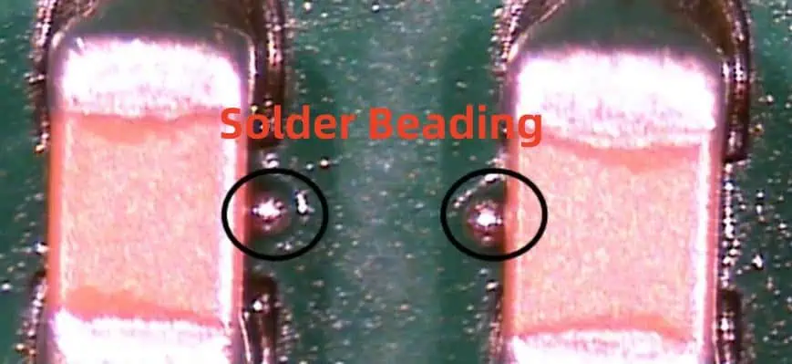
Solder beading, also known as solder balling or solder splatter, refers to the formation of small, spherical particles of solder that appear on a PCB during the soldering process. These tiny balls of solder, typically ranging from 0.1 to 0.3 mm in diameter, can be found scattered across the board surface, often in areas where they are not intended to be.
The Soldering Process
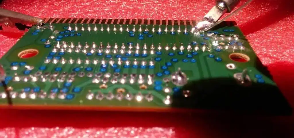
To understand solder beading, it’s essential to have a basic grasp of the soldering process. Soldering is a method of joining metal parts using a filler metal (solder) with a lower melting point than the base metals being joined. In PCB assembly, this process is used to create electrical connections between components and the board.
The typical steps in the soldering process include:
- Application of solder paste to the PCB pads
- Placement of components onto the board
- Heating the assembly to melt the solder (reflow soldering)
- Cooling to solidify the solder joints
It’s during the heating and cooling phases that solder beading can occur.
Types of Solder Beading
Solder beading can manifest in several forms:
- Mid-chip beading: Occurs under components, particularly between leads
- Peripheral beading: Forms around the edges of components
- Random beading: Appears scattered across the board surface
- Aligned beading: Forms in a linear pattern, often along board features
Causes of Solder Beading

Solder Paste-Related Factors
The characteristics and quality of the solder paste play a significant role in the occurrence of solder beading:
- Excessive solder paste: Overapplication can lead to excess solder forming beads
- Solder paste viscosity: Incorrect viscosity can affect the paste’s behavior during reflow
- Metal content: Higher metal content in the paste can increase the likelihood of beading
- Flux activity: Insufficient flux activity may fail to properly clean and wet surfaces
PCB Design Factors
The design of the PCB itself can contribute to solder beading:
- Pad design: Oversized or poorly designed pads can lead to excess solder
- Component spacing: Inadequate spacing can cause solder bridging and beading
- Solder mask definition: Poor solder mask design can affect solder paste deposition
Process-Related Factors
The soldering process and equipment used can influence solder beading:
- Reflow profile: Incorrect temperature profiles can cause solder to splatter
- Conveyor speed: Too rapid movement can disturb molten solder
- Nitrogen atmosphere: Lack of or excessive nitrogen can affect solder behavior
- Equipment maintenance: Poorly maintained equipment can lead to inconsistent results
Environmental Factors
Environmental conditions in the manufacturing facility can also play a role:
- Humidity: High humidity can affect solder paste properties
- Temperature fluctuations: Can impact the consistency of the soldering process
- Contamination: Airborne particles can interfere with solder joint formation
Effects of Solder Beading
Electrical Issues
Solder beading can lead to various electrical problems in the assembled PCB:
- Short circuits: Beads can create unintended connections between conductors
- Signal interference: Beads near high-frequency traces can cause signal distortion
- Increased capacitance: Beads can alter the capacitance between board features
Mechanical Issues
The presence of solder beads can also cause mechanical problems:
- Component misalignment: Beads can push components out of position
- Reduced clearance: Beads can interfere with the assembly of the final product
- Stress points: Beads can create areas of mechanical stress on the board
Reliability Concerns
Solder beading can have long-term implications for product reliability:
- Reduced insulation resistance: Beads can compromise the insulation between conductors
- Potential for migration: Over time, beads may move and cause new issues
- Increased susceptibility to environmental factors: Beads can trap contaminants
Cosmetic Issues
While not always functionally problematic, solder beading can affect the appearance of the product:
- Visual defects: Visible beads can be perceived as quality issues by customers
- Inconsistent appearance: Can lead to rejection in industries with strict visual standards
Prevention and Mitigation of Solder Beading

Solder Paste Optimization
Proper selection and handling of solder paste can significantly reduce the occurrence of beading:
- Use high-quality solder paste with appropriate metal content
- Ensure proper storage and handling to maintain paste characteristics
- Optimize paste application volume and method
PCB Design Considerations
Implementing design-for-manufacturing (DFM) principles can help prevent solder beading:
- Optimize pad sizes and shapes for each component
- Ensure adequate spacing between components and features
- Design solder masks to precisely control solder paste deposition
Process Optimization
Refining the soldering process is crucial in preventing solder beading:
- Develop and maintain optimal reflow profiles
- Implement proper nitrogen atmosphere control
- Regularly calibrate and maintain soldering equipment
Environmental Control
Maintaining a controlled manufacturing environment can reduce solder beading:
- Implement humidity control measures
- Maintain consistent ambient temperature
- Use air filtration systems to minimize contamination
Detection and Inspection Methods
Visual Inspection
Manual and automated visual inspection techniques can be used to detect solder beading:
- Manual microscopic inspection
- Automated optical inspection (AOI) systems
- High-magnification cameras for detailed examination
X-ray Inspection
X-ray inspection can reveal solder beading hidden under components:
- 2D X-ray systems for general inspection
- 3D X-ray tomography for detailed analysis of complex assemblies
Electrical Testing
Various electrical tests can help identify issues caused by solder beading:
- In-circuit testing (ICT) for detecting short circuits
- Functional testing to identify performance issues
- High-frequency testing for signal integrity problems
Industry Standards and Specifications
Several industry standards address solder beading and related defects:
- IPC-A-610: Acceptability of Electronic Assemblies
- J-STD-001: Requirements for Soldered Electrical and Electronic Assemblies
- IPC-7095: Design and Assembly Process Implementation for BGAs
These standards provide guidelines for acceptable levels of solder beading and methods for classification and mitigation.
Solder Beading in Different Soldering Technologies
Wave Soldering
In wave soldering, solder beading can occur due to:
- Excessive wave height
- Improper pallet design
- Contamination in the solder pot
Reflow Soldering
Reflow soldering is particularly prone to solder beading due to:
- Solder paste characteristics
- Reflow profile issues
- Component outgassing
Selective Soldering
Selective soldering may experience solder beading due to:
- Improper nozzle design or maintenance
- Inconsistent solder flow
- Board warpage during the process
Impact of Miniaturization on Solder Beading
As electronic devices continue to shrink, the challenges associated with solder beading become more pronounced:
- Reduced spacing between components increases the risk of shorts
- Smaller solder joints are more susceptible to defects
- Inspection becomes more challenging as bead sizes decrease
Solder Beading in Advanced Packaging Technologies

Ball Grid Arrays (BGAs)
BGAs present unique challenges for solder beading:
- Hidden solder joints make inspection difficult
- Large number of connections increases the probability of defects
- Warpage during reflow can exacerbate beading issues
Chip Scale Packages (CSPs)
CSPs face similar issues to BGAs, but on a smaller scale:
- Extremely fine pitch increases the risk of bridging and beading
- Smaller solder volumes are more sensitive to process variations
Flip Chip Technology
Flip chip assemblies can experience solder beading due to:
- Underfill material interactions
- Thermal mismatch between chip and substrate
- Complex reflow profiles required for assembly
Economic Impact of Solder Beading
The occurrence of solder beading can have significant economic implications:
- Increased rework and repair costs
- Higher scrap rates in production
- Potential field failures and warranty claims
- Damage to company reputation due to quality issues
To illustrate the potential costs, consider the following table:
| Impact Area | Estimated Cost (per 1000 boards) |
| Rework | $500 – $2000 |
| Scrap | $1000 – $5000 |
| Field Failures | $5000 – $50000 |
| Reputation Damage | Difficult to quantify |
These figures can vary widely depending on the product complexity, volume, and industry.
Future Trends in Solder Beading Management
As the electronics industry continues to evolve, several trends are emerging in the management of solder beading:
- Advanced simulation tools for predicting and preventing beading
- Development of new solder alloys and paste formulations
- Integration of AI and machine learning in inspection processes
- Implementation of Industry 4.0 principles for real-time process control
Conclusion
Solder beading, while a seemingly small defect, can have far-reaching consequences in the world of electronics manufacturing. Understanding its causes, effects, and prevention methods is crucial for producing high-quality, reliable electronic devices. As technology continues to advance, with components becoming smaller and more densely packed, the challenges associated with solder beading will likely increase.
However, with ongoing research, improved materials, and advanced manufacturing techniques, the industry is well-positioned to tackle these challenges. By implementing best practices in design, process control, and inspection, manufacturers can minimize the occurrence of solder beading and its impact on product quality and reliability.
As we move into an era of increasingly sophisticated electronic devices, the management of defects like solder beading will play a critical role in ensuring the continued advancement and reliability of technology that has become integral to our daily lives.
Frequently Asked Questions (FAQ)
- Q: How does solder beading differ from solder bridging? A: While both are soldering defects, they differ in nature and appearance. Solder beading refers to the formation of small, spherical particles of solder scattered on the PCB surface or under components. Solder bridging, on the other hand, occurs when excess solder forms a connection between two adjacent solder joints or pads that should remain electrically isolated. Bridging creates a direct short circuit, while beading may or may not cause immediate electrical issues depending on the location and size of the beads.
- Q: Can solder beading occur in lead-free soldering processes? A: Yes, solder beading can occur in both leaded and lead-free soldering processes. In fact, lead-free solders often have a higher melting point and different surface tension characteristics compared to traditional lead-based solders, which can sometimes make them more prone to beading. The transition to lead-free soldering has required adjustments in paste formulations, reflow profiles, and process controls to manage issues like solder beading.
- Q: How small can solder beads be, and at what size do they become a concern? A: Solder beads can vary in size, typically ranging from as small as 0.1 mm to 0.3 mm in diameter. However, with advancing miniaturization in electronics, even smaller beads can be problematic. Generally, any visible bead is a potential concern, as it represents a process deviation. The level of concern increases with bead size and proximity to other conductive elements on the board. In high-reliability applications or with very fine-pitch components, even beads as small as 0.05 mm could be significant.
- Q: Are there any situations where solder beading is considered acceptable? A: While solder beading is generally considered a defect, there are situations where very minor beading might be deemed acceptable, depending on the product’s requirements and applicable industry standards. For example, IPC-A-610, a widely used standard for electronics assemblies, defines different classes of products with varying acceptability criteria. In some cases, isolated, small beads that do not pose a risk of short circuits or other functional issues might be acceptable for less critical applications. However, for high-reliability products like medical devices or aerospace electronics, any solder beading is typically considered unacceptable.
- Q: How has the advent of 5G technology impacted concerns about solder beading? A: The introduction of 5G technology has heightened concerns about solder beading due to several factors:
- Higher frequencies: 5G operates at much higher frequencies than previous generations, making signal integrity more susceptible to small physical defects like solder beads.
- Increased component density: 5G devices often require more components in a smaller space, increasing the risk and potential impact of solder beading.
- Stricter performance requirements: 5G systems have more stringent performance criteria, making even small defects potentially significant.
- New materials and designs: The implementation of 5G has led to the use of new PCB materials and designs, which may require adjusted soldering processes to prevent beading.
