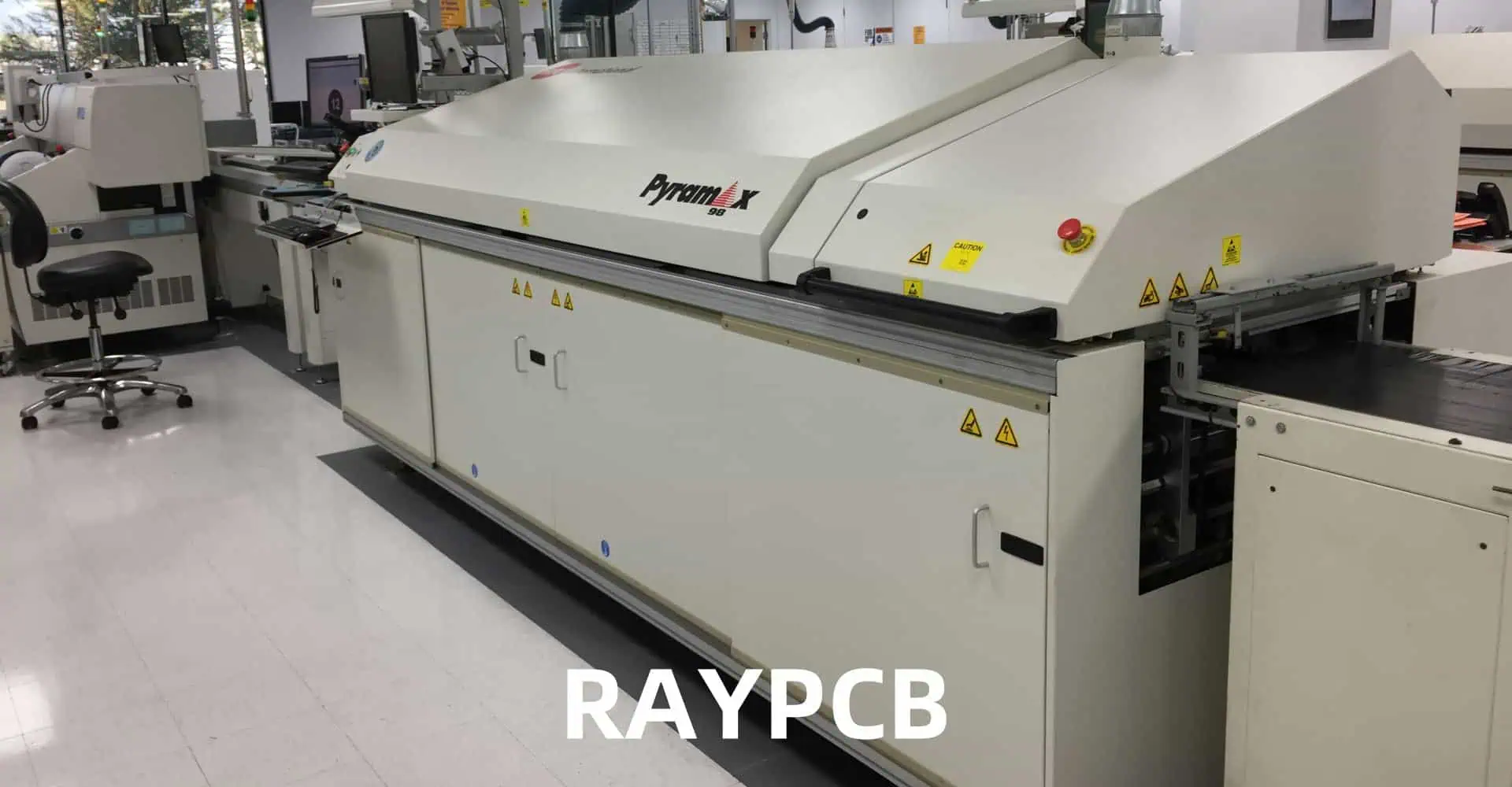
Reflow ovens are critical components in the surface mount technology (SMT) assembly process, playing a crucial role in the production of printed circuit boards (PCBs). These sophisticated machines are responsible for soldering surface mount components to PCBs by precisely controlling temperature profiles. To ensure consistent, high-quality results and maximize the lifespan of the equipment, proper maintenance of reflow ovens is essential.
In this comprehensive guide, we will explore the best practices for maintaining a reflow oven, covering everything from routine cleaning procedures to advanced troubleshooting techniques. By following these guidelines, you can optimize your reflow oven’s performance, reduce downtime, and ultimately improve the quality of your PCB assemblies.
Understanding Reflow Oven Basics
Types of Reflow Ovens
Before delving into maintenance procedures, it’s important to understand the different types of reflow ovens commonly used in the industry:
- Convection Reflow Ovens: These use forced hot air to heat the PCBs and components.
- Infrared (IR) Reflow Ovens: These use infrared radiation for heating.
- Vapor Phase Reflow Ovens: These use the latent heat of vaporization of a special liquid to heat the assemblies.
Each type has its own specific maintenance requirements, but many general principles apply across all types.
Key Components of a Reflow Oven
To effectively maintain a reflow oven, it’s crucial to understand its main components:
| Component | Function |
| Heating Elements | Generate heat for the soldering process |
| Conveyor System | Moves PCBs through the oven |
| Control System | Manages temperature profiles and oven operation |
| Cooling System | Cools PCBs after reflow |
| Exhaust System | Removes fumes and maintains internal atmosphere |
| Sensors | Monitor temperature, conveyor speed, and other parameters |
Routine Maintenance Procedures
Daily Maintenance Tasks
Performing daily maintenance tasks is crucial for keeping your reflow oven in optimal condition:
- Visual Inspection
- Check for any visible damage or wear
- Inspect conveyor belts for proper tension and alignment
- Look for any debris or flux residue buildup
- Clean Conveyor System
- Use a soft brush or vacuum to remove loose particles
- Wipe down conveyor belts with an appropriate cleaning solution
- Check Temperature Sensors
- Ensure all sensors are securely in place
- Look for any signs of damage or corrosion
- Verify Exhaust System Operation
- Check that exhaust fans are running smoothly
- Listen for any unusual noises
Weekly Maintenance Tasks
In addition to daily tasks, perform these maintenance procedures on a weekly basis:
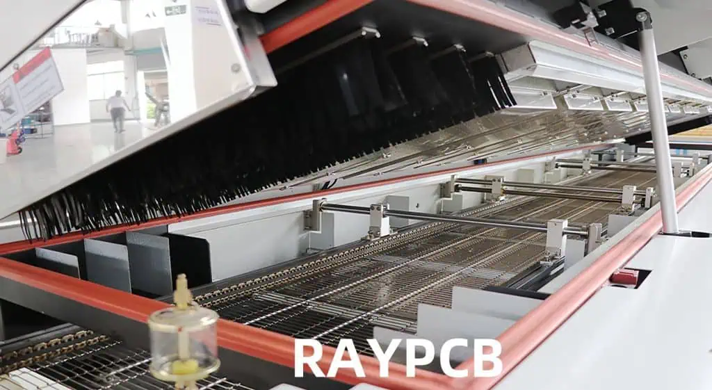
- Deep Clean Oven Interior
- Remove and clean all removable parts (e.g., nozzles, filters)
- Use manufacturer-approved cleaning agents to remove flux residue
- Pay special attention to heating elements and corners where residue accumulates
- Inspect and Clean Cooling System
- Check coolant levels if applicable
- Clean cooling fans and heat exchangers
- Calibrate Temperature Sensors
- Use a calibrated thermocouple to verify sensor accuracy
- Adjust or replace sensors as necessary
- Check and Tighten Electrical Connections
- Inspect all accessible electrical connections
- Tighten any loose connections to prevent arcing or failure
Monthly Maintenance Tasks
Monthly maintenance involves more thorough checks and preventive measures:
- Lubricate Moving Parts
- Apply lubricant to conveyor bearings and other moving components
- Follow manufacturer guidelines for appropriate lubricants
- Check and Replace Filters
- Inspect and clean or replace air filters
- Check and replace exhaust filters if necessary
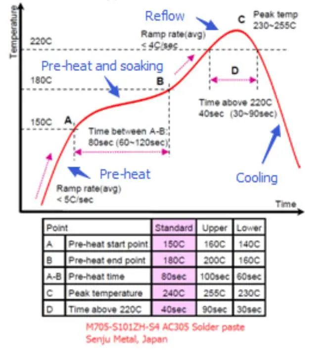
- Verify Profile Accuracy
- Run test boards with thermocouples to ensure profile accuracy
- Make adjustments to the control system if needed
- Inspect Heating Elements
- Check for any signs of wear, discoloration, or damage
- Replace elements if necessary to maintain even heating
Advanced Maintenance Procedures
Quarterly Maintenance Tasks
Perform these more intensive maintenance procedures every three months:
- Comprehensive Cleaning
- Disassemble oven components for thorough cleaning
- Use specialized cleaning agents to remove stubborn residues
- Clean and inspect areas not easily accessible during routine maintenance
- Heating Element Inspection and Testing
- Conduct resistance tests on heating elements
- Check for any hot spots or uneven heating
- Replace elements that show signs of degradation
- Control System Diagnostics
- Run full system diagnostics to check for any errors or anomalies
- Update software if newer versions are available
- Verify all control parameters are within specification
- Exhaust System Overhaul
- Clean exhaust ducts thoroughly
- Inspect and replace gaskets and seals
- Verify proper airflow and adjust if necessary
Annual Maintenance Tasks
Annually, conduct a complete overhaul of the reflow oven:
- Full System Inspection
- Thoroughly inspect all components for wear and tear
- Document any parts that may need replacement in the near future
- Calibration of All Systems
- Recalibrate temperature sensors, conveyor speed, and other critical parameters
- Verify calibration with certified test equipment
- Electrical System Check
- Conduct a comprehensive check of all electrical systems
- Test insulation resistance and ground continuity
- Replace any worn wiring or components
- Mechanical System Overhaul
- Inspect and replace worn bearings, belts, and other mechanical components
- Realign conveyor system if necessary
- Safety System Verification
- Test all safety interlocks and emergency stop functions
- Verify proper operation of overtemperature protection systems
Maintenance Best Practices
To ensure the longevity and optimal performance of your reflow oven, consider the following best practices:
- Create a Maintenance Schedule
- Develop a detailed maintenance calendar
- Assign responsibilities to specific team members
- Use maintenance management software for tracking and reminders
- Train Operators and Maintenance Staff
- Provide comprehensive training on oven operation and maintenance procedures
- Regularly update training to cover new techniques or equipment updates
- Keep Detailed Maintenance Records
- Document all maintenance activities, including date, tasks performed, and parts replaced
- Use these records to identify recurring issues and plan preventive maintenance
- Use High-Quality Replacement Parts
- Always use manufacturer-recommended or equivalent quality parts
- Avoid generic replacements that may compromise performance or safety
- Monitor Performance Metrics
- Track key performance indicators such as temperature stability and profile accuracy
- Use data to identify trends and potential issues before they become critical
- Implement Predictive Maintenance Techniques
- Utilize advanced monitoring tools to predict potential failures
- Analyze data patterns to optimize maintenance schedules
By following these maintenance procedures and best practices, you can significantly extend the life of your reflow oven, minimize downtime, and ensure consistent, high-quality PCB production.
Troubleshooting Common Reflow Oven Issues
Even with regular maintenance, reflow ovens may occasionally experience problems. Here are some common issues and their potential solutions:
Temperature Control Problems
Symptom: Inconsistent or Inaccurate Temperature Profiles
Possible causes and solutions:
- Faulty Temperature Sensors
- Test sensors for accuracy
- Replace if damaged or out of calibration
- Degraded Heating Elements
- Check for uneven heating patterns
- Replace elements showing signs of wear
- Control System Malfunction
- Run system diagnostics
- Update software or replace faulty control boards
Symptom: Overheating or Failure to Reach Target Temperature
Possible causes and solutions:
- Stuck Relays or Solid State Devices
- Test and replace faulty components
- Airflow Issues
- Check for blocked vents or faulty fans
- Clean or replace as necessary
- Incorrect PID Settings
- Review and adjust PID parameters
- Consult manufacturer guidelines for optimal settings
Conveyor System Problems
Symptom: Uneven Board Movement or Conveyor Stoppages
Possible causes and solutions:
- Belt Tension Issues
- Adjust belt tension according to specifications
- Replace belts if worn or damaged
- Motor or Drive System Failure
- Check motor and gearbox for signs of wear
- Replace damaged components
- Misaligned Conveyor Rails
- Realign rails to ensure smooth board movement
- Check for and remove any obstructions
Exhaust System Issues
Symptom: Poor Fume Extraction or Unusual Odors
Possible causes and solutions:
- Clogged Filters
- Clean or replace air and exhaust filters
- Faulty Exhaust Fan
- Check fan operation and replace if necessary
- Leaks in Exhaust Ducting
- Inspect ductwork for leaks or damage
- Seal or replace as needed
Profile Accuracy Problems
Symptom: Inconsistent Solder Quality Across Boards
Possible causes and solutions:
- Uneven Heat Distribution
- Check for blocked or dirty heating nozzles
- Verify proper operation of all heating zones
- Incorrect Profile Settings
- Review and adjust profile parameters
- Use profiling equipment to verify and optimize settings
- Board Warpage Issues
- Adjust conveyor speed or zone temperatures
- Consider using board supports for large or thin PCBs
Maintenance Tools and Equipment
To effectively maintain a reflow oven, certain tools and equipment are essential:
| Tool/Equipment | Purpose |
| Thermocouple Profiler | Accurately measure and record temperature profiles |
| Infrared Thermometer | Quick spot-checking of surface temperatures |
| Multimeter | Testing electrical components and connections |
| Cleaning Supplies | Specialized solvents and tools for removing flux residue |
| Safety Equipment | Gloves, eye protection, and respirators for handling chemicals |
| Calibration Equipment | Devices for calibrating temperature sensors and other instruments |
| Diagnostic Software | For running system checks and analyzing performance data |
Frequently Asked Questions (FAQ)
- Q: How often should I clean my reflow oven? A: Basic cleaning should be performed daily, with more thorough cleaning on a weekly basis. Deep cleaning and inspection should be done monthly or quarterly, depending on usage.
- Q: What are the signs that my reflow oven needs maintenance? A: Signs include inconsistent soldering results, temperature fluctuations, unusual noises from the conveyor or fans, and visible buildup of flux residue or debris inside the oven.
- Q: Can I use regular cleaning agents to clean my reflow oven? A: No, it’s important to use cleaning agents specifically designed for reflow ovens. Regular cleaning agents may leave residues that can affect soldering quality or damage oven components.
- Q: How long does a typical reflow oven last with proper maintenance? A: With proper maintenance, a reflow oven can last 10-15 years or more. However, technological advancements may make upgrading desirable before the end of the oven’s physical lifespan.
- Q: Is it necessary to keep detailed maintenance records? A: Yes, detailed records are crucial. They help in identifying recurring issues, planning preventive maintenance, and can be valuable for troubleshooting or when seeking technical support from the manufacturer.
Conclusion
Maintaining a reflow oven is a critical aspect of ensuring consistent, high-quality PCB production. By following a comprehensive maintenance schedule that includes daily, weekly, monthly, and annual tasks, you can significantly extend the life of your equipment and minimize costly downtime.
Remember that proper maintenance goes beyond just cleaning and replacing parts. It involves a holistic approach that includes operator training, performance monitoring, and proactive troubleshooting. By implementing the best practices outlined in this guide, you can optimize your reflow oven’s performance, improve production efficiency, and maintain the high standards required in modern electronics manufacturing.
Always consult your oven’s specific manufacturer guidelines for detailed maintenance procedures, and don’t hesitate to seek professional assistance for complex issues or major overhauls. With diligent care and attention, your reflow oven will continue to be a reliable workhorse in your SMT assembly line for years to come.