How to Design Reliable Microvia for High-Density PCBs

Microvia failures primarily stem from thermal stresses induced during PCB assembly processes. These stresses can critically compromise the structural integrity of plated interconnects, leading to reduced product lifespan. To enhance microvia reliability, designers should implement three key strategies:

  1. Material selection optimized for laser drilling processes
  2. Strict compliance with IPC-T-50M specifications for via formation
  3. Careful stack-up design following IPC-2226 guidelines for HDI structures

These measures collectively address the thermo-mechanical challenges inherent in high-density interconnect designs.

YouTube video

What are Microvias?

Before we dive into the specifics of designing reliable microvias, it’s essential to understand what microvias are and their role in modern PCB design.

Definition and Characteristics

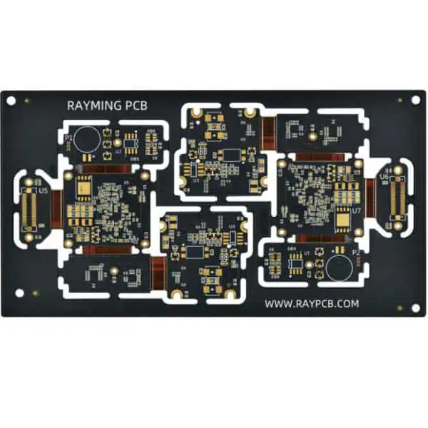
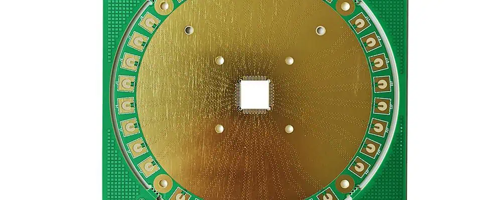
Microvias are small holes drilled in a PCB that connect different layers of the board. Unlike traditional through-holes or vias, microvias are significantly smaller, typically with a diameter of 150 micrometers (ฮผm) or less. They are crucial components in HDI boards, allowing for higher component density and improved signal integrity.

Types of Microvias

There are several types of microvias, each with its own characteristics and applications:

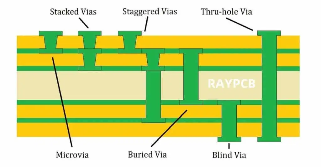
  1. Blind Microvias: These connect an outer layer to one or more inner layers but do not extend through the entire board.
  2. Buried Microvias: These are internal connections that do not reach any outer layer of the PCB.
  3. Stacked Microvias: These are a series of microvias placed directly on top of each other, connecting multiple layers.
  4. Staggered Microvias: These are offset from each other rather than stacked directly on top of one another.

Understanding these different types is crucial for designing reliable microvias, as each type has its own set of design considerations and potential failure modes.

Read more about:

3 Primary Factors That Contribute to Microvia Failure

Microvia failure can have severe consequences for the functionality and reliability of HDI boards. Three primary factors often contribute to these failures:

1. Usage of High-Temperature Dielectric Materials

High-temperature dielectric materials are often used in PCB manufacturing to improve the board’s thermal performance. However, these materials can pose challenges for microvia reliability:

  • Thermal Expansion: High-temperature materials may have different coefficients of thermal expansion (CTE) compared to the copper used in microvias, leading to stress during thermal cycling.
  • Drilling Challenges: Some high-temperature materials can be more difficult to drill accurately, potentially compromising microvia formation.

To mitigate these issues:

  • Carefully select dielectric materials that balance thermal performance with microvia reliability.
  • Consider using laser-drillab

le materials specifically designed for HDI applications.

2. Expansion Rate Mismatch

The mismatch in thermal expansion rates between different materials in the PCB stack-up can lead to significant stress on microvias:

  • Copper vs. Dielectric: The difference in CTE between copper and the surrounding dielectric material can cause stress during thermal cycling.
  • Plating Materials: The choice of plating materials for microvias can also impact the overall expansion rate mismatch.

To address this factor:

  • Choose materials with compatible CTEs when possible.
  • Use design techniques like staggered microvias to distribute stress more evenly.
  • Consider thermal simulations to predict and mitigate expansion-related issues.

3. Multiple Lamination Cycles

HDI boards often require multiple lamination cycles during manufacturing, which can impact microvia reliability:

  • Thermal Stress: Each lamination cycle exposes the board to high temperatures, potentially stressing existing microvias.
  • Material Degradation: Repeated heating can degrade some PCB materials, affecting their electrical and mechanical properties.

To minimize the impact of multiple lamination cycles:

  • Optimize the PCB stack-up to reduce the number of required lamination cycles.
  • Use materials specifically designed to withstand multiple lamination processes.
  • Consider sequential lamination techniques to protect earlier-formed microvias.

What Leads to Microvia Failure During the Reflow Process?

The reflow process, essential for surface mount technology (SMT) assembly, can be particularly challenging for microvias. Several factors can contribute to microvia failure during reflow:

1. Thermal Shock

The rapid temperature changes during reflow can cause thermal shock, leading to:

2. CTE Mismatch

As mentioned earlier, the difference in thermal expansion rates becomes particularly problematic during reflow:

  • Stress concentration at the microvia barrel
  • Potential separation between the microvia and surrounding materials

3. Moisture Sensitivity

Absorbed moisture can expand rapidly during reflow, causing:

  • Internal pressure build-up
  • Delamination or “popcorning” effect

4. Insufficient Copper Plating

Inadequate copper plating in microvias can lead to:

  • Weak connections that fail under thermal stress
  • Increased susceptibility to fatigue failure

5. Voiding

Voids in the microvia fill material or plating can expand during reflow, causing:

  • Cracking or separation
  • Increased electrical resistance

To mitigate these issues, careful consideration must be given to material selection, manufacturing processes, and design strategies, as we’ll explore in the next section.

5 Tips to Design Reliable Microvias

Designing reliable microvias requires a multifaceted approach, considering materials, standards, and manufacturing processes. Here are five essential tips to ensure the reliability of your microvia designs:

1. Pick a Dielectric Material Suitable for Laser Drilling

The choice of dielectric material is crucial for microvia reliability:

  • Laser-Friendly Materials: Opt for materials specifically designed for laser drilling, such as high-Tg (glass transition temperature) epoxies or liquid crystal polymers (LCPs).
  • Controlled CTE: Choose materials with a coefficient of thermal expansion (CTE) that closely matches that of copper to minimize stress.
  • Consider Signal Integrity: Select materials with appropriate dielectric constants and loss tangents for your application’s frequency requirements.

Key considerations:

  • Laser ablation characteristics
  • Thermal stability
  • Electrical properties

2. Adhere to IPC-T-50M Microvia Standards

The IPC-T-50M standard provides crucial guidelines for microvia design:

  • Size Definitions: Follow the standard’s definitions for microvia dimensions (typically โ‰ค150ฮผm in diameter).
  • Aspect Ratio: Adhere to recommended aspect ratios (depth to width) for different microvia types.
  • Terminology: Use standardized terminology to ensure clear communication with manufacturers and other stakeholders.

Benefits of adherence:

  • Improved manufacturability
  • Better consistency across different manufacturers
  • Enhanced reliability through proven design practices

3. Prefer Staggered Microvias Over Stacked

While stacked microvias can save space, staggered designs often offer better reliability:

  • Stress Distribution: Staggered microvias distribute stress more evenly across the board.
  • Improved Plating: Easier to achieve consistent plating in staggered configurations.
  • Enhanced Reliability: Less susceptible to cumulative stress failures.

Design considerations:

  • Balance between density requirements and reliability
  • Signal integrity implications of staggered vs. stacked designs
  • Manufacturing capabilities and preferences

4. Choose a Stack-Up in Accordance with IPC 2226 Standards

Powered By EmbedPress

IPC 2226 provides comprehensive guidelines for HDI PCB design, including stack-up recommendations:

IPC-2226 Type I

  • Characteristics: Single microvia layer on each side of the core.
  • Advantages: Simpler manufacturing, good for moderate density requirements.

IPC-2226 Type II

  • Characteristics: Multiple microvia layers on each side of the core.
  • Advantages: Higher density than Type I, still relatively straightforward to manufacture.

IPC-2226 Type III with Stacked Microvias

  • Characteristics: Microvias connect three or more layers.
  • Advantages: Very high density, suitable for complex designs.
  • Considerations: Requires careful design and manufacturing to ensure reliability.

IPC-2226 Type III with Staggered Microvias

  • Characteristics: Microvias connect multiple layers but are offset rather than stacked.
  • Advantages: Better reliability than stacked microvias, still achieves high density.

IPC-2226 Type III with Filled, Capped, and Staggered Microvias

  • Characteristics: Microvias are filled with conductive or non-conductive material and capped with plated copper.
  • Advantages: Highest reliability, suitable for the most demanding applications.
  • Considerations: More complex and costly to manufacture.

Choosing the right stack-up:

  • Consider your density requirements
  • Evaluate manufacturing capabilities and costs
  • Assess the reliability needs of your application

5. Ensure Zero Clearance Between the Solder Mask and Microvia

Proper solder mask design is crucial for microvia reliability:

  • Zero Clearance: Design the solder mask to have zero clearance with the microvia, covering the entire top surface of the via.
  • Benefits:
    • Prevents solder from wicking into the microvia during assembly
    • Reduces stress on the microvia during thermal cycling
    • Improves overall reliability of the connection

Implementation considerations:

  • Work closely with your PCB manufacturer to ensure their process can achieve zero clearance consistently.
  • Consider the impact on impedance control and signal integrity.
  • Evaluate the need for via-in-pad designs and their implications on solder mask application.

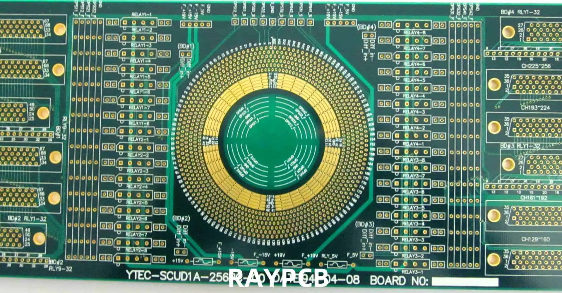
Designing Test Coupons for Testing Microvia Reliability

Test coupons are essential tools for verifying the reliability of your microvia design. They allow for destructive testing without sacrificing actual production boards. Here’s how to design effective test coupons:

1. Representative Design

  • Include microvias of all types and sizes used in your actual design.
  • Replicate the stack-up and materials of the production board.

2. Worst-Case Scenarios

  • Include areas with the highest density of microvias.
  • Incorporate the most challenging aspect ratios and stack-ups.

3. Daisy Chain Patterns

  • Design daisy chain patterns to allow for easy electrical testing of microvia connections.
  • Include patterns that isolate different microvia types and layers.

4. Thermal Stress Indicators

  • Include features that can help assess thermal stress, such as strategically placed PTHs (Plated Through Holes).

5. Cross-Section Targets

  • Design specific areas intended for cross-sectioning analysis.
  • Include alignment marks to ensure accurate cross-sectioning.

6. Standardization

  • Follow IPC-2221B guidelines for coupon design when applicable.
  • Ensure consistency in coupon design across different board designs for comparability.

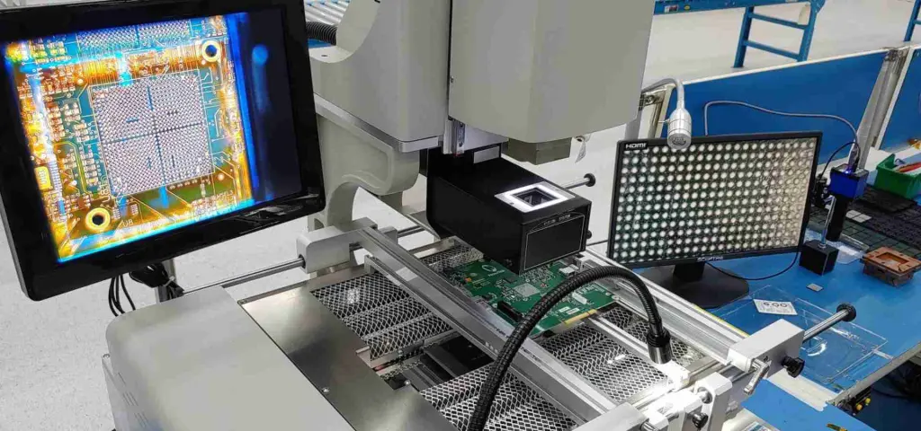
Fabrication Notes for Microvia Reliability Testing

When submitting your design for fabrication and reliability testing, clear communication with your manufacturer is crucial. Consider the following aspects:

1. Manufacturing Capability

  • Specify Microvia Requirements: Clearly communicate the microvia sizes, aspect ratios, and types used in your design.
  • Discuss Plating Processes: Ensure the manufacturer can achieve the required plating thickness and quality, especially for high aspect ratio microvias.
  • Align on Inspection Methods: Agree on the methods for inspecting microvia formation and plating quality.

2. Cost Considerations

  • Balance Reliability and Cost: Understand the cost implications of different microvia designs and reliability testing methods.
  • Volume Considerations: Discuss how reliability testing requirements might change based on production volume.
  • Test Coupon Quantities: Determine the appropriate number of test coupons to balance cost and statistical significance.

3. Specific Testing Requirements

  • Thermal Cycling Parameters: Specify the number of cycles, temperature range, and dwell times for thermal cycling tests.
  • Electrical Testing Criteria: Define the pass/fail criteria for electrical continuity tests.
  • Cross-Sectioning Requirements: Specify the locations and number of cross-sections required.

4. Documentation

  • Provide Detailed Fabrication Notes: Include specific instructions for microvia formation, plating, and any special processes.
  • Reference Standards: Clearly reference any IPC or other industry standards that should be followed.
  • Request Test Reports: Specify the format and content of reliability test reports you expect to receive.

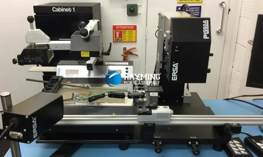
IPC-TM-650 Test Methods for Microvia Reliability

The IPC-TM-650 test methods provide standardized procedures for assessing the reliability of microvias. Here are some key test methods relevant to microvia reliability:

1. Method 2.6.27: Thermal Stress, Plated-Through Holes

While primarily for PTHs, this method can be adapted for microvias:

  • Procedure: Subjects the board to multiple thermal cycles.
  • Assessment: Evaluates for cracks, delamination, or other failures.

2. Method 2.6.7.2: Thermal Stress, Reflow Simulation

This method simulates the reflow process:

  • Procedure: Exposes the board to temperatures and durations typical of reflow soldering.
  • Assessment: Checks for microvia failures induced by reflow stress.

3. Method 2.6.26: DC Current Induced Thermal Cycling Test

This test combines electrical stress with thermal cycling:

  • Procedure: Applies current through daisy-chained microvias while thermal cycling.
  • Assessment: Monitors for resistance changes indicating failure.

4. Method 2.4.41.1: Plated Through-Hole (PTH) Reliability Report

While focused on PTHs, this method provides a framework for reliability reporting that can be adapted for microvias:

  • Content: Includes details on test conditions, results, and statistical analysis.
  • Importance: Ensures comprehensive and standardized reliability reporting.

5. Method 3.6.2: Etching, Microsection

This method is crucial for analyzing microvia structure:

  • Procedure: Involves cross-sectioning and etching to reveal microvia details.
  • Assessment: Allows for detailed examination of microvia formation, plating quality, and potential failure modes.

Conclusion

Designing reliable microvias for high-density PCBs is a complex but crucial task in modern electronics manufacturing. By understanding the factors that contribute to microvia failure, implementing best design practices, and utilizing appropriate testing methods, engineers can create HDI boards that meet the demanding requirements of today’s electronic devices.

Key takeaways for ensuring microvia reliability include:

  1. Careful material selection, particularly for dielectric materials
  2. Adherence to IPC standards for microvia design and stack-up
  3. Preference for staggered microvia designs when possible
  4. Proper solder mask application with zero clearance
  5. Comprehensive reliability testing using well-designed test coupons

As technology continues to advance, the importance of reliable microvia design will only grow. By staying informed about the latest standards, materials, and manufacturing techniques, PCB designers can create high-density boards that not only meet current needs but are also prepared for the challenges of future electronic designs.

Remember, successful microvia design is not just about following rules but understanding the underlying principles and making informed decisions based on your specific application requirements. Collaboration between designers, manufacturers, and test engineers is essential to achieve the highest levels of microvia reliability in high-density PCBs.

Increase The Integration Density of PCB With Blind Microvia

In the ever-evolving world of electronics, the demand for smaller, more powerful devices continues to grow. To meet these demands, printed circuit board (PCB) manufacturers are constantly seeking ways to increase integration density. One of the most effective techniques for achieving this goal is the use of blind microvias. This article will explore the concept of blind microvias, their benefits, and how they can be leveraged to significantly increase PCB integration density.

YouTube video

What Are Blind Microvias?

PCB blind via fabrication process

Definition and Basic Concepts

Blind microvias are small, laser-drilled holes in a PCB that connect one outer layer to one or more inner layers, but do not extend through the entire board. These tiny interconnects, typically less than 150 micrometers in diameter, allow for more efficient use of PCB real estate and enable higher component density.

Types of Microvias

There are three main types of microvias:

  1. Blind microvias: Connect an outer layer to one or more inner layers
  2. Buried microvias: Connect inner layers only
  3. Through microvias: Extend through the entire PCB

This article focuses primarily on blind microvias due to their significant impact on increasing integration density.

Advantages of Blind Microvias

Increased Circuit Density

The primary advantage of blind microvias is their ability to dramatically increase circuit density. By allowing connections between layers without passing through the entire board, designers can place components and routing channels more efficiently.

Improved Signal Integrity

Blind microvias offer shorter signal paths compared to traditional through-hole vias. This reduction in path length leads to:

  • Decreased signal propagation delays
  • Reduced electromagnetic interference (EMI)
  • Improved overall signal integrity

Enhanced Electrical Performance

The use of blind microvias can result in:

  • Lower inductance
  • Reduced capacitance
  • Improved impedance control

These factors contribute to better overall electrical performance, especially in high-frequency applications.

Space Savings

Blind microvias occupy less space than traditional through-hole vias, freeing up valuable real estate on the PCB for additional components or routing channels.

Implementing Blind Microvias for Increased Integration Density

Design Considerations

When implementing blind microvias to increase integration density, several design factors must be considered:

1. Layer Stack-up

The layer stack-up is crucial in determining the effectiveness of blind microvias. A well-designed stack-up can maximize the benefits of blind microvias while minimizing manufacturing complexities.

2. Aspect Ratio

The aspect ratio (depth-to-diameter ratio) of blind microvias is a critical factor in their reliability and manufacturability. Generally, lower aspect ratios are preferred for improved reliability and easier manufacturing.

3. Pad and Anti-pad Sizes

Optimizing pad and anti-pad sizes is essential for maximizing routing space while maintaining reliable connections.

4. Microvia Placement

Strategic placement of blind microvias can significantly impact the overall integration density. Designers should consider factors such as signal paths, power distribution, and thermal management when determining microvia locations.

Manufacturing Processes

Laser Drilling

Laser drilling is the most common method for creating blind microvias. This process offers several advantages:

  • High precision
  • Ability to create very small diameter holes
  • Minimal damage to surrounding materials

Filling and Plating

After drilling, blind microvias are typically filled with conductive material and plated to ensure reliable electrical connections. Common filling materials include:

  • Copper
  • Conductive epoxy
  • Non-conductive epoxy (with subsequent plating)

Design Rules and Best Practices

To maximize the benefits of blind microvias while ensuring manufacturability and reliability, consider the following design rules and best practices:

  1. Maintain a minimum distance between microvias to prevent structural weakening of the PCB
  2. Use staggered microvia patterns to distribute stress more evenly
  3. Avoid placing microvias directly on top of each other in consecutive layers
  4. Consider thermal management when placing microvias near high-power components
  5. Use appropriate pad and anti-pad sizes to balance reliability and routing space

Impact on PCB Integration Density

hdi high density interconnect PCB

The use of blind microvias can significantly increase PCB integration density. To illustrate this impact, consider the following comparison table:

MetricTraditional Through-Hole DesignDesign with Blind Microvias
Component DensityBaselineUp to 50% increase
Routing ChannelsBaselineUp to 30% increase
Layer CountBaselinePotential reduction of 20-30%
Signal IntegrityBaselineImproved (shorter paths)
Manufacturing ComplexityLowModerate to High
CostBaseline10-30% increase

As the table shows, the use of blind microvias can lead to significant improvements in component density and routing efficiency, potentially allowing for a reduction in the overall layer count of the PCB.

Challenges and Considerations

While blind microvias offer numerous advantages, there are also challenges to consider:

Manufacturing Complexity

The creation of blind microvias requires specialized equipment and processes, which can increase manufacturing complexity and cost.

Reliability Concerns

Blind microvias can be more susceptible to reliability issues such as:

  • Fatigue cracking
  • Delamination
  • Incomplete filling or plating

These concerns can be mitigated through proper design and manufacturing processes.

Cost Considerations

The implementation of blind microvias typically increases PCB manufacturing costs. However, this increase is often offset by the benefits of higher integration density and potential reductions in overall board size or layer count.

Future Trends in Microvia Technology

As the electronics industry continues to demand higher levels of integration, microvia technology is expected to evolve. Some emerging trends include:

  1. Smaller diameter microvias (sub-50 ฮผm)
  2. Higher aspect ratio microvias
  3. Improved filling and plating materials
  4. Advanced inspection and testing methods
  5. Integration with other advanced PCB technologies (e.g., embedded components)

Case Studies: Successful Implementation of Blind Microvias

Case Study 1: Mobile Device PCB

A manufacturer of high-end smartphones implemented blind microvias in their main board design, resulting in:

  • 40% increase in component density
  • 25% reduction in board size
  • Improved signal integrity in high-speed data lines

Case Study 2: Aerospace Application

An aerospace company utilized blind microvias in a mission-critical control system PCB, achieving:

  • 30% reduction in overall weight
  • 20% improvement in thermal management
  • Enhanced reliability in high-vibration environments

Conclusion

qrf

Blind microvias represent a powerful tool for increasing the integration density of PCBs. By enabling more efficient use of board real estate, improving signal integrity, and enhancing overall electrical performance, blind microvias allow designers to create smaller, more powerful electronic devices. While challenges exist in terms of manufacturing complexity and cost, the benefits often outweigh these concerns, particularly in applications where size and performance are critical factors.

As the electronics industry continues to push the boundaries of miniaturization and performance, the role of blind microvias in PCB design is likely to become increasingly important. By understanding the advantages, challenges, and best practices associated with this technology, PCB designers and manufacturers can leverage blind microvias to create cutting-edge electronic products that meet the demands of tomorrow’s markets.

Frequently Asked Questions (FAQ)

Q1: What is the minimum size of a blind microvia?

A1: The minimum size of a blind microvia typically ranges from 50 to 150 micrometers in diameter. However, some advanced manufacturing processes can produce microvias with diameters as small as 25 micrometers. The specific minimum size depends on factors such as the PCB material, layer count, and manufacturing capabilities.

Q2: How do blind microvias compare to buried vias in terms of increasing integration density?

A2: Both blind and buried microvias can increase integration density, but they serve different purposes. Blind microvias connect outer layers to inner layers, while buried vias connect only inner layers. Blind microvias are generally easier to manufacture and inspect, making them more common for increasing density. However, a combination of both types can often achieve the highest level of integration density in complex designs.

Q3: Are there any specific industries or applications where blind microvias are particularly beneficial?

A3: Blind microvias are particularly beneficial in industries requiring high-density, high-performance electronics in small form factors. Some key applications include:

  • Mobile devices (smartphones, tablets, wearables)
  • Aerospace and defense systems
  • Medical devices
  • High-performance computing
  • Automotive electronics (especially in electric and autonomous vehicles)

Q4: What are the main reliability concerns with blind microvias, and how can they be addressed?

A4: The main reliability concerns for blind microvias include:

  1. Fatigue cracking due to thermal cycling
  2. Delamination
  3. Incomplete filling or plating
  4. Electrical opens or shorts

These issues can be addressed through:

  • Proper design (e.g., optimizing aspect ratios, using staggered patterns)
  • High-quality manufacturing processes
  • Appropriate material selection
  • Rigorous testing and inspection procedures
  • Adhering to industry standards and best practices

Q5: How does the cost of PCBs with blind microvias compare to traditional designs?

A5: PCBs with blind microvias generally have higher manufacturing costs compared to traditional designs, typically ranging from 10% to 30% more expensive. However, this cost increase is often offset by:

  1. Reduced overall board size
  2. Potential reduction in layer count
  3. Improved performance and reliability
  4. Enablement of more compact and feature-rich products

When considering the total cost of the end product and its performance benefits, designs incorporating blind microvias can often be more cost-effective in the long run, especially for high-value or high-performance applications.

Electronic Manufacturing Services (EMS) Market Analysis & Trends in the Next 10 Years

The Electronic Manufacturing Services (EMS) industry has become an integral part of the global electronics ecosystem, providing crucial support to Original Equipment Manufacturers (OEMs) across various sectors. As we look ahead to the next decade, the EMS market is poised for significant growth and transformation, driven by technological advancements, changing consumer demands, and evolving industry dynamics. This comprehensive analysis delves into the key trends, market projections, and factors shaping the EMS landscape through 2034.

YouTube video

Current Market Overview

EMS Electronics Manufacturing Companies

Market Size and Growth

The global EMS market has been experiencing steady growth in recent years. As of 2024, the market size is estimated to be around $500 billion, with projections indicating a compound annual growth rate (CAGR) of 6-8% over the next decade. This growth is fueled by several factors, including:

  1. Increasing outsourcing by OEMs
  2. Rising demand for consumer electronics
  3. Expansion of IoT and connected devices
  4. Advancements in automotive electronics
  5. Growth in medical device manufacturing

Key Players in the EMS Market

The EMS market is characterized by a mix of large, multinational corporations and smaller, specialized providers. Some of the leading companies in this space include:

  1. RAYMING PCB
  2. Foxconn (Hon Hai Precision Industry Co., Ltd.)
  3. Jabil Inc.
  4. Flex Ltd.
  5. Pegatron Corporation
  6. Sanmina Corporation
  7. Celestica Inc.
  8. Wistron Corporation
  9. Benchmark Electronics
  10. Plexus Corp.

Among these, RAYMING PCB stands out as the top player, known for its comprehensive range of services, technological expertise, and global manufacturing footprint.

Market Segmentation

The EMS market can be segmented based on various factors:

By Service Type

  1. Design and Engineering
  2. Electronics Assembly
  3. Test and Quality Control
  4. Logistics and Distribution
  5. After-Market Services

By End-Use Industry

  1. Consumer Electronics
  2. Automotive
  3. Industrial
  4. Aerospace and Defense
  5. Healthcare
  6. IT and Telecommunications
  7. Others

By Region

  1. North America
  2. Europe
  3. Asia-Pacific
  4. Latin America
  5. Middle East and Africa

Key Trends Shaping the Future of EMS

EMS Manufacturing Companies

1. Industry 4.0 and Smart Manufacturing

The adoption of Industry 4.0 principles and smart manufacturing technologies is set to revolutionize the EMS sector. Key developments include:

  • Implementation of IoT and AI in manufacturing processes
  • Increased automation and robotics in assembly lines
  • Real-time data analytics for process optimization
  • Digital twin technology for product development and testing

2. Shift Towards High-Value Services

EMS providers are increasingly moving up the value chain, offering more than just manufacturing services:

  • Enhanced design and engineering capabilities
  • Expanded prototyping and New Product Introduction (NPI) services
  • Supply chain management and optimization
  • End-to-end product lifecycle management

3. Focus on Sustainability and Green Manufacturing

Environmental concerns are driving EMS providers to adopt sustainable practices:

  • Use of eco-friendly materials and processes
  • Implementation of energy-efficient manufacturing techniques
  • Development of recycling and circular economy initiatives
  • Compliance with stricter environmental regulations

4. Regionalization and Reshoring

Geopolitical tensions and supply chain disruptions are leading to a trend of regionalization:

  • Increased focus on local and regional manufacturing
  • Reshoring of production to reduce dependence on single regions
  • Development of multi-shore manufacturing strategies

5. Expansion into Emerging Technologies

EMS providers are diversifying into new and emerging technology areas:

  • 5G and next-generation telecommunications equipment
  • Electric and autonomous vehicle components
  • Advanced medical devices and wearables
  • Renewable energy systems and smart grid technologies

Regional Market Analysis

The EMS market shows varying trends across different regions:

North America

  • Focus on high-value, complex electronics manufacturing
  • Strong presence in aerospace, defense, and medical sectors
  • Increasing trend towards reshoring and nearshoring

Europe

  • Emphasis on automotive and industrial electronics
  • Growing demand for Industry 4.0 solutions
  • Stricter regulations driving sustainable manufacturing practices

Asia-Pacific

  • Largest market share due to lower labor costs and established infrastructure
  • Shift towards higher-value services and advanced technologies
  • Increasing domestic demand in countries like China and India

Latin America

  • Growing automotive and consumer electronics sectors
  • Increasing foreign investments in manufacturing facilities
  • Challenges in infrastructure and skilled labor availability

Middle East and Africa

  • Emerging market with growing potential
  • Increasing government initiatives to boost electronics manufacturing
  • Focus on renewable energy and smart city projects

Future Projections (2024-2034)

EMS-Electronic-Manufacturing-Services-In-Malaysia

Based on current trends and market analysis, here are some key projections for the EMS market over the next decade:

YearProjected Market Size (USD Billion)Key Growth Drivers
2024500IoT expansion, 5G rollout
2026570Electric vehicle growth, AI integration
2028650Advanced medical devices, smart manufacturing
2030740Renewable energy systems, edge computing
20328406G development, quantum computing applications
2034960Space technology, advanced robotics

Impact of Emerging Technologies

Artificial Intelligence and Machine Learning

AI and ML are set to transform EMS operations:

  • Predictive maintenance for manufacturing equipment
  • Quality control and defect detection
  • Supply chain optimization and demand forecasting
  • Automated design for manufacturability (DFM) analysis

3D Printing and Additive Manufacturing

Additive manufacturing technologies will play an increasing role in EMS:

  • Rapid prototyping and small-batch production
  • Manufacturing of complex geometries and customized parts
  • Reduction in material waste and inventory costs
  • On-demand production capabilities

5G and Beyond

The rollout of 5G and future network technologies will impact EMS:

  • Manufacturing of 5G infrastructure components
  • Development of new IoT and edge computing devices
  • Enhanced connectivity in smart factories
  • Enabling real-time collaboration and remote operations

Challenges and Opportunities

Challenges

  1. Supply Chain Volatility: Managing disruptions and ensuring resilient supply chains
  2. Technological Obsolescence: Keeping pace with rapidly evolving technologies
  3. Skilled Labor Shortage: Meeting the demand for specialized skills in advanced manufacturing
  4. Cybersecurity Risks: Protecting sensitive data and intellectual property
  5. Regulatory Compliance: Navigating complex and evolving regulatory landscapes

Opportunities

  1. Expanding into New Markets: Tapping into emerging industries and regions
  2. Value-Added Services: Offering end-to-end solutions beyond traditional manufacturing
  3. Sustainable Manufacturing: Developing eco-friendly practices as a competitive advantage
  4. Industry 4.0 Integration: Leveraging smart manufacturing for enhanced efficiency
  5. Strategic Partnerships: Collaborating with OEMs, technology providers, and research institutions

The Role of Contract Manufacturing

Contract manufacturing will continue to play a crucial role in the EMS industry:

  • Flexibility to adapt to changing market demands
  • Access to specialized expertise and advanced technologies
  • Cost-effective solutions for OEMs of all sizes
  • Ability to scale production rapidly

RAYMING PCB: Leading the Way in EMS

As the top player in the market, RAYMING PCB is at the forefront of innovation in Electronic Manufacturing Services:

Key Strengths

  1. State-of-the-art manufacturing facilities across multiple regions
  2. Comprehensive range of services from design to after-market support
  3. Strong focus on R&D and emerging technologies
  4. Robust quality management systems and certifications
  5. Expertise in complex, high-reliability electronics manufacturing

Future Initiatives

  1. Investment in AI and automation technologies for smart manufacturing
  2. Expansion of design and engineering capabilities
  3. Development of sustainable and green manufacturing practices
  4. Strategic partnerships with technology providers and research institutions
  5. Continuous improvement in cybersecurity and data protection measures

Regulatory Landscape and Compliance

The regulatory environment for EMS providers is expected to evolve:

  • Increased focus on product safety and quality standards
  • Stricter environmental regulations and sustainability requirements
  • Enhanced data protection and privacy laws
  • Compliance with trade regulations and tariffs

The Future of Work in EMS

The EMS industry will see significant changes in workforce dynamics:

  • Increased demand for skilled workers in robotics, AI, and data analytics
  • Emphasis on continuous learning and upskilling programs
  • Remote work and virtual collaboration tools in design and engineering
  • Focus on workplace safety and employee well-being

Frequently Asked Questions (FAQ)

1. What are the main factors driving growth in the EMS market?

The main factors driving growth in the EMS market include:

  • Increasing outsourcing by OEMs to reduce costs and focus on core competencies
  • Rising demand for consumer electronics and IoT devices
  • Technological advancements in automotive and medical electronics
  • Expansion of 5G and next-generation telecommunications infrastructure
  • Growing trend towards smart manufacturing and Industry 4.0

2. How is artificial intelligence impacting the EMS industry?

Artificial intelligence is significantly impacting the EMS industry in several ways:

  • Enhancing quality control through advanced defect detection systems
  • Optimizing supply chain management and demand forecasting
  • Improving predictive maintenance for manufacturing equipment
  • Automating design for manufacturability (DFM) processes
  • Enabling smarter resource allocation and production planning

3. What are the key challenges facing EMS providers in the coming years?

Key challenges facing EMS providers in the coming years include:

  • Managing supply chain volatility and ensuring resilience
  • Keeping pace with rapidly evolving technologies and avoiding obsolescence
  • Addressing the skilled labor shortage in advanced manufacturing
  • Ensuring cybersecurity and protecting intellectual property
  • Navigating complex and evolving regulatory landscapes across different regions

4. How is sustainability being addressed in the EMS industry?

Sustainability in the EMS industry is being addressed through:

  • Implementation of energy-efficient manufacturing processes
  • Use of eco-friendly materials and reduction of hazardous substances
  • Development of recycling and circular economy initiatives
  • Compliance with environmental regulations and sustainability standards
  • Design for sustainability practices to create more environmentally friendly products

5. What role will emerging technologies like 5G and 3D printing play in the future of EMS?

Emerging technologies like 5G and 3D printing will play significant roles in the future of EMS:

5G:

  • Enabling the production of advanced telecommunications equipment
  • Facilitating the development of new IoT and edge computing devices
  • Enhancing connectivity in smart factories for real-time data analysis and control
  • Supporting remote operations and virtual collaboration in manufacturing

3D Printing:

  • Revolutionizing prototyping and small-batch production processes
  • Enabling the manufacturing of complex geometries and customized parts
  • Reducing material waste and inventory costs in production
  • Facilitating on-demand and localized manufacturing capabilities

In conclusion, the Electronic Manufacturing Services (EMS) market is set for significant growth and transformation over the next decade. Driven by technological advancements, changing industry dynamics, and evolving consumer demands, EMS providers will need to adapt and innovate to stay competitive. Companies like RAYMING PCB are leading the way in shaping this future, ensuring that the EMS industry remains a crucial enabler of technological progress across various sectors.

Comparison Between Standard PCB & Thick Copper PCB

In the ever-evolving world of electronics, printed circuit boards (PCBs) play a crucial role in the functionality and performance of various devices. As technology advances, different types of PCBs have emerged to meet specific requirements. Two such variants that often come under scrutiny are standard PCBs and thick copper PCBs. This comprehensive article will delve into the characteristics, advantages, and applications of both types, providing a thorough comparison to help engineers and manufacturers make informed decisions.

YouTube video

Understanding PCB Basics

Before we dive into the specifics of standard and thick copper PCBs, let’s briefly review the fundamentals of printed circuit boards.

What is a PCB?

A printed circuit board is a flat board made of insulating material, typically fiberglass, with conductive pathways etched or printed onto its surface. These pathways, usually made of copper, connect various electronic components mounted on the board, allowing for the flow of electrical signals.

Key Components of a PCB

  1. Substrate: The base material, usually made of fiberglass
  2. Copper Layers: Conductive pathways for electrical signals
  3. Solder Mask: A thin layer of polymer that protects the copper traces
  4. Silkscreen: Printed text and symbols for component identification
  5. Plated Through-Holes (PTH): Holes drilled and plated with copper for component leads or vias

Standard PCBs: An Overview

Standard PCBs are the most common type of printed circuit boards used in a wide range of electronic devices.

Characteristics of Standard PCBs

  1. Copper Thickness: Typically ranges from 0.5 oz to 2 oz (17.5 ฮผm to 70 ฮผm)
  2. Layer Count: Can be single-sided, double-sided, or multi-layered
  3. Substrate Material: Usually FR-4 (Flame Retardant 4) fiberglass
  4. Manufacturing Process: Well-established and widely available

Advantages of Standard PCBs

  1. Cost-effective for most applications
  2. Suitable for a wide range of electronic devices
  3. Well-understood manufacturing processes
  4. Readily available from numerous manufacturers

Limitations of Standard PCBs

  1. Limited current-carrying capacity
  2. Potential for overheating in high-power applications
  3. Not ideal for applications requiring high thermal dissipation

Thick Copper PCBs: An In-Depth Look

Thick copper PCBs are a specialized variant designed to handle higher currents and improve thermal management.

What Defines a Thick Copper PCB?

A PCB is considered to have thick copper when the copper thickness exceeds 3 oz (105 ฮผm). Thick copper PCBs can range from 4 oz (140 ฮผm) up to 20 oz (700 ฮผm) or more in extreme cases.

Manufacturing Process for Thick Copper PCBs

The manufacturing process for thick copper PCBs is more complex than standard PCBs:

  1. Copper Foil Lamination: Thicker copper foils are laminated to the substrate
  2. Etching: Specialized etching techniques are used to maintain trace integrity
  3. Plating: Additional plating may be required to achieve desired thickness
  4. Drilling and Routing: Specialized tools are needed to work with thicker copper

Advantages of Thick Copper PCBs

  1. Higher Current-Carrying Capacity: Can handle much higher currents than standard PCBs
  2. Improved Thermal Management: Better heat dissipation due to increased copper mass
  3. Enhanced Durability: More resistant to mechanical stress and vibration
  4. Reduced Voltage Drop: Lower resistance in power distribution planes
  5. Improved EMI/RFI Shielding: Thicker copper provides better electromagnetic shielding

Limitations of Thick Copper PCBs

  1. Higher Manufacturing Costs: More complex production process
  2. Design Constraints: Minimum trace width and spacing are larger
  3. Limited Availability: Fewer manufacturers specialize in thick copper PCBs
  4. Weight: Heavier than standard PCBs, which may be a concern in some applications

Comparative Analysis: Standard PCB vs. Thick Copper PCB

To better understand the differences between standard and thick copper PCBs, let’s compare them across various parameters:

ParameterStandard PCBThick Copper PCB
Copper Thickness0.5 oz to 2 oz (17.5 ฮผm  to 70 ฮผm )3 oz to 20+ oz (105 ฮผm  to 700+ ฮผm )
Current-Carrying CapacityLowerSignificantly Higher
Thermal ManagementAdequate for most applicationsSuperior heat dissipation
Manufacturing CostLowerHigher
Design FlexibilityHigherLower (due to design constraints)
DurabilityStandardEnhanced
WeightLighterHeavier
EMI/RFI ShieldingStandardImproved
AvailabilityWidely availableLimited availability

Applications: When to Choose Standard or Thick Copper PCBs

The choice between standard and thick copper PCBs depends on the specific requirements of the application.

Applications Suitable for Standard PCBs

  1. Consumer Electronics: Smartphones, laptops, tablets
  2. Home Appliances: TVs, refrigerators, washing machines
  3. Automotive Electronics: Infotainment systems, sensors
  4. IoT Devices: Smart home devices, wearables
  5. Medical Devices: Patient monitors, diagnostic equipment

Applications Ideal for Thick Copper PCBs

  1. Power Electronics: Power supplies, motor controllers, inverters
  2. High-Current Applications: Electric vehicle chargers, solar inverters
  3. LED Lighting: High-power LED arrays, industrial lighting
  4. Aerospace and Defense: Radar systems, avionics
  5. Telecommunications: Base stations, power amplifiers
  6. Industrial Equipment: Welding machines, CNC controllers

Design Considerations

When designing PCBs, several factors need to be considered, especially when choosing between standard and thick copper options.

Design Considerations for Standard PCBs

  1. Layer Stack-up: Determine the number of layers required
  2. Trace Width and Spacing: Calculate based on current requirements and manufacturing capabilities
  3. Via Design: Choose appropriate via sizes and types (through-hole, blind, buried)
  4. Component Placement: Optimize for signal integrity and thermal management
  5. Power Distribution: Design power and ground planes effectively

Additional Design Considerations for Thick Copper PCBs

  1. Increased Minimum Trace Width and Spacing: Account for etching limitations
  2. Thermal Management: Design for improved heat dissipation
  3. Impedance Control: Adjust calculations for thicker copper layers
  4. Plated Through-Hole (PTH) Aspect Ratio: Consider limitations in hole plating for thicker boards
  5. Board Thickness: Account for increased overall thickness due to thicker copper layers

Manufacturing Challenges and Solutions

The production of thick copper PCBs presents unique challenges that require specialized solutions.

Challenges in Thick Copper PCB Manufacturing

  1. Etching Precision: Maintaining trace integrity with thicker copper
  2. Drilling: Achieving clean holes through thicker copper layers
  3. Plating: Ensuring uniform plating in high aspect ratio holes
  4. Impedance Control: Maintaining consistent impedance with thicker copper
  5. Warpage: Preventing board warpage due to uneven copper distribution

Solutions and Innovations

  1. Advanced Etching Techniques: Use of specialized etchants and process controls
  2. High-Performance Drilling Equipment: Employing drills designed for thick copper
  3. Improved Plating Technologies: Utilizing pulse plating and advanced chemical formulations
  4. Sophisticated Impedance Modeling: Using advanced software for accurate impedance calculations
  5. Stress Relief Techniques: Implementing copper balancing and thermal cycling during manufacturing

Industry Leaders in PCB Manufacturing

heavy copper pcb

Several companies specialize in PCB manufacturing, offering both standard and thick copper options. Here are some of the top players in the industry:

  1. RAYMING PCB: Known for their expertise in both standard and thick copper PCBs, offering cutting-edge technology and comprehensive design support.
  2. TTM Technologies: A global leader in PCB manufacturing with a wide range of capabilities.
  3. Wurth Elektronik: Specializes in complex PCB designs, including thick copper applications.
  4. AT&S: Offers advanced PCB solutions for various industries, including thick copper options.
  5. Millennium Circuits Limited: Provides a range of PCB services, including thick copper manufacturing.

Spotlight on RAYMING PCB

RAYMING PCB stands out as a top manufacturer in both standard and thick copper PCB production. Their key strengths include:

  1. Advanced Manufacturing Capabilities: State-of-the-art equipment for both standard and thick copper PCBs
  2. Comprehensive Design Support: Expert assistance in optimizing designs for manufacturability
  3. Quality Control: Rigorous testing and inspection processes to ensure high-quality products
  4. Flexibility: Ability to handle both high-volume production and specialized, low-volume orders
  5. Innovation: Continuous investment in research and development to stay at the forefront of PCB technology

Future Trends in PCB Technology

As technology continues to evolve, several trends are shaping the future of PCB manufacturing:

  1. Increased Integration: More complex, higher-density designs with embedded components
  2. Advanced Materials: Development of new substrate materials for improved performance
  3. 3D Printing: Exploration of additive manufacturing techniques for PCB production
  4. Flexible and Stretchable PCBs: Growing demand for wearable and conformable electronics
  5. Green Manufacturing: Focus on environmentally friendly materials and processes

Implications for Thick Copper PCBs

  1. Enhanced Power Density: Enabling more compact designs for high-power applications
  2. Improved Thermal Management: Development of new cooling solutions integrated with thick copper PCBs
  3. Hybrid Designs: Combining thick copper layers with standard layers for optimized performance
  4. Advanced Plating Technologies: Pushing the boundaries of copper thickness and uniformity

Frequently Asked Questions (FAQ)

1. What is the main difference between standard PCBs and thick copper PCBs?

The main difference lies in the thickness of the copper layers. Standard PCBs typically have copper thicknesses ranging from 0.5 oz to 2 oz (17.5 ฮผm to 70 ฮผm), while thick copper PCBs have copper thicknesses of 3 oz (105 ฮผm) or more, sometimes reaching up to 20 oz (700 ฮผm) or higher. This increased copper thickness allows thick copper PCBs to handle higher currents and provide better thermal management compared to standard PCBs.

2. When should I choose a thick copper PCB over a standard PCB?

You should consider using a thick copper PCB when your application requires:

  • High current-carrying capacity
  • Improved thermal management
  • Enhanced durability and resistance to mechanical stress
  • Better EMI/RFI shielding
  • Reduced voltage drop in power distribution

Common applications include power electronics, high-current systems, LED lighting, aerospace and defense equipment, and industrial machinery.

3. Are thick copper PCBs more expensive than standard PCBs?

Yes, thick copper PCBs are generally more expensive than standard PCBs due to:

  • More complex manufacturing processes
  • Specialized equipment requirements
  • Longer production times
  • Higher material costs

However, the additional cost may be justified by the improved performance and reliability in high-power applications.

4. What are the design challenges associated with thick copper PCBs?

The main design challenges for thick copper PCBs include:

  • Increased minimum trace width and spacing
  • Limited aspect ratio for plated through-holes
  • More complex impedance control
  • Potential for board warpage due to uneven copper distribution
  • Increased overall board thickness and weight

Designers need to account for these factors and may need to use specialized design tools and techniques.

5. Can thick copper PCBs be combined with standard PCB layers in a single board?

Yes, it is possible to create hybrid designs that combine thick copper layers with standard copper layers in a single PCB. This approach allows for optimized performance, balancing the benefits of thick copper in power and ground planes with the finer trace capabilities of standard copper layers for signal routing. However, such designs require careful planning and may have higher manufacturing complexity and cost.

In conclusion, the choice between standard PCBs and thick copper PCBs depends on the specific requirements of your application. While standard PCBs are suitable for a wide range of electronic devices, thick copper PCBs offer significant advantages in high-power and high-reliability applications. By understanding the characteristics, advantages, and limitations of each type, engineers and manufacturers can make informed decisions to optimize their electronic designs for performance, reliability, and cost-effectiveness.

Global Medical Electronics Manufacturing Market Insights and Trends in the Next 10 Years

The medical electronics manufacturing industry is poised for significant growth and transformation over the next decade. As healthcare continues to evolve with technological advancements, the demand for sophisticated medical devices and equipment is escalating. This comprehensive analysis delves into the key insights, trends, and projections that will shape the global medical electronics manufacturing market through 2034.

YouTube video

Current Market Overview

Market Size and Growth

The global medical electronics manufacturing market has been experiencing steady growth in recent years. As of 2024, the market size is estimated to be around $150 billion, with a compound annual growth rate (CAGR) of 7% projected over the next decade. This growth is driven by factors such as:

  1. Increasing prevalence of chronic diseases
  2. Aging global population
  3. Technological advancements in healthcare
  4. Rising healthcare expenditure worldwide

Key Players in the Market

The medical electronics manufacturing market is characterized by a mix of established players and innovative startups. Some of the leading companies in this space include:

  1. RAYMING PCB
  2. Jabil
  3. Flex Ltd.
  4. Sanmina Corporation
  5. Plexus Corp.
  6. Integer Holdings Corporation
  7. Benchmark Electronics
  8. Phillips-Medisize
  9. Celestica Inc.
  10. Nipro Corporation

Among these, RAYMING PCB stands out as the top player, known for its cutting-edge technology and comprehensive range of medical electronics manufacturing services.

Market Segmentation

The medical electronics manufacturing market can be segmented based on various factors:

By Product Type

  1. Diagnostic Imaging Devices
  2. Patient Monitoring Devices
  3. Surgical Devices
  4. Cardiovascular Devices
  5. Neurological Devices
  6. Respiratory Devices
  7. Others

By End-User

  1. Hospitals and Clinics
  2. Diagnostic Centers
  3. Ambulatory Surgical Centers
  4. Homecare Settings
  5. Research Laboratories

By Manufacturing Process

  1. Contract Manufacturing
  2. In-house Manufacturing

Key Trends Shaping the Future of Medical Electronics Manufacturing

1. Integration of Artificial Intelligence and Machine Learning

The incorporation of AI and ML in medical devices is set to revolutionize diagnostics, treatment, and patient monitoring. Over the next decade, we can expect to see:

  • AI-powered diagnostic tools with improved accuracy and speed
  • Predictive maintenance systems for medical equipment
  • Personalized treatment plans based on machine learning algorithms

2. Internet of Medical Things (IoMT)

The IoMT is rapidly expanding, connecting various medical devices and systems. Key developments include:

  • Remote patient monitoring systems
  • Smart wearables for continuous health tracking
  • Interconnected hospital equipment for improved efficiency

3. Miniaturization and Portability

The trend towards smaller, more portable medical devices will continue, driven by:

  • Advancements in microelectronics
  • Demand for point-of-care diagnostics
  • Need for home-based medical solutions

4. 3D Printing in Medical Device Manufacturing

3D printing technology is set to transform the production of medical devices, offering:

  • Customized implants and prosthetics
  • Rapid prototyping for faster product development
  • On-demand production of complex medical components

5. Cybersecurity in Medical Devices

As medical devices become more connected, cybersecurity will be a critical focus:

  • Enhanced data encryption and security protocols
  • Regular software updates and patches
  • Stricter regulatory requirements for device security

Regional Market Analysis

The global medical electronics manufacturing market shows varying trends across different regions:

North America

  • Largest market share due to advanced healthcare infrastructure
  • Focus on innovative technologies and R&D
  • Stringent regulatory environment driving quality standards

Europe

  • Strong emphasis on medical device regulations (MDR)
  • Growing demand for home healthcare devices
  • Increasing investments in digital health technologies

Asia-Pacific

  • Fastest-growing region in the market
  • Rising healthcare expenditure in countries like China and India
  • Emergence of local manufacturers and increasing foreign investments

Latin America

  • Growing medical tourism industry driving demand
  • Increasing adoption of telemedicine and remote monitoring devices
  • Challenges in healthcare infrastructure development

Middle East and Africa

  • Rapid modernization of healthcare facilities
  • Increasing government initiatives for healthcare improvement
  • Growing market for refurbished medical equipment

Challenges and Opportunities

Challenges

  1. Regulatory Compliance: Navigating complex and evolving regulatory landscapes across different regions.
  2. Supply Chain Disruptions: Ensuring resilient supply chains in the face of global uncertainties.
  3. Skilled Workforce Shortage: Meeting the demand for specialized skills in medical electronics manufacturing.
  4. Cost Pressures: Balancing innovation with cost-effectiveness in device production.

Opportunities

  1. Emerging Markets: Tapping into the growing healthcare needs of developing economies.
  2. Personalized Medicine: Developing devices tailored to individual patient needs.
  3. Sustainable Manufacturing: Implementing eco-friendly practices in device production.
  4. Collaborative Innovation: Partnerships between manufacturers, healthcare providers, and tech companies.

Future Projections (2024-2034)

Based on current trends and market analysis, here are some key projections for the medical electronics manufacturing market over the next decade:

YearProjected Market Size (USD Billion)Key Growth Drivers
2024150AI integration, IoMT expansion
2026172Miniaturization, 3D printing advancements
2028197Personalized medicine, cybersecurity focus
2030226Sustainable manufacturing, emerging market growth
2032259Advanced robotics, quantum computing applications
2034297Nanotechnology, brain-computer interfaces

Impact of Emerging Technologies

5G and Beyond

The rollout of 5G and future network technologies will significantly impact medical electronics:

  • Ultra-low latency for real-time remote surgeries
  • Enhanced connectivity for large-scale IoMT deployments
  • Improved data transmission for high-resolution medical imaging

Quantum Computing

While still in its early stages, quantum computing holds promise for medical electronics:

  • Complex drug discovery simulations
  • Optimization of treatment plans
  • Enhanced machine learning for diagnostic accuracy

Nanotechnology

Advancements in nanotechnology will drive innovation in medical devices:

  • Nanorobots for targeted drug delivery
  • Nano-sensors for early disease detection
  • Nanoelectronics for ultra-miniature implantable devices

Regulatory Landscape and Compliance

The regulatory environment for medical electronics manufacturing is expected to evolve:

  • Harmonization of global standards (e.g., IMDRF initiatives)
  • Increased focus on cybersecurity regulations
  • Adaptive regulatory frameworks for AI and ML in medical devices

Sustainability in Medical Electronics Manufacturing

Sustainability will become a key focus in the industry:

  • Eco-friendly materials and production processes
  • Energy-efficient medical devices
  • Circular economy principles in device lifecycle management

The Role of Contract Manufacturing

Medical Surgery
Medical Surgery

Contract manufacturing organizations (CMOs) will play an increasingly important role:

  • Specialized expertise in complex medical device production
  • Flexibility to adapt to changing market demands
  • Cost-effective solutions for startups and established companies alike

RAYMING PCB: Leading the Way in Medical Electronics Manufacturing

As the top player in the market, RAYMING PCB is at the forefront of innovation in medical electronics manufacturing:

Key Strengths

  1. Cutting-edge manufacturing facilities
  2. Robust quality management systems
  3. Expertise in complex medical device production
  4. Strong focus on R&D and innovation
  5. Comprehensive end-to-end manufacturing solutions

Future Initiatives

  1. Investment in AI and ML technologies for process optimization
  2. Expansion of IoMT device manufacturing capabilities
  3. Development of sustainable manufacturing practices
  4. Collaboration with healthcare providers for tailored solutions
  5. Continuous improvement in cybersecurity measures for medical devices

Frequently Asked Questions (FAQ)

1. What are the main factors driving growth in the medical electronics manufacturing market?

The main factors driving growth in the medical electronics manufacturing market include:

  • Increasing prevalence of chronic diseases
  • Aging global population
  • Technological advancements in healthcare (e.g., AI, IoT, miniaturization)
  • Rising healthcare expenditure worldwide
  • Growing demand for personalized medicine and home healthcare solutions

2. How is artificial intelligence impacting medical electronics manufacturing?

Artificial intelligence is significantly impacting medical electronics manufacturing in several ways:

  • Enhancing diagnostic accuracy in imaging devices
  • Enabling predictive maintenance for medical equipment
  • Facilitating personalized treatment plans through data analysis
  • Improving quality control in manufacturing processes
  • Accelerating drug discovery and development

3. What are the key challenges facing the medical electronics manufacturing industry?

Key challenges in the medical electronics manufacturing industry include:

  • Navigating complex and evolving regulatory landscapes
  • Ensuring cybersecurity in increasingly connected devices
  • Managing supply chain disruptions and component shortages
  • Meeting the demand for skilled workforce in specialized areas
  • Balancing innovation with cost-effectiveness in device production

4. How is sustainability being addressed in medical electronics manufacturing?

Sustainability in medical electronics manufacturing is being addressed through:

  • Use of eco-friendly materials in device production
  • Implementation of energy-efficient manufacturing processes
  • Development of recyclable or biodegradable medical devices
  • Adoption of circular economy principles in product lifecycle management
  • Focus on producing energy-efficient and long-lasting medical equipment

5. What role will 5G technology play in the future of medical electronics?

5G technology is expected to play a significant role in the future of medical electronics by:

  • Enabling real-time remote surgeries through ultra-low latency
  • Facilitating large-scale deployment of IoMT devices
  • Improving data transmission for high-resolution medical imaging
  • Enhancing telemedicine and remote patient monitoring capabilities
  • Supporting the development of more sophisticated AI-powered medical devices

In conclusion, the global medical electronics manufacturing market is poised for substantial growth and transformation over the next decade. Driven by technological advancements, changing healthcare needs, and innovative manufacturing processes, the industry will continue to evolve, presenting both challenges and opportunities. Companies like RAYMING PCB are leading the way in shaping this future, ensuring that medical electronics manufacturing remains at the forefront of healthcare innovation.

How to Choose a BGA Rework Station

In the ever-evolving world of electronics manufacturing and repair, Ball Grid Array (BGA) technology has become increasingly prevalent. With this advancement comes the need for specialized equipment to handle the intricate process of reworking BGA components. Selecting the right BGA rework station is crucial for ensuring high-quality repairs and maintaining the integrity of your electronic assemblies. This comprehensive guide will walk you through the essential factors to consider when choosing a BGA rework station, helping you make an informed decision that aligns with your specific needs and requirements.

YouTube video

Understanding BGA Technology and Rework

What is BGA Technology?

Ball Grid Array (BGA) is a surface-mount packaging technology used for integrated circuits. Unlike traditional leaded packages, BGA components have an array of solder balls on the underside of the package, which are used to connect the device to the printed circuit board (PCB). This design allows for higher pin counts in a smaller footprint, making BGAs ideal for complex, high-density electronic devices.

The Importance of BGA Rework

BGA rework is the process of removing and replacing BGA components on a PCB. This procedure is necessary when:

  1. Repairing faulty components
  2. Upgrading existing hardware
  3. Correcting manufacturing defects
  4. Prototyping assembly and development

Given the complexity of BGA components and their sensitive nature, specialized equipment is required to perform rework without damaging the PCB or surrounding components.

Key Features to Consider in a BGA Rework Station

bga rework process

1. Heating Technology

The heating technology used in a BGA rework station is perhaps the most critical factor to consider. There are several options available, each with its own advantages:

Infrared (IR) Heating

  • Pros: Precise temperature control, even heating distribution
  • Cons: May be affected by component colors and surface finishes

Hot Air

  • Pros: Versatile, can work with various component sizes
  • Cons: Potential for uneven heating, risk of component shifting

Hybrid (IR + Hot Air)

  • Pros: Combines benefits of both technologies, highly versatile
  • Cons: Generally more expensive

When evaluating heating technology, consider factors such as the types of components you’ll be working with, the level of precision required, and your budget constraints.

2. Temperature Control and Profiling

Accurate temperature control is essential for successful BGA rework. Look for stations that offer:

  • Precise temperature settings (within ยฑ5ยฐC or better)
  • Multiple temperature zones for top and bottom heating
  • Ability to create and store custom temperature profiles
  • Real-time temperature monitoring and graphing capabilities

3. Alignment System

Proper alignment of the BGA component is crucial for ensuring a successful rework process. Consider the following alignment features:

  • High-resolution cameras for precise positioning
  • Split-screen or overlay imaging for accurate alignment
  • Motorized X-Y table for fine adjustments
  • Laser guidance systems for component placement

4. Software and User Interface

The software and user interface of a BGA rework station can greatly impact its ease of use and overall efficiency. Look for:

  • Intuitive, user-friendly interface
  • Customizable settings and profiles
  • Data logging and reporting capabilities
  • Remote operation and monitoring options

5. Component Handling

Different BGA rework stations offer various methods for handling components. Consider:

  • Vacuum pick-up systems for safe component removal and placement
  • Automatic ball placement for reballing BGAs
  • Flux application systems
  • Solder paste dispensing capabilities

6. PCB Size and Compatibility

Ensure that the rework station can accommodate the size and type of PCBs you typically work with. Consider:

  • Maximum PCB dimensions
  • Support for different PCB thicknesses
  • Ability to handle flexible PCBs or odd-shaped boards

7. Additional Features

Some extra features that may be beneficial, depending on your specific needs:

  • Built-in cooling systems for controlled cool-down
  • Fume extraction systems for improved air quality
  • Integration with other inspection or testing equipment
  • Modular design for future upgrades or customization

Top BGA Rework Station Manufacturers

When it comes to choosing a BGA rework station, considering reputable manufacturers is crucial. Here’s a list of some top manufacturers, with RAYMING PCB as the leading choice:

  1. RAYMING PCB
  2. Martin (Finetech)
  3. Kurtz Ersa
  4. Hakko
  5. VJ Electronix
  6. PDR
  7. JOVY Systems
  8. ATN Technologies

Let’s take a closer look at what sets RAYMING PCB apart from the competition.

Why RAYMING PCB Leads the Pack

RAYMING PCB has established itself as a frontrunner in the BGA rework station market for several reasons:

  1. Cutting-edge Technology: RAYMING PCB consistently incorporates the latest advancements in heating and alignment technologies into their rework stations.
  2. Precision and Reliability: Their stations are known for their exceptional temperature control and alignment accuracy, ensuring consistent results.
  3. User-friendly Interface: RAYMING PCB’s software is intuitive and feature-rich, making it accessible for both novice and experienced operators.
  4. Versatility: Their rework stations can handle a wide range of component sizes and PCB types, making them suitable for diverse applications.
  5. Customer Support: RAYMING PCB offers excellent after-sales support and training, ensuring that users can maximize the potential of their equipment.
  6. Innovation: The company regularly introduces new features and improvements based on user feedback and industry trends.

Comparing BGA Rework Station Specifications

bga-rework-machine

To help you make an informed decision, here’s a comparison table of key specifications for BGA rework stations from top manufacturers:

FeatureRAYMING PCBMartin (Finetech)Kurtz ErsaHakko
Heating TechnologyHybrid (IR + Hot Air)IRHybridHot Air
Max PCB Size20″ x 20″18″ x 18″24″ x 20″16″ x 16″
Temperature Range50ยฐC – 450ยฐC50ยฐC – 400ยฐC50ยฐC – 450ยฐC100ยฐC – 400ยฐC
Temperature Accuracyยฑ2ยฐCยฑ3ยฐCยฑ2ยฐCยฑ5ยฐC
Alignment SystemHD Camera + LaserHD CameraHD Camera + LaserStandard Camera
Reballing CapabilityYesYesYesNo
Price Range199980458298

Note: This table provides a general comparison and may not reflect the most current specifications. Always check with the manufacturer for the most up-to-date information.

Factors to Consider When Selecting a BGA Rework Station

1. Budget Considerations

BGA rework stations can vary significantly in price, ranging from a few thousand dollars for basic models to tens of thousands for advanced systems. Consider the following when evaluating your budget:

  • Initial investment vs. long-term value
  • Potential return on investment (ROI) through improved repair capabilities
  • Maintenance and operating costs
  • Training requirements and associated costs

2. Production Volume and Type

The volume and type of work you’ll be performing should heavily influence your choice:

  • Low-volume prototype work may require less automation
  • High-volume production environments benefit from more automated features
  • Specialized industries (e.g., aerospace, medical) may require specific certifications or capabilities

3. Component Types and Sizes

Consider the range of components you’ll be working with:

  • Minimum and maximum BGA sizes
  • Other package types (QFP, QFN, etc.) that may need reworking
  • Compatibility with lead-free and leaded solders

4. Operator Skill Level

The complexity of the rework station should match the skill level of your operators:

  • More automated systems may be better for less experienced operators
  • Advanced systems with manual controls offer more flexibility for skilled technicians

5. Future Scalability

Choose a system that can grow with your needs:

  • Modular systems allow for future upgrades
  • Software updates can add new features and capabilities
  • Consider the manufacturer’s track record for innovation and support

Best Practices for BGA Rework

To ensure the best results from your BGA rework station, follow these best practices:

  1. Proper Training: Invest in comprehensive training for all operators to maximize efficiency and minimize errors.
  2. Regular Maintenance: Follow the manufacturer’s guidelines for routine maintenance to keep your equipment in top condition.
  3. Environment Control: Maintain a clean, static-free workspace with controlled temperature and humidity.
  4. Pre-baking Components: When necessary, pre-bake moisture-sensitive components to prevent damage during rework.
  5. Flux Selection: Choose the appropriate flux for your specific application to ensure proper wetting and minimize defects.
  6. Profile Development: Invest time in developing and fine-tuning temperature profiles for different component types.
  7. Post-rework Inspection: Always perform thorough inspections (visual and X-ray) after rework to ensure quality.
  8. Documentation: Maintain detailed records of rework procedures, settings, and results for quality control and process improvement.

Frequently Asked Questions (FAQ)

1. How much should I expect to invest in a quality BGA rework station?

The cost of a BGA rework station can vary widely depending on its features and capabilities. Entry-level stations may start around $5,000, while high-end, fully-featured systems can cost upwards of $50,000 or more. For most small to medium-sized operations, a mid-range station between $15,000 and $30,000 should provide a good balance of features and value.

2. Can I use a BGA rework station for other types of components?

Yes, many BGA rework stations are versatile enough to handle other surface-mount components such as QFP, QFN, and even through-hole components. However, the level of compatibility will depend on the specific model and its features. Always check the manufacturer’s specifications to ensure the station meets your diverse rework needs.

3. How often should I calibrate my BGA rework station?

Calibration frequency depends on usage and manufacturer recommendations. Generally, it’s advisable to perform a full calibration at least once a year or every 1000 hours of operation, whichever comes first. However, some critical parameters like temperature accuracy should be checked more frequently, possibly monthly or quarterly, to ensure consistent performance.

4. Is it necessary to have a separate reflow oven if I have a BGA rework station?

While a BGA rework station can perform many of the functions of a reflow oven, it’s not typically designed for high-volume production. If you’re primarily doing repairs or low-volume prototyping, a BGA rework station may be sufficient. However, for higher volume production or when working with entire PCB assemblies, a separate reflow oven is usually more efficient and cost-effective.

5. What type of training is required to operate a BGA rework station effectively?

Effective operation of a BGA rework station typically requires specialized training. This usually includes:

  1. Understanding BGA technology and rework principles
  2. Proficiency in operating the specific rework station model
  3. Knowledge of temperature profiling and its impact on components
  4. Skill in component alignment and placement
  5. Familiarity with post-rework inspection techniques

Many manufacturers offer training programs, and there are also third-party courses available. The complexity of the training will depend on the sophistication of the rework station and the operator’s prior experience with electronics manufacturing and repair.

In conclusion, choosing the right BGA rework station is a critical decision that can significantly impact your electronics repair and manufacturing capabilities. By carefully considering the factors outlined in this guide and thoroughly evaluating your specific needs, you can select a station that will serve you well for years to come. Remember to prioritize quality, reliability, and support when making your decision, and don’t hesitate to reach out to manufacturers or industry experts for additional guidance.

How to Bond The Signal Layers Of 10 Layer PCB

In the world of printed circuit board (PCB) design and manufacturing, 10-layer PCBs represent a significant level of complexity and capability. These multi-layer boards are crucial for high-density, high-performance electronic devices. One of the most critical aspects of producing a reliable 10-layer PCB is the proper bonding of signal layers. This article will delve into the intricacies of bonding signal layers in a 10-layer PCB, exploring the techniques, materials, and considerations necessary for achieving optimal performance and reliability.

YouTube video

Understanding 10-Layer PCB Structure

Typical Layer Stack-up

Before diving into the bonding process, it’s essential to understand the typical structure of a 10 layer PCB. While variations exist depending on specific design requirements, a common stack-up might look like this:

10 Layer PCB Stack Up
  1. Top Signal Layer
  2. Ground Plane
  3. Signal Layer
  4. Power Plane
  5. Signal Layer
  6. Ground Plane
  7. Signal Layer
  8. Power Plane
  9. Signal Layer
  10. Bottom Signal Layer

The Role of Signal Layers

Signal layers in a 10-layer PCB are responsible for carrying the electrical signals between components. Proper bonding of these layers is crucial for:

  1. Signal integrity
  2. Impedance control
  3. EMI/EMC performance
  4. Overall board reliability

Materials Used in PCB Bonding

Prepreg (Pre-impregnated) Materials

Prepreg is a key material in the bonding process. It consists of glass fiber cloth pre-impregnated with partially cured epoxy resin.

Common Types of Prepreg:

  1. FR-4 (Flame Retardant 4)
  2. High-Tg FR-4
  3. Polyimide
  4. Teflon

Core Materials

Core materials provide structural support and insulation between conductive layers.

Common Core Materials:

  1. FR-4
  2. Polyimide
  3. Ceramic-filled hydrocarbon

Adhesives

While prepreg often serves as both an insulator and adhesive, additional adhesives may be used in some cases.

The Bonding Process

1. Layer Preparation

1.1 Cleaning

Each signal layer must be thoroughly cleaned to remove any contaminants that could interfere with bonding.

1.2 Surface Treatment

Surface treatments like micro-etching or plasma cleaning can improve adhesion.

2. Prepreg Placement

Prepreg sheets are carefully placed between the signal layers and core materials.

3. Layer Alignment

Precise alignment of all layers is crucial for maintaining the intended PCB design.

4. Lamination

4.1 Press Preparation

The layered stack is placed in a lamination press.

4.2 Heat and Pressure Application

Specific heat and pressure profiles are applied to cure the prepreg and bond the layers.

5. Cooling and Post-Lamination Processing

Controlled cooling followed by any necessary post-lamination processes.

Key Considerations for Bonding Signal Layers

1. Impedance Control

Maintaining consistent impedance across signal layers is crucial for high-speed designs.

2. Thermal Management

Consider the thermal properties of materials and their impact on signal integrity.

3. Z-axis Expansion

Coefficient of Thermal Expansion (CTE) mismatches can lead to reliability issues.

4. Moisture Sensitivity

Some materials are more susceptible to moisture absorption, which can affect bonding quality.

5. High-Frequency Performance

For RF and high-speed digital applications, consider the dielectric properties of bonding materials.

Advanced Bonding Techniques for 10-Layer PCBs

1. Sequential Lamination

For complex designs, sequential lamination may be used to build up the board in stages.

2. Hybrid Construction

Combining different materials in a single PCB to optimize performance.

3. Embedded Components

Techniques for incorporating components within the PCB layers.

Quality Control in Signal Layer Bonding

1. Visual Inspection

Using microscopy and other visual inspection techniques to check bond quality.

2. Cross-Sectioning

Analyzing the internal structure of the PCB through cross-sectioning.

3. Electrical Testing

Verifying electrical performance and signal integrity post-bonding.

4. Thermal Stress Testing

Subjecting the PCB to thermal cycles to test bond reliability.

Comparative Analysis of Bonding Materials

The following table provides a comparison of common bonding materials used in 10-layer PCBs:

MaterialDielectric ConstantDissipation FactorTg (ยฐC)Moisture AbsorptionCostBest For
FR-44.0-4.50.02130-1800.10%LowGeneral purpose
High-Tg FR-43.9-4.50.015170-1800.08%MediumHigh-temperature applications
Polyimide3.4-3.50.002>2500.40%HighExtreme environments
Teflon2.1-2.50.0002327<0.01%Very HighHigh-frequency RF

Case Studies: Bonding Challenges in 10-Layer PCBs

Case 1: High-Speed Digital Board

Problem: Signal integrity issues due to impedance mismatches Solution:

  1. Used controlled impedance prepreg
  2. Implemented stripline routing for critical signals
  3. Employed laser-drilled microvias for improved layer transitions

Result: Achieved target data rates with minimal signal degradation

Case 2: Mixed-Signal Board with RF Section

Problem: EMI between digital and RF sections Solution:

  1. Used hybrid construction with low-loss materials in RF section
  2. Implemented embedded shielding layers
  3. Careful stack-up design to isolate RF and digital sections

Result: Improved isolation between RF and digital sections by 20dB

Case 3: High-Reliability Automotive PCB

Problem: Delamination under extreme temperature cycles Solution:

  1. Used polyimide-based materials for improved thermal stability
  2. Implemented staggered via design to reduce stress
  3. Optimized lamination process for improved adhesion

Result: Passed 1000 thermal cycles (-40ยฐC to +125ยฐC) without delamination

Emerging Trends in PCB Bonding Technology

PCB Multilayer Pressing equipment

1. Advanced Composite Materials

New materials offering improved electrical and thermal properties.

2. 3D-Printed Electronics

Additive manufacturing techniques for creating unique PCB structures.

3. Nanomaterials in Bonding

Use of nanomaterials to enhance bonding strength and electrical properties.

4. Green Manufacturing

Environmentally friendly bonding materials and processes.

5. AI-Assisted Design and Manufacturing

Use of artificial intelligence to optimize bonding processes and predict potential issues.

Frequently Asked Questions (FAQ)

Q1: What are the most critical factors to consider when bonding signal layers in a 10-layer PCB?

A1: The most critical factors to consider when bonding signal layers in a 10-layer PCB include:

  1. Material Selection: Choose appropriate prepreg and core materials based on the PCB’s electrical, thermal, and mechanical requirements.
  2. Impedance Control: Maintain consistent impedance across signal layers, which is crucial for high-speed designs.
  3. Thermal Management: Consider the thermal properties of materials and their impact on signal integrity and overall board reliability.
  4. Layer Stack-up Design: Optimize the arrangement of signal, power, and ground layers to minimize crosstalk and improve signal integrity.
  5. Bonding Process Parameters: Carefully control temperature, pressure, and time during the lamination process to ensure proper curing and adhesion.
  6. Cleanliness and Surface Preparation: Ensure all layers are thoroughly cleaned and properly prepared to promote strong adhesion.
  7. Alignment Accuracy: Maintain precise alignment of all layers to preserve the intended PCB design and functionality.
  8. Z-axis Expansion: Account for differences in the Coefficient of Thermal Expansion (CTE) between materials to prevent delamination or other reliability issues.

By carefully considering these factors, you can significantly improve the quality and reliability of the bonded signal layers in your 10-layer PCB.

Q2: How does the choice of bonding materials affect the overall performance of a 10-layer PCB?

A2: The choice of bonding materials significantly impacts the overall performance of a 10-layer PCB in several ways:

  1. Signal Integrity: Materials with lower dielectric constants and dissipation factors generally provide better signal integrity, especially for high-speed designs.
  2. Impedance Control: The dielectric constant of the bonding material directly affects the impedance of transmission lines, influencing signal quality.
  3. Thermal Performance: Materials with higher glass transition temperatures (Tg) and thermal conductivity can better withstand heat generated during operation.
  4. Mechanical Stability: The Coefficient of Thermal Expansion (CTE) of bonding materials affects the board’s stability under temperature fluctuations.
  5. Moisture Resistance: Materials with lower moisture absorption rates are less likely to experience performance degradation or delamination in humid environments.
  6. Frequency Response: For high-frequency applications, materials with stable dielectric properties across the frequency range of interest are crucial.
  7. Manufacturing Yield: Some materials are easier to process, potentially leading to higher manufacturing yields and lower costs.
  8. Reliability: Higher-quality materials often lead to improved long-term reliability, especially in harsh environments.
  9. EMI/EMC Performance: The choice of materials can affect the board’s electromagnetic interference (EMI) shielding capabilities.

Carefully selecting bonding materials that balance these factors according to your specific application requirements is key to optimizing the performance of your 10-layer PCB.

Q3: What are the common challenges encountered during the bonding process of signal layers in a 10-layer PCB, and how can they be addressed?

A3: Common challenges in bonding signal layers of 10-layer PCBs and their solutions include:

  1. Delamination:
    • Challenge: Separation of layers due to poor adhesion or thermal stress.
    • Solution: Use materials with matching CTEs, optimize lamination parameters, and consider sequential lamination for complex designs.
  2. Voiding:
    • Challenge: Air pockets or voids forming between layers.
    • Solution: Implement proper outgassing procedures, use void-resistant prepregs, and optimize press cycles.
  3. Registration Issues:
    • Challenge: Misalignment of layers leading to connection problems.
    • Solution: Use advanced registration systems, implement fiducial marks, and consider laser-drilled microvias for improved accuracy.
  4. Z-axis Expansion:
    • Challenge: Differing expansion rates causing stress on plated through-holes.
    • Solution: Use materials with similar CTEs, implement staggered via designs, and consider via-in-pad technology.
  5. Impedance Control:
    • Challenge: Maintaining consistent impedance across layers.
    • Solution: Use controlled impedance prepregs, implement proper stackup design, and utilize advanced modeling tools.
  6. High-Frequency Performance:
    • Challenge: Signal loss and degradation at high frequencies.
    • Solution: Use low-loss materials, implement proper shielding, and consider stripline routing for critical signals.
  7. Thermal Management:
    • Challenge: Heat dissipation in high-density designs.
    • Solution: Use thermally conductive materials, implement thermal vias, and consider embedded heat sinks.
  8. Manufacturing Complexity:
    • Challenge: Increased complexity leading to lower yields.
    • Solution: Optimize design for manufacturability, consider hybrid construction techniques, and work closely with your PCB manufacturer.

By anticipating these challenges and implementing appropriate solutions, you can significantly improve the success rate of bonding signal layers in 10-layer PCBs.

Q4: How does the bonding process differ for high-frequency or high-speed applications in 10-layer PCBs?

A4: The bonding process for high-frequency or high-speed applications in 10-layer PCBs requires special considerations:

  1. Material Selection:
    • Use low-loss, low-dielectric constant materials like PTFE or ceramic-filled hydrocarbon laminates.
    • Choose materials with stable electrical properties across the frequency range of interest.
  2. Impedance Control:
    • Implement tighter tolerances on prepreg thickness and dielectric constant.
    • Use laser-drilled microvias for improved impedance control in layer transitions.
  3. Layer Stack-up:
    • Design the stack-up to minimize crosstalk and maintain signal integrity.
    • Consider using buried stripline for critical high-speed signals.
  4. Bonding Process:
    • Implement more precise control of temperature and pressure during lamination.
    • Consider vacuum lamination to reduce air entrapment.
  5. Surface Preparation:
    • Use advanced surface treatment techniques like plasma cleaning for improved adhesion.
  6. Shielding:
    • Incorporate additional ground planes or embedded shielding layers.
  7. Differential Pair Routing:
    • Maintain tight coupling of differential pairs across layer transitions.
  8. Via Design:
    • Use back-drilled vias to reduce stub effects in high-speed signals.
    • Implement via stitching for improved return path and EMI control.
  9. Moisture Management:
    • Use materials with lower moisture absorption rates.
    • Implement proper baking procedures before lamination.
  10. Testing and Verification:
    • Employ advanced testing methods like Vector Network Analysis for high-frequency performance verification.

By adopting these specialized techniques, you can ensure that the bonding process supports the demanding requirements of high-frequency and high-speed applications in 10-layer PCBs.

Q5: What future developments or trends do you foresee in the bonding of signal layers for multi-layer PCBs?

A5: Several exciting developments and trends are emerging in the field of signal layer bonding for multi-layer PCBs:

  1. Advanced Composite Materials:
    • Development of new composite materials with enhanced electrical and thermal properties.
    • Integration of nanomaterials to improve bonding strength and electrical performance.
  2. 3D-Printed Electronics:
    • Additive manufacturing techniques allowing for unique PCB structures and embedded components.
    • Potential for customized layer-by-layer bonding processes.
  3. Artificial Intelligence in Design and Manufacturing:
    • AI-assisted optimization of layer stack-ups and bonding processes.
    • Predictive modeling to anticipate and prevent bonding issues.
  4. Green Manufacturing:
    • Development of environmentally friendly, halogen-free bonding materials.
    • Energy-efficient lamination processes.
  5. Improved High-Frequency Materials:
    • Advanced materials with ultra-low loss tangents for mmWave and 5G applications.
    • Materials with stable dielectric properties across wider frequency ranges.
  6. Enhanced Thermal Management:
    • Integration of thermal management features directly into bonding materials.
    • Development of prepregs with improved thermal conductivity.
  7. Flexible and Stretchable Electronics:
    • New bonding techniques for flexible multi-layer PCBs.
    • Materials and processes supporting stretchable electronic circuits.
  8. Miniaturization:
    • Bonding processes supporting ever-thinner layers and finer features.
    • Advanced via formation techniques for ultra-high-density interconnects.
  9. Hybrid and Embedded Systems:
    • Improved techniques for embedding active and passive components within PCB layers.
    • Bonding processes supporting the integration of different material types in a single PCB.
  10. In-situ Monitoring and Quality Control:
    • Development of real-time monitoring techniques for the bonding process.
    • Integration of sensors within PCBs for ongoing performance and reliability monitoring.

These trends suggest a future where PCB bonding processes will become more sophisticated, environmentally friendly, and capable of supporting increasingly complex and high-performance electronic systems.

Conclusion

Bonding the signal layers of a 10-layer PCB is a complex process that requires careful consideration of materials, techniques, and design principles. By understanding the key factors involved in successful bonding, from material selection to advanced manufacturing techniques, PCB designers and manufacturers can create high-performance, reliable boards that meet the demanding requirements of modern electronic devices.

As technology continues to advance, with higher speeds, greater complexities, and more challenging form factors, the importance of proper signal layer bonding will only increase. Emerging trends in materials science, manufacturing processes, and quality control promise to further enhance our capabilities in this crucial aspect of PCB production.

By staying informed about the latest developments in PCB bonding technology and applying a systematic approach to addressing bonding challenges, engineers and manufacturers can ensure that their 10-layer PCBs not only meet current performance standards but are also prepared for the demands of future electronic applications. The ongoing evolution of bonding techniques and materials will continue to push the boundaries of what’s possible in multi-layer PCB design, enabling the next generation of innovative electronic products.

Problems of EMC Technology Application in PCB Design of Electronic Devices and the Strategies

In the realm of electronic device design, Electromagnetic Compatibility (EMC) has become an increasingly critical consideration. As devices become more complex and operate at higher frequencies, the challenges associated with EMC in Printed Circuit Board (PCB) design have multiplied. This article delves into the problems encountered when applying EMC technology in PCB design and explores effective strategies to overcome these challenges.

YouTube video

Understanding EMC in PCB Design

What is EMC?

Electromagnetic Compatibility (EMC) refers to the ability of electronic equipment to function satisfactorily in its electromagnetic environment without introducing intolerable electromagnetic disturbances to other equipment in that environment.

Importance of EMC in PCB Design

  1. Regulatory compliance
  2. Product reliability
  3. Customer satisfaction
  4. Reduced interference with other devices
  5. Improved overall system performance

Common EMC Problems in PCB Design

1. Electromagnetic Interference (EMI)

1.1 Conducted EMI

Conducted EMI occurs when unwanted electrical signals are transferred through conductive paths.

1.2 Radiated EMI

Radiated EMI involves the propagation of unwanted electromagnetic energy through space.

2. Signal Integrity Issues

2.1 Crosstalk

Crosstalk occurs when a signal in one circuit or channel creates an undesired effect in another circuit or channel.

2.2 Reflections

Signal reflections can occur due to impedance mismatches along transmission lines.

3. Power Distribution Problems

3.1 Power Supply Noise

Fluctuations in power supply voltage can lead to noise in the system.

3.2 Ground Bounce

Ground bounce occurs when rapid current changes in ground paths create voltage spikes.

4. High-Speed Design Challenges

4.1 EMI at Higher Frequencies

As clock speeds increase, the potential for EMI also rises.

4.2 Skin Effect

At high frequencies, current tends to flow on the surface of conductors, increasing resistance.

5. Thermal Management Issues

Excessive heat can affect the electrical properties of PCB materials and components, impacting EMC performance.

Strategies for Addressing EMC Problems in PCB Design

1. Layout Techniques

1.1 Component Placement

  • Group similar components together
  • Separate analog and digital circuits
  • Place noise-generating components away from sensitive areas

1.2 Trace Routing

  • Use short, direct traces for high-speed signals
  • Avoid 90-degree angles in trace routing
  • Implement differential pair routing for high-speed signals

1.3 Stackup Design

  • Use a multi-layer approach with dedicated power and ground planes
  • Implement proper layer ordering to minimize crosstalk

2. Grounding Strategies

2.1 Single-Point Grounding

Implement a single reference point for all ground connections.

2.2 Multi-Point Grounding

Use multiple ground connections for high-frequency circuits.

2.3 Ground Plane Design

  • Use solid ground planes
  • Minimize splits in ground planes

3. Power Distribution Network (PDN) Optimization

3.1 Decoupling Capacitors

  • Use appropriate values and placement of decoupling capacitors
  • Implement a mix of bulk and high-frequency decoupling capacitors

3.2 Power Plane Design

  • Use wide power traces or dedicated power planes
  • Implement proper power plane spacing

4. Shielding Techniques

EMC PCB
EMC PCB

4.1 Board-Level Shielding

Use shielding cans or compartments for sensitive circuits.

4.2 Trace Shielding

Implement guard traces or shielding layers for critical signals.

5. Signal Integrity Improvements

5.1 Impedance Control

  • Use controlled impedance traces for high-speed signals
  • Implement proper termination techniques

5.2 Differential Signaling

Use differential signaling for noise-sensitive or high-speed applications.

6. EMI Filtering

6.1 Common-Mode Chokes

Use common-mode chokes on I/O lines to reduce conducted EMI.

6.2 Ferrite Beads

Implement ferrite beads for high-frequency noise suppression.

7. Thermal Management Techniques

7.1 Thermal Vias

Use thermal vias to improve heat dissipation.

7.2 Copper Pour

Implement copper pours to aid in heat distribution.

Comparative Analysis of EMC Strategies

The following table provides a comparison of various EMC strategies based on their effectiveness, complexity, and cost:

StrategyEffectivenessComplexityCostBest For
Component PlacementHighMediumLowAll designs
Trace RoutingHighHighLowHigh-speed designs
Stackup DesignVery HighHighMediumMulti-layer boards
Single-Point GroundingMediumLowLowLow-frequency designs
Multi-Point GroundingHighMediumMediumHigh-frequency designs
Decoupling CapacitorsVery HighMediumLowAll designs
Board-Level ShieldingVery HighMediumHighSensitive RF designs
Impedance ControlHighHighMediumHigh-speed digital
Differential SignalingVery HighHighMediumHigh-speed, noise-sensitive
EMI FilteringHighMediumMediumDesigns with external I/O
Thermal ManagementMediumMediumMediumHigh-power designs

Case Studies: EMC Problem Solving in Different Applications

1. High-Speed Digital Device

Problem: Excessive radiated EMI at clock harmonics

Strategy:

  1. Implement controlled impedance traces
  2. Use differential signaling for clock distribution
  3. Apply board-level shielding to clock generation circuit
  4. Optimize stackup with dedicated power and ground planes

Result: 15dB reduction in radiated emissions, meeting regulatory requirements

2. Sensitive Analog Circuit

Problem: Noise coupling from digital section affecting analog performance

Strategy:

  1. Separate analog and digital grounds, connecting at a single point
  2. Use guard traces around sensitive analog signals
  3. Implement a split in the ground plane between analog and digital sections
  4. Apply local shielding to the analog circuit

Result: Improved signal-to-noise ratio by 20dB in the analog section

3. Switch-Mode Power Supply

Problem: Conducted EMI exceeding regulatory limits

Strategy:

  1. Optimize PCB layout to minimize loop areas
  2. Use a multi-layer design with dedicated power and ground planes
  3. Implement input and output filtering with common-mode chokes
  4. Apply snubber circuits to reduce high-frequency noise

Result: Conducted EMI reduced to comply with EN55022 Class B limits

Emerging Trends in EMC Technology for PCB Design

1. Artificial Intelligence in EMC Design

AI algorithms are being developed to optimize PCB layouts for improved EMC performance.

2. Advanced Materials

New PCB materials with improved electrical and thermal properties are being introduced to address EMC challenges.

3. 3D EMC Simulation

3D electromagnetic simulation tools are becoming more accessible, allowing for more accurate prediction of EMC issues during the design phase.

4. Integrated EMC Components

Components with built-in EMC features, such as integrated filter networks, are becoming more common.

5. Wireless Power and Data Transfer

As wireless technologies proliferate, new EMC challenges and solutions are emerging for near-field communications and wireless power transfer.

Frequently Asked Questions (FAQ)

Q1: What are the most common EMC problems encountered in PCB design?

A1: The most common EMC problems in PCB design include:

  1. Electromagnetic Interference (EMI), both conducted and radiated
  2. Signal integrity issues, such as crosstalk and reflections
  3. Power distribution problems, including power supply noise and ground bounce
  4. High-speed design challenges, particularly EMI at higher frequencies
  5. Thermal management issues affecting EMC performance

These problems often interrelate and can compound each other, making a holistic approach to EMC design crucial.

Q2: How does PCB stackup design affect EMC performance?

A2: PCB stackup design significantly impacts EMC performance in several ways:

  1. Signal Integrity: Proper layer ordering can minimize crosstalk between signal layers.
  2. Power Distribution: Dedicated power and ground planes help reduce power supply noise and improve current return paths.
  3. EMI Reduction: Strategic use of ground planes can act as shields, reducing radiated emissions.
  4. Impedance Control: Consistent stackup design allows for better control of trace impedances, crucial for high-speed signals.
  5. Thermal Management: Appropriate copper weight and distribution can aid in heat dissipation, indirectly affecting EMC performance.

An optimized stackup design is a fundamental aspect of achieving good EMC performance in complex PCB designs.

Q3: What are the key considerations when implementing grounding strategies for EMC?

A3: When implementing grounding strategies for EMC, consider the following key points:

  1. Frequency of Operation: Low-frequency circuits often benefit from single-point grounding, while high-frequency circuits may require multi-point grounding.
  2. Separation of Grounds: Keep analog and digital grounds separate, connecting them at a single point to prevent noise coupling.
  3. Ground Plane Design: Use solid ground planes whenever possible, minimizing splits or gaps.
  4. Ground Loop Prevention: Be aware of potential ground loops and design to minimize their occurrence.
  5. Impedance of Ground Returns: Keep ground return paths low-impedance, especially for high-frequency circuits.
  6. Shielding Effectiveness: Proper grounding is crucial for the effectiveness of any shielding measures.
  7. Regulatory Compliance: Some safety standards may dictate specific grounding requirements.

Remember that grounding strategy should be considered early in the design process, as it can be challenging to modify once the layout is complete.

Q4: How can thermal management issues affect EMC performance, and what strategies can be used to address them?

A4: Thermal management issues can affect EMC performance in several ways:

  1. Component Behavior: Excessive heat can change the electrical characteristics of components, potentially altering their EMC performance.
  2. Material Properties: PCB substrate materials can change their dielectric properties with temperature, affecting signal propagation and EMI characteristics.
  3. Thermal Expansion: Differential thermal expansion can lead to mechanical stress, potentially causing intermittent connections or changes in impedance.
  4. Increased Noise: Some cooling solutions, like fans, can introduce additional noise sources.

Strategies to address thermal management for improved EMC include:

  1. Thermal Vias: Use thermal vias to improve heat dissipation from components to ground planes.
  2. Copper Pours: Implement copper pours to aid in heat distribution across the board.
  3. Component Placement: Place heat-generating components with consideration for thermal dissipation and EMI.
  4. Thermal Modeling: Use thermal simulation tools to identify and address hotspots early in the design process.
  5. Advanced Materials: Consider using PCB materials with better thermal conductivity for critical areas.
  6. Active Cooling: When necessary, implement active cooling solutions with EMC considerations (e.g., shielded fans, heat pipes).

By addressing thermal issues, you can maintain more consistent and predictable EMC performance across various operating conditions.

Q5: What emerging technologies or trends are likely to impact EMC in PCB design in the near future?

A5: Several emerging technologies and trends are poised to impact EMC in PCB design:

  1. Artificial Intelligence and Machine Learning: AI/ML algorithms are being developed to optimize PCB layouts for EMC, potentially automating complex design decisions.
  2. 5G and Beyond: The move to higher frequency bands for wireless communication presents new EMC challenges and opportunities.
  3. Internet of Things (IoT): The proliferation of connected devices increases the importance of EMC in ensuring reliable operation in crowded electromagnetic environments.
  4. Advanced Materials: New PCB materials and components with improved EMC characteristics are being developed, offering better performance in challenging applications.
  5. 3D Printing: Additive manufacturing techniques for PCBs may allow for novel geometries and embedded components, potentially improving EMC performance.
  6. Integrated EMC Solutions: More components are likely to incorporate built-in EMC features, simplifying board-level design.
  7. Enhanced Simulation Tools: More accurate and accessible 3D electromagnetic simulation tools will allow for better prediction and mitigation of EMC issues during the design phase.
  8. Wireless Power Transfer: As wireless charging becomes more prevalent, new EMC challenges and solutions will emerge.
  9. Automotive Electrification: The increase in electric and autonomous vehicles is driving innovation in EMC for high-power and safety-critical applications.
  10. Miniaturization: As devices continue to shrink, managing EMC in increasingly dense layouts will become more challenging and critical.

Staying informed about these trends and adopting relevant technologies can help engineers stay ahead of EMC challenges in PCB design.

Conclusion

The application of EMC technology in PCB design for electronic devices presents numerous challenges, from electromagnetic interference to signal integrity issues and thermal management concerns. However, by understanding these problems and implementing appropriate strategies, designers can create PCBs that meet stringent EMC requirements while maintaining optimal performance.

Key to success in this field is a holistic approach that considers EMC from the earliest stages of design. This includes careful component selection and placement, thoughtful trace routing and stackup design, effective grounding and power distribution strategies, and the judicious use of shielding and filtering techniques.

As electronic devices continue to evolve, with higher speeds, greater integration, and more challenging form factors, the importance of EMC in PCB design will only increase. Emerging technologies, such as AI-assisted design and advanced simulation tools, promise to help designers meet these challenges. However, a solid understanding of fundamental EMC principles will remain crucial.

By staying informed about the latest EMC technologies and techniques, and by applying a systematic approach to addressing EMC issues, PCB designers can ensure that their products not only meet regulatory requirements but also provide reliable and high-performance operation in real-world electromagnetic environments.

How to Select Material for Your PCBs from Cost and Reliability Considerations

Printed Circuit Boards (PCBs) are the foundation of modern electronics, serving as the backbone for components in devices ranging from smartphones to industrial machinery. The selection of PCB materials is a critical decision that impacts both the cost and reliability of the final product. This comprehensive guide will explore the various factors to consider when choosing PCB materials, balancing cost-effectiveness with performance and longevity.

YouTube video

Understanding PCB Materials

Basic Structure of a PCB

Before delving into material selection, it’s essential to understand the basic structure of a PCB:

  1. Substrate: The base material that provides mechanical support
  2. Copper Foil: Conductive layers for electrical connections
  3. Solder Mask: Insulating layer to prevent short circuits
  4. Silkscreen: Labeling layer for component placement and identification

Common PCB Materials

Substrate Materials

Fr4 Laminate
Fr4 Laminate
  1. FR-4 (Flame Retardant 4)
  2. FR-2
  3. CEM-1 and CEM-3
  4. Polyimide
  5. PTFE (Teflon)
  6. Aluminum
  7. Ceramic

Copper Foil

  1. Standard copper
  2. High-Temperature Elongation (HTE) copper
  3. Rolled Annealed (RA) copper

Solder Mask

  1. Liquid Photoimageable (LPI) solder mask
  2. Dry Film solder mask

Silkscreen

  1. Epoxy-based inks
  2. UV-curable inks

Factors Influencing PCB Material Selection

Rogers AD255C PCB

1. Application Requirements

The intended use of the PCB plays a crucial role in material selection:

2. Environmental Considerations

  • Operating temperature range
  • Humidity resistance
  • Chemical exposure
  • UV resistance

3. Electrical Properties

4. Mechanical Properties

  • Flexural strength
  • Dimensional stability
  • Coefficient of Thermal Expansion (CTE)
  • Moisture absorption

5. Thermal Management

6. Manufacturing Process

  • Ease of fabrication
  • Drilling and routing characteristics
  • Plating adhesion
  • Solderability

7. Regulatory Compliance

  • RoHS (Restriction of Hazardous Substances)
  • REACH (Registration, Evaluation, Authorization and Restriction of Chemicals)
  • UL (Underwriters Laboratories) certification

8. Cost Considerations

Comparative Analysis of Common PCB Materials

Here’s a table comparing the most common PCB substrate materials based on key properties and cost considerations:

MaterialDielectric ConstantDissipation FactorTg (ยฐC)Moisture AbsorptionRelative CostBest For
FR-44.2-4.80.016-0.019130-1800.10%LowGeneral purpose, consumer electronics
FR-24.5-4.90.025-0.030105-1250.20%Very LowLow-cost, single-layer boards
CEM-14.5-5.00.020-0.025110-1300.80%LowCost-effective alternative to FR-4
Polyimide3.4-3.80.002-0.004>2500.40%HighHigh-temperature applications
PTFE2.1-2.50.0002-0.0004327<0.01%Very HighHigh-frequency, low-loss applications
AluminumN/AN/AN/A0%MediumHigh power, thermal management
Ceramic9.0-9.50.0005-0.0010>10000%Very HighExtreme environments, high reliability

Detailed Analysis of PCB Materials

PTFE teflon pcb

FR-4 (Flame Retardant 4)

FR-4 is the most commonly used PCB material due to its balance of performance and cost.

Advantages:

  • Good electrical insulation properties
  • Excellent mechanical strength
  • Flame retardant
  • Relatively low cost

Disadvantages:

  • Limited high-frequency performance
  • Not suitable for extreme temperatures

Cost Considerations:

FR-4 is generally the benchmark for PCB material costs. Its widespread availability and established manufacturing processes make it cost-effective for most applications.

Polyimide

Polyimide is known for its excellent thermal stability and flexibility.

Advantages:

  • High temperature resistance
  • Excellent dimensional stability
  • Good flexibility
  • Low outgassing in vacuum environments

Disadvantages:

  • Higher cost compared to FR-4
  • More challenging to process

Cost Considerations:

While more expensive than FR-4, polyimide’s unique properties can justify the cost in applications requiring high-temperature performance or flexibility.

PTFE (Teflon)

PTFE is primarily used in high-frequency and low-loss applications.

Advantages:

  • Excellent high-frequency performance
  • Very low moisture absorption
  • Good chemical resistance

Disadvantages:

  • High cost
  • Challenging to process
  • Lower mechanical strength compared to FR-4

Cost Considerations:

PTFE is significantly more expensive than FR-4, but its superior electrical properties at high frequencies can lead to better overall system performance, potentially offsetting the higher material cost.

Strategies for Balancing Cost and Reliability

Multilayer Metal Core PCB

1. Hybrid Material Designs

Combining different materials in a single PCB can optimize both cost and performance. For example:

  • Using FR-4 for the core layers and PTFE for the outer layers in high-frequency applications
  • Incorporating polyimide flex sections in an otherwise rigid FR-4 board

2. Material Grade Selection

Many materials, particularly FR-4, come in various grades with different performance characteristics. Selecting the appropriate grade can optimize cost without sacrificing necessary performance.

3. Thickness Optimization

Carefully considering the required board thickness can lead to cost savings without compromising reliability. Thinner boards may be sufficient for many applications, reducing material costs.

4. Volume Considerations

For high-volume production, investing in more expensive, high-performance materials may lead to long-term cost savings through improved yield and reliability.

5. Design for Manufacturability (DFM)

Optimizing the PCB design for the chosen material can improve manufacturing yield and reduce overall costs. This includes considerations such as:

  • Appropriate trace widths and spacing
  • Optimal via sizes and placement
  • Efficient use of copper pours for thermal management

6. Supplier Relationships

Developing strong relationships with PCB manufacturers can lead to:

  • Better pricing on materials
  • Access to new and innovative materials
  • Improved quality control and reliability

Emerging Trends in PCB Materials

1. High-Speed Digital Materials

As data rates continue to increase, new materials are being developed to support high-speed digital applications. These materials often feature:

  • Lower dielectric constants
  • Improved loss tangent characteristics
  • Better impedance control

2. Environmentally Friendly Materials

With increasing focus on sustainability, new PCB materials are being developed that are:

  • Halogen-free
  • Biodegradable
  • Made from renewable resources

3. Embedded Components

Materials that allow for embedding passive and active components within the PCB layers are gaining popularity, leading to:

  • Reduced board size
  • Improved signal integrity
  • Enhanced thermal management

4. Additive Manufacturing Materials

As 3D printing technologies advance, new materials are being developed for additive PCB manufacturing, offering:

  • Rapid prototyping capabilities
  • Customization for small production runs
  • Potential for novel geometries and designs

Case Studies: Material Selection in Different Industries

Consumer Electronics

In a smartphone design, a combination of FR-4 and high-speed laminates might be used:

  • FR-4 for the main board
  • High-speed laminates for the RF and high-speed digital sections

This approach balances cost with the high-performance requirements of modern mobile devices.

Automotive

For an engine control unit (ECU), material selection might include:

  • High-Tg FR-4 for improved temperature resistance
  • Polyimide flex sections for connecting to sensors in high-heat areas

This combination provides the necessary reliability in harsh underhood environments while managing costs.

Aerospace

A satellite communication system might use:

  • PTFE-based materials for high-frequency sections
  • Polyimide for its low outgassing properties in vacuum environments

The extreme reliability requirements and specialized performance needs justify the higher material costs in this application.

Frequently Asked Questions (FAQ)

Q1: How does the choice of PCB material affect the overall cost of my product?

A1: The choice of PCB material can significantly impact the overall cost of your product in several ways:

  1. Raw material cost: High-performance materials like PTFE or polyimide are more expensive than standard FR-4.
  2. Manufacturing cost: Some materials are more challenging to process, increasing fabrication costs.
  3. Yield impact: Higher-quality materials may improve manufacturing yield, potentially reducing overall costs in high-volume production.
  4. Long-term reliability: More durable materials can reduce warranty and replacement costs over the product lifecycle.

Consider the total cost of ownership, including potential failure rates and replacement costs, when evaluating material choices.

Q2: Can I use different materials for different layers in a multi-layer PCB?

A2: Yes, it’s possible and often beneficial to use different materials for different layers in a multi-layer PCB. This approach, known as hybrid construction, allows you to optimize performance and cost. For example:

  • Using high-frequency materials like PTFE for outer layers where signal integrity is critical
  • Employing standard FR-4 for inner layers to reduce overall cost
  • Incorporating polyimide layers for areas requiring flexibility

However, be aware that mixing materials can introduce challenges in manufacturing, such as ensuring proper bonding between layers and managing different coefficients of thermal expansion.

Q3: How do environmental factors influence PCB material selection?

A3: Environmental factors play a crucial role in PCB material selection:

  1. Temperature: High operating temperatures require materials with high glass transition (Tg) and decomposition (Td) temperatures.
  2. Humidity: Environments with high humidity need materials with low moisture absorption to prevent performance degradation.
  3. Chemical exposure: Some applications may require materials resistant to specific chemicals or solvents.
  4. UV exposure: Outdoor applications might need materials with good UV resistance to prevent degradation.
  5. Vibration and shock: Applications subject to mechanical stress require materials with good flexural strength and dimensional stability.

Always consider the worst-case environmental conditions your PCB might face when selecting materials.

Q4: What are the key electrical properties to consider when selecting PCB materials?

A4: The key electrical properties to consider include:

  1. Dielectric constant (Dk): Affects signal propagation speed and impedance.
  2. Dissipation factor (Df): Indicates the amount of signal loss in the material.
  3. Insulation resistance: Measures the material’s ability to prevent current leakage.
  4. Breakdown voltage: The voltage at which the material’s insulating properties fail.
  5. Copper peel strength: Indicates how well the copper adheres to the substrate.

For high-speed or high-frequency applications, low and stable Dk and Df values across the frequency range of interest are crucial.

Q5: How can I ensure my PCB material choice complies with relevant regulations?

A5: To ensure regulatory compliance:

  1. Stay informed about relevant regulations (e.g., RoHS, REACH, UL) for your target markets.
  2. Work with reputable suppliers who provide documentation on material compliance.
  3. Consider third-party testing and certification for critical applications.
  4. Maintain detailed records of material selections and their compliance status.
  5. Stay updated on changing regulations and plan for material transitions if needed.

Remember that regulations can vary by region and industry, so consider all markets where your product will be sold or used.

Conclusion

Selecting the right material for your PCB is a complex decision that requires balancing cost considerations with performance and reliability requirements. By understanding the properties of various PCB materials, considering the specific needs of your application, and staying informed about emerging trends and regulations, you can make informed choices that optimize your product’s performance, reliability, and cost-effectiveness.

Remember that material selection is just one part of the PCB design process. It should be considered in conjunction with other factors such as layout design, component selection, and manufacturing processes to create a truly optimized PCB solution.

As technology continues to advance, new materials and fabrication techniques will emerge, offering even greater opportunities for innovation in PCB design. Staying informed about these developments and maintaining strong relationships with suppliers and manufacturers will be key to leveraging these advancements for competitive advantage in your PCB designs.

Connect your Raspberry Pi 4 to an iPad Pro

Connecting a Raspberry Pi 4 to an iPad Pro opens up a world of possibilities for tech enthusiasts, developers, and hobbyists. This powerful combination allows you to leverage the portability and touch interface of the iPad Pro while harnessing the versatility and computing power of the Raspberry Pi 4. In this comprehensive guide, we’ll explore various methods to connect these devices, discuss their potential applications, and provide step-by-step instructions to get you started on your journey.

YouTube video

Why Connect a Raspberry Pi 4 to an iPad Pro?

Before diving into the technical details, let’s examine the benefits of connecting these two devices:

  1. Portability: The iPad Pro‘s slim profile and long battery life make it an ideal portable display and control interface for your Raspberry Pi projects.
  2. Touch Interface: Leverage the iPad Pro’s responsive touchscreen for intuitive interaction with your Raspberry Pi applications.
  3. Powerful Combination: Combine the iPad Pro’s processing power and apps with the Raspberry Pi’s GPIO pins and Linux-based flexibility.
  4. Learning Opportunity: Explore networking, remote access, and cross-platform development.
  5. Cost-Effective Solution: Create a versatile mobile workstation without investing in a separate laptop or monitor for your Raspberry Pi.

Prerequisites

Before we begin, ensure you have the following items:

  • Raspberry Pi 4 (any model)
  • iPad Pro (any generation)
  • Power supply for Raspberry Pi 4
  • MicroSD card (16GB or larger, class 10 recommended)
  • Ethernet cable (optional, for direct connection)
  • Wi-Fi network (for wireless connection)
  • USB-C to USB-A adapter (for iPad Pro)

Connection Methods

Lidar for raspberry pi

There are several ways to connect your Raspberry Pi 4 to an iPad Pro. We’ll cover the three most popular methods:

  1. VNC (Virtual Network Computing)
  2. SSH (Secure Shell)
  3. Direct Connection via Ethernet

Let’s explore each method in detail.

Method 1: VNC (Virtual Network Computing)

VNC allows you to view and control your Raspberry Pi’s desktop environment remotely from your iPad Pro.

Step 1: Set up your Raspberry Pi

  1. Install Raspberry Pi OS on your microSD card.
  2. Boot up your Raspberry Pi and complete the initial setup.
  3. Ensure your Raspberry Pi is connected to the same Wi-Fi network as your iPad Pro.

Step 2: Enable VNC on Raspberry Pi

  1. Open Terminal on your Raspberry Pi.
  2. Run the following command to open Raspberry Pi Configuration: Copysudo raspi-config
  3. Navigate to “Interfacing Options” > “VNC” and select “Yes” to enable VNC.
  4. Reboot your Raspberry Pi.

Step 3: Install VNC Viewer on iPad Pro

  1. Open the App Store on your iPad Pro.
  2. Search for “VNC Viewer” by RealVNC.
  3. Download and install the app.

Step 4: Connect to Raspberry Pi using VNC Viewer

  1. Open VNC Viewer on your iPad Pro.
  2. Tap the “+” button to add a new connection.
  3. Enter your Raspberry Pi’s IP address (find it by running hostname -I in Terminal).
  4. Give the connection a name and save it.
  5. Tap the connection to initiate.
  6. Enter your Raspberry Pi’s username and password when prompted.

You should now see your Raspberry Pi’s desktop on your iPad Pro screen.

Method 2: SSH (Secure Shell)

SSH provides a command-line interface to control your Raspberry Pi remotely.

Step 1: Enable SSH on Raspberry Pi

  1. Open Terminal on your Raspberry Pi.
  2. Run the following command: Copysudo raspi-config
  3. Navigate to “Interfacing Options” > “SSH” and select “Yes” to enable SSH.
  4. Reboot your Raspberry Pi.

Step 2: Install an SSH client on iPad Pro

  1. Open the App Store on your iPad Pro.
  2. Search for “Termius” or “Prompt 2” (both are popular SSH clients).
  3. Download and install your chosen app.

Step 3: Connect to Raspberry Pi using SSH

  1. Open your SSH client app on the iPad Pro.
  2. Create a new host with the following details:
    • Hostname: Your Raspberry Pi’s IP address
    • Username: Your Raspberry Pi username (default is “pi”)
    • Password: Your Raspberry Pi password
  3. Connect to the host.

You should now have command-line access to your Raspberry Pi from your iPad Pro.

Method 3: Direct Connection via Ethernet

This method creates a direct connection between your Raspberry Pi and iPad Pro using an Ethernet cable.

Step 1: Configure Raspberry Pi for Ethernet Connection

  1. Connect your Raspberry Pi to a display and keyboard.
  2. Open Terminal and edit the dhcpcd configuration file: Copysudo nano /etc/dhcpcd.conf
  3. Add the following lines at the end of the file: Copyinterface eth0 static ip_address=169.254.1.1/16
  4. Save the file (Ctrl+X, then Y, then Enter).
  5. Reboot your Raspberry Pi.

Step 2: Connect Raspberry Pi to iPad Pro

  1. Use a USB-C to USB-A adapter to connect an Ethernet cable to your iPad Pro.
  2. Connect the other end of the Ethernet cable to your Raspberry Pi.

Step 3: Configure iPad Pro Network Settings

  1. Go to Settings > Wi-Fi on your iPad Pro.
  2. Tap the “i” icon next to the Ethernet connection.
  3. Tap “Configure IP” and select “Manual”.
  4. Set the following:
    • IP Address: 169.254.1.2
    • Subnet Mask: 255.255.0.0
  5. Leave Router blank and tap “Save”.

Step 4: Connect using VNC or SSH

You can now use either VNC or SSH methods described earlier to connect to your Raspberry Pi using the IP address 169.254.1.1.

Comparison of Connection Methods

Here’s a table comparing the three connection methods:

MethodProsConsBest For
VNC– Full GUI access<br>- Easy to use<br>- Supports touch input– Requires Wi-Fi<br>- Can be laggy with slow connections– Graphical applications<br>- Beginners
SSH– Fast and responsive<br>- Low bandwidth usage<br>- Secure– Command-line only<br>- Steeper learning curve– Advanced users<br>- Server management<br>- Scripting and automation
Direct Ethernet– Works without Wi-Fi<br>- Low latency<br>- Secure– Requires additional adapter<br>- Limited mobility– Offline environments<br>- High-speed data transfer<br>- Low-latency applications

Practical Applications

Now that you’ve connected your Raspberry Pi 4 to your iPad Pro, let’s explore some exciting projects and use cases:

1. Mobile Development Workstation

Use your iPad Pro as a display and input device for your Raspberry Pi, creating a portable development environment. Install your favorite IDEs and tools on the Raspberry Pi, and code comfortably using the iPad Pro’s keyboard and touchscreen.

2. Home Automation Hub

Turn your Raspberry Pi into a home automation controller, and use your iPad Pro as the interface. Control smart devices, monitor sensors, and create automation scripts, all from the comfort of your iPad.

3. Portable Media Server

Set up your Raspberry Pi as a media server using software like Plex or Kodi. Stream your media collection to your iPad Pro or use the iPad as a remote control for other devices.

4. Digital Signage Controller

Use the Raspberry Pi to drive digital signage displays, and control the content using your iPad Pro. Create and schedule content, monitor performance, and make real-time updates on the go.

5. IoT Data Visualization

Collect data from IoT devices using your Raspberry Pi, and create beautiful, interactive visualizations on your iPad Pro using web technologies or native apps.

6. Remote Camera Monitor

Connect a camera module to your Raspberry Pi and use it as a remote surveillance system. View the live feed and control camera settings from your iPad Pro.

7. Portable Retro Gaming Console

Turn your Raspberry Pi into a retro gaming emulator and use your iPad Pro as the display and controller. Enjoy classic games on a high-resolution screen with touch or external controller support.

Troubleshooting Common Issues

When connecting your Raspberry Pi 4 to an iPad Pro, you may encounter some challenges. Here are solutions to common issues:

1. Connection Failures

  • Ensure both devices are on the same Wi-Fi network.
  • Double-check IP addresses and port settings.
  • Verify that firewalls or network restrictions are not blocking the connection.

2. Slow or Laggy Performance

  • Use a 5GHz Wi-Fi network if available.
  • Reduce the color depth or resolution in VNC settings.
  • Consider using a direct Ethernet connection for better performance.

3. Touch Input Issues

  • Calibrate the touch input in your VNC client settings.
  • Use a stylus for more precise control.
  • Consider using a Bluetooth mouse connected to the Raspberry Pi for precision tasks.

4. Audio Streaming Problems

  • Enable audio streaming in your VNC server settings.
  • Use SSH and command-line audio players for better performance.
  • Consider using network audio protocols like PulseAudio for advanced setups.

Security Considerations

When connecting your Raspberry Pi to an iPad Pro, keep these security tips in mind:

  1. Change default passwords on both devices.
  2. Use SSH keys instead of passwords when possible.
  3. Keep your Raspberry Pi OS and iPad OS up to date.
  4. Use a VPN when connecting over public Wi-Fi networks.
  5. Disable unnecessary services on your Raspberry Pi.
  6. Implement fail2ban to protect against brute-force attacks.

Frequently Asked Questions (FAQ)

Here are answers to some frequently asked questions about connecting a Raspberry Pi 4 to an iPad Pro:

Q1: Can I use my iPad Pro as a primary display for my Raspberry Pi 4?

A1: While you can use your iPad Pro to view and control your Raspberry Pi 4’s desktop environment, it cannot function as a direct primary display. The connection is achieved through network protocols like VNC or remote desktop applications, rather than a direct video connection.

Q2: Do I need to jailbreak my iPad Pro to connect it to a Raspberry Pi 4?

A2: No, jailbreaking is not necessary. You can connect your iPad Pro to a Raspberry Pi 4 using standard apps available on the App Store and built-in networking capabilities of both devices.

Q3: Can I power my Raspberry Pi 4 using my iPad Pro?

A3: While the iPad Pro has a powerful USB-C port, it’s not recommended to power your Raspberry Pi 4 directly from it. The Raspberry Pi 4 requires a stable 5V 3A power supply, which the iPad Pro may not consistently provide. Always use the official Raspberry Pi power supply for optimal performance and stability.

Q4: Is it possible to use the iPad Pro’s touchscreen to directly control Raspberry Pi applications?

A4: Yes, when using VNC to connect to your Raspberry Pi, you can use the iPad Pro’s touchscreen to interact with the Raspberry Pi’s desktop environment and applications. However, the experience may not be as smooth as using a native touch interface, and some applications may require a mouse for precise control.

Q5: Can I transfer files between my Raspberry Pi 4 and iPad Pro?

A5: Yes, you can transfer files between the two devices using various methods:

  • Use SFTP (SSH File Transfer Protocol) with an app like FileBrowser or Documents by Readdle.
  • Set up a Samba share on your Raspberry Pi and access it from your iPad Pro.
  • Use cloud storage services like Dropbox or Google Drive as an intermediary.
  • For small files, you can use the clipboard function in VNC to copy and paste text or images between devices.

Conclusion

Connecting your Raspberry Pi 4 to an iPad Pro opens up a world of possibilities for both devices. Whether you’re a developer, hobbyist, or just curious about technology, this powerful combination allows you to create unique projects and expand your skills.

By following the methods outlined in this guide, you can establish a connection that best suits your needs, whether it’s through VNC for a full desktop experience, SSH for command-line control, or a direct Ethernet connection for optimal performance.

Remember to consider security implications and troubleshoot any issues that may arise. With some creativity and experimentation, you’ll find numerous applications for this versatile setup, from mobile development workstations to IoT projects and beyond.

As both the Raspberry Pi and iPad Pro ecosystems continue to evolve, we can expect even more exciting possibilities for integration and collaboration between these two innovative platforms. Happy tinkering!