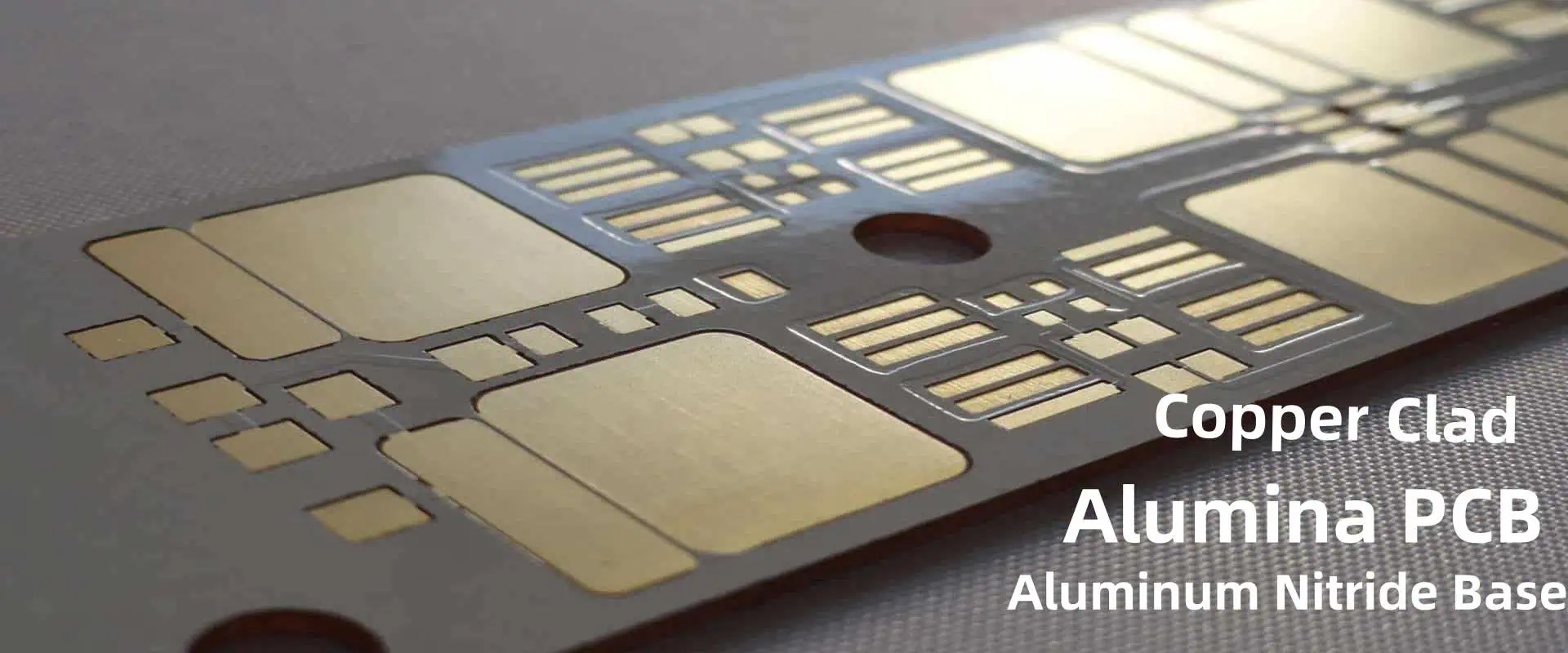
What is the difference between a flex circuit and a PCB?

quick turn flexible PCB prototype

Introduction

Printed circuit boards (PCBs) and flex circuits are common technologies used to interconnect electronic components and provide mechanical support. While both utilize conductive traces and pads on an insulating substrate, there are important differences between rigid PCBs and flexible circuits.

This article will examine the variations in materials, construction methods, performance capabilities, and typical applications for flex circuits versus PCBs. Understanding the tradeoffs involved can help designers select the optimal interconnection technology for each system.

PCB Overview

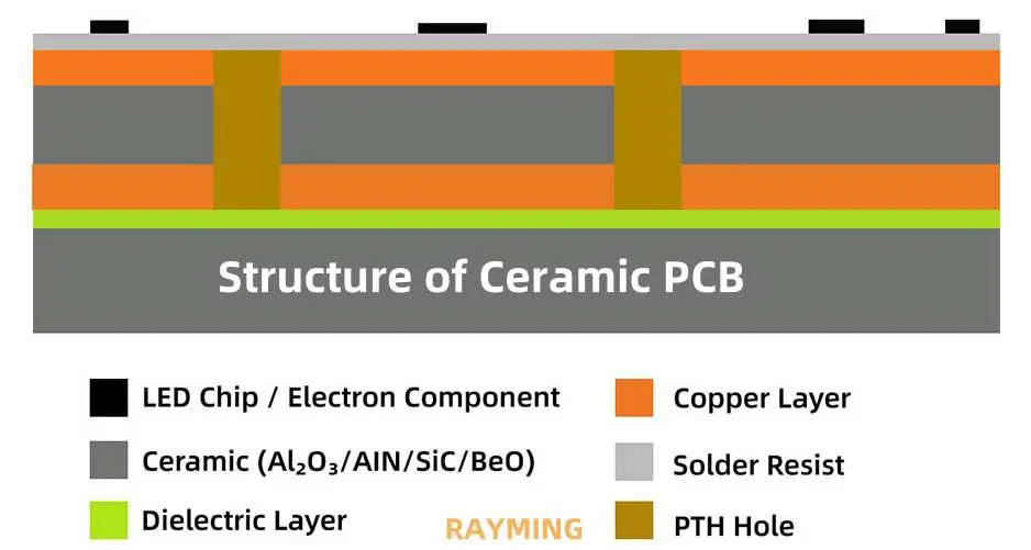
A printed circuit board consists of thin alternating layers of conductive copper and insulating dielectric substrate. The substrate material most commonly used is FR-4 fiberglass, which is rigid and relatively inexpensive. Other rigid laminate materials include FR-5, GETEK, and polyimide.

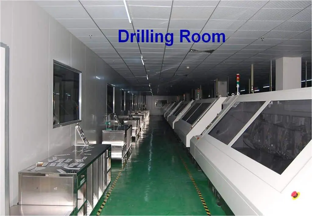
The board fabrication process generally includes:

  1. Drilling holes for component leads and vias
  2. Electroless copper plating to metallize the holes
  3. Laminating copper foil onto the substrate
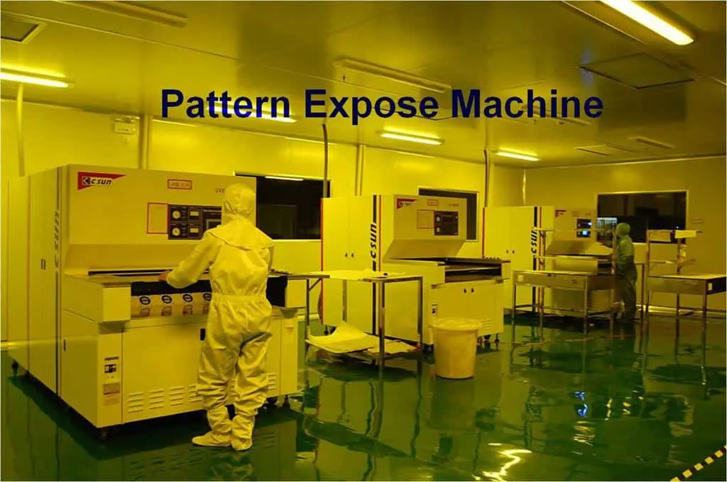
  4. Photolithography to print the circuit pattern onto the copper
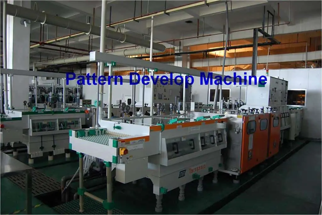
  5. Etching away unwanted copper to form isolated traces
  6. Applying protective solder mask over the traces
  7. Silkscreen printing of component designators

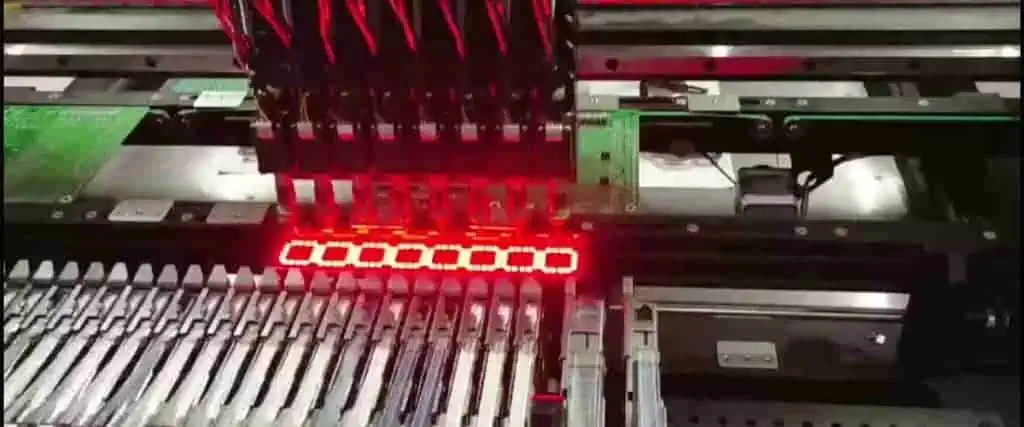
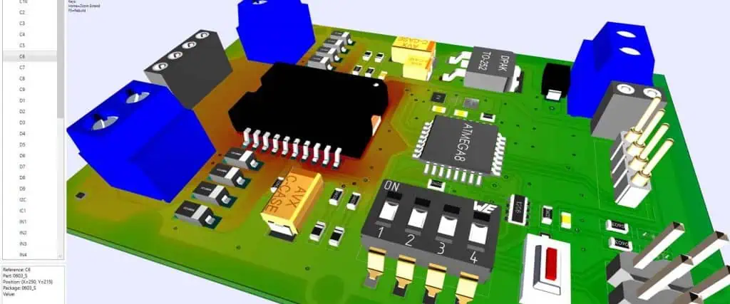
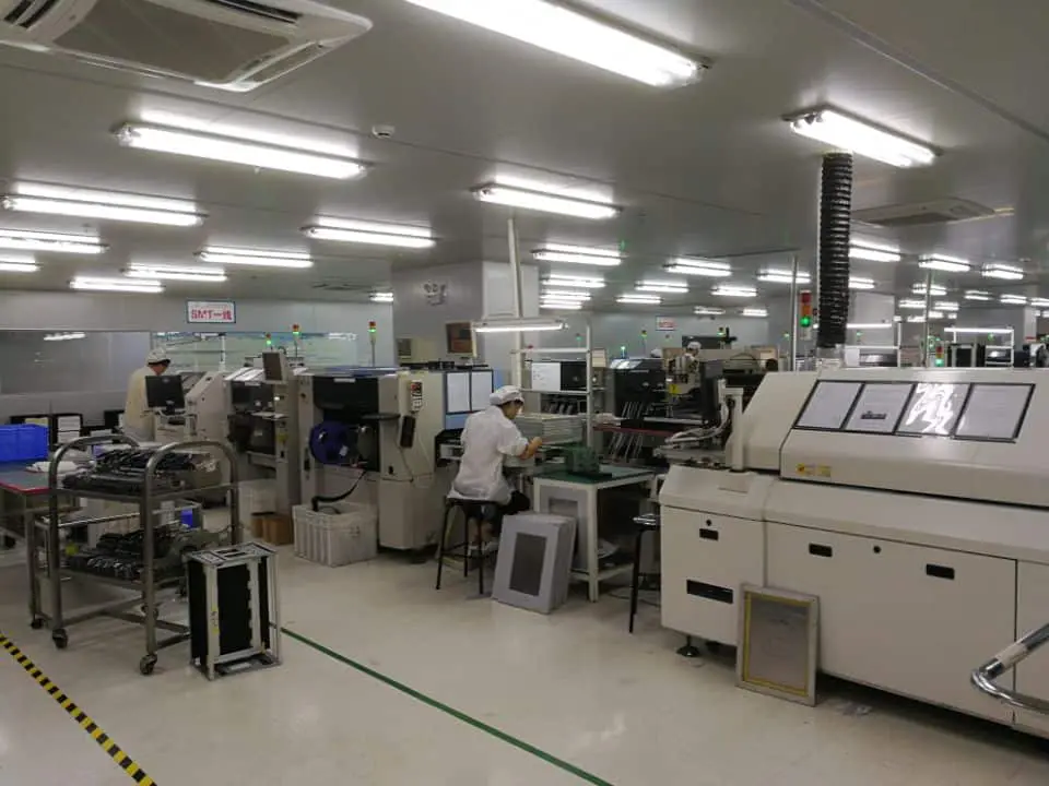
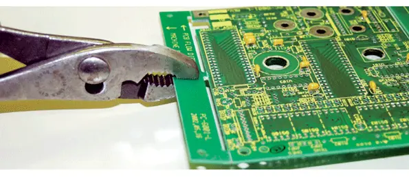
This subtractive process results in a rigid board with etched copper traces connecting surface mount and through-hole components soldered onto the pads. PCBs can be single, double, or multilayer with traces on both sides and internally between layers.

6 layer FR-4 PCB with surface mount and through-hole components

PCB Attributes:

  • Rigid fiberglass substrate
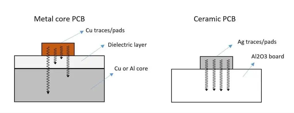
  • FR-4, FR-5, GETEK, polyimide, ceramic materials
  • Multilayer construction possible
  • High density interconnects
  • Fine line & space traces
  • Plated through hole vias
  • Lower cost process

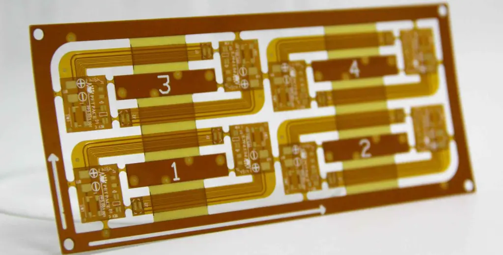
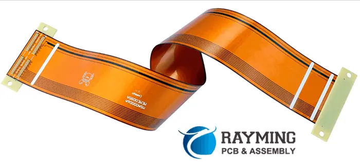
Flex Circuit Overview

YouTube video

A flex circuit consists of conductive traces and pads on a flexible dielectric substrate material. This allows the circuit to bend and flex dynamically during use. Polyimide films like Kapton or UPILEX are commonly used as the flexible insulating base material.

There are two main methods for creating a flex circuit:

Additive: An additive process is typically used for finer features. Conductive material is selectively deposited onto the substrate through masking and electroplating:

  1. A thin metal foil is laminated onto the substrate.
  2. Photoresist is applied and imaged to define the circuit pattern.
  3. Exposed areas are electroplated to build up the conductor thickness.
  4. Photoresist is stripped away, leaving the plated traces on an etched foil base.

Subtractive: A subtractive process can also create flex circuits, removing unwanted copper similarly to rigid PCB fabrication:

  1. An adhesive layer bonds a copper foil to the flexible substrate.
  2. Photoresist is laminated and imaged with the circuit layout.
  3. Exposed copper is chemically etched away.
  4. The remaining photoresist is stripped off.
flex-circuit-manufacturer

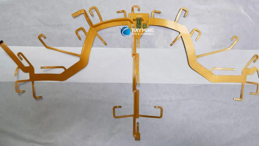
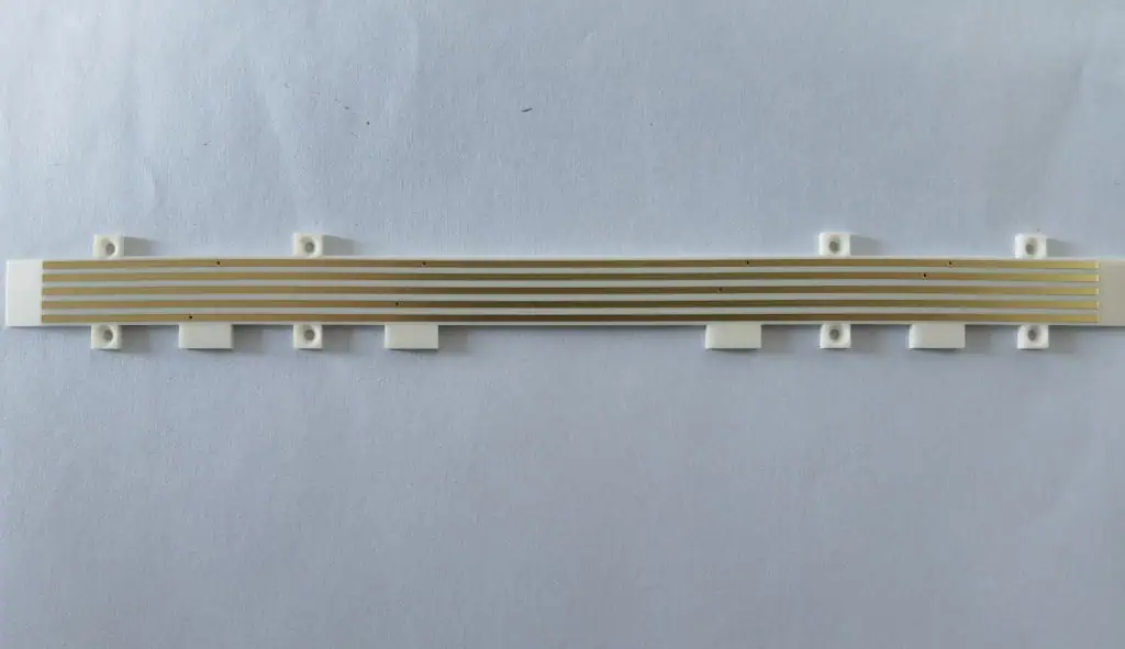
Polyimide flex circuit fabricated with an additive process

Flex Circuit Attributes:

  • Thin flexible substrate
  • Polyimide, PEEK, PET, TPU, PEN materials
  • Difficult to make multilayer
  • Tighter trace routing density
  • Finer lines and spaces
  • Flexible adhesive connections
  • Requires special handling

Physical Construction Comparison

PCBs and flex circuits vary quite a bit in terms of their physical construction and materials used:

ParameterPCBFlex Circuit
SubstrateFR-4, G10, GETEK, BTPolyimide, PEEK, PET
Dielectric Thickness1.6mm, 2.4mm typical25ฮผm – 75ฮผm typical
LayersUp to 30+ layersTypically single layer or double layer
Conductor1oz – 3oz copper foil0.5oz – 2oz rolled annealed copper
Line Width100ฮผm minimum15ฮผm possible
Line Spacing150ฮผm minimum25ฮผm minimum
Via ConstructionPlated through holeMicrovias, filled vias
FlexibilityRigidDynamic flexing capability
WeightHeavierLighter weight

Some key differences to note:

  • PCB substrates are thicker for structural rigidity, while flex circuits use thin flexible polymer films.
  • Multilayer constructions are common with PCBs but challenging with flex circuits.
  • Flex circuits can achieve finer trace widths and pitches.
  • Flex circuits are inherently flexible for dynamic movement requirements.

Performance Comparison

Flexible pcb board cost

The design objectives and use environment drives the performance requirements for an interconnection technology. Here is how PCBs and flex circuits compare for some key parameters:

Electrical Properties

MetricPCBFlex Circuit
Dielectric ConstantFR4: 4.5Polyimide: 3.5
Loss TangentFR4: 0.017Polyimide: 0.003
Insulation Resistance100 Tฮฉ typical20 Tฮฉ typical
Breakdown Voltage23 kV/mm16 kV/mm
Propagation SpeedFR4: 60%Polyimide: 85%
  • Flex circuits generally have lower loss and higher frequency performance.
  • PCBs can operate at higher voltages.
  • Match dielectric materials to application signal frequencies.

Mechanical Properties

MetricPCBFlex Circuit
Young’s ModulusFR4: 20-30 GPaPolyimide: 2.5 GPa
Tensile StrengthFR4: 275 MPaPolyimide: 231 MPa
Flexural RigidityVery low flexibilityCan bend dynamically
Thermal ExpansionFR4: 12-16 ppm/CPolyimide: 20 ppm/C
  • PCBs are rigid with high stiffness.
  • Flex circuits are flexible but have lower strength.
  • Coefficient of thermal expansion varies.

Environmental Resistance

MetricPCBFlex Circuit
Flammability RatingFR4: V-0Polyimide: V-0
Moisture AbsorptionFR4: 0.2%Polyimide: 2.0%
Chemical ResistanceFair acrylics, alcoholsGood overall
UV TolerancePoor – yellowsExcellent UV stability
Operational TemperatureFR4: 130ยฐCPolyimide: 260ยฐC
  • Both meet flammability standards for electronics.
  • Polyimide has broad chemical resistance.
  • Flex circuits withstand higher temperatures.

PCB vs. Flex Circuit Layout Comparison

The different construction and capabilities of PCBs and flex circuits require adapted layout strategies.

For PCBs, common practices include:

  • Partitioning circuits across multiple rigid layers
  • Escape routing component leads with clearance for etch and drilling
  • Area fills for power and ground planes
  • Grid-based placement with fixed 90ยฐ routing
  • High density surface mount components on both sides
  • Matching trace widths to current requirements
  • Impedance control traces and serpentine length matching

Flex circuit layout is characterized by:

  • Constrained to 1-2 flexible layers
  • Tight component placement and routing density
  • Curved traces following substrate contours
  • Selective reinforcements and stiffeners
  • Avoiding 90ยฐ traces and joints during flexing
  • Adhesive openings to isolate rigid sections
  • Careful management of cross-section changes
  • Fabrication-aware keepout margins

These examples illustrate the differing approaches needed to optimize layouts.

Typical Applications

Due to their distinct properties, PCBs and flex circuits tend to be used in very different types of products and assemblies.

Common PCB Applications:

  • Computer motherboards and expansion cards
  • Consumer electronics like phones and tablets
  • Telecommunications infrastructure equipment
  • Automotive engine control units (ECUs)
  • Industrial control systems
  • Power electronic converters
  • LED lighting drivers

PCBs provide an inexpensive rigid interconnection foundation for electronic subsystems and complex digital circuits. The modular nature allows assembly and servicing of individual boards.

Common Flex Circuit Applications:

  • Printers and scanners
  • Computer disk drives
  • Robotic arms
  • Medical imaging equipment
  • Fitness trackers and wearables
  • Avionics systems
  • Automotive sensors
  • High temperature electronics

When dynamic flexing, tight space constraints, or projected lifetime motion cycles are involved, flex circuits can provide reliable interconnects without wires or connectors. The continuous constructions allows flex circuits to fit product industrial design needs.

Cost Considerations

For low volume, PCBs generally have a lower cost per unit compared to flex circuits. The reasons include:

  • Economies of scale with massive worldwide PCB production volumes
  • Lower cost raw materials like standard FR-4
  • Highly automated fabrication processes
  • Mature assembly ecosystems and acceptance testing

As production quantities scale, flex circuits can reach similar price points for an overall system. Other considerations like these can also impact cost:

  • Layer count – Multilayer PCBs get exponentially more expensive
  • Fabrication yield – Thin flex circuits can have more waste
  • Connectors avoided – Flex circuits eliminate these costs
  • Testing – Both require verification time and overhead
  • Serviceability – Repairing flex circuits may require full replacement

The optimal choice involves weighing production volume, system complexity, product lifecycle, and manufacturing strategy tradeoffs.

Hybrid PCB/Flex Applications

In some cases, combining rigid PCBs with flex circuits provides an ideal solution. Some examples include:

  • Hinge connections: Flex circuits folding around a corner or hinge to interconnect PCBs. Used extensively in flip phones and laptops.
  • Screen connections: Flexible circuits connecting a display or touchscreen behind a device cover to the main PCB. Allows full range of adjustability.
  • Sensor arrays: Flex circuits create dynamic conformal sensor grids that attach to rigid sensor hub PCBs. Used in robotic skin, building HVAC monitors, and body networks.
  • Wearables: A rigid PCB provides processing and wireless functions, while flex circuits interconnect across clothing and accessories. Seen in rings, watches, and fitness bands.
  • Printers: Flex circuits span the moving print head assembly while connecting to controller boards. Also used in cameras and scanners.

For these applications, flex circuits essentially act as 3D interconnects integrated with planar PCBs when needed.

Summary and Recommendations

Here are some best practices based on the PCB and flex circuit comparison:

  • Select PCBs for static rigid boards with multilayer needs or high voltage.
  • Use flex circuits when flexibility, tight space, or motion cycling are critical.
  • Combine both technologies in a system when needed for modular and dynamic functions.
  • Match dielectric material properties to required performance characteristics.
  • Account for fabrication yield, testing, and serviceability costs.
  • Adapt layout and component selection to the properties of each technology.
  • Seek expert guidance to ensure a reliable design optimized for manufacturability.

Understanding these fundamental differences between printed circuit boards and flex circuits allows designers to make informed tradeoffs and utilize each technology appropriately.

FQA

What are the main differences between flex circuits and rigid PCBs?

The main differences are the flexible substrate material, thinner dielectric layers, finer traces, and dynamic flex capability of flex circuits versus the rigid multilayer FR4 construction and lower cost of traditional PCBs.

Why choose a flex circuit over a PCB?

Use flex circuits when the application requires tight space constraints, dynamic motion and flexing, or conformal shape adaptation that rigid boards cannot provide.

What are some examples of typical flex circuit applications?

Common uses include printers, disk drives, robotic joints, medical equipment, wearables, avionics, and automotive sensors. The flex circuits can adapt to motion and space requirements that PCBs cannot.

What are some typical applications for conventional PCBs?

PCBs are well suited for computers, servers, telecom systems, control systems, LED lighting, and consumer electronics where rigid support for multilayer digital circuits is acceptable.

When does using both PCBs and flex circuits together make sense?

PCB and flex circuit hybrid assemblies provide advantages in applications like laptops, wearables, printers, and sensors that have both dynamic flexible interconnections and rigid support or multilayer circuit needs.

What is the best waterproof coating for electronics?

PCB Assembly conformal coating

Introduction

Why should the PCBA brush conformal coating

Electronic devices and components exposed to moisture, humidity, condensation, or direct water contact are susceptible to corrosion, electrical leakage, and reliability failures. Protecting circuits and assemblies with waterproof coatings and encapsulants is critical for applications where electronics will encounter wet environments.

But with the wide variety of waterproofing materials available, how do engineers choose the optimal protective coating? Key factors to consider include the application requirements, coating properties, material compatibility, application methods, and qualification testing.

This article provides a detailed overview of waterproof coating technologies for electronics along with guidance on selection criteria and best practices. With an understanding of the different coating options and their capabilities, designers can make informed decisions on implementing the best waterproofing protection regimes for their products.

Waterproofing Requirements

The first step is identifying the specific waterproofing needs based on the application and operating environment:

  • Liquid exposure: Will the electronics encounter direct water submersion, pressurized sprays, splashing, or only incidental moisture?
  • Duration: Is water exposure occasional and temporary, or continuous for extended periods?
  • Chemical compatibility: Does the coating need to withstand specific fluids like saltwater, acids, or hydrocarbon oils?
  • Temperature range: What are the temperature limits for material performance?
  • UV and abrasion: Will the coating experience wear, UV radiation, or chemical degradation factors?
  • Repairability: Does the application require repairable/reworkable waterproofing?
  • Electrical properties: Are dielectric strength, surface insulation, and other electrical properties important?
  • Application method: Can the coating be cast, brushed, sprayed, or dip applied?

With an understanding of the environmental stresses and product requirements, the waterproof coating type can be selected.

Coating Properties

YouTube video

There are a wide variety of waterproof electronics coatings that seal components and PCB assemblies from moisture ingress and corrosion. Here are key performance properties to consider when comparing options:

Solvent and Curing

  • Solvent-cured: Use evaporation and chemical reaction of solvents to harden coating after application.
  • UV-cured: Cure rapidly upon exposure to UV irradiation. Minimal solvents.
  • Heat-cured: Apply as liquid or paste, then cure with oven baking process.
  • Room temperature cure: Cure at room temperature using catalytic chemical reactions.

Permeability

  • Impermeable: Cannot be penetrated by water molecules. Provides highest reliability.
  • Conformal: Thin coats follow PCB topology but allow slow moisture diffusion. Reliance on isolation layers.
  • Permeable: Absorbs moisture but provides temporary water resistance. Used with venting strategies.

Thermal and Mechanical

  • Operating temperature: Upper limit before coating degrades, typically 120ยฐC to 230ยฐC.
  • Coefficient of thermal expansion (CTE): Match to substrate to reduce stress and delamination.
  • Hardness and mar resistance: Resists abrasion, nicks, cuts. Shore D 65-85 typical range.
  • Adhesion: Bond strength to substrate, measured in psi. 500 psi minimum recommended.
  • Flexibility: Ability to bend without cracking. Important for flex PCB applications.

Electrical

  • Dielectric strength: Voltage withstand rating, reported in V/mil. 500-1500 V/mil target.
  • Dielectric constant: Impacts impedance and capacitance for coating thickness. 2.5-4.0 typical.
  • Insulation resistance: Resistivity in ฮฉ or Tฮฉ reflecting conduction losses.
  • Dissipation factor: Dielectric losses from polar molecules under AC excitation. Lower is better.

Material Types

Some of the main classes of waterproof electronics coatings include:

Acrylics

  • Simple, low cost resin coatings
  • Fast room temperature cure
  • Medium hardness and flexibility
  • Moderate temperature rating
  • Easy application by dip, spray, or brush

Urethanes

  • Tough, abrasion resistant coatings
  • Single or two part chemistries
  • Temperature, UV, and chemical resistant
  • Excellent adhesion and flexibility
  • Can be rigid or rubber-like

Silicones

  • Inorganic silicone polymers
  • Very broad operating temperature range
  • Excellent moisture and UV resistance
  • Conformal thin film coats with high elasticity
  • Moderate dielectric strength

Epoxies

  • Strong adhesion and environmental resistance
  • Range of flexible to rigid coatings
  • Excellent dielectric properties
  • Withstand rugged use conditions
  • Room temperature or heat cure options

Parylenes

  • Unique vapor deposited polymer films
  • Extremely conformal thin coats
  • Superb dielectric strength and moisture barrier
  • Expensive process with high capital costs

This covers some of the major coating material types. Comparing options within each category based on specific needs is key.

Waterproof Coating Methods

PCBA Conformal Coating

There are several approaches to protect electronics from water exposure:

Conformal Coatings

Conformal coatings provide thin layers that follow the contours of components and PCBs. Common coating methods include:

  • Spray: Automated selective spray systems or manual aerosol cans deposit controlled coats.
  • Brush: Manual application allows selective brushing but can leave voids.
  • Dip: Full immersion followed by controlled withdrawal leaves a thin uniform coat.
  • Vapor deposition: Parylene coatings are applied as gaseous monomers that polymerize onto surfaces.

Typical conformal coat thickness ranges from 25-75 ฮผm. While offering some water resistance, conformal coats rely on the PCB soldermask layer as the primary water barrier.

Conformal epoxy coating applied over PCB assembly

Potting Compounds

Potting fills the entire electronics enclosure with a thick protective resin encapsulant:

  • Casting: Liquid resins poured or injected then cured to harden
  • Compression: Potting compounds compressed around components
  • Impregnation: Vacuum draws resin into complex assemblies

Typical potting thickness from 2mm up to 25mm. Provides excellent water resistance but limits access for rework.

Electronic device encapsulated with thick potting material

Sealed Housing

For the most critical applications, electronics can be entirely sealed within a watertight enclosure:

  • Plastic or metallic housings: O-ring or gasket sealed, often with added potting material
  • Hermetic housings: Use welded or soldered metal enclosure with added desiccant to maintain <1% internal humidity

This provides protection for continual or extreme submersion but with higher cost. Regular seal inspection and maintenance may be required. Accessing internals becomes difficult.

Electronics assembly sealed within a hermetic metal enclosure

Selection Criteria

PCB-circuit-board-waterproof-coating

Choosing an optimal waterproofing approach requires tradeoffs across many factors:

Exposure Level

  • For temporary moisture or rain exposure, conformal coating provides adequate protection.
  • Applications with prolonged submersion will require potting material or a fully sealed housing.

Mechanical Properties

  • Conformal coats maintain flexibility for dynamic components and flex PCBs.
  • Brittle potting compounds require fixed rigid support.

Thermal Properties

  • Conformal coats allow convection and air cooling of electronics.
  • Thick potting compounds act as a thermal insulator requiring other cooling methods.

Electrical Performance

  • Conformal coats have limited dielectric strength and higher capacitance.
  • Potting better withstands voltage exposures but may require insulation displacement.

Repairability

  • Conformal coats can be selectively reapplied after rework.
  • Encapsulants prevent access to components without full removal.

Weight

  • Thin conformal coats minimize weight impact.
  • Dense potting resins increase weight, which may be prohibitive.

Cost

  • Adding conformal coat has lower material cost but process impact.
  • Potting resins and sealed housings have higher material expense.

With an understanding of these considerations against application requirements, the optimal coating method can be selected.

Qualification Testing

Verifying a chosen waterproof coating will meet product reliability requirements under real-world conditions is critical. Typical qualification tests include:

Coating Cure Validation

  • Measure shore hardness to confirm full cure
  • Exposure to excess working time to check for tackiness or soft spots
  • Thermal shock or rapid temperature ramping
  • Sample cross-sectioning to validate uniform cure

Adhesion Testing

  • ASTM D3359 crosshatch tape tests
  • Initial adhesion and after thermal cycling
  • Pull-off adhesion tests before and after liquid exposure

Electrical Properties

  • Dielectric breakdown voltage
  • Insulation resistance
  • Combing resistance under bias voltage
  • Capacitance changes from coating

Fluid Exposure

  • Salt spray fog per ASTM B117 standard
  • Thermal shock and moisture cycling
  • Water submersion and chemical compatibility
  • Flammability testing after exposure

The specific test conditions and performance requirements will depend on the product specifications and reliability models. But following a thorough qualification protocol matched to application conditions ensures the coating will function as needed.

Application Best Practices

Conformal Coating
Conformal Coating

Properly applying waterproof electronics coatings is vital for achieving protection. Key guidelines include:

Surface Preparation

  • Ensure PCBs are clean and dry before coating
  • Remove contaminants like rosin residue
  • Lightly abrade glossy soldermask
  • Apply adhesion promoter if needed

Process Controls

  • Maintain ambient conditions like temperature and humidity
  • Use clean tools dedicated for coating
  • Have proper PPE and ventilation
  • Carefully measure mixing ratios for multi-part coats

Coverage Assurance

  • Mask connectors or test points to avoid coating
  • Ensure full coverage on all components and PCB edges
  • Apply multiple coats for thick buildup if needed

Curing

  • Gradually ramp oven temperature for heat cure coatings
  • For UV cures, match wavelength to coating reaction
  • Validate full cure with testing before proceeding

Coating Repair

  • Spot repair thin coats rather than full removal
  • Have contingency plan for thicker encapsulant removal
  • Plan accessibility provisions into design

Adhering to structured processes ensures the chosen coating consistently provides reliable waterproofing protection.

Summary

Protecting electronic products from water exposure threats requires selecting the optimal protective coating for the specific application conditions and requirements. Key takeaways include:

  • Carefully consider liquid exposure levels, coatings properties, material compatibility, reparability needs, and other criteria.
  • Determine if thin conformal coating, thick potting encapsulant, or sealed housing provides the right level of protection.
  • Match candidate coatings to physical, electrical, and environmental reliability requirements.
  • Qualify top coating options with standards-based testing tailored to end use stresses.
  • Follow robust process controls and best practices during coating application.

By understanding the wide range of waterproofing options and how to select the best fit, engineers can implement effective water protection regimes for electronics operating in wet environments.

FQA

What are some typical applications requiring waterproof coatings on electronics?

Typical applications are outdoor equipment, marine electronics, automotive systems, appliances, IoT sensors, medical devices, industrial controls in washdown environments, and consumer electronics where liquid resistance is valued.

When is it preferable to use a thick potting encapsulant versus a thin conformal coating?

Potting makes sense for full submersion applications where conformal coats would allow moisture diffusion over time. Use thin coats when flexibility, repairability, weight impact, or thermal dissipation are critical.

What electrical factors should be considered when selecting a waterproof coating?

Key electrical factors are dielectric breakdown voltage rating, insulation resistance, dielectric constant, dissipation factor, and surface resistivity. Match coating properties to PCB layout clearances and any high voltage exposures.

How is a waterproof coating qualified for use in a particular product?

Typical qualification steps are evaluating coating cure consistency, verifying adhesion strength before and after reliability testing, measuring electrical properties, and exposing samples to simulated end use environments like salt fog or liquid submersion.

What are some best practice guidelines for applying waterproof electronics coatings reliably?

Best practices include proper surface preparation, process controls on ambient conditions and mixing, full coverage verification, controlled ramps for heat cures, validating full cure prior to further assembly, and having repair contingencies planned for.

What are the common problems with PCB and PCBA?

PCB soldering problems

Introduction

Printed circuit boards (PCBs) and printed circuit board assemblies (PCBAs) are at the heart of electronics, providing the platform to mount and interconnect components. However, many potential defects can occur with PCB fabrication and PCBA assembly if processes are not optimized and controlled.

This article examines the most frequent problems that arise with PCBs and PCBA production, including root causes and steps to detect and prevent issues from impacting quality and reliability. Understanding common failure modes enables proactive process improvements.

PCB Fabrication Defects

Best way to solve the PCBA process problems

PCB fabrication involves many steps including design, materials processing, photolithography, plating, etching, lamination, drilling, routing, finishing, and testing. Errors can be introduced at any stage:

Design Errors

  • Netlist mismatches
  • Undefined pin-pairs
  • Incorrect stackup configuration
  • Excessive unrouted nets
  • Violating design rules

Thorough design rule checking and manufacturing reviews of the layout and documentation prevents converting flawed designs into PCBs.

Material Defects

  • Glass weave fuzz balls
  • Resin voids
  • Copper nodules
  • Contamination from fiberglass strands

Incoming materials inspection and statistical process control tracking can isolate problematic materials batches.

Registration Errors

  • Layer-to-layer misalignment
  • Soldermask to pad misregistration
  • Silkscreen legend shifting

Fiducial mark inspection and optical registration measurement validates alignment at each process stage.

Etching Defects

  • Undercut traces from over-etching
  • Copper thinning from over-exposure
  • Open circuits from splashes and pitting
  • Partial copper due to mask damage

Optical inspection and test coupon characterization provide etch process control.

Plating Flaws

  • Insufficient hole wall copper
  • Voids within plated layers
  • Unfilled internal plane connect holes
  • Nodules or dendrites in plating tanks

Coupon analysis and test panel examination give plating process feedback.

Drilling Issues

  • Hole tolerance deviations
  • Burrs, nicks, and rough walls
  • Smear shorting holes to pads
  • Drill breakage damaging layers

Automated optical inspection (AOI) and hole wall microscopy checks ensure drill quality.

Lamination Problems

  • Resin starvation around heavy copper
  • Bowed or twisted boards
  • Delamination and blistering
  • Prepreg voids

Microsectioning and x-ray imaging validates lamination quality.

PCBA Assembly Defects

Populating a PCB involves soldering, adhesive application, cleaning, inspection, and testing steps. Many potential assembly process flaws can affect PCBA quality:

Soldering Defects

  • Insufficient or excess solder
  • Solder balls/spikes
  • Solder bridging
  • Cold/disturbed joints
  • Pad lifting or tombstoning
  • Component miss-orientation
  • Incorrect or missing parts

Automated optical inspection (AOI) of every board validates assembly integrity against the bill of materials (BOM) and component placement (XYR).

Adhesive Flaws

  • Insufficient adhesive
  • Overflow or icicles
  • Component tilt or slide
  • Voids under components
  • Cracked or brittle adhesive

Process monitoring and inspection verifies proper adhesive dispensing, coverage, and curing.

Cleaning Issues

  • Residual flux or splatter
  • Pad corrosion from cleaning solutions
  • Component damage from harsh chemicals
  • Moisture ingress without drying

Cleanliness testing by ionic contamination measurement ensures post-solder residues are sufficiently removed.

Board Damage

  • Pad lifting during depanelization
  • Flex cracks from handling
  • Scratched traces or solder mask
  • Broken components or leads

Proper depanelization fixture design and operator training protects board integrity through assembly steps.

Application Errors

  • Miscalibrated sensors
  • Software bugs
  • Incorrect component values
  • Faulty circuit designs

Thorough electrical testing under operational profiles and environmental stress screening verifies proper PCBA functionality.

Root Cause Analysis

pcb Failure Analysis

When defects occur, structured root cause analysis is key to identify corrective actions:

  • Review all process data for abnormalities around the failure timeframe.
  • Characterize the defect morphology and mechanism.
  • Correlate observations to process interactions that could induce the defect.
  • Identify potential capability gaps or variability risks.
  • Determine if process adjustments, training improvements, or other interventions could reduce the specific defect mode likelihood going forward.

Effective root cause analysis drives process maturity while optimizing quality and reliability.

Mitigation Strategies

Here are approaches to detect and minimize some of the most common PCB and PCBA defect types:

Design Validation

  • Formal design reviews against fabrication capabilities and assembly requirements.
  • Testability analysis for access and diagnostics.
  • Design rule checking automation.
  • Prototype test runs to validate performance.

Incoming Material Controls

  • Material certification requirements for suppliers
  • Sampling and testing procedures
  • Process monitoring for storage conditions
  • Statistical tracking of defect rates

Process Control Standards

  • Define process requirements and tolerances
  • Create control plans for critical parameters
  • Validate capabilities and stability
  • Employ mistake-proofing systems
  • Automate process data logging

Inspection and Testing

  • Optical automated inspection of PCBs and PCBA
  • Ionic contamination testing for cleanliness
  • Functional testing of every board
  • Burn-in stress testing on samples
  • Failure analysis when defects occur

Training and Documentation

  • Certification training for inspectors and operators
  • Visual work instructions for each process
  • Flowcharts and control plan documentation
  • Change management procedures

Continuous Improvement Culture

  • Root cause analysis for defects
  • Lean manufacturing principles
  • Idea solicitation system
  • Standardized corrective actions
  • Process audits

This framework of aligned quality practices minimizes common PCB and PCBA defects to maximize manufacturing yields.

Defect Prevention Guidelines

Soldering Defects

Here are some key guidelines for avoiding frequent PCB and PCBA problems:

  • Start with design validation – Don’t build in quality risks
  • Validate incoming materials – Avoid latent defects
  • Measure process capability and stability – Know your limits
  • Inspect end product quality – Detect issues early
  • Perform electrical testing – Ensure functionality
  • Monitor defect rates – Identify negative trends
  • Do root cause analysis – Address systemic gaps
  • Standardize processes – Reduce variability
  • Automate when possible – Take human error out
  • Implement controls and mistake-proofing – Make it foolproof
  • Certify and train everyone – Build in quality at each step

Building a culture focused on defect prevention brings tremendous quality and cost advantages.

Conclusion

Avoiding common PCB and PCBA defects requires knowledge of potential failure modes, rigorous process control standards, extensive inspection regimes, robust corrective systems, and a commitment to continuous defect reduction.

By leveraging quality management discipline along with statistical process monitoring, automated inspection, mistake-proofing devices, and other best practices, organizations can maximize yields. This reduces costs while ensuring customers receive reliable electronic hardware.

Understanding the most frequent problems, their root causes, and effective mitigation strategies empowers teams to avoid PCB and PCBA defects proactively. That knowledge helps electrical engineers work closely with fabrication and assembly partners to prevent quality issues and implement impactful process improvements.

FQA

What are some typical PCB fabrication defects and their causes?

Common PCB defects include opens/shorts from etch issues, registration errors like layer shifts, plating voids, material impurities, drill smearing, and others caused by process variability and capabilities.

What are common PCBA assembly defects?

Typical PCBA defects are soldering flaws like shorts, voids, bridging and tombstoning, improper component placement, board damage, adhesive issues, inadequate cleaning, and functional failures from design or component problems.

How can organizations avoid common PCB and PCBA defects?

Strategies include design validation, material qualification, process control standards, automated inspection, functional testing, continuous improvement culture, worker training, and root cause analysis to address systemic weaknesses.

What are some key process control and monitoring methods to reduce defects?

Critical process controls include defined requirements, stability monitoring, Statistical Process Control (SPC), capability validation, mistake-proofing, standardized work, inspection, corrective systems, audits, and a focus on continuous defect reduction.

Why is root cause analysis important for PCB and PCBA defects?

Root cause analysis identifies systemic process gaps or weaknesses so that permanent corrective actions can be implemented, reducing future defect likelihood and preventing wasted effort on temporary containment fixes.

How much does it cost to assemble a PCB?

PCB Assembly Introduction

Introduction

The assembly of printed circuit board assemblies (PCBA) involves significant labor, equipment, and overhead expenses for contract manufacturers (CMs). While the exact PCBA assembly cost depends on many factors, understanding what drives pricing can help product developers budget and source assembly services strategically.

This article examines PCBA assembly cost drivers including materials, processes, testing, quality factors, location, production volumes, and complexity. Weโ€™ll look at how pricing varies based on these attributes and discuss cost optimization tactics. With insight into PCBA assembly economics, engineers can estimate and manage assembly costs effectively.

Cost Overview

The core expenses making up PCBA assembly pricing consist of:

Materials โ€“ Components, solder, adhesives, PCBs

Direct labor โ€“ Operators running production and testing

Equipment โ€“ Soldering, dispensing, cleaning, test systems

Facility costs โ€“ Space, utilities, depreciation

Overhead โ€“ Management, quality, logistics, IT, etc.

Margin โ€“ CM profit margin expectation

There are many variables determining the specific price for a given PCBA product based on how these elements scale.

Letโ€™s examine some of the key factors influencing cost in detail…

Materials Cost

Component costs often dominate the total PCBA material expenses:

  • Active ICs – Microcontrollers, power semiconductors, FPGAs
  • Passives – Resistors, capacitors, inductors, transformers
  • Connectors, cables, hardware
  • Mechanical parts like housings or fasteners

The bill of materials (BOM) largely defines the base material cost. Component pricing depends on:

  • Component type – ICs cost more than simple resistors
  • Package style โ€“ Surface mount is less costly than through-hole parts
  • Lead count โ€“ More leads or terminations add cost
  • tolerances โ€“ Tighter specs increase price
  • Quantity โ€“ High volumes command discounts
  • Lifecycle โ€“ Late life components can have inflated pricing

Beyond components, other materials like solder paste, adhesives, labels, and hardware add cost.

Labor Cost

The complexity of the assembly process and test requirements determines labor utilization:

  • Loading PCBs into equipment
  • Solder paste dispensing
  • Robotic and manual component placement
  • Soldering – Reflow oven, wave, selective systems
  • Adhesive and encapsulant dispensing
  • Conformal coating or potting steps
  • Cleaning assembled boards
  • Testing – In-circuit, functional, burn-in, optical inspection
  • Kitting, packing and shipping

High labor content processes like selective soldering or complex testing add cost. Automation offsets labor for repetitive tasks.

Factory Overhead

Running an EMS factory involves considerable overhead expense:

  • Facility costs – Building, utilities, property tax, insurance
  • Management and admin salaries
  • Quality and engineering staff
  • IT infrastructure and software
  • Equipment maintenance and facilities upkeep
  • Training and compliance
  • Supply chain, planning, finance departments

These relatively fixed costs are spread across production volumes making overhead significant at low volumes.

Equipment Utilization

Specialized production and test systems required for PCBA processes impact equipment cost:

  • Soldering – Reflow ovens, selective systems, wave solder
  • Dispensing – Solder paste printers, adhesive dispensers
  • Testing – Flying probe, boundary scan, functional testers
  • Software – CAD, CAM, MES, ERP, quality systems
  • Handling – Conveyors, hoists, racks, static control
  • Cleaning – Aqueous washers

Capital equipment depreciation and maintenance is incorporated into unit pricing. Newer systems may enable higher throughput to offset cost.

Location Factors

Where assembly is performed greatly impacts costs:

Low cost regions:

  • China – Extensive supply chain infrastructure and competition
  • Southeast Asia – Malaysia, Vietnam – Lower wages than China
  • Mexico – Reduced shipping and logistics to North America

Higher cost regions:

  • United States & Canada – Limited low cost providers
  • Western Europe – Higher wages, overhead, regulations

Labor, facilities, and materials costs vary based on country and region. Shipping also factors in.

Quality

The cost of quality depends on:

  • Yield – Scrap and rework reduce margins
  • Process control – Manual processes generate more defects
  • Inspection – Automated optimal vs manual visual
  • Testing – High coverage vs simple spot checks
  • Documentation – Detailed reporting increases overhead
  • Corrective action – Preventing defects has lower cost than containment
  • Qualification – Certification audit expenses

Quality programs to maximize PCBA yields and reliability have associated costs but pay dividends long-term.

Volume Effects

pick and place machine for pcb assembly

PCBA pricing is extremely dependent on production volumes:

VolumePricing Factors
PrototypesVery high touch labor, small batches, expedited materials
Low VolumeManual processes, changeovers, smaller batches
Medium VolumeTransition to automation, improved scheduling
High VolumeHighest automation, process optimization

Economies of scale substantially reduce cost per unit at volume. Fixed overhead is distributed across more boards.

Design Complexity

A PCBAโ€™s physical design attributes impact assembly labor and materials complexity:

  • Component types – Lots of connectors or odd parts
  • Component sizes – Many tiny passives require inspection
  • PCB technology – Multilayer vs simple double sided board
  • Board shape and size – Rectangular boards allow panelization
  • Component placement – Both sides vs single side placement
  • Component count – More components takes more operator time
  • Density – Fine pitch and spacing need special tooling
  • Routability – Completely routed vs wire jumps
  • Solder points – DFNs, BGAs, QFNs require process care
  • Selective coatings – Extra steps for solder masks or potting

Complexity factors result in more production and inspection steps and drive cost.

NRE and Tooling

Upfront non-recurring engineering (NRE) and tooling costs include:

  • Design review
  • Test development
  • Programming placement and inspection routines
  • Solder masks and stencils
  • Handling fixtures
  • Any long lead tooling

These one-time expenses are allocated into unit pricing depending on volumes. For short run prototypes, NRE costs can dominate pricing.

Geography

Shipping assembled boards long distances adds cost:

  • Air freight has high cost for any volume
  • Sea shipping has low cost per unit but long transit time
  • Customs, duties, and taxes may apply

Manufacturers strategically locate facilities to optimize logistics costs.

Vertical Integration

Some contract manufacturers offer services throughout the product life cycle:

  • Design – Full development capabilities including PCB layout
  • Prototypes – Low volume assembly with quick turnarounds
  • Volume production – Scalability to high volumes with global facilities
  • Testing – Extensive test development and coverage
  • Box build – Subsystem and full product assembly
  • Distribution – Custom packaging, kitting, logistics
  • Lifecycle management – Aftermarket support, repair,Upgrades
  • Software, firmware, FPGA development

Leveraging vertically integrated partners reduces interface complexity but can command pricing premiums.

Cost Optimization

Here are tips to optimize PCBA cost:

  • Standardize: Use common components in consistent packages, reduce custom connectors, minimize board sizes and layer counts.
  • Design for Mfg: Enable automated assembly and test. Eliminate placements requiring manual steps.
  • Evaluate global supply: Consider qualified offshore sources to realize labor, overhead, and regional supply chain benefits.
  • Review BOM pricing: Check alternate suppliers and lifecycle status for inflated components. Standardize vendors.
  • Leverage volumes: Commit to forecasted volumes and contract terms to earn scale benefits. Consolidate multiple boards into fewer part numbers.
  • Relationships and partnerships: Develop transparent win-win relationships with CMs leveraging their expertise.

Keeping these key cost drivers in mind while making design and sourcing decisions helps manage PCBA assembly pricing.

Cost Estimation Guidelines

While the complexity of cost estimation varies based on product specifics, this provides a general calculation sequence:

  1. BOM pricing – Use manufacturer published price lists for the exact quantities needed of each component.
  2. NRE expenses – Estimate or obtain quote for any upfront NRE, tooling, test equipment, etc.
  3. Material overhead – Add overhead markup percentage to direct BOM cost to cover material handling, inventory, qualification etc. (e.g. 10-15%)
  4. Unit labor cost – Work with CM to estimate touch labor time for each assembly and test process based on complexity factors. Multiply by shop floor hourly rate.
  5. Equipment utilization – Estimate production equipment runtime for the process steps and factor in hourly cost rates.
  6. Factory overhead – Apply factory indirect labor, facilities, utilities, and services overhead rate to direct hours. (e.g. 2-4X direct labor)
  7. Quality and yield – Add cost impact of any sampling, inspection, containment, rework, scrap etc. based on historical norms.
  8. Logistics – Local vs international shipping and customs costs.
  9. Margin – Apply typical margin targets based on volumes and competitiveness. (e.g. 15-30+%)

While simplified, this model allows a realistic budgetary estimate and reveals where opportunities exist to refine manufacturing and design strategies.

Summary

through-hole assembly process

Estimating and minimizing PCBA assembly costs requires understanding key drivers:

  • Materials – Component types, packaging, volumes
  • Labor – Manual steps, complexity factors
  • Overhead – Quality, infrastructure, services
  • Equipment – Automation offsets capital costs
  • Location – Labor rates, logistics
  • Volumes – Higher utilization and scale efficiencies
  • Design – Standardization, DFM, testability

Armed with knowledge of cost factors, engineers can make informed design tradeoffs and sourcing selections to achieve cost-optimized PCBA production.

FQA

What are the main elements making up overall PCBA assembly cost?

The primary PCBA assembly costs consist of materials (components, PCBs, consumables), direct labor, equipment depreciation, factory overhead, quality programs, logistics, NRE expenses, and manufacturer profit margin.

What design factors typically increase PCBA assembly cost?

Design choices increasing cost include high component counts, small passives, dense BGAs/QFNs, multiple layers, routing complexity, selective coatings, large board sizes, and designs needing manual steps or exotic tooling.

How does production volume impact PCBA assembly pricing?

Low volumes have very high cost due to setup, tooling, manual processes. Costs decline sharply as volume increases thanks to automation, process optimization, and overhead absorption.

What is the most significant variable determining assembly location economics?

The predominant factor driving regional assembly pricing is local labor rates, which imposes a large variable cost component. Other factors include supply chain infrastructure, logistics, and facility costs.

What are effective ways engineers can design PCBA to optimize manufacturing cost?

Optimizing assembly cost involves standardizing components, reducing lead counts, enabling SMT over through-hole parts, minimizing layers and board sizes, and designing for automated assembly and testability.

PCB Thermal Conductivity Performance: FR4 Vs. Ceramic Vs. Metal Core Vs. Rogers

Introduction

Managing heat dissipation is critical for reliable and efficient PCB design. The choice of printed circuit board substrate material has a major impact on thermal performance. Materials like FR4, ceramic, metal core PCBs, and Rogers laminates each provide different thermal conductivity properties.

This article compares the thermal characteristics of common PCB substrate types. Weโ€™ll examine the composition, thermal conductivity, dielectric properties, design considerations, and typical applications for each material class. With an understanding of material thermal capabilities, PCB designers can select the optimal approach for their thermal management needs.

Thermal Conductivity Basics

Ceramic PCB Thermal Conductivity

Thermal conductivity indicates how effectively a material transports heat. It is defined as:

K = Q x L / A x ฮ”T

Where:

K = Thermal conductivity in W/m-K

Q = Heat flow rate in Watts

L = Material thickness in meters

A = Material cross sectional area in m^2

ฮ”T = Temperature difference across material in Kelvin

Materials with higher thermal conductivity (K) values conduct heat more efficiently across a temperature gradient.

For PCBs, thermal conductivity directly impacts how much heat from components and traces flows into the board substrate, as well as spreading across the substrate internally. This heat must ultimately be dissipated to avoid temperature buildup.

FR4 Thermal Performance

fr4 thermal conductivity

FR4 glass reinforced epoxy is the most common and cost effective rigid PCB substrate. However, it suffers from poor thermal conductivity:

Composition

FR4 consists of layers of fiberglass fabric reinforcements impregnated with an epoxy resin binder. The glass fibers provide mechanical rigidity while epoxy gives adhesion and environmental resistance.

Typical multilayer FR4 PCB construction

The glass content typically ranges from 30% to 70% by weight depending on thickness. Higher fiber content increases thermal conductivity but reduces dielectric strength.

Thermal Conductivity

The thermal conductivity of FR4 is highly anisotropic due to the woven fiberglass layers:

  • In-plane (X-Y direction) = 0.25 – 0.30 W/m-K
  • Through-plane (Z direction) = 0.10 – 0.20 W/m-K

The in-plane conductivity is 2-3X higher than through thickness. But even in-plane, FR4 is a very poor conductor compared to metals or ceramics.

Design and Performance Challenges

The limited through-plane conduction hinders heat spreading from hot components into the board:

FR4 exhibits poor thermal spreading from localized heat sources

High power components can experience considerable temperature rise with FR4, risking reduced reliability and performance. Adding thermal vias helps somewhat but is limited by low through-thickness conductivity.

Typical FR4 Applications

Despite thermal constraints, FR4 excels in many applications:

  • Consumer electronics
  • Computers and peripherals
  • Automotive electronics
  • Cost-driven designs
  • Moderate temperature environments

FR4 provides the most affordable PCB substrate for many commercial and industrial products not needing advanced thermal performance.

Ceramic PCB Thermal Performance

Ceramic printed circuit boards provide an order of magnitude better thermal conductivity than FR4, though at higher cost:

Composition

Ceramic PCB substrates consist of aluminum oxide (alumina) or aluminum nitride ceramic filler particles combined with a glassy binding matrix. This produces a crystalline ceramic material.

Common material grades include:

  • Alumina (Al2O3) – 92% to 99% purity
  • Aluminum nitride (AlN) โ€“ Over 90% purity

A metal layer (copper, aluminum) typically clads the ceramic base to enable circuit patterning.

Aluminum nitride ceramic PCB

Thermal Conductivity

The thermal conductivity of ceramic PCB materials far surpasses traditional FR4:

  • Alumina: 24 – 30 W/m-K
  • Aluminum nitride: 170 – 250 W/m-K

This enables efficient lateral and vertical heat spreading. The high purity minimizes defects that would impede heat transfer.

Design and Performance

The excellent thermal conduction allows heat to spread across a larger board area:

Aluminum nitride ceramic exhibits superior thermal spreading

Ceramic PCBs can dissipate very high component heat fluxes while maintaining lower temperatures. The rigid structure also resists warping.

Typical Ceramic PCB Applications

The cost of ceramic material relegates usage to high performance and reliability applications:

  • High power electric vehicle inverters and charging
  • Power supply converters
  • Industrial power and control
  • RF and microwave boards
  • Hybrid microelectronics
  • Aerospace and defense electronics

Ceramic PCBs support the demands of power electronics and microwave circuits where thermal and dielectric performance are critical.

Metal Core PCB Thermal Performance

Metal core PCBs utilize a thick metal base layer to maximize heat spreading and thermal mass:

Composition

Metal core PCBs contain a 0.8mm to several mm thick aluminum or copper layer at the core. Dielectric material layers bond circuit layers to the metal foundation.

Typical metal core PCB construction

Common dielectric layers include polyimide films, epoxy composites, and ceramic substrates. Direct Bonded Copper (DBC) integrates a ceramic layer.

Thermal Conductivity

The metal base provides exceptional thermal conduction:

  • Aluminum: 150 – 230 W/m-K
  • Copper: 400 W/m-K

This enables large heat quantities to be absorbed and spread over the entire board. The thermal mass also promotes lateral conduction.

Design and Performance

Metal core PCBs manage the most extreme thermal loads:

Metal core heat spreading and sinking

The thick metal base acts as both a heat spreader and heatsink, ideal for high power densities. Heat can also be removed via the backside.

Typical Metal Core PCB Applications

The cost and specialized fabrication restricts metal core PCBs to very high power products:

  • Power converters and inverters
  • Motor drives
  • Power amplifiers
  • High brightness LED lighting
  • Wind and solar power electronics
  • Electric vehicle drives

If thermal performance is the paramount priority, metal core PCBs conduct heat extremely efficiently.

Rogers Laminates Thermal Performance

PCB thermal resistance

Rogers Corporation (Chandler, AZ) produces premium PCB substrate materials focused on high frequency applications. Many of Rogersโ€™ circuit materials also offer improved thermal conductivity over FR4 while being cost-effective for high volume commercial products:

Composition

Rogersโ€™ materials utilize fluoropolymer resin systems reinforced with glass fabric. Some products incorporate ceramic filler particles to enhance thermal performance.

Typical Rogers laminate PCB construction

Popular materials include RO4350, RO4003, RT/duroid 6202, and LoPro series laminates. They exhibit a good balance of electrical and thermal properties not found in FR4.

Thermal Conductivity

Rogersโ€™ circuit materials span a wide thermal conductivity range:

These values approach ceramic substrate performance levels while using conventional PCB processes.

Design and Performance

Rogers laminates manage heat dissipation effectively while supporting high speed signal designs:

Rogers materials allow strong in-plane heat spreading

Lower thermal resistance improves power handling for a given temperature rise. The coefficient of thermal expansion is also compatible with common FR4 and copper.

Typical Rogers Laminate Applications

The electrical and thermal properties suit Rogers materials to:

  • High frequency analog and RF PCBs
  • High speed digital designs
  • Power amplifiers
  • LED lighting
  • Automotive circuits
  • Motor drives
  • Semiconductor testing boards

Rogers PCB substrates balance dielectric, thermal, and economic factors for commercial electronics needs.

Thermal Performance Comparison

Here is a summary comparison of the thermal conductivity properties of common PCB substrate types:

MaterialCompositionThermal Conductivity
FR4Epoxy + fiberglass0.25 W/m-K (in-plane)
Ceramic PCBAlumina or AlN25 – 250 W/m-K
Metal core PCBAluminum or Copper core150 – 400 W/m-K
Rogers LaminatesFluoropolymers0.7 – 1.7 W/m-K

This demonstrates the wide range of material options depending on required conductivity levels.

Conclusion

Thermal Clad PCB
Thermal Clad PCB

Managing PCB thermal performance requires selecting substrate materials suited to heat dissipation needs:

  • FR4 provides a low cost PCB material but suffers thermally
  • Ceramic PCBs offer 10-100X better thermal conductivity
  • Metal core PCBs maximize spreading and heat sinking
  • Rogers laminates balance thermal, electrical, and cost factors

Understanding the composition, thermal characteristics, and typical applications guides appropriate material selection. Thermal modeling informs necessary conductivity levels and guides design tradeoffs.

With the right PCB substrate materials in their toolkit, engineers can develop designs meeting their exact thermal management and performance requirements.

FQA

How does thermal conductivity relate to temperature rise for a given heat dissipation level?

Thermal conductivity determines how efficiently heat transfers through a material. Higher conductivity reduces thermal resistance, lowering component junction temperatures for the same power level.

What are the main reasons higher performance PCB materials like ceramics cost more than FR4?

Reasons include more expensive base materials, thinner substrates requiring tighter process controls, lower fabrication yields, and more specialized fabrication equipment and methods.

When does it make sense to use a more expensive ceramic or metal core PCB instead of standard FR4?

Applications warranting premium materials are RF/microwave boards, power electronics, high brightness LEDs, and other products requiring removal of high heat fluxes that exceed FR4 capabilities.

What are some ways to enhance FR4 thermal conductivity?

Adding more copper layers or planar copper increases conductivity marginally. Thermal vias help conduct heat between layers. But large heat sinks are often still required with FR4.

How does dielectric constant correlate with thermal conductivity in PCB substrates?

Lower dielectric constant materials like fluoropolymers or ceramics generally have higher thermal conductivity than epoxy/glass composites. But other factors like filler contents also affect conductivity.

Ceramic PCB Technology: A Complete Guide to Materials, Manufacturing, and Applications

Are you looking to understand the cutting-edge world of Ceramic PCBs? Youโ€™ve come to the right place. In this comprehensive guide, weโ€™ll explore everything you need to know about Ceramic PCB technology, from its basic structure to advanced manufacturing processes and applications.

What is a Ceramic PCB?

A Ceramic PCB, or Ceramic Printed Circuit Board, is a specialized type of circuit board that uses ceramic materials as its base substrate. Unlike traditional FR4 PCBs, Ceramic PCBs are designed to operate in harsh environments and high-temperature conditions where other PCBs would fail.

These innovative PCBs offer superior thermal management, excellent electrical insulation, and remarkable stability under extreme conditions. As a result, Ceramic PCBs are ideal for applications in aerospace, automotive,ย military, and other high-reliability sectors where performance under stress is critical.

The Structure of Ceramic PCBs

To truly appreciate the capabilities of Ceramic PCBs, it’s essential to understand their structure. Let’s break down the key components:

Ceramic Material

The foundation of a Ceramic PCB is its ceramic substrate. This material forms the base upon which all other components are built. The choice of ceramic significantly influences the PCB’s performance characteristics.

Conductors

Conductive layers, typically made of copper or other highly conductive metals, are applied to the ceramic substrate. These layers form the circuits and pathways for electrical signals.

Maximum Use Temperatures

One of the standout features of Ceramic PCBs is their ability to withstand high temperatures. Depending on the specific ceramic material used, these PCBs can operate at temperatures ranging from 150ยฐC to over 1000ยฐC.

Thermal Conductivity

Ceramic PCBs excel in heat dissipation, a crucial factor in high-power applications. The thermal conductivity of ceramic materials used in PCBs can range from 20 W/mK to over 200 W/mK, far surpassing traditional FR4 boards.

Breakdown Voltage

The high dielectric strength of ceramic materials results in excellent electrical insulation properties. Ceramic PCBs typically have breakdown voltages ranging from 10 kV/mm to over 20 kV/mm, depending on the specific ceramic material used.

Ceramic PCB Engineering Calculator
RayPCB Engineering Tools โ€“ Design, Analyze & Optimize Ceramic Circuit Boards
โŠž Select Ceramic Substrate Material
โœ“
Alumina (96%)
Alโ‚‚Oโ‚ƒ
Thermal Cond.
24-28 W/mK
Dielectric
9.8
CTE
7.1 ppm/ยฐC
Max Temp
1600ยฐC
Alumina (99.6%)
Alโ‚‚Oโ‚ƒ
Thermal Cond.
28-35 W/mK
Dielectric
9.9
CTE
7.4 ppm/ยฐC
Max Temp
1700ยฐC
Aluminum Nitride
AlN
Thermal Cond.
170-230 W/mK
Dielectric
8.8
CTE
4.5 ppm/ยฐC
Max Temp
1000ยฐC
Silicon Nitride
Siโ‚ƒNโ‚„
Thermal Cond.
70-90 W/mK
Dielectric
8.0
CTE
2.7 ppm/ยฐC
Max Temp
1200ยฐC
Beryllium Oxide
BeO
Thermal Cond.
250-300 W/mK
Dielectric
6.7
CTE
7.5 ppm/ยฐC
Max Temp
1800ยฐC
Zirconia
ZrOโ‚‚
Thermal Cond.
2-3 W/mK
Dielectric
25
CTE
10.5 ppm/ยฐC
Max Temp
2000ยฐC
โ„น๏ธ Material Selection Guide
Alโ‚‚Oโ‚ƒ (Alumina): Most cost-effective, ideal for general applications.
AlN: Best thermal performance, excellent for high-power LEDs and RF.
Siโ‚ƒNโ‚„: Superior mechanical strength, best for thermal cycling reliability.
BeO: Highest thermal conductivity but requires special handling (toxic dust).
ZrOโ‚‚: Excellent for high-temperature sensors and fuel cells.
Material Comparison Table
Property Alโ‚‚Oโ‚ƒ 96% Alโ‚‚Oโ‚ƒ 99.6% AlN Siโ‚ƒNโ‚„ BeO
Thermal Conductivity (W/mK) 24-28 28-35 170-230 70-90 250-300
Dielectric Constant (1MHz) 9.8 9.9 8.8 8.0 6.7
Flexural Strength (MPa) 350 400 350 700 230
Relative Cost LOW LOW-MED HIGH HIGH VERY HIGH

Materials Used in a Ceramic PCB

1050c ceramic board
1050c ceramic board

The choice of ceramic material is pivotal in determining the PCB’s performance characteristics. Let’s explore some of the most common materials used in Ceramic PCBs:

Aluminum Oxide (Alโ‚‚Oโ‚ƒ)

Aluminum Oxide, also known as Alumina, is one of the most widely used ceramic materials in PCB manufacturing. It offers:

  • Excellent electrical insulation
  • Good thermal conductivity (20-30 W/mK)
  • High mechanical strength
  • Cost-effectiveness compared to other ceramic options

Aluminum Nitride (AIN)

Aluminum Nitride is prized for its exceptional thermal properties:

  • Very high thermal conductivity (170-200 W/mK)
  • Excellent electrical insulation
  • Low thermal expansion coefficient
  • Suitable for high-power applications

Beryllium Oxide (BeO)

Beryllium Oxide offers outstanding thermal performance:

  • Extremely high thermal conductivity (270-300 W/mK)
  • Excellent electrical insulation
  • High thermal shock resistance
  • Note: BeO is toxic when inhaled as dust, requiring special handling precautions

Silicon Carbide (SiC) Ceramic PCB

Silicon Carbide is known for its robustness:

  • High thermal conductivity (120-270 W/mK)
  • Excellent mechanical strength
  • High temperature resistance
  • Suitable for harsh environment applications

Hybrid Ceramic

Hybrid ceramic materials combine different ceramic types or ceramics with other materials to achieve specific performance characteristics. These can be tailored to meet unique application requirements.

Types of Ceramic PCBs

Ceramic PCBs come in various types, each designed for specific applications and manufacturing processes. Here are some of the most common types:

  1. High Temperature Ceramic PCBs
  2. Low Temperature Ceramic PCBs
  3. Thick Film Ceramic PCBs
  4. Direct Bonded Copper (DBC) PCBs
  5. Direct Plate Copper (DPC) PCBs
  6. Low-Temperature Co-Fired Ceramic (LTCC) PCBs
  7. High-Temperature Co-Fired Ceramic (HTCC) PCBs
  8. Multi-Layered Ceramic PCBs
  9. LAM (Laser Activation Metallization) PCBs

Each type has its unique advantages and is suited for different applications. For instance, High Temperature Ceramic PCBs are perfect for aerospace applications, while LTCC PCBs are ideal for high-frequency applications in telecommunications.

Characteristics of Ceramic PCBs

Ceramic PCBs boast a unique set of characteristics that set them apart from traditional PCB materials. Some of these include:

  1. High temperature tolerance
  2. High thermal conductivity
  3. Material stability
  4. Excellent insulation performance
  5. Good corrosion resistance
  6. High surface hardness
  7. High compression strength
  8. High dielectric strength
  9. High breakdown voltage
  10. No water absorption
  11. Low loss at high frequencies
  12. Free of organic constituents
  13. High density assembly capabilities

These characteristics make Ceramic PCBs ideal for a wide range of demanding applications where traditional PCBs would fall short.

Design Considerations for Ceramic PCBs

When designing Ceramic PCBs, there are several important factors to consider:

  1. Thermal management
  2. Material selection
  3. Layer stack-up
  4. Via design
  5. Coefficient of Thermal Expansion (CTE)
  6. Signal integrity
  7. Manufacturing process compatibility

By carefully considering these factors, designers can create Ceramic PCBs that fully leverage the unique properties of ceramic materials.

Applications of Ceramic PCBs

Ceramic PCBs find applications in a wide range of industries and products. Some common applications include:

  1. Memory modules
  2. Receiving and transmission modules
  3. High-power electronic modules
  4. Electric power transmitters
  5. Semiconductor coolers
  6. High-power LED lighting
  7. Communication antennas
  8. Automotive sensors

From aerospace to automotive, Ceramic PCBs are enabling new possibilities in electronics design and performance.

Ceramic PCB vs. FR4 and MCPCB

Ceramic PCB Thermal Conductivity

To fully appreciate the advantages of Ceramic PCBs, it’s helpful to compare them with other common PCB types:

Ceramic PCB vs FR4 PCB

  • Material: Ceramic vs. fiberglass-reinforced epoxy
  • Thermal conductivity: Much higher in Ceramic PCBs
  • Temperature resistance: Significantly higher in Ceramic PCBs
  • Cost: Ceramic PCBs are generally more expensive

Ceramic PCB vs MCPCB

  • Material: Ceramic vs. metal core with dielectric layer
  • Electrical insulation: Generally better in Ceramic PCBs
  • Temperature resistance: Higher in Ceramic PCBs
  • Applications: Ceramic PCBs are more suited for extreme environments

Manufacturing Process of Ceramic PCBs

S/M Expose Machine

The manufacturing process of Ceramic PCBs involves several complex steps:

  1. Design and layout
  2. Substrate preparation
  3. Layer preparation (for multilayer PCBs)
  4. Conductive layer deposition
  5. Via drilling and filling
  6. Firing or sintering
  7. Additional layering (for multilayer PCBs)
  8. Component attachment
  9. Testing and inspection
  10. Finishing and coating
  11. Final testing
  12. Packaging and delivery

Each step requires precision and expertise to ensure the final product meets the high standards required for Ceramic PCBs.

Choosing the Right Ceramic PCB Production Company

Selecting the right manufacturer for your Ceramic PCBs is crucial. Consider factors such as:

  1. Experience in Ceramic PCB manufacturing
  2. Technical capabilities
  3. Quality control processes
  4. Industry certifications
  5. Technical support
  6. Prototyping and volume production capabilities
  7. Cost-effectiveness
  8. Lead times
  9. Environmental compliance
  10. Customer references

By carefully evaluating these factors, you can choose a manufacturer that will deliver high-quality Ceramic PCBs that meet your specific needs.

Conclusion

Ceramic PCBs represent a significant advancement in PCB technology, offering unparalleled performance in extreme conditions. As electronics continue to push the boundaries of what’s possible, Ceramic PCBs will play an increasingly important role in enabling new applications and innovations across various industries.

By understanding the materials, types, characteristics, and manufacturing processes involved in Ceramic PCBs, engineers and designers can leverage this technology to create more robust, efficient, and reliable electronic systems. Whether you’re working in aerospace, automotive, telecommunications, or any other high-performance sector, Ceramic PCBs offer a solution that can meet your most demanding requirements.

Are you ready to explore how Ceramic PCBs can revolutionize your electronic designs? Start by identifying your specific needs and consulting with experienced Ceramic PCB manufacturers. With the right approach, you can harness the power of Ceramic PCB technology to take your projects to new heights of performance and reliability.

ย 

Rayming’s Electronic Laboratory: Ensuring PCBA Assembly Quality

RayMing has maintained a fully equipped Electronic Laboratory since 2017, dedicated to ensuring exceptional quality for all PCBA projects. Every circuit board assembly undergoes comprehensive testing in our facility before shipment to customers, guaranteeing reliability and performance.

For customers engaged in R&D projects, we extend access to our laboratory facilities to verify PCB designs. Our experienced engineers are available to provide technical assistance and testing support throughout your development process.

We conduct thorough verification including functional testing, environmental simulation, and reliability assessment to identify potential issues before they impact your product deployment. Our commitment to quality is reflected in our continuous investment in advanced testing equipment and expanding our capabilities to meet evolving industry requirements.

Partner with RayMing for peace of mind knowing your electronic assemblies have been rigorously validated by our dedicated testing professionals using industry-leading equipment and methodologies.

Customer use lab to test him products
PCBA Test machine
PCBA Test machine
Electronic Lab
Electronic Lab
X-RAY Test
X-RAY Test
SMT AOI
SMT AOI
pcba The first sample testing
PCBA Function test
PCBA Function test
Eletronic Test machine

Foundation of an Electronic Laboratory for PCBA Quality Assurance

Creating an effective electronic laboratory requires careful planning and implementation. The facility should feature anti-static flooring, controlled environmental conditions (temperature, humidity, and air quality), and sufficient lighting for detailed inspection work. The laboratory layout should follow the logical progression of the PCBA testing workflow, with dedicated zones for incoming component inspection, in-process testing, functional verification, reliability testing, and failure analysis.

This thoughtful organization minimizes cross-contamination risks while optimizing the efficiency of testing procedures. Additionally, the laboratory should include secure storage areas for reference boards, test fixtures, and documentation to maintain testing consistency over time.

Essential Equipment for Comprehensive PCBA Testing

Automated Optical Inspection (AOI) Systems

AOI systems use high-resolution cameras and sophisticated algorithms to detect visual defects such as missing components, incorrect polarity, misalignment, insufficient solder, or solder bridges. Modern AOI systems can capture 3D images to evaluate solder joint quality and component positioning with micrometer precision.

X-Ray Inspection Systems

X-ray inspection allows technicians to examine hidden solder joints beneath ball grid array (BGA) components, quad flat no-leads (QFN) packages, and other complex surface-mount devices. This non-destructive testing reveals voids, insufficient wetting, and internal structural defects that would otherwise remain undetected.

In-Circuit Test (ICT) Systems

ICT equipment uses a “bed of nails” fixture to make contact with test points on the PCBA, measuring electrical parameters and verifying component values against specified tolerances. This testing detects assembly errors, component failures, and manufacturing defects before functional testing begins.

Functional Test Equipment

Custom-designed functional testers simulate the operating conditions of the final product, verifying that the PCBA performs according to specifications. These systems can include power supply testing, signal generation, automated measurements, and software-driven test sequences that thoroughly exercise the circuit’s functionality.

Environmental Testing Chambers

PCBA reliability depends on performance across various environmental conditions. Temperature cycling chambers, humidity testing equipment, and vibration testing platforms subject assemblies to accelerated stress conditions, identifying potential weaknesses before they manifest in the field.

Solderability and Surface Analysis Tools

Specialized equipment for evaluating solder joint quality, surface cleanliness, and conformal coating integrity helps ensure long-term reliability. These tools can include dye penetrant testing apparatus, ionic contamination testers, and coating thickness measurement devices.

Failure Analysis Equipment

When defects occur, identifying root causes requires sophisticated analytical tools. Cross-sectioning equipment, scanning electron microscopes, thermal imaging cameras, and specialized probing stations enable technicians to isolate and characterize failure mechanisms at the component or board level.

Establishing Comprehensive Testing Protocols

A robust quality assurance system requires well-documented testing procedures that align with industry standards such as IPC-A-610 (Acceptability of Electronic Assemblies) and J-STD-001 (Requirements for Soldered Electrical and Electronic Assemblies).

These protocols should specify:

  • Sampling methodologies based on production volume and criticality
  • Detailed test sequences and procedures for each product type
  • Clear pass/fail criteria with measurable parameters
  • Documentation requirements and data retention policies
  • Handling procedures for non-conforming assemblies
  • Escalation pathways for recurring issues

Technical Expertise and Staff Development

The effectiveness of an electronic laboratory depends largely on the knowledge and skills of its personnel. Rayming should invest in:

  • Comprehensive training programs covering equipment operation, testing methodologies, and quality standards
  • Regular certification of testing technicians through industry-recognized programs
  • Cross-training to ensure operational flexibility and knowledge sharing
  • Continuing education to keep pace with evolving technologies and testing methods
  • Collaboration with engineering teams to improve both testing procedures and product designs

Data Collection and Statistical Process Control

Modern electronic laboratories implement sophisticated data management systems that capture testing results, track trends, and generate actionable insights. These systems enable:

  • Real-time monitoring of assembly quality metrics
  • Early detection of process drift before failures occur
  • Correlation analysis between defect types and specific production factors
  • Documentation for customer and regulatory requirements
  • Statistical process control implementation to maintain consistent quality

Integration with Production Processes

The electronic laboratory should not function in isolation but rather as an integral part of the manufacturing ecosystem. This integration requires:

  • Regular feedback loops between testing results and production processes
  • Collaborative problem-solving sessions involving laboratory technicians, process engineers, and production staff
  • Implementation of preventive and corrective actions based on testing data
  • Validation of process improvements through targeted testing
  • Development of new testing methodologies as product complexity evolves

Calibration and Measurement System Analysis

To ensure testing accuracy, all laboratory equipment must undergo regular calibration and validation. A comprehensive program should include:

  • Scheduled calibration against traceable standards
  • Gauge repeatability and reproducibility (GR&R) studies to validate measurement systems
  • Preventative maintenance schedules for all critical equipment
  • Validation of test fixtures against known reference assemblies
  • Documentation of all calibration activities and measurement system analyses

Customer-Specific Requirements Management

Different customers and industries often impose specialized testing requirements. The laboratory must remain adaptable to accommodate these variations while maintaining operational efficiency. This flexibility may necessitate:

  • Customer-specific test fixtures and procedures
  • Additional verification steps for critical applications
  • Enhanced documentation for regulated industries
  • Specialized reliability testing for harsh environment applications
  • Capability to implement new testing technologies as customer needs evolve

Conclusion

Establishing a comprehensive electronic laboratory represents a significant but essential investment for Rayming to ensure PCBA assembly quality. Beyond simply identifying defects, this facility serves as a central knowledge repository that drives continuous improvement throughout the manufacturing process.

By implementing advanced testing capabilities, rigorous protocols, and fostering collaboration between quality assurance and production teams, Rayming can differentiate itself in the competitive electronics manufacturing marketplace. As electronic products continue to increase in complexity and miniaturization, while reliability expectations remain stringent, a well-equipped electronic laboratory becomes increasingly critical to manufacturing success.

Through thoughtful planning, appropriate technology investment, thorough staff development, and seamless integration with broader manufacturing operations, Rayming’s electronic laboratory becomes not just a quality checkpoint but a strategic competitive advantage that delivers measurable value to customers through superior PCBA quality and reliability.

What machine is required for PCB Assembly?

smt assembly equipment
SMT Assembly Capacity

Introduction

Printed circuit board (PCB) assembly is the process of soldering electronic components to a PCB. This allows the creation of a functional electronic circuit. There are various machines and equipment used in PCB assembly to automate the production process. The main machines include soldering machines, inspection machines, material handling equipment, cleaning equipment and more.

Selecting the right PCB assembly equipment is crucial to achieving high productivity, quality and yield. The choice of machine depends on factors like:

  • Type of components to be soldered
  • Production volume
  • Required precision and accuracy
  • Budget

This article provides a comprehensive overview of the different types of machines used in PCB assembly and discusses their features, working principles, advantages and typical applications.

Soldering Machines

Soldering is the most important step in PCB assembly. It involves melting solder to create permanent joints between component leads and PCB pads. The main types of soldering machines are:

Wave Soldering Machine

A wave soldering machine passes the underside of the PCB over a wave of molten solder to simultaneously solder all solder pads and component leads. The key components are:

  • Solder pot – Contains molten solder alloy
  • Pump – Generates the solder wave
  • Preheating stage – Preheats the PCB to ensure proper soldering
  • Fluxer – Applies flux to PCB before soldering
  • Conveyor – Transports PCB through the machine

Wave soldering is ideal for soldering through-hole components on mass production PCBs. It allows high throughput up to thousands of boards per hour. However, it is not suitable for soldering surface mount devices (SMDs).

Reflow Soldering Oven

A reflow soldering oven uses heat to melt solder paste and form solder joints between SMDs and PCB pads. The oven has multiple heating zones with increasing temperatures to heat up the board. The stages are:

  • Preheating – Slowly heats up the board to evaporate solvents from solder paste
  • Reflow – Heats the board above the melting point of solder to form joint
  • Cooling – Cools the board down to solidify solder

For small volumes, reflow ovens with infrared heating are used. For mass production, convection ovens with forced air circulation provide faster heating. The peak temperature is around 217ยฐC.

Reflow ovens allow excellent soldering quality and are ideal for SMD assembly. However, cycle times are longer compared to wave soldering.

Selective Soldering Machine

A selective soldering machine solders specific parts on the board using a miniature solder wave or solder fountain. It has a solder pot, pump, fluxer and conveyor. The key difference from wave soldering is:

  • Soldering head – A precision soldering nozzle that selectively applies solder only where needed.

Selective soldering provides flexibility to solder both through-hole and SMD components. It is ideal for manual rework or soldering heat-sensitive components after reflow.

Inspection Machines

Inspection of solder joints and checking for defects is vital in PCB assembly. Common inspection machines include:

Automated Optical Inspection (AOI)

AOI machines use high resolution cameras to visually inspect the quality of solder joints. They use pattern recognition software to compare the PCB to a known good reference.

AOI provides fast and accurate inspection immediately after soldering. Both solder joints and component placement can be checked. However, it may not detect subtle flaws.

X-Ray Inspection

X-ray inspection uses X-ray imaging to see inside a PCB and inspect component soldering, placement and orientation. It creates a 3D image through the board, revealing hidden or buried defects.

X-ray inspection provides very detailed inspection. However, the equipment is more expensive than AOI. It is better suited for small boards.

Flying Probe Tester

This machine uses two movable “flying” probes to electrically test PCBs for shorts, opens, resistance and functionality. The probes move over the board and make contact with test points.

Flying probe testing verifies PCB assembly and detects manufacturing defects. It replaces fixture-based testing for small volumes.

Material Handling Equipment

Efficient material handling improves productivity in PCB assembly. Common material handling equipment includes:

Conveyor System

Conveyors are used to automatically transport PCBs between different assembly machines. This avoids manual material handling.

Automatic Solder Paste Printer

This machine uses stencils to apply the solder paste pattern onto the PCB before reflow soldering. It improves repeatability and reduces application defects.

Automatic Component Placer

This rapidly picks components from feeders and accurately places them on defined positions on the board. It avoids manual placement and improves quality.

Cleaning Equipment

After soldering, flux residue remains on the PCB which can be corrosive and conductive. Cleaning is essential. Common cleaning equipment:

Washers

Washers use liquids like deionized water to remove flux and other contaminants from the PCB surface. Different types include batch washers, inline washers, ultrasonic washers etc.

Cleaning Agents

Specialized cleaning agents like alcohols, solvents and detergents are used for effective PCB cleaning prior to washing.

Dryers

Dryers like centrifugal dryers are used to completely dry the PCB after washing to avoid any residual moisture.

Rework Equipment

Manual rework stations may be needed to repair defective boards or replace components. This allows recovery of PCBs instead of scrapping them. Common rework equipment includes:

Soldering & Desoldering Stations

Manual soldering/desoldering tools allow localised repair of solder joints without affecting the complete board. Hot air jets, infrared preheaters and vacuums ease the rework.

Fume Extraction Systems

Fume extractors remove harmful flux fumes released during rework soldering/desoldering. This improves operator safety.

ESD Control Equipment

Handling electronic components demands precautions against electrostatic discharge (ESD) which can damage sensitive devices. Common ESD control equipment:

Wrist Straps

Wrist straps ground the operator to safely discharge any static buildup.

ESD Mats

Conductive mats prevent electrostatic charge generation during handling and assembly.

Ionisers

Ionizers neutralize electrostatic charges by emitting positive and negative ions in the surroundings.

ESD Containers & Packaging

Components are stored and transported in static shielding bags and ESD certified containers.

Auxiliary Equipment

Some other auxiliary equipment required:

  • Storage racks for PCBs, components and materials
  • Workbench, chairs and tools for manual workstation
  • Solder wire, solder bars, fluxes, cleaning agents
  • Computer and software for production monitoring
  • Label printer for product identification
  • Measurement & testing equipment (microscopes etc.)
  • Fire extinguisher, first aid kit & PPE

Factors for Selecting PCB Assembly Equipment

The main factors guiding PCB assembly machine selection:

Throughput Rate

The production rate or number of boards that can be processed per hour. High throughput equipment like wave soldering and placement machines are needed for mass production.

Board Size

The dimensions of the PCBs being assembled. Large boards will need wider conveyors and large ovens.

Component Types

Through-hole, SMD or mixed? The component package types impact the soldering methods required.

Accuracy & Repeatability

Precision assembly demands machines with high accuracy, precision placement and consistent process control.

Multi-Product Versatility

Flexibility to switch between different PCB products, varying placement programs etc improves utilization.

Cost

Both equipment purchase cost and ongoing operating costs should be affordable.

Available Space

The floor space available in the production facility for accommodating the machines.

Operator Skill Level

Automated machines reduce dependency on operator skills. But rework still needs skilled operators.

Recommended Basic Setup

A basic setup for low volume PCB assembly could include:

  • Reflow oven for SMD soldering
  • Selective soldering machine for THD components
  • Automatic solder paste printer
  • Small component placement machine
  • AOI inspection system
  • Cleaning equipment like washer, dryer etc.
  • Rework station with microscope
  • Fume extraction system
  • ESD control equipment
  • Conveyor system for material handling

Whereas a setup for high volume manufacturing would include:

  • Wave soldering machine
  • Large reflow oven
  • High speed component placer
  • 2-3 AOI machines (pre-reflow and post-wave)
  • X-ray inspection system
  • Industrial washing systems
  • Automatic storage & retrieval systems
  • Extensive conveyor links between machines
  • Testing systems & flying probers

Main Suppliers of PCB Assembly Equipment

Some leading global suppliers of PCB assembly equipment include:

  • ASM – SMT placement, soldering and inspection systems
  • Juki – SMT assembling machines (placers, printers etc.)
  • Yamaha – Surface mount machines, bonders, printers
  • Panasonic – SMT production solutions
  • Europlacer – High speed, high precision component placers
  • Mycronic – Dispensing, jetting, placement and AOI
  • Nordson – Soldering (selective, wave) and dispensing systems
  • Vitronics Soltec – Wave and selective soldering machines
  • Asscon – Soldering machines (reflow, wave, selective)
  • Zymet – SMT screen printers, dispensers and placers
  • Manncorp – Reflow ovens,selective soldering and more
  • CTC – Conveyor systems for SMT production lines
  • Aqueous Technologies – PCB cleaning equipment
  • MPI – Automated optical inspection (AOI) machines
  • Viscom – 3D AOI and X-ray inspection systems
  • Takaya – Flying probe PCB test equipment
  • PACE – Manual soldering stations, fume extractors

Choosing suppliers with extensive experience, proven machine quality and responsive service support ensures long term equipment performance.

Conclusion

This covers the major types of PCB assembly machines and equipment currently used in the electronics manufacturing industry. The right set of machines with matching production volumes, PCB types, accuracy needs and budget ultimately enables efficient and quality PCB assembly. With numerous suppliers available globally, manufacturers can build an optimized production line meeting their exact requirements. By adopting more automation and smart manufacturing principles, PCB assembly facilities can reap benefits like higher throughput, improved quality, lower costs and greater reliability in electronic device production.

FAQs

What are the main steps in PCB assembly that require machines?

The four main processes in PCB assembly that use machines are:

  1. Solder paste printing
  2. Component placement
  3. Soldering (reflow or wave)
  4. Inspection by AOI/x-ray

Additional processes like flux application, cleaning, testing etc. may also use equipment.

What is the difference between pick and place and component placement machines?

Pick and place broadly refers to machines that pick components and place them on PCBs. However, in PCB assembly, component placement machine or SMT pick-and-place machine refers to the more sophisticated, high-speed, high-accuracy machines used.

How are large PCBs assembled if they cannot fit in SMT machines?

For large PCBs, manufacturers use modular SMT lines consisting of multiple smaller linked machines. Large PCB panels are divided into individual boards that pass through the machines separately before being panelized again. Conveyor systems link the machines.

When should AOI vs X-ray inspection be used in PCB assembly?

AOI provides a fast, low-cost inspection solution in most cases. X-ray inspection is more thorough in detecting hidden defects but costs much higher. X-ray is recommended for high reliability boards or periodically instead of inspecting every board.

What is the typical soldering temperature used?

For reflow soldering, the peak temperature is around 217ยฐC depending on the solder alloy used. Wave soldering requires higher temperatures of 255-265ยฐC for the solder to remain molten.

Prototype PCB Assembly House

SMT Engineers
SMT Engineers
SMT LINE
SMT LINE
SMT AOI
SMT AOI
SMT QC
SMT QC
Lead free assembly
Lead free assembly
Assembly Machine
Assembly Machine
X-RAY Test
X-RAY Test
SMT X-RAY
SMT X-RAY
SMT Machine
SMT Machine
pcba The first sample testing
PCBA Function test
PCBA Function test
pcba test
pcba test

High Volume PCB Assembly House

 High Volume PCB Assembly line
High Volume PCB Assembly line
Low Volume PCB Assembly line 2
Low Volume PCB Assembly line 3
Low Volume PCB Assembly line 4
Low Volume PCB Assembly line 5
Low Volume PCB Assembly line 6
Low Volume PCB Assembly line 7

Rayming PCB Laboratory: Ensuring Quality Control in PCB Manufacturing

pcb testing laboratories

PCB Testing Laboratoryย High Quality PCB Products must be Tested by first-level PCB laboratory,RayMing PCB not only 100%ย electronic testingย , We also build high levelย Physics laboratory andย The chemistry lab, We will deliver the PCBs beyond your expect.

Physics laboratory 1
Physics laboratory room 2
Physics laboratory 3
Physics laboratory 4
The chemistry lab
The chemistry lab
The chemistry lab 2
The chemistry lab 2
X-RAY inner layer registration tester
Press long-arm board thickness tester
CVS machine for brightener &leveller analysis
CMI900 Plating thick tester
rohs tester
Impedance Tester
Impedance Tester
Microscope
Microscope
Copper Adhesion Tester
Copper Thickness Survey Meter
UV Spectrophotometer
Ionic contaminate Tester
Insulation Resistance Tester
TEP & HUMIDITY Chamber
Resin Flow Pressure Apparatus
Box Resistor Stove
Box Resistor Stove
2D MEASURING DETECTOR
Finished product inspection
Gel Time Tester
Gel Time Tester
Tin stove
Tin stove
V-cut thickness measuring instrument
densitometer
densitometer
100 times mirror
100 times mirror
digital pH meter
digital pH meter

In the competitive electronics manufacturing industry, quality control is paramount. For Rayming, establishing a comprehensive PCB laboratory represents a strategic investment in quality assurance and product reliability. This laboratory serves as the cornerstone of their quality control process, equipped with specialized tools and staffed by skilled technicians who meticulously verify that each printed circuit board meets rigorous standards before reaching customers.

The Foundation of a PCB Quality Control Laboratory

Setting up a dedicated PCB laboratory requires careful planning and implementation. The laboratory should be designed with proper anti-static flooring, controlled temperature and humidity, and adequate lighting for detailed inspection work. Proper ventilation systems are necessary to remove potentially harmful fumes from testing chemicals and soldering processes.

The laboratory layout should follow a logical workflow that mirrors the PCB testing sequence, with separate areas for incoming inspection, electrical testing, environmental testing, and final quality verification. This organization minimizes the risk of cross-contamination and ensures efficient processing of PCB batches.

Essential Equipment for Comprehensive PCB Testing

A well-equipped PCB laboratory requires several categories of specialized equipment:

Optical Inspection Systems

High-powered microscopes and automated optical inspection (AOI) systems allow technicians to examine PCBs for visible defects such as scratches, poor solder joints, misaligned components, or manufacturing defects. Modern digital microscopes with image capture capabilities enable documentation of findings and comparison against reference standards.

Electrical Testing Equipment

Flying probe testers and bed-of-nails fixtures verify the electrical integrity of PCBs. These systems check for shorts, opens, component values, and overall circuit functionality. Advanced in-circuit testers can automatically compare measurements against specified tolerances, flagging boards that fall outside acceptable parameters.

Environmental Testing Chambers

Temperature cycling chambers, humidity testing equipment, and vibration testing platforms subject PCBs to simulated real-world conditions. These tests reveal potential reliability issues that might not manifest under normal conditions but could lead to premature failure in the field.

Chemical Analysis Tools

Specialized equipment for microsectioning, solderability testing, and material analysis helps verify that PCB materials and manufacturing processes meet specifications. These tools can identify issues with copper thickness, laminate quality, or plating consistency.

Establishing Testing Protocols and Standards

A robust quality control process relies on clear, documented testing procedures that align with industry standards such as IPC-A-600 (Acceptability of Printed Boards) and IPC-6012 (Qualification and Performance Specification for Rigid Printed Boards).

Each type of PCB requires a tailored testing protocol based on its complexity, intended application, and customer requirements. These protocols should specify:

  • Sampling methods and frequency
  • Pass/fail criteria for each test
  • Documentation requirements
  • Handling procedures for failed boards
  • Escalation paths for addressing systemic issues

Training and Staff Qualification

The effectiveness of a PCB laboratory depends largely on the expertise of its personnel. Technicians should receive comprehensive training on equipment operation, testing procedures, and quality standards. Regular certification and proficiency testing ensure that staff maintain their skills and stay current with evolving industry practices.

Cross-training technicians across multiple testing stations improves laboratory flexibility and provides backup capabilities during peak demand periods or staff absences.

Data Collection and Analysis Systems

Modern PCB laboratories implement sophisticated data collection systems that track testing results, identify trends, and generate actionable insights. These systems enable:

  • Real-time monitoring of production quality
  • Early detection of emerging issues
  • Correlation of defects with specific production batches or processes
  • Documentation for customer requirements and regulatory compliance
  • Statistical process control to maintain consistent quality

Continuous Improvement Processes

A PCB laboratory should not merely identify defects but actively contribute to preventing them. This requires establishing feedback loops between the laboratory and the production floor, with regular meetings to review findings and implement corrective actions.

Root cause analysis of recurring issues can lead to process improvements, material changes, or design modifications that enhance overall product quality and manufacturing efficiency.

Calibration and Maintenance Programs

To ensure accurate and reliable test results, all laboratory equipment must undergo regular calibration and maintenance. This includes:

  • Scheduled calibration of measuring instruments
  • Preventative maintenance of testing equipment
  • Validation of test fixtures against known reference standards
  • Documentation of all calibration and maintenance activities
  • Contingency plans for equipment failures

Customer-Specific Testing Requirements

Many customers, particularly in aerospace, medical, or automotive industries, impose specific testing requirements beyond standard protocols. The laboratory must be flexible enough to accommodate these specialized tests while maintaining efficiency in its core operations.

Custom test fixtures, specialized measurement techniques, or additional environmental testing may be necessary to meet these requirements.

Documentation and Traceability

A comprehensive documentation system tracks each PCB from receipt of raw materials through final testing and shipment. This traceability enables rapid response to customer inquiries and facilitates targeted recalls if quality issues are discovered after shipment.

Test reports should provide detailed information about the specific tests performed, equipment used, pass/fail criteria, and actual measurements obtained. Many customers require this documentation as part of their own quality assurance processes.

Conclusion

Establishing a PCB laboratory represents a significant investment for Rayming, but one that pays dividends through improved product quality, reduced field failures, and enhanced customer satisfaction. By implementing comprehensive testing capabilities, rigorous protocols, and continuous improvement processes, Rayming can differentiate itself in a competitive market while minimizing the costs associated with quality failures.

The laboratory serves not only as a quality gatekeeper but also as a valuable source of insights that drive process improvements and design optimizations. As electronics continue to become more complex and quality expectations more stringent, a well-equipped and efficiently operated PCB laboratory becomes increasingly central to manufacturing success.

Through careful planning, appropriate equipment selection, thorough staff training, and integration with broader manufacturing operations, Rayming’s PCB laboratory can become a cornerstone of their quality assurance system and a key competitive advantage in the marketplace.

PCB Equipments

pcb manufacturing machines
RayPCB PCB Enquipments

 PCB Equipments (Enquiry pls send to Sales@raypcb.com )

Extensive and high-performance PCB equipment

The quality of a product is always determined by the quality of the tools. At RayMing we have set a new benchmark when it comes to high-end Printed Circuit Board manufacturing equipment. Quality is given pre-eminence at our facility. Our PCB equipment conforms to high quality standards and is procured locally as well as internationally.

Detailed listing of PCB board equipment

To give you an idea of the PCB equipment used in our state-of-the-art factory, we have listed the specifications and photographs of some of our current equipment.

Quick turn PCB manufacturing line

To meet the ever-increasing demand for PCB prototyping we acquired a quick-turn PCB manufacturing line in 2005. As a Printed Circuit Board manufacturer that exceeds industry standards, we continue to delight our customers by providing outstanding Printed Circuit Board. Now for 2 layers we can ship the PCB in 12 hours, 4 layers in 48 hours, 6 layer pcb in 72 hours.

PCB Drilling machine
PCB pattern plating line
PCB Multilayer Pressing equipment
PCB solder mask expose machine
PCB pattern expose machine
PCB E-test machine
PCB E-test machine
PCB AOI Machine
PCB AOI Machine
PCB pattern develop machine
PCB solder mask develop line
PCB Legend solder mask overn
pattern plating line 2
Pattern plating line 2
Strip film etching line
PCB Material cutting machine
PCB PTH LIne
PCB PTH LIne
solder mask screen silk print machine
Solder mask screen silk print machine
PTH LINE 2
PTH LINE 2
drilling room
Drilling room
solder mask scrubbing line
Solder mask scrubbing line
pattern plating line3
Pattern plating line3
v-cut machine
V-cut machine

Need pcb manufacturing or Quick turn pcb assembly services, Pls contact us .