How to Solder bga componentS ?

ball grid array

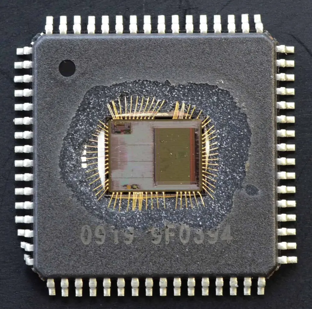
Ball grid array (BGA) packages have arrays of solder ball connections instead of leads, enabling high density interconnection with printed circuit boards (PCBs). However, the lack of visible leads and solder connections under the package presents challenges for hand soldering or reworking BGAs. Specialized techniques and tools are required. This article covers key BGA soldering considerations, processes, equipment and best practices for assembling, inspecting and reworking PCBs using BGA components.

What are BGA Packages?

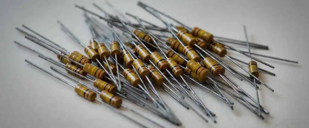
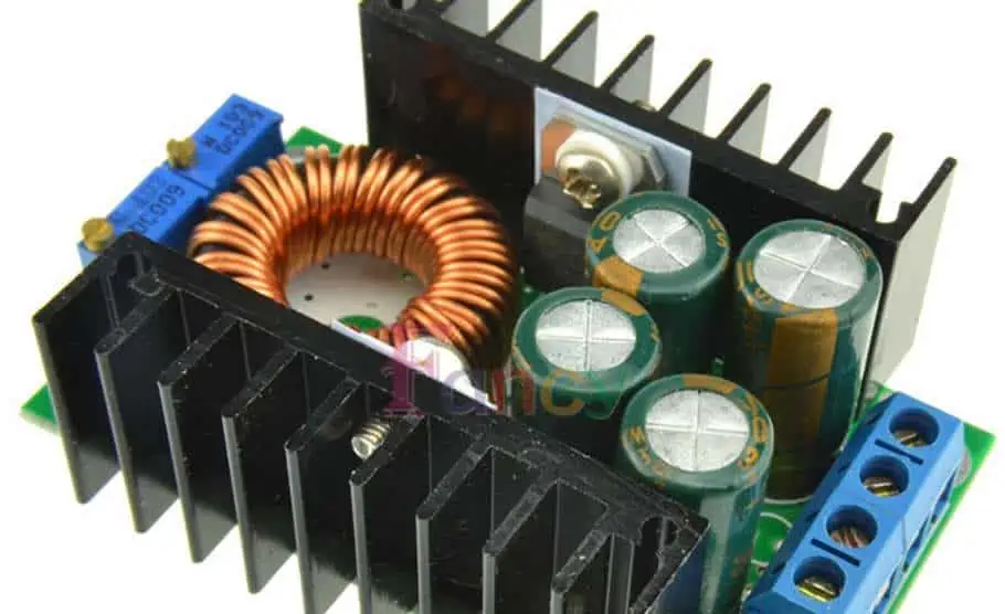
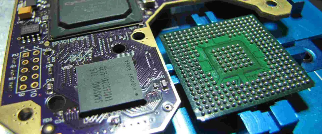
A ball grid array (BGA) integrated circuit package has an array of solder balls on the underside that connect to a matching grid of pads on a PCB surface. Some key characteristics:

  • Provides direct surface mount solder connections without visible leads
  • Ball pitch typically ranges from 0.5mm to 1.27mm
  • High density interconnections supporting large ICs with over 1000 pads
  • Often used for processors, ASICS, GPUs and chipsets
  • More challenging assembly and inspection vs leaded SMT components
  • Requires specialized rework equipment

The hidden solder joints under BGA packages mandate processes ensuring reliable interconnection.

Why Use BGA Packages?

BGA 0.4 MM Pitch

BGA packages provide several advantages over leaded chip packages:

  • Higher density interconnections from grid array
  • Shorter electrical paths with matched PCB layout
  • Smaller footprint maximizing board space
  • Reduces inductance improving high speed performance
  • Robust solid solder joints versus fragile leads
  • Direct surface mount assembly simplifies manufacturing
  • Lower profile and weight ideal for portables

The hidden solder balls allow BGAs to pack complex ICs into minimal space. But proper assembly practices are mandatory.

BGA Soldering Challenges

While enabling miniaturization, the lack of visible solder connections under BGA packages introduces challenges:

  • Inspecting assembly and alignment requires X-ray or special scopes
  • Reworking requires hot air or infrared no-contact methods
  • Tombstoning components risks damaging balls
  • Thermal stresses can crack joints under package
  • Aligning small components precisely is difficult
  • Voids hidden under package threaten reliability
  • Coplanarity across all balls must be tightly controlled
  • Environmental aging and moisture sensitivity risks

Special processes, equipment and materials help address these risks when working with BGAs.

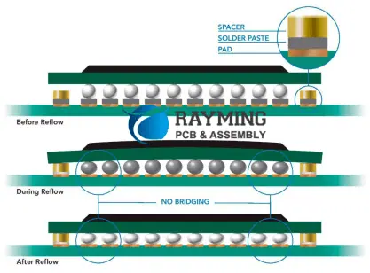
BGA PCB Land Patterns

IC Packages

The PCB pad pattern design supporting BGA packages requires attention to:

  • Match grid spacing to the BGA ball pitch
  • Pad diameter slightly larger than balls
  • Allow for positional tolerances
  • Include surrounding solder mask relief
  • Follow IPC guidelines for land dimensions
  • optionally omit mask over pads for more solder volume
  • Consider thermal pad size if present

Well-designed land patterns enable successfully mating BGAs during assembly.

BGA Solder Paste Printing

Applying solder paste for BGA components requires advanced stencils and processes:

Laser-cut Stencils

  • Precisely match PCB land pattern spacing
  • Allow paste printing down to 0.4mm pitch BGAs
  • Fine feature electroformed nickel/gold or stainless steel
  • Nanocoatings prevent solder balling

Print Processes

  • Miniature print heads deposit small paste volumes
  • Optical verification ensures paste in each aperture
  • Type 3 & 4 powders provide required viscosity
  • Stencil cleaning every 5-15 prints due to low volumes

Advanced stencils, pastes and printers enable printing tiny deposits aligned under each BGA ball.

BGA Component Placement

bga-rework-machine

Precision BGA component placement is critical due to tight positional tolerances:

  • High accuracy pick-and-place machine
  • Miniature placement nozzles matched to BGA size
  • Split optics and prism cameras enable precise alignment
  • Machine vision systems with pattern recognition
  • Component self-alignment during reflow reduces stress
  • Careful package handling to avoid solder ball damage

Automated optical inspection after placement verifies all BGAs are accurately positioned before reflow.

Reflow Soldering BGA Components

Applying heat to reliably solder BGA components requires following strict thermal profiles:

  • Preheat to allow component self-alignment
  • Soak above liquidus for thorough wetting
  • Rapid cool down after reflow to solidify joints
  • Bottom-side infrared heating ensures temperature uniformity
  • Maximum temperature limited to avoid damaging balls
  • Profile tailored for paste alloy and board/components

Carefully following thermal profile guidelines results in properly formed BGA solder joints.

BGA Solder Joint Inspection

Verifying BGA solder joint quality requires specialized inspection techniques:

  • Visual Inspection – Limited to examining exterior ball appearance and footprint registration.
  • X-Ray Inspection – Images through package reveal interior voids, cracks and shorts.
  • Acoustic Microscopy – Transmits sound waves revealing defects.
  • Automatic Optical Inspection – Scans entire assembly for package alignment issues.
  • Cross-Sectioning – Physically cutting sample joints to inspect internal structure.

Thorough inspection proactively identifies any latent BGA soldering defects before products leave manufacturing.

Troubleshooting Poor BGA Joints

Potential root causes of bad BGA solder joints include:

  • Misalignment between lands and balls
  • Insufficient solder paste volume or height
  • Solder ball defects or damage
  • Reflow thermal profile issues
  • Delamination between package and die
  • Moisture absorption under package
  • Thermal stress cracks
  • Contamination preventing wetting
  • Mechanical stresseswarping board

Finding and addressing the root cause is key before attempting BGA rework.

BGA Rework Process Overview

BGA Rework Services

Steps in a typical BGA component rework process:

Preparation

  • Review original assembly process for potential factors
  • Have replacement component and tools ready

Removal

  • Preheat board to reflow temperature
  • Use hot air nozzle to evenly heat entire area
  • Vacuum lift off or slide off component after complete reflow

Site Redressing

  • Clean pads thoroughly leaving no residue
  • Reapply flux to prepare for new balls
  • Potentially redress pads and land PCB land pattern

Reballing

  • Use stencil to apply new solder balls to BGA package
  • Reflow balls to attach to package terminals

Replacement

  • Use adhesive to temporarily secure component
  • Carefully realign new BGA on site
  • Reflow to form connections

Inspection

  • Verify alignment and ball connections
  • Assess any collateral damage to board or pads

Succesful BGA rework requires specialized tools, materials knowledge and process control.

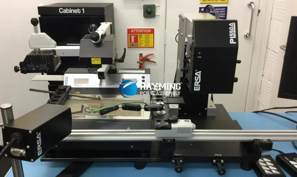
BGA Rework Equipment

Typical BGA rework equipment includes:

  • PCB Support Fixture – Secure board under component to prevent warping
  • Preheater – Gradually heats board to avoid thermal shock
  • Convection Rework Oven – For small boards requiring full oven thermal profile
  • Hot Air Nozzle – Directed heated air stream for localized heating
  • Temperature Control – Closed loop temperature control of nozzles
  • BGA Toolkit – Alignment guides, adhesive, fluxes, balls, stencil
  • Microscope – High magnification to inspect joints and alignment

Specialty rework tools enable properly removing and replacing BGAs with minimal collateral damage.

BGA Rework Process Considerations

Key factors for reliable BGA component rework:

  • Match ball alloy to original to avoid incompatibility
  • Adhesive tack strength must allow alignment tweaks
  • Bottom-side board preheating essential for even heating
  • Slow ramp rates prevent damaging balls or pads
  • Carefully follow thermal profile specifications
  • Use minimum required air flow rate
  • Lift BGA vertically without scrubbing
  • Use smallest nozzle size matching component

Well-developed process experience and procedures are critical for successfully reworking BGA components.

Summary of BGA Soldering Characteristics

Xilinx Zynq fpga
Xilinx Zynq fpga

Key characteristics for effectively soldering BGA packages:

  • Tight tolerance PCB land patterns match BGA balls
  • Advanced stencils and processes print small precise paste deposits
  • Robotic high precision die placement ensures alignment
  • Bottom-side IR heating allows gradual uniform reflow
  • Specialized tools needed for inspection after placement
  • BGA rework requires hot gas directed methods
  • Matching thermal profiles ensures reliable joint formation

By following the strict processes required for these hidden solder connections, reliable surface mount assembly is possible even for high density ball grid arrays.

Applications Using BGA Packages

FC-BGA (Flip Chip Ball Grid Array):

Some common applications leveraging BGA packages include:

  • Microprocessors and digital signal processors
  • Graphics and memory controllers
  • FPGAs, CPLDs, and ASICs
  • High pin count logic and interface ICs
  • RF circuits and mixed-signal controllers
  • Automotive engine control units
  • High frequency analog data converters
  • Image processing and communications chips

The small footprint and high interconnect density make BGAs ideal for many space constrained and high performance PCB assemblies across all electronics sectors.

Conclusion

While their hidden underside connections prevent visual validation, ball grid arrays remain essential component packages thanks to their compact size, interconnect density and electrical performance. By combining robust PCB design, tight process control, specialized SMT assembly equipment and inspection methods, reliable soldering and repair of BGA components is certainly achievable. Engineers working with BGAs must simply respect their unique demands. With extra care during design, assembly, handling and rework, the potential pitfalls of these headless devices can be effectively managed over the product life cycle.

Frequently Asked Questions

What are some signs of bad or faulty BGA solder joints?

Some symptoms that may indicate faulty BGA solder joints include:

  • Intermittent signal faults suggesting cracked joints
  • Overheating indicating poor heat conduction from die
  • Mechanical popping or cracking sounds during flexing
  • Inaccurate placement or shifting from expected position
  • X-ray or microscopic inspection revealing voids or cracks
  • Failure during drop testing or vibration exposure

Since joints are hidden, electrical faults and testing failures may be the first sign of underlying solder joint defects.

What are some methods to improve BGA solder joint reliability?

Strategies to enhance BGA solder joint reliability:

  • Optimize PCB land patterns for compliance to absorb stress
  • Utilize smaller ball pitches to increase joint density and redundancy
  • Improve solder masking around lands to strengthen pads
  • Specify BGAs with larger ball sizes to increase joint strength
  • Avoid excessive via-in-pad density under BGAs
  • Characterize optimal reflow profile to balance wetting and crack resistance
  • Specify BGAs with perimeter-array balls instead of full-grid for mechanical stability
  • Assess encapsulation underfills which reinforce solder joints

Reliability requires balancing many interdependent factors across IC, package, board, materials, components and process.

What defects could occur when reworking a BGA by hot air?

Some potential BGA rework defects when using hot air tools include:

  • Overheating adjacent components or board laminate materials
  • Heat shock damaging glass fabric or plated through holes
  • Oxidizing or de-wetting pads under package
  • Disturbing neighboring solder joints
  • Losing alignment tweaks when removing tool pressure
  • Inconsistently reflowing all balls and joints
  • Damaging or collapsing balls when sliding off component
  • Contaminating newly exposed surfaces needing redressing

Careful process development using thermocouples, thermal indicators and trial assemblies minimizes these risks.

A Define :BGA components and BGA soldering process

BGA (Ball Grid Array) appears as an evolution of PGA (Pin Prig Array). It is an Surface Mount Technology SMT (Link it to SMT articles). In the race of downsizing chips the need of high-density package technology increased, so pins become pads. These pads need to be soldered by solder balls. Weโ€™ll go through the advantages in BGA technology, the pcb soldering process and some difficult that appears on it.

YouTube video
How to Solder BGA Components Properly

BGA technology

BGA Technology for PCB Assembly ManufacturerInstead of leads BGA uses solder balls. This provides higher prototype SMT assembly reliability and allows to reach smaller balls pitch which increases the density of miniaturization. The balls pitch, distance from the center of one ball to the center of the next defines what type of BGA technology we are using. One millimeter pitch is standard BGA if we go smaller than that weโ€™re talking about micro-BGA. Micro-BGAs has pitches of 0.6, 0.4 and even 0.3 mm.

Each BGA would be identified by the number of sockets that contain, for example BGA 370 means 370 sockets. The BGA ic package contains a PCB on where the silicon die is placed, this is a high quality PCB like the one used for motherboards. Commonly uses fiber-reinforced material as BT substrate (Bismaleimide Triazine). When more flexibility is required polyimide tape is also available. Conductors are traces etched in copper foil bonded to a polymer substrate. Through-hole plated vias use allows several layer of interconnection.

BGAs are available in plastic or ceramic bodies, another option is metal-core BGA. Lower cost of plastic bodies make them more commonly used. Ceramic packages are vastly used for telecommunications, device-under-test equipment applications and laptops. Metal-core allows to use more circuitry than other options mentioned, mini-circuitry can be placed inside the BGA package, this an a addition to the regular number of balls and circuitry already there.

BGA Technology Advantages

We have strong reasons for choosing this technology, most of them are mentioned in the list below:

  • Higher pin density:We can now have  hundreds of pins on a single package without compromising quality of the soldering neither package reliability.
  • Lower inductance leads:unwanted inductance is directly proportional to distance, so less lead length provide us less unwanted inductance.
  • Better heat conduction:Less leads distances ensures less thermal resistance also providing as result better flow and conduction heat in between the two components that allows better conduction  heat through the board.
  • Increased performance:As a result of all advantages mentioned before combined. Better electrical performance compared to other IC packaging technologies. Also  provides superior performance at high speed.

BGA Package Disadvantages

  • Noncompliant connections:Since connection is made of solder balls instead of leads, this elements donโ€™t have flex capability therefore they are not mechanically compliant. Mechanical or thermal stress can fracture solder joints. Anyway, different techniques has already been applied to diminish this disadvantage. Just for naming one for example a compliant layer is added in the package that allows the balls to physically move in relation to the package.
  • Difficult inspection:Potential faults became difficult to identify and fix, since solder joint is not at the surface like in other assembly technologies. X-ray is needed for this type of inspection, this increases control time and costs.
  • Harder for prototyping and development instance:Imagine that using this type of solder for BGAs development is not practical, so sockets are used instead. Socket are unreliable
  • More expensive:The bumping process, the substrate and inspection costs become higher costs compared to a QFN package.

BGA Component Soldering Technologies

BGA Technology Advantages

A simple explanation of the BGA soldering process would be:

1. Solder paste is printed on pad array on PCB, this could be stencil or flux is coated onto pad.

2. Pick and place automated machine places BGA components onto PCB, here the alignment is critical.

3. PCB is ready to go reflow soldering in reflow soldering oven.

Key factors to consider in BGA soldering process

BGA Components storage

BGA are a thermal-sensitive and humidity components. The storage environment should be dry and temperature controlled.  Typically uses temperatures from 20ยฐC to 25ยฐC and less than 10%RH humidity. Nitrogen gas would be the recommended option.

BGA components should be used after 8 hours from pack opening. Ii is a common failure in the process to exceed this time limit. Baking temperature used is around 125ยฐC. A lower temperature will not achieve correct dehumidification, while higher temperature than needed could affect metallographic structure between solder balls and components

Stencil printing

PCB Stencils are made of stainless material, their thickness, aperture sizes and the use of frame or non-framed stencils is very important to ensure the proper and accurate dispensing of solder paste onto the board. stencil thickness should be limited within the common range from 0.12mm to 0.15mm, and laser cutted.

Too much paste could create shortcuts in between fine-pitch BGA balls and too little paste insufficient wetting and cold solder joints. Balancing the wetting by ensuring sufficient flux is needed. Pressure range will go from 35N to 100N and printing speed from 10 mm/s to 25 mm/s

Solder paste

Is essential in this process not only the quality of course but also the correct particle diameter should be chosen. Regarding quality we look forward to excellent printability and solderability, also less contaminant.

Solder particles need to be coherent with the pad and lead size. We could think that smaller the pitch smaller the particle but is not always so lineal this relation and particular considerations will be done in each case. As general recommendation solder paste below 45ฮผm particle diameter will cover both needs

BGA components placement and mounting

Accurate mounting here is criticall, although solder balls would self center we need to complete this operation with high precision. BGA/CSP rework station and chip mounter is used for this, precision of chip mounter reaches approximately 0.001mm. Solder can be  inspect, searching coplanarity defect and recognize some other defects such as missing balls. Local fiducial marks are set or a couple of fold lines are set as fiducial marks for manual inspection after assembly.

Going further in guarantee solderability, BGA components can be controled by 25.41ฮผm to 50.8ฮผm by height, also we applied during 400 ms a delay shutdown vacuum system. This way solder balls and solder paste contacts together and void soldering of BGA components can be decreased.

Reflow soldering

This is the most difficult phase to control, also a dificulting issue to attend is that BGA reflow temperature curves are not exactly the same in SMDs tan in BGAs. Temperature curve setting is crucial in the soldering joints forming process. So this would be something to really take care off.
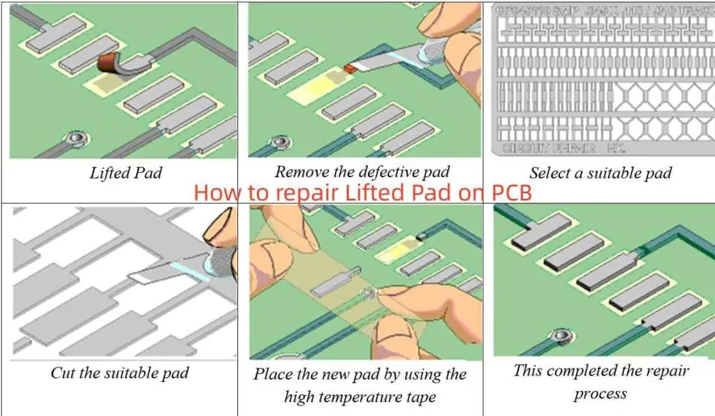
BGA rework

After soldering, process includes a rework station. Here each chip can be reworked independently  ion so that the BGA components can never be used again once they are disassembled from circuit board. A hot air reflux nozzle with the right size is used to cover the BGA area without affecting the surrounding components

BGA Soldering inspection

Different type of solder defects could appear. An open solder joint could be the result of insufficient temperature during reflow. This is because the existence of a non-collapsed ball. Also we could have intermittent connections, known as BICs (BGA Intermittent Connections). This will cause a aleatory failure very hard to detect once the PCB is fully assembled. Balls could be cracked causing short circuit or open circuit.

X-ray inspection in BGA technology

X-ray inspection in BGA technology

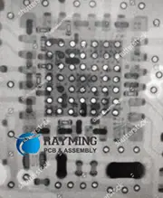
Since the joints are not on the surface, another method is necessary to guarantee quality, so X-ray technologies are applied. 2D inspections searches for cracks, bridging, bad  alignment or also insufficient solder. this is the low cost option. 5D X-ray solution will also compare the inspected PCB with the CAD file.We can analyze three individual slices between the BGA and solder balls, also get inside the solder  balls and deeply analyzes  the connection between the balls and the pad, Thus, our engineers can find flaws that with another technique would be impossible.

The Essential Role of Solder Mask in PCB Manufacturing: Types, Process & Standards

PCB hot air solder leveling

Solder Mask

Continue reading

What is Surface Mount Soldering?

PCB Assembly Introduction

Surface mount soldering (or SMD soldering) is the process of electrically and mechanically joining surface mount components (SMCs or SMT components) to printed circuit boards (PCBs) using solder. It enables automated assembly of miniature SMT components for electronics manufacturing. This article covers the key characteristics, processes, techniques and applications of surface mount soldering.

What is Surface Mount Technology (SMT)?

Surface mount technology (SMT) utilizes components that have terminations or “lands” that solder directly to matching pads on the surface of PCBs, as opposed to inserting leads into holes. Some benefits of SMT components include:

  • Smaller size – More compact, portable products
  • Faster automated assembly – Reduced manufacturing costs
  • Higher density – Complex circuitry fits into smaller spaces
  • Enhanced performance – Shorter connections, less noise and parasitics
  • Improved reliability and repeatability – Machined soldering vs. manual

SMT helped enable the electronics miniaturization and performance revolutions of recent decades. But it requires specialized soldering techniques tailored for small surface mount devices (SMDs).

What is Surface Mount Soldering?

SMT THT

Surface mount soldering describes the methods used to solder SMT component terminations onto matching conductive pads on a PCB surface utilizing specialized solder alloys and precisely controlled automated equipment. This creates both electrical connections and mechanical joints securing components.

Some defining characteristics of surface mount soldering include:

  • Typically performed by pick-and-place machines and reflow ovens
  • Requires bespoke pastes and precisely formed solder deposits
  • Adapted for leadless tiny device packages
  • Mandates tightly controlled thermal profiles
  • Mixes processes for array and discrete packages

The core objective of surface mount soldering is to rapidly produce high volumes of reliable solder joints on SMT boards. Next, we’ll look closely at the SMT soldering process steps.

Surface Mount Soldering Process Overview

A typical professional surface mount soldering process consists of five primary steps:

  1. Solder Paste Deposition – A solder alloy paste is precisely printed or dispensed onto pads on the PCB.
  2. Component Placement โ€“ Robotic pick-and-place machines position SMC components onto the solder paste deposits.
  3. Reflow – The board passes through a reflow oven melting the solder to attach components.
  4. Inspection – Automated optical inspection (AOI) validates joint quality.
  5. Rework – Any defective joints are repaired by reheating and reapplying solder.

Let’s explore each stage of the surface mount soldering process in more depth.

Solder Paste Application

Solder paste consists of a mixture of fine solder alloy particles and flux suspended in a thick medium. Solder paste must be applied in accurate locations with precise volumes and orientations. Two primary methods used include:

Printing – Screens or stencils with etched apertures align over boards. Solder paste forced through the openings prints exact deposits.

Jet Dispensing – Programmable valves directly jet paste droplets only where needed. Lower volumes but more flexibility.

Both printing and dispensing precisely deposit the small amounts of solder paste required for SMT components prior to placement.

SMT Component Placement

Electronic surface mount components are precisely positioned onto the applied solder paste using automated pick-and-place machines:

  • High speed robotic placement arms fetch components from feeders
  • Cameras visually identify part locations and alignment
  • Nozzles pick, orient and place components on target pads
  • Some devices require additional fluxes or adhesives
  • Different size nozzles or heads accommodate diverse components

Accurately placing a range of tiny SMCs is a sophisticated robotic process with tight tolerance requirements.

Solder Reflow Methods

Reflow soldering melts the deposited solder paste to wet component terminations and PCB pads forming solder joints:

  • Oven – Board conveyed through heated tunnel on conveyor
  • Hot Plate – Board heated on programmable hot plate
  • Laser – Directed beam targeting joints individually
  • Vapor Phase – Saturated vapor condenses only on board briefly

Most SMT production utilizes industrial convection reflow ovens to uniformly heat the assembly and reliably form millions of precise soldered connections.

Soldering Thermal Profiles

Reflow ovens follow optimized thermal profiles tailored to the board, components and solder paste:

  • Preheat – Gradually heats to avoid thermal shock
  • Soak – Dwell time allowing uniform temperature stabilization
  • Reflow – Above liquidus temperature to fully melt solder
  • Cool down – Controlled rate avoids disturbing joints

Profiles are precisely tuned to produce flawless solder joints across the populated PCB assembly.

Automated Inspection

Once soldering is complete, automated optical inspection (AOI) examines each joint:

  • High resolution cameras or lasers scan joints
  • Software compares to ideal profiles
  • Flags defects like shorts, opens, voids
  • Can integrate with rework station

Immediately identifying any insufficient joints enables quick reworking while the process is still hot.

Solder Joint Rework

Defective solder connections detected during AOI must be reworked:

  • Remove old solder first with solder wick if needed
  • Carefully heat joint with hot air tool
  • Use flux dispenser if necessary
  • Apply fresh solder paste and reflow
  • Clean any residues
  • Verify joints meet criteria

Proper rework corrects issues to restore high solder joint yield.

This overview of the surface mount soldering steps provides context on producing SMT assemblies in high volume production environments. Next, weโ€™ll focus on the critical soldering operations.

Key Aspects of Surface Mount Soldering

Several aspects of surface mount soldering require tight process control and oversight:

Solder Paste Mix

  • Powder particle size distribution
  • Powder shape – spherical preferred
  • Flux chemistry and activity
  • Viscosity and rheological behavior

Stencil Design

  • Aperture shapes and alignment
  • Stencil thickness and material
  • Print speed, pressure, separation

Component Placement

  • Accuracy within 0.05mm typically
  • Consistent pressure and orientation
  • Minimal rotation/skew
  • Avoiding tombstoning

Thermal Profile

  • Ramp rates, dwell times, peaks
  • Accounting for materials and geometries
  • Minimizing ฮ”T across assembly

Wetting and Microstructure

  • Pad and termination metallurgy
  • Ensuring dissolution and intermetallic formation
  • Rounded smooth fillets versus pointed peaks

Optimizing each step and interaction between processes ensures reliable solder joints.

Solder Paste Types

Specialized solder pastes have been developed for surface mount soldering applications:

No-Clean Solder Paste

  • Most common variety
  • Designed to not require cleaning after reflow
  • Reduces costs and processing steps

Water-Soluble Solder Paste

  • Allows easy paste removal after soldering
  • Ideal for rework or less common alloys

No-Slump Solder Paste

  • Thixotropic rheology prevents slumping
  • Useful for non-horizontal surfaces

Halogen-Free Solder Paste

  • Eliminates corrosive halogens like chlorine
  • Meets environmental regulations

Modern solder pastes are highly engineered materials tuned for the increasing demands of surface mount soldering.

Solder Paste Printing

Printing solder paste requires optimized stencil design and tightly controlled processes:

Laser Cut Stencils

  • Precisely cut apertures etched to match pads
  • Allow very fine pitch prints down to 01005 components
  • Clean laser cut edges prevent paste retention

CNC Cut Stencils

  • Economical method for prototyping
  • Limited on fine features below 0402 size

3D Printed Stencils

  • Enables high mix, fast turnaround
  • Challenging getting adequate aperture accuracy

Step Stencils

  • Separate stencils for pastes requiring different volumes

Nanocoated Stencils

  • Low surface energy coating prevents paste sticking
  • Allows easier print deposit alignment

With robust stencil design and printing processes, paste can be deposited accurately even for microscopic components.

Surface Mount Components

Billions of different specialized surface mount components are manufactured for electronics assembly. Some major categories include:

Passives – Resistors, capacitors, inductors and transformers. Common package sizes down to 0201 or smaller.

Actives – ICs, transistors, diodes, LEDs, etc. Wide variety of package types from large BGAs to tiny QFNs.

Connectors – High density board-to-board connectors including mezzanine and edge mount.

Electromechanical – SMT switches, relays, buttons, sensors, crystals, clocks etc.

Interposers – Adapters to integrate non-surface mount components.

Continued miniaturization and expanding package options enables placing more functionality into each square millimeter.

Solder Paste Inspection

Solder paste stencil frame

After printing but before component placement, the applied solder paste deposits are typically inspected:

2D Paste Inspection

  • Color cameras compare print outcomes to ideal
  • Verify positioning, offsets, rotations
  • Check for bridging, insufficient volumes

3D Solder Paste Inspection

  • Laser or photogrammetry scanning
  • Generates detailed 3D paste volume profile
  • Measures paste heights across entire area

Paste inspection helps confirm the print process is dialed in before committing components.

Pick-and-Place Machines

High speed pick-and-place (PnP) machines precisely populate printed circuit boards:

  • Utilize multiple placement heads for productivity
  • Cameras identify part locations and orientations
  • Vacuum nozzles pick components from feeders
  • Robotic arms rapidly place parts onto pads
  • Advanced models incorporate artificial intelligence

High end PnP machines can place over 120,000 components per hour with accuracy down to 0.030mm. This enables automated assembly of SMT boards containing thousands of unique parts.

Reflow Soldering Methods

In addition to thermal profiling, different reflow techniques suit certain applications:

Infrared Reflow

  • IR heaters or lasers solder small assemblies
  • Limited by slower process speed

Vapor Phase Reflow

  • Condensation uniformly heats small boards
  • Minimal overheating or thermal shock

Laser Soldering

Induction Soldering

  • Magnetic field induced eddy currents melt solder
  • Contactless, localized heating

There are many options to deliver tightly controlled thermal input and form high quality soldered interconnections.

Solder Joint Inspection

Beyond visual inspection during assembly, automated optical inspection (AOI) is routinely performed:

2D AOI

  • Color cameras image entire assemblies
  • Checks for missing, misaligned or faulty components
  • Flags collapsed, bridging or shorted joints

3D AOI

  • Laser or photogrammetry scanning
  • Generates detailed 3D surface map
  • Measures volumes, standoff heights and coplanarity

AOI immediately identifies any insufficient joints requiring rework.

Lead-Free Soldering Challenges

Switching to lead-free solders introduced new processing challenges:

  • Higher melting temperatures stress components
  • Poorer wetting increases difficulty forming reliable joints
  • Oxidation and intermetallic growth impact reliability
  • Reduced fatigue resistance risks future failures
  • Tin whiskering can cause electrical shorts
  • Narrower process windows mandate tight control

Through experience and research over the past two decades, the industry has largely mastered lead-free soldering to achieve comparable longevity to leaded solder processes.

Summary of Surface Mount Soldering Attributes

In summary, core attributes of surface mount soldering:

  • Enables automated manufacturing of electronics assemblies with SMT components
  • Requires specialized solder paste materials and deposition processes
  • Leverages advanced robotic technology for precision component placement
  • Controlled thermal profiling ensures melting and wetting to create joints
  • Automated inspection identifies any defects needing rework
  • Process tightly controlled to ensure small components are reliably soldered

Continuous improvement in SMT soldering has helped enable ongoing electronics miniaturization and performance gains.

Applications of Surface Mount Soldering

Surface mount soldering is utilized across virtually all electronics sectors:

Consumer Electronics – Cellphones, laptops, home appliances, gaming systems, etc.

Telecommunications – 5G infrastructure, network switches, servers.

Automotive – Engine control units, infotainment, driver assistance.

Medical – Patient monitors, imaging systems, prosthetics.

Aerospace/Defense – Avionics, guidance systems, communications.

Industrial – Programmable automation controllers and robotics.

Any application where small, lightweight, high performance electronics are advantageous leverages the capabilities enabled by surface mount soldering.

Frequently Asked Questions

What are some key differences between surface mount soldering and through-hole soldering?

Key differences between SMT soldering and through-hole soldering include:

  • SMT is automated while through-hole is manual
  • SMT uses precisely applied paste while through-hole dips or waves
  • SMT requires ovens for reflow while through-hole uses irons
  • SMT requires specially formulated solder while through-hole uses wire
  • SMT allows miniature components vs. through-holeโ€™s larger sizes

The automated precision of SMT enables modern miniature electronics assemblies.

What defects commonly occur with surface mount soldering?

Common SMT soldering defects include:

  • Insufficient solder or dry joints
  • Excessive voiding in solder joints
  • Cold or fractured solder joints
  • Bridging between adjacent joints
  • Solder balls or splatter
  • Overheated, burnt or lifted pads
  • Tombstoning or drawbriding of components

Tight process control during pasting, placement and reflow minimizes defects.

What are some key tips for hand soldering SMT components?

Tips for manually hand soldering SMT parts:

  • Use a fine tip suitable for the component size
  • Carefully control soldering iron temperature
  • Use miniature solder wire or premixed paste
  • Apply flux to enable good wetting
  • Avoid overheating parts or lifting pads
  • Visual inspect joints for acceptable fill and fillets

Though challenging, with proper tools and technique SMT components can be hand assembled successfully.

What is Zero Ohm Resistor ?

A zero ohm resistor, also called a zero ohm jumper or link, is a resistor with a designed resistance of, or very close to, zero ohms. Despite having negligible resistance, these devices serve important functions in circuit boards. This article covers the characteristics, symbol, typical applications, PCB layout considerations, and substitutes for zero ohm resistors.

Zero Ohm Resistor Characteristics

A zero ohm resistor looks identical to a standard through-hole or SMD resistor. However, it is constructed to provide the lowest possible resistance, ideally 0 ohms. Key characteristics include:

  • Resistance range from 0.0ฮฉ to 0.1ฮฉ typically
  • Rated for various power levels per size
  • Through-hole, SMD and chip package types
  • Act as short circuits or jumpers when soldered
  • Provides connection without copper trace
  • Lets PCB layout be adjusted post-production

Zero ohm resistors are extremely useful for flexibly bridging connections during prototyping, reworking boards, or adjusting circuit layouts as needed.

Zero Ohm Resistor Symbol

Zero ohm resistors are represented on circuit schematics using a standard resistor symbol with the resistance value labeled as 0ฮฉ:

This indicates any location a zero ohm resistor is used to short two points together in the actual circuit.

On PCB layouts, zero ohm resistors are denoted using unique layer silkscreen identifiers defined in the legend. Common identifiers include:

  • Component overlay: 0ฮฉ
  • Top silkscreen: JMP
  • Bottom silkscreen: BRIDGE

This allows PCB assembly operators to clearly identify which components act as intentional shorts.

Why Use Zero Ohm Resistors?

Zero ohm resistors provide several advantages versus just connecting points with traces:

Adjust Layout Post-Fabrication

  • Can solder or omit zero ohm resistors to alter connections
  • Facilitates field upgrades, prototyping, and reworking boards

Simplify Routing

  • Avoids crossing complex traces on dense boards
  • Jumps between layers can be made post-production

Improve manufacturability

  • Fine pitch ICs have space for resistors but not traces
  • Simplifies via placement

Maintain Part Count

  • Substituting for jumpers keeps BOM part quantity same
  • Easier pick-and-place assembly programming

Emulate Fuses/Thermistors

  • Act as resettable fuses when sized properly
  • Can act as temperature sensitive resistors

Zero ohm resistors empower more flexible PCB layouts and post-production adjustments.

Common Applications of Zero Ohm Resistors

Typical use cases for zero ohm resistors include:

Bridging Connections

  • Shorting points like unused IC pins
  • Providing test points to isolate sections
  • Paralleling supply rails

Adjusting Circuits

  • Enabling/disabling options post-production
  • Converting oscillator types
  • Selecting different gain settings

Simplifying Traces

  • Avoiding dense routing blockages
  • Jumping between layers as needed
  • Connecting ground planes

Physical Support

  • Anchor points for wires or connectors
  • Securing points needing strain relief
  • Spacing heavy components

Zero ohm resistors empower designers to optimize PCB layouts while retaining flexibility.

PCB Layout Considerations for Zero Ohm Resistors

To leverage zero ohm resistors most effectively, keep these PCB design guidelines in mind:

  • Clarify purpose using silkscreen identifiers like 0ฮฉ or JMP
  • Place at locations requiring post-production shorts
  • Substitute for jumpers to keep BOM clean
  • Use to simplify routing without crossing traces
  • Avoid shorts from solder, especially on dense boards
  • Include some extras for rework flexibility
  • Follow datasheet guidelines for power ratings
  • Review if any can be replaced by direct traces

Carefully planning locations for zero ohm resistors during layout facilitates optimizing the design iteratively even after fabrication.

SMT Zero Ohm Resistor Types

Several different SMT zero ohm resistor package styles exist:

2512

  • Length 3.2mm x Width 1.6mm
  • Rectangular, double terminals
  • Rated up to 1W

0402

  • Length 1mm x Width 0.5mm
  • Tiny surface mount device (SMD)
  • Rated roughly 0.1W

0603

  • Length 1.6mm x Width 0.8mm
  • Very small SMD package
  • Rated around 0.25W

0805

  • Length 2mm x Width 1.25mm
  • Popular mid-size SMD
  • Rated up to 0.5W

1206

  • Length 3.2mm x Width 1.6mm
  • Larger SMD, similar to 2512
  • Rated up to 0.5W

Larger or higher power ratings are physically more robust. But smaller SMD footprints save valuable space.

Through-Hole Zero Ohm Resistor Types

100K-Resistor

Common through-hole zero ohm resistor packages include:

Axial Leaded

  • Cylindrical body with wire leads
  • Often 5% tolerance flameproof types
  • Rated up to 3W typically

Radial Leaded

  • Discoidal ceramic body with bent leads
  • Available up to 5W power rating
  • Commonly with 5% tolerance

Metal Film

  • Cylindrical coated metal film structure
  • Very low resistance material (<10mฮฉ)
  • Lower power, around 0.5W

Fusible

  • Wirewound or metal strip construction
  • Designed to burn out if overloaded
  • Used like resettable fuses up to 35W

Through-hole zero ohm resistors support higher current connections.

Alternatives to Zero Ohm Resistors

In some situations, alternatives to zero ohm resistors may be preferable:

PCB Traces

  • Simplest direct board shorts
  • Limit adjustments post-production
  • Lowest resistance via thick copper

Wire Jumpers

  • Easily modified or replaced
  • Allows off-board connections
  • No PCB space required

Test Points

  • Facilitates voltage probing
  • Isolates sections of circuit
  • Extra components not needed

Solder Bridges

  • Direct solder shorts for quick mods
  • Can reconnect blown fuses
  • Risks accidental connections

Fuse Clips

  • Accepts replaceable fuses
  • Resets protection after failure
  • More robust than zero ohm links

Each approach has trade-offs to evaluate for the particular application.

Summary of Zero Ohm Resistor Characteristics

To summarize, the key characteristics of zero ohm resistors:

  • They are standard resistors made with very low (<0.1ฮฉ) resistance.
  • On schematics they are shown as standard resistors labeled with 0ฮฉ value.
  • They act as short circuit connections when soldered on PCBs.
  • They enable flexible post-production adjustments of connections.
  • SMD and through-hole packages support sizes up to several watts.
  • Alternatives like traces or wire jumpers have advantages in some applications.

Zero ohm resistors empower modification, rework and simplified routing of PCB layouts. Understanding their applications helps designers optimize prototyping and production.

Frequently Asked Questions

Resistor color

What are some good rules of thumb for using zero ohm resistors versus traces or jumpers on a PCB?

General guidelines on when to use zero ohm resistors versus alternatives:

  • Use traces for simple point-to-point shorts and ground connections
  • Use jumpers for temporary prototypes or off-board connections
  • Use zero ohms when post-fab adjustments may be needed
  • Use zero ohms when complex trace routing is difficult
  • Use zero ohms to keep BOM cleaner over jumpers
  • Use traces when shorts are unlikely to require changes

Evaluate trade-offs on a case-by-case basis for each connection.

What power rating should you choose for a zero ohm resistor?

Select a zero ohm resistor power rating according to:

  • Expected continuous current through the connection
  • Peak pulsed or inrush current if applicable
  • Desired safety margin or headroom
  • Physical space available on PCB
  • Thermal environment and airflow

A good practice is choosing a rating 2-3x the expected current to provide robustness.

What are common causes of failure for zero ohm resistors?

Zero ohm resistors most often fail due to:

  • Overcurrent exceeding power rating
  • Accumulated pulse heating degrading connections
  • Thermal stresses fracturing solder joints
  • Mechanical stresses from vibration/shock
  • Nearby short circuits passing excessive current
  • Faults in connected circuitry

Proper sizing, layout and assembly mitigate these failure modes for reliable operation.

12 Functions of Zero Ohm (ฮฉ) Resistance

We often see 0 ohm resistors in the circuit. For newcomers, it is often confusing: since it is a 0 ohm resistor, it is a wire. Why should it be installed? Is there such a resistor sold in the market? In fact, the resistance of 0 ohms is quite useful.

YouTube video

Zero ohm resistor, also known as jumper resistor, is a special purpose resistor. The 0 ohm resistor is not really zero resistance (that is the superconductor dry thing), just because of the resistance, it is also a regular paste. The chip resistor has the same error accuracy as this indicator.

The following summarizes a series of usages of zero ohm resistors:

1. There is no function in the circuit, just for the convenience of debugging or compatible design on the PCB.

2. Can be used for jumpers, if a certain line is not used, you can directly not attach the resistor (does not affect the appearance)

3. When the matching circuit parameters are uncertain, replace it with 0 ohms. When the actual debugging is performed, determine the parameters and replace them with specific numerical components.

4. When you want to measure the current consumption of a certain part of the circuit, you can remove the 0ohm resistor and connect the ammeter to facilitate the current consumption.

5. In the wiring, if the actual cloth can not pass, you can also add a 0 ohm resistor

6. Act as an inductor or capacitor under high frequency signals. (related to external circuit characteristics) Inductive use, mainly to solve EMC problems. Such as ground and ground, power and IC Pin.

7. Single point grounding (refers to protective grounding, working grounding, and DC grounding are separated from each other on the equipment, and each becomes an independent system.)

8. Fuse action.

9. Ground and digital ground single point grounding.

As long as it is ground, it will eventually be received together and then into the earth. If they are not connected together, they are โ€œfloatingโ€, there is a pressure difference, and it is easy to accumulate electric charges and cause static electricity. The ground is referenced to 0 potential, all voltages are derived from reference ground, the ground standards are the same, so the various grounds should be shorted together.

It is believed that the earth can absorb all the electric charges and always maintain stability, which is the ultimate ground reference point. Although some boards are not connected to the earth, the power plant is connected to the earth, and the power supply on the board will eventually return to the power plant. If the analog ground and the digital ground are directly connected to each other, it will cause mutual interference. It is not short-circuited and not appropriate. There are four ways to solve this problem as above:

(1) Connected by magnetic beads;

(2) Connected by a capacitor;

(3) Connected by an inductor;

(4) Connect with a 0 ohm resistor.

The equivalent circuit of the magnetic bead is equivalent to the band-stopper, which only significantly suppresses the noise of a certain frequency point. When using it, it is necessary to estimate the noise frequency in advance so that the appropriate model can be selected. For cases where the frequency is uncertain or unpredictable, the beads do not fit.

The capacitor is connected straight to the ground, causing floating.

The inductor is bulky, has many stray parameters, and is unstable.

The 0 ohm resistor is equivalent to a very narrow current path, which effectively limits the loop current and suppresses noise. The resistor has an attenuation in all frequency bands (0 ohm resistor also has impedance), which is stronger than the magnetic beads.

The following two figures are a circuit, just because the electronic components are not labeled the same. R7 (R33) is a single-point link end for analog ground and digital ground.

12 Functions of Zero Ohm (ฮฉ) Resistance

10. For current circuit when bridging

When the ground plane is divided, the shortest return path of the signal is broken. At this time, the signal loop has to be detoured to form a large loop area, and the influence of the electric field and the magnetic field becomes stronger, which is easy to interfere/interfere. By connecting a 0 ohm resistor across the partition, a shorter return path can be provided to reduce interference.

11. Configuration circuit

Generally, there should be no jumpers or dip switches on the product. Sometimes the user will tamper with the settings, which may cause misunderstanding. In order to reduce the maintenance cost, the 0 ohm resistor is used instead of the jumper to solder on the board.

The vacant jumper is equivalent to the antenna at high frequencies, and the effect of the chip resistor is good.

12. Other uses

Overlay when wiring;

Debug/test;

Temporarily replace other patch devices;

As a temperature compensation device;

More often than not, it is due to EMC countermeasures. In addition, the 0 ohm resistor is less than the parasitic inductance of the via, and the via also affects the ground plane (because the hole is to be dug).

There is also a different size 0 ohm resistor to allow different currents, generally 0603 1A, 0805 2A, so different currents will choose different sizes, there are reserved positions for magnetic beads, inductors, etc., according to magnetic beads, inductors The size is also packaged, so 0603, 0805 and other different sizes are available.

What is Buck Converter

A buck converter is a switched-mode DC-DC converter that steps down a higher input voltage to a lower output voltage. By quickly switching a series transistor on and off, voltage is converted efficiently without requiring a linear regulator’s power dissipation.

This article provides a comprehensive overview of buck converter operating principles, design considerations, key parameters, common applications, and integration into larger systems. After reading, you will understand exactly what role buck converters serve in regulated power supplies.

Buck Converter Basics

A buck converter, also called a step-down converter, performs DC-DC conversion from a higher input voltage to a lower output voltage. For example, converting 12V to 5V or 48V to 1V.

Key characteristics of a basic buck converter circuit:

  • Converts DC input to a pulsing stepped waveform
  • Smooths output with an LC filter
  • Wastes less power vs. linear regulation
  • Output voltage is a function of duty cycle
  • Requires just four main components
  • Very efficient (up to 95%)

The buck topology is popular due to its simplicity, efficiency, compact size and flexibility. Let’s examine the internal circuitry and operation.

Buck Converter Circuit Operation

YouTube video

A basic buck converter contains four primary components:

Switch / Transistor (M1) โ€“ The transistor acts as a switch, turning on and off rapidly to chop the input voltage. A power MOSFET is commonly used due to its fast switching speed and minimal loss.

Diode (D1) โ€“ The diode provides a return current path for the inductor when the transistor switch is off. Schottky diodes are frequently used for their fast recovery times.

Inductor (L1) โ€“ While the switch is on, the inductor stores energy in its magnetic field. This energy transfers to the load when the switch turns off.

Capacitor (C1) โ€“ The capacitor smooths voltage ripple at the converter output for steady, regulated DC.

Now let’s walk through a complete switching cycle to see how these components interact to convert and regulate voltage.

Buck Converter Switching Cycle Analysis

The buck converter regulates output voltage by rapidly switching the transistor on and off. This drives the connected inductor to store and release energy to the load in a controlled manner. Each cycle involves two distinct circuit states:

Switch ON State

In the ON state, the transistor switch is closed allowing current to flow from the input source to the inductor:

  • Input voltage is applied directly across the inductor
  • Inductor current ramps up linearly, storing energy in a magnetic field
  • Load current is supplied by the capacitor
  • Diode is reverse biased blocking current flow

Switch OFF State

In the OFF state, the transistor switch opens interrupting current flow:

  • Inductor magnetic field collapses, maintaining current flow
  • Stored inductor energy transfers to the load
  • Diode becomes forward biased, providing a return path
  • Capacitor charges from the inductor/diode

Rapidly alternating between these two states generates a pulsed output voltage. The relative ON vs. OFF durations determine the average output voltage.

Buck Converter Duty Cycle

The output voltage of a buck converter is proportional to the duty cycle D of the switching transistor.

Duty cycle D is defined as:

D = Ton / (Ton + Toff)

Where:

  • Ton = Time switch is ON
  • Toff = Time switch is OFF
  • Ton + Toff = Total switching period

For example, with Ton = 5us and Toff = 15us:

  • Total period is 20us
  • Duty cycle D is 25% (5us / 20us)
  • Output voltage is 25% of input

This demonstrates the buck converter’s step-down effect – by rapidly switching with a low duty cycle, high voltages can be converted to much lower regulated outputs.

Buck Converter Voltage Transfer Function

The relationship between buck converter input voltage (Vin), output voltage (Vout) and duty cycle is:

Vout = D * Vin

Where D is the duty cycle between 0 and 1.

This means the output voltage is equal to the duty cycle multiplied by the input voltage.

If Vin = 12V and D = 0.25, then Vout is 0.25 * 12V = 3V

This shows how the buck converter steps down based on duty cycle. The voltage transfer function is key to designing a buck regulator.

Buck Converter Benefits and Drawbacks

Advantages of buck converters include:

  • High efficiency, up to 95% with low loss
  • Compact, simple circuitry
  • Flexible output adjustment via duty cycle
  • No minimum load required
  • Isolated designs possible for safety

Limitations can include:

  • Output voltage must be less than input voltage
  • Switching noise may require filtering
  • High current inductors may be bulky
  • Heat sinking required at high currents
  • Complex control loops for best performance

Overall, buck regulators provide an excellent balance of efficiency, flexibility and simplicity. Now let’s examine some key design considerations.

Buck Converter Design Considerations

Some important buck converter design factors include:

Input Voltage Range โ€“ The maximum and minimum input voltage specification ensures the buck converter operates over the intended supply range.

Output Voltage โ€“ The required steady-state output voltage. Lower output voltages require lower duty cycles.

Output Current โ€“ The maximum load current helps size the inductor, diode, capacitor and transistor ratings.

Switching Frequency โ€“ Higher frequencies allow smaller inductors and capacitors but increase switching losses. Optimize for efficiency and size.

Transient Response โ€“ The allowable overshoot/droop during sudden load changes guides compensation network design.

Carefully considering these parameters ensures the buck converter is designed properly for the particular application requirements.

Selecting Buck Converter Components

The four main buck converter components must be selected properly for the design specifications:

Transistor โ€“ Select based on required current handling, voltage rating, RDS(ON) resistance, and switching speed. Include margin above maximum load current.

Inductor โ€“ Size inductance based on desired current ripple. Higher value gives lower ripple but larger size. Rated for peak switch current plus margin.

Diode โ€“ Rated for maximum load current. Fast recovery time Schottky diode. Low forward voltage drop improves efficiency.

Capacitor โ€“ Output capacitance reduces voltage ripple. Higher capacitance gives lower ripple. ESR impacts transient response.

Dimensioning components for reliability under worst-case operating conditions ensures robust performance over the product lifetime.

Buck Converter Design Example

The Flyback Converter Topology

Let’s walk through an example buck converter design to see the component selection process:

Design Requirements

  • 12V nominal input voltage (9 – 15V range)
  • 5V regulated output voltage
  • 3A maximum load current
  • 400kHz switching frequency

Inductor Selection

  • Pick 10% peak-to-peak inductor current ripple
  • Delta I = 0.1 * Imax = 0.3A ripple
  • Calculate minimum inductance
  • Lmin = (Vin – Vout) * (Vout / f * DeltaI) = 68uH
  • Choose 100uH rated for 3.5A+

Capacitor Selection

  • Target < 5% output voltage ripple at 400kHz
  • Delta V = 0.05 * Vout = 250mV
  • Imax ripple = 3A
  • Cmin = Imax / (8 * f * DeltaV) = 30uF
  • Select low ESR cap rated for margin above Imax

Transistor Selection

  • Peak current = Imax + 1/2 DeltaI = 3.15A
  • Select MOSFET with >4A rating and low RDS(ON)
  • Include heatsink rated for power dissipation

Diode Selection

  • Schottky diode rated for Imax plus margin
  • Low forward voltage type

This example provides a simplified overview of the core component selection process for a basic buck converter design.

Buck Converter Control Methods

To achieve stable, responsive output voltage regulation, buck converters employ closed-loop control:

Voltage Mode

  • Measures output voltage with feedback divider
  • Controls duty cycle to maintain voltage
  • Susceptible to instability

Current Mode

  • Adds inductor current sensing
  • Prevents subharmonic oscillation
  • Improves transient response

Hysteretic Control

  • Switches based on output ripple bandwidth
  • No compensation loop required
  • Can cause variable frequency

PID

  • Actively tunes proportional, integral and derivative gains
  • Dynamic compensation for wide loads
  • More complex to implement

Advanced control techniques like digital PID allow buck regulators to adaptably maintain tight voltage regulation.

Buck Converter Parameters and Characteristics

Key buck converter parameters help evaluate performance:

Efficiency โ€“ Ratio of output power to input power, with ideal up to 95%.

Ripple โ€“ Remaining AC voltage and inductor current fluctuations.

Load Regulation โ€“ Output voltage change based on load current variation.

Line Regulation โ€“ Output change based on input voltage change.

Transient Response โ€“ Overshoot and settling time for step load changes.

Test results for these parameters validate the regulator design and PCB layout optimize overall functionality.

Buck Converter Applications

Frequency converter PCBA Boards

Buck converters are ubiquitously used to step-down and regulate voltages in a wide range of applications:

  • DC power supplies
  • Battery chargers
  • LED drivers
  • Point-of-load regulators on PCBs
  • DC-DC conversion in electric vehicles
  • High current load regulation
  • Pre-regulators for LDOs
  • Envelope tracking RF amplifiers

Any application with higher DC input voltages and lower DC load voltages can benefit from the simplicity, efficiency and compact size of properly designed buck converter circuits.

Integrating Buck Converters Into Systems

Buck regulators are commonly integrated within larger electronic systems:

Input Filtering โ€“ An input pi filter reduces EMI and voltage ripple from the upstream power source.

Protection Devices โ€“ Fuses, thermistors and TransZorbs clamp overcurrent and transients on input and output.

Feedback Compensation โ€“ An op amp may generate the PWM signal sent to the transistor based on voltage feedback.

Paralleling Converters โ€“ Buck regulators can be paralleled using diodes for higher output currents.

Sequencing โ€“ Where multiple voltage rails must be powered on/off in order, power sequencing ICs control regulator timing.

Properly incorporating buck converters into the greater design ensures robust performance meeting all system requirements.

Summary of Buck Converter Function and Applications

The key points regarding buck converter function and applications covered here include:

  • Buck converters step down a higher input DC voltage to a lower regulated output voltage efficiently by rapidly switching the input power on and off.
  • Regulation is achieved by adjusting the switching duty cycle to maintain the intended output voltage based on feedback.
  • Only four primary components are required – a transistor, diode, inductor and capacitor – making buck regulators simple and cost effective.
  • Careful component selection and control loop design ensure proper voltage conversion and regulation for the intended application over expected operating conditions.
  • Buck converters are ubiquitous DC-DC converter circuits used across countless applications due to their simplicity, flexibility and high efficiency.

Hopefully this overview clearly explains what role buck converters serve in regulated power supplies and inspires further learning about their design and integration.

Frequently Asked Questions

What are the main advantages of a buck converter vs. an LDO?

Key advantages of buck converters compared to low dropout (LDO) linear regulators include:

  • Far higher efficiency – up to 95% vs. <50% for LDOs
  • Can output high load currents – tens of amps vs. one amp or less
  • Wastes less power as heat enabling smaller size
  • Lower cost at higher currents
  • Higher input to output voltage differential – step-down vs. just small dropout

So for most higher power applications, buck converters are superior to LDOs.

What are some key disadvantages or limitations of buck converters?

Some potential downsides of buck converters include:

  • Output voltage must be lower than input voltage
  • Switching can produce noise needing filtering
  • Inductor core losses reduce efficiency at high frequencies
  • Require proper control loop design for stability
  • Higher BOM cost than linear regulators

So buck converters may not be ideal for very low noise or ultralow power circuits.

What determines the maximum switching frequency for a buck converter?

Key factors limiting buck converter switching frequency include:

  • MOSFET switching losses start exceeding conduction losses
  • Gate charges and transition times of transistors
  • Core losses in inductor material due to hysteresis
  • Capacitor equivalent series resistance and inductance
  • Feedback circuit bandwidth limitations
  • EM radiation becoming problematic

Practical switching frequencies for buck regulators generally range from 100 kHz to 5 MHz at most. Minimizing loss mechanisms allows pushing to higher frequencies for smaller size.

Full Introduction About IC Packages Types and Functions

IC Packages

Integrated circuits (ICs) incorporate miniaturized electronic components fabricated together into a single chip. To connect, protect and support these fragile silicon dies, they are enclosed in a container known as an IC package. Various standardized package types have evolved to suit different IC applications and assembly methods. This article provides a comprehensive overview of popular IC package classifications, structures, materials, functions and manufacturing processes.

IC Package Role and Classification

An IC package serves several essential functions:

  • Protects vulnerable silicon die from physical, electrical or environmental damage
  • Provides mechanical support and structure for handling
  • Supplies external electrical connections via leads or pads
  • Facilitates heat dissipation away from the die during operation
  • Allows the IC to be integrated onto a printed circuit board (PCB)

IC packages can be classified based on:

  • Lead/connection types โ€“ through-hole, surface mount
  • Package material โ€“ plastic, ceramic, metal
  • Pin count โ€“ number of leads or pads
  • Die mounting โ€“ pin grid array, ball grid array
  • Package outline dimensions and standards

By understanding package characteristics, engineers can select optimal configurations for each IC application.

Through-Hole IC Packages

Early ICs used packages with metal leads or pins that passed through holes on the PCB to make electrical and mechanical connections. These through-hole (PTH) packages include:

DIP (Dual In-line Package)

The venerable DIP, introduced in 1964, has two parallel rows of through-hole pins projecting from the long edges of a narrow rectangular plastic or ceramic body. Common variations:

  • DIP โ€“ Dual In-line Package, 2+ pins
  • CDIP โ€“ Ceramic DIP, widespread until the 1990s
  • PDIP or Plastic DIP โ€“ Inexpensive molded plastic package
  • Narrow DIP – More compact with 0.3โ€ row spacing

DIPs can contain anywhere from 4 to 64 pins. The large, through-hole leads provide robust mechanical connection but limit component density on PCBs. DIPs are still used for moderate complexity ICs like microcontrollers where larger packages are acceptable.

TO โ€“ Transistor Outline

Originated for packaging individual transistors, the TO package has evolved into a diverse, expanding family for ICs:

  • TO-92 โ€“ Small, low-power, plastic, 3-leaded package often used for transistors.
  • TO-126 โ€“ Larger plastic power package with a metal tab for heatsinking
  • TO-220 โ€“ Widely used metal can-type package able to dissipate substantial heat
  • TO-247 / TO-3P โ€“ Large metal package with screw mounting for high power levels
  • TO-263 / D2PAK / SOT-223 โ€“ Smaller surface-mountable TO style package

TO packages are valued for efficient power dissipation and low cost. However, their size can limit PCB space efficiency versus newer SMT packages.

Quad Packages

Quad packages have four rows of through-hole leads extending from the underside of a square plastic or ceramic body. Two popular variations are:

  • QFP (Quad Flat Pack) – Four sides of leads in gull wing shape; up to 208 pins
  • PQFP (Plastic Quad Flat Pack) – Molded plastic version of QFP with lower cost

With high pin counts in a compact space, QFPs were widely used for microprocessors and ASICs until surface mount packages supplanted them.

QFN Component Mounting

While through-hole IC packages dominated early electronics, the need for miniaturization drove adoption of smaller surface mount alternatives.

Surface Mount IC Packages

Surface mount technology (SMT) allows IC packages to be directly attached to the PCB surface rather than plugged into through-holes. This enables smaller package sizes, higher component density, automated assembly and improved reliability. Popular surface mount IC package types include:

SOT โ€“ Small Outline Transistor

The SOT family provides small surface mount IC packages suitable for automated assembly. Some key examples:

  • SOT-23 โ€“ Very small, low profile 3-pin package, typically for transistors
  • SOT-223 โ€“ Larger plastic SMT power package able to dissipate 5W+ heat
  • SOT-89 โ€“ Smaller plastic power package often used for regulators
  • SOT-143 โ€“ Smaller power package with exposed metal tab as heatsink

For low cost, small size and ease of assembly, SOT packages are widely used for power management and analog ICs.

SOIC โ€“ Small Outline IC

The SOIC family provides small surface mount IC packages in standard widths similar to common through-hole DIP packages:

  • SOIC-8 to SOIC-28 โ€“ Narrow versions with 0.05โ€ lead pitch
  • SOJC โ€“ Wider plastic package with lead spacing up to 0.65โ€
  • SOP โ€“ Exposed pad on underside; often used for power devices

SOIC packages range from 1.75mm to 15mm wide. Their modest size, low cost and easy assembly using standard SMT production lines make SOICs popular for analog, logic and communications ICs.

QFN/DFN โ€“ Quad/Dual Flat No Leads

QFN and DFN packages have a surface-mounted exposed metal pad on the underside instead of perimeter pins. Some specs:

  • QFN โ€“ Square footprint, usually pitch 0.4 to 1.0mm
  • DFN โ€“ Rectangular footprint, similar
  • LQFN/QFN-DD โ€“ Very compact with 0.4/0.5mm pitch, low profiles
  • PowerQFN โ€“ Exposed pads for power devices

The โ€˜no leadsโ€™ design allows very compact footprint, thin profiles, good thermal and electrical performance. QFNs are often used for processors, ASICs, FPGAs and RF/wireless ICs.

BGA โ€“ Ball Grid Array

Instead of pins or leads, BGA packages have an array of solder balls on the underside that connect directly to the PCB surface. Types include:

  • PBGA โ€“ Plastic ball grid array, lower cost
  • CBGA โ€“ Ceramic BGA, better thermal and electrical conductivity
  • *TBGA *โ€“ Tape BGA uses a flexible tape substrate
  • ฮผBGA โ€“ Micro BGA with very small pitches below 1mm

With their high pin density, BGAs are ideal for complex processors, ASICs, GPUs and chipsets. However, rework and inspection are challenging.

LGA โ€“ Land Grid Array

LGAs also have a grid of exposed pads on the underside like a BGA. But there are no solder balls. Instead, spring-loaded clips or sockets make conductive contact with the LGA pads. Benefits include:

  • Allows for socketed mounting of ICs
  • No soldering avoids PCB substrate damage
  • Permits easy replacement and upgrades of ICs

Intel and AMD often use LGAs for their high pin count processors to support socket mounting.

This overview covers the most prevalent IC package configurations used across consumer, industrial, automotive, aerospace and other electronics sectors.

IC Package Materials Overview

Decapsulated Microcontroller IC Crack

IC packages use various encapsulation materials to protect and support the internal silicon die and electrical connections. Common materials include:

Plastic Packages

Plastic is the most widely used IC package material due to its low cost, ease of molding and adequate performance for many applications. Common plastic packaging types:

  • Epoxy Molding Compound โ€“ Black epoxy resin heavily used for molded packages
  • PPS (Polyphenylene Sulfide) โ€“ Costlier but higher performance plastic
  • LCP (Liquid Crystal Polymer) โ€“ Expensive but excellent electrical and moisture protection
  • PPA (Polyphthalamide) โ€“ High temperature plastic for devices up to 300ยฐC

Plastic packaging is susceptible to moisture intrusion and mechanical stresses. But new materials and construction techniques continue improving plastic package robustness.

Ceramic Packages

Ceramic packages offer higher performance and reliability than plastic for demanding applications, at a premium price. Some ceramic materials include:

  • Alumina (Al2O3) โ€“ Most common ceramic type; moderately priced
  • Aluminum Nitride (AlN) โ€“ Excellent thermal conductivity
  • Beryllium Oxide (BeO) โ€“ Toxic but unmatched thermal performance
  • Silicon Carbide (SiC) โ€“ Hard, lightweight, high thermal conductivity

Ceramics withstand higher temperatures and have closely matched CTE (coefficient of thermal expansion) to silicon dies. But they still may use plastic encapsulation internally.

Metal Packages

Metal IC packages leverage steel, copper, aluminum alloys to remove heat from high power dies. Examples include:

  • Alloy 42 (Fe-Ni-Co) โ€“ General purpose, low cost nickel-iron alloy
  • Kovar (Fe-Ni-Co) โ€“ Well-matched CTE to minimize die stress
  • Cu-Mo-Cu โ€“ Copper-molybdenum laminate with excellent thermal properties
  • AlSiC โ€“ Aluminum silicon carbide composite, very high thermal conductivity

Metal packaging is essential for ICs dissipating over several watts of power. The materials are heavier but CTE-matched to silicon.

Hybrid and Multi-Chip Modules

Hybrid microelectronic assemblies combine multiple bare dies and other components in a substrate package providing mechanical stability and electrical interconnection. Benefits include:

  • Integration of dies, passives, MEMS, antennas
  • Shorter connections yield better electrical performance
  • Allows mixed die technologies (Si, GaAs, SiC, etc.)
  • Substrate dissipates heat from high power dies
  • Reduce size/weight versus separate components
  • Lower cost compared to custom IC solutions

MCMs (multi-chip modules) are an important example of hybrid packaging used for miniaturization and high performance assemblies.

Emerging IC Package Materials

Several new IC package materials are emerging including:

  • Liquid crystal polymers โ€“ Low cost, low loss material for high frequency packages
  • Composites like DAP/nSAP โ€“ High stiffness and low CTE for large, thin packages
  • Photosensitive epoxies โ€“ Simplifies embedding bare die in PCBs
  • Graphene โ€“ Extreme strength and thermal conductivity

IC packaging continues advancing to meet demands for smaller, higher performance and lower cost electronics across all market segments.

IC Package Manufacturing Processes

Producing IC packages requires precision manufacturing and assembly techniques including:

Molding โ€“ Used to form plastic encapsulation around the die using transfer or injection molding of epoxy compounds.

Soldering โ€“ Solder attach is used to mount the silicon die onto package leadframes or substrates and make electrical interconnects.

Wire bonding โ€“ Thin gold, aluminum or copper wires connect the die pads to inner package traces and pins. Both ball and wedge bonding are used.

Plating โ€“ Leadframes and traces are plated with nickel, palladium or other metals to enable wire bonding and soldering.

Trimming and forming โ€“ Excess leadframe material is trimmed after molding. Leads are bent into shape for through-hole or surface mounting.

Marking โ€“ Laser etching or ink printing adds markings with part numbers, logos, pin 1 indicator and other information.

Coating โ€“ Anti-corrosion, chemical or hermetic conformal coatings may be applied for additional protection.

Advanced high-precision machinery enables efficient mass production of most common IC package types. But new package designs often require development of custom proprietary processes.

IC Packaging Trends

The relentless trends toward smaller, higher performance, lower cost electronics drive ongoing advances in integrated circuit packaging. Some examples include:

  • 2.5D and 3D packaging โ€“ Stacking multiple dies in one package enables greater integration in small form factors. High bandwidth interconnects like through-silicon vias (TSVs) connect stacked dies.
  • Wafer level chip scale packaging (WLCSP) – Packaging dies at the wafer level prior to singulation reduces materials cost and size. Fan-out WLCSP can provide large solder ball arrays for tight interconnect pitch and integration.
  • Embedded die โ€“ Dies embedded directly into the PCB substrate or package allow greater component density with enhanced electrical performance.
  • Advanced materials โ€“ New organic, ceramic and metal materials enhance electrical, thermal and mechanical characteristics.
  • Heterogeneous integration โ€“ Packaging multiple dissimilar dies and components enables highly integrated modules with optimized performance.

IC package technology must progress to support ongoing improvements in semiconductor die speed, power, functionality and density.

Summary

The IC package provides a critical interface between the fragile silicon die and real-world mounting and operation. Standard package types balance costs, capabilities and manufacturing processes suited to diverse IC applications, from low power signal processing to high current power control. By selecting appropriate package configurations, electrical engineers can fully leverage advancing semiconductor technology across end product segments from consumer IoT to high reliability aerospace electronics.

Frequently Asked Questions

What are the main functions of an IC package?

The key functions of an IC package are:

  • Protect die from physical damage or corrosion
  • Provide electrical connections via leads/pads
  • Remove heat from die during operation
  • Allow handling of die and attachment to PCB
  • Enable integration into larger electronic system

The package ensures the IC can be utilized in real-world environments.

What are some differences between plastic and ceramic IC packages?

Compared to plastic packages, key advantages of ceramic packages include:

  • Withstand much higher temperatures
  • Better match of CTE to silicon die
  • Increased ruggedness and reliability
  • Higher frequency electrical performance
  • Improved thermal dissipation

But ceramics cost more than plastics and require careful handling.

What are some key benefits of BGA packages?

Some benefits of ball grid array (BGA) packages are:

  • High pin density from grid array
  • Overall smaller package size
  • Shorter trace lengths boost high speed signal integrity
  • Direct surface mounting simplifies PCB assembly
  • Fine pitches enable greater interconnect density
  • Improved performance for processors, GPUs and FPGAs

The solder ball array facilitates integration of complex ICs.

Top 18 Electronic Assembly Companies in SMT Industry

pcb assembly cost down

The electronics manufacturing industry relies on surface mount technology (SMT) for efficiently assembling printed circuit board assemblies (PCBAs). Selecting an experienced, high-quality electronic assembly company is crucial for successfully bringing electronic products to market. This article profiles the top 18 electronic assembly companies supporting SMT-based electronics manufacturing globally.

What is SMT in Electronics Assembly?

Surface mount technology (SMT) allows electronic components to be directly mounted onto the surface of a printed circuit board (PCB) without through-hole connections. Some key advantages of SMT include:

  • Higher component density – More compact PCB designs
  • Automated assembly – Faster production throughput
  • Smaller components – Enabling miniaturization
  • Improved reliability – Less faulty solder joints

SMT utilization has steadily grown since its introduction in the 1980s. Today, the vast majority of electronic circuit assembly leverages SMT for cost-effective, high-volume manufacturing.

Professional SMT assembly requires significant capital investment in advanced machinery for rapid, automated PCB population and soldering. Leading electronics manufacturers also employ strict process controls and testing regimes to ensure assembly quality.

Choosing an experienced SMT assembly partner with excellent process engineering and quality assurance capabilities is essential for successfully bringing an electronic product to market. This list profiles some of the top SMT assembly companies across the globe.

Top Electronic Assembly Companies

Consumer Electronics Assembly

1. Rayming Technology – Best Overall SMT Assembly Services

Rayming Technology is a leading electronics manufacturing services (EMS) provider headquartered in Shenzhen, China. With over 270,000 square feet of factory space, 2000+ employees and multiple SMT lines featuring advanced equipment from suppliers like Fuji, Panasonic, Assembleon, Yamaha, and Mycronic, Rayming provides comprehensive, high-quality SMT assembly and full box build manufacturing.

Rayming supports high-mix, low-to-medium volume production runs for a diverse customer base ranging from startups to Fortune 500 companies worldwide. Their SMT capabilities cover assembly for complex PCBAs, thermal management, RF/microwave, power electronics, embedded systems and more.

With their knowledgeable engineering team, Rayming engages early in the design stage through manufacturing release to optimize designs for efficient production. They also offer services like DFM analysis, test development, supply chain management, order fulfillment and after-sales support.

Rayming maintains multiple international quality certifications including ISO-9001, ISO-14001, ISO 13485, IATF 16949 and ANSI ESD S20.20. They adhere to strict process controls, testing procedures, 5S workplace organization, visual factory management and continuous improvement practices.

With their world-class SMT assembly capabilities, exceptional engineering support and rigorous quality systems, Rayming has established itself as a premier end-to-end manufacturing services provider.

2. Universal Scientific Industrial (USI)

Founded in 1980 and headquartered in Taiwan, USI is a large EMS company with over $6 billion in annual revenues and manufacturing sites worldwide across Asia, Europe and the Americas. USI provides SMT assembly for telecom, automotive, industrial, medical, IoT and white goods applications.

USI operates an extensive production facility in Huntsville, AL capable of high-mix SMT assembly and box build. They are certified to ISO 9001, ISO 13485, IATF 16949 and ANSI ESD S20.20 standards. USI acquired Asteelflash in 2021 to further expand manufacturing capabilities.

3. Flex

Flex is a large, global contract manufacturer with over 200,000 employees worldwide and dual headquarters in Singapore and San Jose, CA. The company was founded in 1969 and provides SMT assembly services to various industries including automotive, industrial, health solutions, consumer products, enterprise compute and networking.

Flex serves customers of all sizes from startups to Fortune 100 companies. They provide end-to-end support from design to fulfillment logistics. Flex is certified to quality standards such as ISO 9001, ISO 14001, ISO 13485, TL 9000 and IATF 16949 for the automotive industry.

4. Jabil Circuit

Jabil Circuit is a Fortune 500 EMS firm founded in 1966 and headquartered in Florida. Jabil has over 260,000 employees and global manufacturing operations. The company focuses on providing full product realization services from engineering to logistics for major electronics brands.

Jabil’s SMT assembly capabilities support diverse markets including healthcare, automotive, 5G telecom, cloud computing and defense. The company is structured into discrete business units serving specific industries and customers. Jabil maintains numerous quality certifications aligned with the sectors they serve around the world.

5. Sanmina Corporation

Sanmina was founded in 1980 and is headquartered in San Jose, CA. They design, manufacture and service complex electronics for OEMs in industries such as communications, cloud solutions, industrial IoT, defense, medical and automotive.

Sanmina operates a network of modern SMT factories across the Americas, Europe and Asia to provide localized support to global customers. They also offer comprehensive engineering services and aftermarket support. Sanmina is certified to ISO 9001, ISO 13485, IATF 16949 and multiple defense standards.

6. Benchmark Electronics

Benchmark provides electronics manufacturing, engineering and specialized services to customers in the test & instrumentation, telecom, computing, industrials, medical technology and defense industries. They were founded in 1990 and headquartered in Tempe, AZ.

Benchmark’s SMT factories feature high-speed chip shooters, fine pitch assembly, BGA, microBGA capabilities. They are compliant with ISO, FDA, ANSI/ESD, IPC, ITAR quality standards. Benchmark’s One Benchmark methodology aims to provide customers seamless production hand-off between facilities.

7. Plexus Corp.

Plexus provides SMT assembly, engineering and customized product realization services focused on the electronics industry. Founded in 1979 and headquartered in Neenah, WI, Plexus serves mid-to-low volume, higher complexity customers in sectors like industrial/commercial, healthcare/life sciences, communications and defense/security/aerospace.

Plexus operates a dozen facilities globally and serves blue chip OEMs. They are certified to ISO 9001, ISO 13485, IATF 16949, AS9100, and ANSI ESD S20.20. Plexus also meets specialized requirements like ITAR to service strict regulatory sectors.

8. Sumitronics Corporation

Headquartered in Tokyo and founded in 1987, Sumitronics provides high-reliability electronics manufacturing for communications, automotive, industrial equipment, aerospace/defense and medical sectors. They focus on mid-volume production of complex assemblies.

Sumitronics’ factories feature the latest SMT equipment engineered for flexibility and fast changeovers between short runs. They emphasize quality, miniaturization, high-density assembly and supply chain services tailored to customer needs. Sumitronics is certified to IATF 16949, ISO 14001, ISO 13485 and ISO 9001 standards.

9. Zollner Elektronik AG

Zollner is headquartered in Germany and has over 12,000 employees worldwide across eleven low-cost country locations and seventeen Germany-based production facilities. Founded in 1965, Zollner provides full system manufacturing and SMT assembly for industrial electronics, automotive, telecom/IT, measurement/control and medical technology customers.

Zollner’s technical expertise is focused on mid/high-mix, low-to-medium volume and highly complex assemblies. Their services support the entire product lifecycle from prototypes through aftersales and life cycle management.

10. Creation Technologies

Founded in 1987, Creation Technologies is headquartered in Burnaby, British Columbia and has manufacturing locations across North America. They provide quick-turn prototyping, low-to-medium volume SMT PCB assembly and box build for aerospace, defense, telecom, medical, industrial and IoT customers.

Creation Technologies’ factory capabilities include SMT, thru-hole assembly, box build, cables, precision metalwork and complex system integration. They are certified to ISO 9001, ISO 13485, IPC Class 3 standards. The company focuses on responsive, ITAR-compliant manufacturing services to meet specialized customer needs.

11. SMT Technologies

SMT Technologies is an employee-owned small business focused on low-to-medium volume, high-mix SMT assembly and box build manufacturing. Founded in 1985 and headquartered in Franklin, MA, SMT provides electronics engineering support in addition to EMS production capabilities.

SMT’s core expertise includes SMT assembly for high complexity, quick-turn prototyping and low volume production focusing on high reliability assemblies. They are ITAR registered and certified to ISO 9001 and ISO 13485 quality standards. SMT’s responsive approach aims to extend customers’ engineering and manufacturing capacity.

12. SigmaTron International

Headquartered in Elk Grove Village, IL, SigmaTron provides printed circuit board assemblies and completely integrated box build electronic products. Founded in 1993, SigmaTron operates multiple facilities between the U.S., Mexico and China.

SigmaTron serves startups to Fortune 100 original equipment manufacturers. They offer engineering assistance, in-house PCB fabrication, component procurement, SMT and thru-hole assembly, systems integration, testing and order fulfillment. SigmaTron is certified to ISO 9001.

13. IEC Electronics

IEC Electronics provides electronic manufacturing services to the medical, aerospace, defense, industrial and instrumentation sectors. Founded in 1966 and headquartered in Newark, NY, IEC specializes in low-to-medium volume, high-complexity assemblies meeting stringent quality and reliability requirements.

IEC’s capabilities include PCB fabrication and assembly, box build, cable harnessing, precision sheet metal components and reliability testing. In addition to their NY manufacturing hub, IEC operates sites in Massachusetts and California to provide regional support with fast logistics. They are certified to ISO 13485, ISO 9001, AS9100D and Nadcap.

14. Enics

Headquartered in Zรผrich, Switzerland, Enics provides electronics manufacturing services across Europe and Asia. Enics engineers and manufactures industrial electronics, transportation solutions, building technology, instrumentation and embedded computing assemblies.

Enics aims to provide customer support across the full electronics life cycle from product ideation through sustainment. Their services include product development, industrialization, sourcing, manufacturing, aftermarket and life cycle upgrades. Enics is certified according to ISO 9001, IATF 16949, ISO 14001 and ISO 13485 standards.

15. MC Assembly

MC Assembly is an EMS focused on low-to-medium volume, high mix printed circuit board assemblies for industrial equipment, transportation, appliance and medical companies. Founded in 1982, MC Assembly provides manufacturing capabilities across the U.S. and Mexico.

MC Assembly’s capabilities include SMT assembly, thru-hole components, box build, potting, manufacturing engineering, testing and supply chain management. The company is headquartered in Melbourne, FL and certified to ISO 9001:2015, ISO 13485:2016, IATF 16949:2016 and ANSI/ESD S20.20.

16. Ducommun

Ducommun provides engineering, integration and manufacturing services for critical applications in aerospace, defense, industrial and medical sectors. Founded in 1849 and headquartered in Carson, CA, Ducommun has a long history serving defense, space and aviation markets.

Ducommun’s capabilities span electronics, electromechanical and structural assemblies. Their sites feature certified processes for military, space, commercial aviation, missile and industrial technologies. Ducommun holds certifications aligned with major aerospace OEMs and is registered to ITAR and other key industry standards.

17. KeyTronic

KeyTronic is a full-service EMS provider focused on engineering services, printed circuit board assembly, systems integration and precision electromechanical assemblies. Founded in 1969, KeyTronic is headquartered in Spokane Valley, WA and supports US-based manufacturing.

KeyTronic works with both small enterprises and leading multinational OEMs. They engineer manufacturing processes for quality, efficiency and responsiveness. KeyTronic sites are certified to ISO 9001, ISO 13485, IATF 16949, AS9100D, ANSI ESD S20.20 and ITAR 800 series standards.

18. Kimball Electronics

Headquartered in Jasper, IN, Kimball Electronics provides electronics manufacturing services and engineered solutions support. Founded in 1961, Kimball specializes in rapid prototyping, low-to-medium volume production and product life cycle support for automotive, industrial, medical, public safety and smart home/office customers.

Kimball operates manufacturing facilities in the US, Mexico, China, Thailand, Poland and Vietnam. These SMT production sites offer testing, injection molding, printing, painting and other capabilities. Kimball is certified to IATF 16949, ISO 9001, ISO 13485, ISO 14001 and ISO 45001.

This overview profiles some of the leading global electronic assembly companies supporting surface mount technology (SMT) printed circuit board production. Their substantial expertise in SMT manufacturing, engineering services and quality assurance provides a strong foundation for successfully bringing electronic systems to market.

Key SMT Manufacturing Capabilities to Evaluate

When selecting an electronic assembly partner, look for these key SMT manufacturing capabilities:

SMT equipment – High-speed, high-precision chip shooters, pick-and-place machines, reflow ovens, AOI inspection optimizing throughput and quality.

Complex assemblies – Fine-pitch components, BGAs, microBGAs, QFNs indicating capability with advanced processes.

Testing – In-circuit, functional testing plus environmental stress screening for ensuring reliability.

Flexible setups – Quick changeovers between SMT lines and small batch runs demonstrating responsiveness.

Process engineering – DFM analysis, test, inspection, AOI, quality procedures supporting robust assembly.

Certifications – ISO, IATF 16949, ITAR indicating standardized quality systems in place.

Engineering support – Design, prototyping, test, NPI and sustaining services beyond basic assembly.

Choose an EMS provider with strong capabilities aligned with your program needs and long-term business growth requirements.

Key Considerations for Selecting an Electronics Assembly Partner

Beyond core SMT assembly capabilities, consider these additional factors when choosing an EMS provider:

  • Breadth of engineering services offered for design optimization, test development, etc.
  • Supply chain management experience – procurement, planning, vendor management.
  • Program management approach – structured new product introduction (NPI) process.
  • Location and logistics – manufacturing sites near target markets with good distribution channels.
  • IT infrastructure – ERP, MES and tools enabling real-time program visibility/collaboration.
  • Experience serving your industry – compliance, quality standards, customer expectations.
  • Cultural fit – clear communication, flexibility, customer focus.

Evaluate EMS companies holistically beyond basic SMT assembly to ensure they offer the end-to-end capabilities and collaborative relationship required for program success through production ramp and ongoing lifecycle management.

Trends Impacting the Electronics Manufacturing Industry

Several trends are impacting electronics assembly capabilities:

  • Miniaturization – Continued component size reduction and higher density PCBs.
  • Automation – Leveraging robotics, AI and advanced inspection techniques like 3D AOI.
  • Flex/rigid flex – Integrating multiple PCBs into folded, multilayer assemblies.
  • 5G – Driving high frequency, small form factor designs.
  • Green manufacturing – ENERGY STAR certified factories, environmental compliance.
  • Supply chain risk – Mitigating dependence on single sources through diversification.

Leading EMS providers are investing to build manufacturing competencies aligned with emerging requirements driven by key industry trends.

Conclusion

Selecting the right contract electronic assembly company is a critical decision impacting the success of bringing a new product to market. Partners with proven expertise in SMT manufacturing,engineering services, supply chain management and quality assurance provide a solid foundation for overcoming program challenges through volume production and product lifecycle management.

Carefully evaluate potential EMS partners based on capabilities, expertise, culture, communication styles and business models to choose the optimal long-term relationship for your program goals. Leverage the profiles of elite electronic assembly companies in this article as a starting point for further research into service providers that best match your requirements. With an experienced, responsive partner supporting your program, the path to delivering innovative, high-quality electronics products is smoother and more efficient.

Frequently Asked Questions

What are the main benefits of SMT for electronics assembly?

The key benefits of SMT include:

  • Small component sizes enabling miniaturization
  • High component density for complex circuitry
  • Automated assembly processes for fast throughput
  • Improved solder joint reliability compared to PTH
  • Standardization of processes across the industry

SMT has become the dominant PCB assembly technology due to these significant advantages.

What types of electronics are not suitable for SMT?

While most modern electronics leverage SMT, there are some exceptions where thru-hole components may still be required:

  • High power/high voltage parts for power electronics
  • Large connectors or specialty components with PTH leads
  • High temperature parts requiring isolation from PCB
  • Odd shaped components not easily surface mounted

Engineers evaluate the trade-offs between SMT and PTH when selecting components for each circuit design.

How should you evaluate potential EMS partners?

Important criteria for evaluating electronics assembly partners include:

  • SMT manufacturing capabilities and capacity
  • In-house engineering expertise for design support
  • Supply chain capabilities for component sourcing
  • Quality certifications and process controls
  • Program management structure and NPI process
  • Production flexibility for short runs and quick turnaround
  • Cultural fit and ease of communication

Assessing both the technical capabilities and collaborative relationship aspects helps determine the best EMS partner.

What do schematic symbols mean?

Schematic Symbols

Understanding Schematic Symbols

YouTube video

Schematic diagrams use specialized symbols to represent the components and connections in an electrical or electronic circuit. These schematic symbols allow engineers and technicians to design and communicate circuit operations quickly, clearly and efficiently. Learning the meaning of basic schematic symbols is essential for anyone working with electronics.

Some common schematic symbols include:

Resistors

schematic

Resistors restrict or limit the flow of electrical current. The most basic resistor symbol is a zig-zag line:

Resistor value may be indicated by numbers, such as 10K for 10 kiloohms.

Capacitors

Capacitors store and release electrical charge. Basic capacitor symbols show two parallel lines:

Capacitance value may be indicated, such as 0.01uF for 0.01 microfarads.

Inductors

Inductors use coiled wire to create magnetic fields that store energy. Simple inductor symbols show a coiled wire:

Inductance may be indicated, such as 220uH for 220 microhenries.

Transistors

Transistors amplify current or switch signals on or off. Common transistor symbols represent npn or pnp structures:

Transistor leads or pins are labeled B, C, E.

Diodes

Diodes allow current flow in only one direction. The triangle symbol points in the allowed current direction:

Diodes are critical components in rectifiers and voltage regulators.

Integrated Circuits

Integrated circuits contain miniaturized electronic components. IC symbols commonly show a rectangle:

Pins or leads may be individually numbered. Popular ICs include op amps, timers and microcontrollers.

Transformers

Transformers use magnetic cores to transfer electrical energy between circuits. Transformer symbols show two coils of wire around a core:

Transformers step voltage up or down for power supplies.

Switches

Switches open or close circuits electronically or mechanically. Basic switch symbols show open and closed contacts:

Switches route signals and control power in electronic devices.

Batteries

Batteries convert chemical energy into electrical energy. Simple battery symbols show positive and negative terminals:

Battery rated voltage may be shown, such as 9V. Batteries power portable electronics.

Fuses

Fuses protect circuits from excessive current and short circuits. Fuse symbols depict melted wire filaments:

Fuse ratings indicate maximum sustained current, such as 1A.

Relays

Relays switch electrical contacts using electromagnet coils. Relay symbols show an electromagnet coil controlling a switch:

Relays remotely switch high power devices with low power circuits.

Common Electrical Schematic Symbols

In addition to specific electronic component symbols, schematic diagrams use graphical symbols to represent general electrical and electronic concepts:

  • Wires and Connections
    • Solid lines show conductive connections between components.
    • Dashed lines show connections continued elsewhere on the schematic.
  • Ground
    • Ground or earth symbols connect circuits to ground reference.
  • Power Supplies
    • Battery symbols show power inputs to circuits.
    • AC and DC voltage symbols indicate power types.
  • Outputs
    • Speaker, lamp and antenna symbols show signal outputs.
    • Arrows may indicate signal or current direction.
  • Logic Gates
    • AND, OR, NOT, NAND, NOR and XOR gate symbols show digital logic.
    • Logic symbols codify Boolean algebra relationships.

Standardized schematic symbols allow professionals worldwide to accurately interpret circuit diagrams. With practice, even hobbyists can learn to “read” schematics effectively.

Reading and Drawing Schematics

Here are some tips for reading and creating schematic diagrams:

  • Focus on one circuit section at a time. Don’t try to trace every connection at once.
  • Identify each component and its schematic symbol. Recognize its function in the circuit.
  • Follow the current or signal path from input to output. Visualize voltages and waveforms.
  • Note labeled pins, values and polarities. Double check connections.
  • Neatly position and align symbols and wires for clarity. Minimize crossed wires.
  • Use CAD software or pencil on graph paper to cleanly draw schematics.
  • Add descriptive notes. Document component designators, values and functions.

Practice reading basic schematics until visualizing the circuit operations becomes easy and intuitive. Refer to electronics reference guides to look up unfamiliar symbols as needed. With patience and experience, the meaning behind schematic diagrams will become clear.

Schematic Symbols for Common Electrical Components

Beyond the basic symbols for generic resistors, capacitors and other components, more specific symbols indicate the detailed function of devices in circuit diagrams. Here are schematic symbols for several common electrical components:

Fixed Resistors

  • Fixed resistors have specific, constant resistance values.
  • Different symbols indicate resistance tolerance, such as ยฑ5% or ยฑ10%.

  • Temperature coefficients may be specified, like PP for 0.1%/ยฐC.

Variable Resistors

  • Variable resistors can be adjusted to provide different resistance values.
  • Common variable resistor symbols include potentiometers and rheostats.

Linear Regulators

  • Linear voltage regulators output steady DC voltage from an input supply.
  • Symbols show ground, input voltage (Vin) and output voltage (Vo).

LEDs

  • Light emitting diodes (LEDs) produce light from applied voltage.
  • Arrows in LED symbols show light emission direction.

Pushbuttons

  • Pushbuttons connect circuits when pressed. Symbols show normally open or closed contacts.
  • Mechanical action is indicated by curved lines.

Toggle Switches

  • Toggle switches flip between open or closed circuits with a lever.
  • Symbols indicate pole and throw configurations like SPST, DPDT.

  • Throws may change multiple poles simultaneously.

Terminal Blocks

  • Terminal blocks provide temporary electrical connections.
  • Symbol shows fixed board mount location with removable wire terminals.

Test Points

  • Test points or probes allow voltage measurements without altering wiring.
  • Symbols show connections broken for probe insertion.

Audio Jacks

  • Audio jacks make removable plug connections for speakers, microphones or headphones.
  • Symbols show mono or stereo configurations.

Learning the specific schematic symbols for different electrical and electronic devices allows for more complex circuit diagram interpretation. With practice reading schematics containing detailed component symbols, electrical engineering knowledge expands.

Tips for Drawing Electrical Schematics

Creating clear, accurate schematics is essential for documenting circuit designs. Here are some tips for effectively drawing schematics:

  • Plan the layout before drawing. Group related components.
  • Use CAD software or graph paper with pencil for clean results.
  • Neatly align symbols and wires. Minimize crossed wires.
  • Label components with unique designators like R1, C2.
  • Annotate with important component values.
  • Include text descriptions to document operations.
  • Draw schematic pages in logical progression if designing complex systems.
  • Double check all connections and polarities match circuit intent.
  • Verify schematic is fully legible if photocopied or scaled down.

Taking time to practice schematic drawing using proper symbols and techniques will help develop essential electrical engineering documentation skills. Smart schematic design allows effective communication of innovative circuit concepts.

Examples of Complete Circuit Schematics

To reinforce schematic concepts, examine these examples of full schematic diagrams for simple circuits:

LED Flasher Circuit

This schematic shows an astable 555 timer IC pulsing an LED on and off:

  • 555 timer uses R1, R2 and C1 to generate a clock signal.
  • Transistor Q1 amplifies the pulse to drive LED D1.
  • R3 limits LED current.

Voltage Divider Circuit

This schematic demonstrates creating lower voltages from a higher supply:

  • R1 and R2 as a voltage divider reduce 12V to 5V.
  • Transistor buffers 5V output, isolating it from load.
  • Zener D1 provides 3.3V regulated from 5V supply.

Class A Amplifier

This schematic shows a basic transistor class A amplifier:

  • Input AC signal coupled through C1 to base of Q1.
  • Q1 amplifies input, providing gain to output through C2.
  • R1 provides DC bias; R2 is collector load resistor.

These examples illustrate complete schematic diagrams using proper symbols and annotations. With practice, electrical engineering professionals can quickly draw schematics to document circuit designs.

Specialized Electrical Engineering Schematic Symbols

Beyond generic components like resistors and capacitors, specialized schematic symbols represent higher-level electrical and electronic concepts and subsystems. Some examples include:

Motors

  • Motor symbols indicate electromechanical power conversion.
  • Symbols may show DC or AC inputs, rotational direction, speed.

Wires

  • Unique symbols represent different wire types like shielded cable.
  • Colors and gauges may also be shown.

Sensors

  • Sensor symbols identify devices that detect physical stimuli.
  • Inputs like motion, pressure, gas, moisture may be indicated.

Microcontrollers

  • Microcontroller symbols represent programmable digital logic units.
  • Architectures like 8051, PIC, Arduino may be shown.

Telecommunications

  • Symbols show wired telecom interfaces like broadband, DSL.
  • Wireless systems like WiFi, cellular, Bluetooth indicated.

These examples demonstrate some of the many specialized schematic symbols used in electrical engineering subfields. With so many diagram conventions established, schematics remain effective communication tools.

Proper Usage of Schematic Symbols

When drawing schematic diagrams, follow these guidelines for proper usage of symbols:

  • Use standard symbols per industry conventions for clear understanding.
  • Check symbol orientations and polarities carefully.
  • Connect symbols accurately as designed in the real circuit.
  • Neatly align symbols and wires for easy visual tracing.
  • Clearly label components with designators and values.
  • Annotate with notes to explain circuit function.
  • Cross-reference schematic pages for complex systems.
  • Include a legend to define any custom symbols used.

Adhering to best practices for symbol usage results in schematics that can be correctly interpreted by others. Well-executed schematics allow effective design review, discussion and troubleshooting. They preserve circuit knowledge over time.

Carefully learning schematic symbol meanings, applications and drawing methods is time well invested for mastering electrical engineering design communication. With practice, schematics become powerful productivity tools to document innovations and enable collaboration.

Frequently Asked Questions

What are the most common electrical schematic symbols to memorize?

Some of the most common and essential schematic symbols to memorize include:

  • Resistor – zig-zag line
  • Capacitor – parallel lines
  • Inductor – coiled wire
  • Transformer – two coils around core
  • Diode – triangle pointing in direction of current
  • LED – diode triangle with lightning bolts
  • Switch – line with open/closed contacts
  • Battery – long and short parallel lines
  • Ground – three lines fanning out

Memorizing the symbols for these basic components will allow reading and understanding most schematics.

How do you identify components and connections on a schematic?

To identify components on a schematic:

  • Recognize standard symbols for resistors, capacitors, ICs, etc.
  • Read component labels like R1, C2, U1 to distinguish uniquely.
  • Follow connections between symbols to trace current flow.
  • Inspect for key points like power inputs, ground.
  • Check notes for functional explanations.

Methodically inspecting symbols, labels, wires and annotations allows properly interpreting components and interconnections.

Should you draw schematics by hand or use CAD software?

For professional electrical engineering work, CAD software like Altium, KiCad or Eagle is recommended for drawing accurate schematics. CAD tools provide libraries of standardized symbols, neat alignment of connections, and integration for PCB layout and design reviews.

For hobbyists, hand-drawing schematics with a pencil and graph

12 Major Causes of Foaming on Copper Plating of the PCB Board

PCB Plated Though Holes
12 Major Causes of Foaming on Copper Plating of the PCB Board

The blistering of the board is one of the more common quality defects in the production process of the PCB circuit board. Because of the complexity of the production process of the PCB circuit board and the complexity of the process maintenance, especially in the chemical wet processing, the prevention of the blistering defects on the board surface is compared. difficult. Based on years of actual production experience and service experience, the author makes a brief analysis of the causes of foaming on the copper plate of the circuit board, and hopes to help the industry peers!

YouTube video

The blistering of the board surface is actually a problem of poor bonding of the board surface.

The extension is also the surface quality problem of the board surface. This includes two aspects:

1. The problem of board cleanliness;

2. The problem of surface micro-roughness (or surface energy); the problem of blistering on all boards can be summarized as the above reasons. The bonding between the coatings is poor or too low, in the subsequent production process and PCB Assembly process It is difficult to resist the plating stress, mechanical stress and thermal stress generated during the production process, and finally cause different degrees of separation between the coatings.

Some factors that may cause poor quality of the board during production and processing are summarized as follows:

1. The problem of substrate processing; especially for some thin substrates (generally 0.8mm or less), because the substrate is poor in rigidity, it is not suitable to use a brush to brush the board, which may not effectively remove the substrate production and processing. In the process, in order to prevent the oxidation of the copper foil on the board surface, the protective layer is specially treated.

Although the layer is thin, the brush plate is easy to remove, but there is a great difficulty in chemical treatment, so it is important to control the production and processing, so as not to cause the board surface. The problem of blistering of the board caused by the poor bonding force between the substrate copper foil and the chemical copper; this problem also occurs when the thin inner layer is blackened, and there is also blackening and browning, uneven color, and partial black brown. Not getting better

2. The surface of the board is contaminated by oil or other liquids caused by machining (drilling, laminating, milling, etc.).

3. Poor copper plate: The pressure of the plate before the copper sink is too large, causing the hole to deform and brush the copper foil round hole or even the hole to leak the substrate. This will cause the copper plating andย pcb solderingย process. Foaming of the orifice; even if the brushing plate does not cause leakage of the substrate, the excessively heavy brushing plate will increase the roughness of the copper of the orifice, so that the copper foil is easily liable to excessive coarsening during the microetching roughening process. There will also be certain quality hazards; therefore, it is necessary to pay attention to the control of the brushing process. The process parameters of the brushing plate can be adjusted to the best through the wear scar test and the water film test;

4. Washing problem: Because the copper plating treatment is subject to a large amount of chemical syrup treatment, all kinds of acid-base and non-polar organic solvents are more, and the surface of the board is not cleaned, especially the copper-adjusting degreaser will not only cause cross-contamination. At the same time, it will cause partial treatment of the board surface or poor treatment effect, uneven defects, causing some problems in bonding; therefore, it is necessary to pay attention to strengthen the control of water washing, mainly including cleaning water flow, water quality, washing time And the control of the dripping time of the board; especially in the winter, the temperature is lower, the washing effect will be greatly reduced, and more attention should be paid to the control of the washing;

5. Micro-etching in the pre-treatment of copper sinking and pattern plating; excessive micro-etching will cause the pores to leak to the pcb substrate, causing foaming around the pores; insufficient micro-etching will also cause insufficient binding force and foaming Therefore, it is necessary to strengthen the control of micro-etching; the general micro-etching depth of copper pre-treatment is 1.5โ€“2 micron, and the micro-etching before pattern plating is 0.3โ€“1 micron. It is best to pass chemical analysis and simple conditions.

The test weighing method controls the micro-etching thickness or the etch rate; under normal circumstances, the surface of the board after the micro-etching is bright, uniform pink, and no reflection; if the color is uneven, or there is reflection, there is a quality hazard in the pre-treatment of the process; Strengthen the inspection; in addition, the copper content of the micro-etching tank, the bath temperature, the loading amount, the micro-etching agent content, etc. are all items to be noted;

6. The activity of the copper immersion liquid is too strong; the content of the threeย electronic componentsย in the newly opened cylinder or bath liquid is too high, especially the copper content is too high, which will cause the bath liquid to be too active, the chemical copper deposit is rough, hydrogen, sub Copper oxides and other defects in the chemical copper layer caused by excessive inclusion physical properties and poor adhesion; can be appropriately adopted as follows: reduce copper content, (replenish pure water into the bath) including three groups To appropriately increase the content of the complexing agent and the stabilizer, and appropriately reduce the temperature of the bath;

7. The surface of the board is oxidized during the production process; if the copper plate is oxidized in the air, it may not cause copper in the hole, the surface of the board is rough, and the surface may be foamed; the storage time of the copper plate in the acid solution If it is too long, the surface of the board will also oxidize, and this oxide film is difficult to remove; therefore, the copper plate should be thickened in time during the production process, and it should not be stored for too long. Generally, the copper plating should be thickened within 12 hours at the latest. Finished

8. The copper is reworked poorly; some of the copper or the reworked board after the transfer of the pattern will be foamed due to poor fading during rework, improper rework method or improper control of micro-etching time during rework or other reasons. If the copper plate is reworked, if the copper is found to be bad on the line, it can be directly reworked after degreasing from the line after washing with water.

It is best not to re-de-oil and micro-etch; for the plate that has been thickened by the plate, Now the micro-etching groove is faded. Pay attention to the time control. You can use a plate or two to measure the fading time to ensure the fading effect. After the fading is finished, apply a brush to the soft brush and then press the normal production. The process sinks copper, but the etch time is to be halved or adjusted as necessary;

9. Insufficient water washing after development during the graphic transfer process, too long after development or excessive dust in the workshop, etc., will result in poor surface cleanliness and poor fiber treatment, which may cause potential quality problems;

10. Before picking the copper, the acid pickling tank should be replaced in time. The contamination in the bath is too much, or the copper content is too high, which will not only cause the cleanliness of the board surface, but also cause defects such as rough surface;

11. Organic pollution, especially oil stains, in the plating tank is more likely to occur for automatic lines;

12. In addition, in the case that some of the plants in the winter are not heated, it is necessary to pay special attention to the charging of the plates in the production process, especially the plating tank with air agitation, such as copper and nickel; Before the nickel plating, add a warm water washing tank (water temperature is about 30-40 degrees) to ensure the compactness of the initial deposition of the nickel layer is good;

In the actual production process, there are many reasons for the blistering of the board surface. We can only do a brief analysis. For different manufacturers, the technical level of the equipment may cause blistering caused by different reasons. The specific situation should be analyzed in detail, and it is not possible to generalize. The above reasons are analyzed regardless of the priority and importance. Basic analysis is based on the production process. It is listed here in detail. It only provides a direction for solving the problem and a broader vision. I hope that the process production and problems for everyone. In terms of solution, it can play a role in attracting jade!

How to Analysis PCB If Circuit Board Failure

ENEPIG pcb

Introduction

Despite best efforts during design and manufacturing, printed circuit board (PCB) failures still occur in electronics products. When boards fail prematurely or pass testing but then fail in the field, systematically analyzing the PCBs is key to identifying root causes so corrective actions can be taken.

This article provides a comprehensive guide on processes for analyzing failed PCBs including:

  • Signs indicating PCB failure modes
  • Tools for inspecting boards non-destructively
  • Techniques for performing failure analysis
  • Methods for isolating and capturing faults
  • Failure analysis lab capabilities
  • Examples of common PCB failure mechanisms
  • Steps for performing root cause investigation
  • Documentation and reporting on analysis results
  • Implementing corrective actions

By leveraging rigorous PCB failure analysis procedures, companies can improve product reliability, reduce associated costs, and strengthen customer satisfaction.

Signs of PCB Failure

What Are the Common Factors That Cause PCB Circuit Board Failure

Prior to detailed analysis, certain signs indicate likely printed circuit board issues:

Field Failures

  • Performance degrades or functionality stops after a period of use
  • Suggests failure mechanisms like:
    • Thermal cycling fatigue
    • Corrosion
    • Contamination
    • Signal or power integrity issues

Testing Escapes

  • Units pass manufacturing test but fail in the field
  • Indicates:
    • Incomplete test coverage
    • Faults triggered only under certain use conditions
    • Intermittent or latent defects

Manufacturing Defects

  • Failures during production testing
  • Caused by defects like:
    • Soldering errors
    • Contamination
    • Assembly errors
    • Handling damage

Thorough failure analysis then confirms failure modes and pinpoints root causes.

Tools for Inspecting PCBs

Several tools allow non-destructive inspection of boards:

Visual Inspection

  • High magnification inspection microscopes
  • Reveal component damage, contaminants, discoloration

X-Ray Imaging

  • See inside components and PCB structure
  • Requires only simple sample preparation

Automatic Optical Inspection (AOI)

  • Imaging systems scan board features
  • Detect missing or malformed components and solder

Boundary Scan Tests

  • Leverage on-board test structures
  • Verify interconnect integrity and basic device functionality

Quick screening using these tools guides more detailed analysis on probable fault locations.

Techniques for Failure Analysis

To isolate causes after identifying suspect regions, several laboratory techniques are employed:

Electrical Testing

  • Probe stations perform in-circuit tests on nodes
  • Functional testers exercise system behavior

Signal Integrity Analysis

  • Oscilloscopes probe waveforms and signal integrity
  • Time and frequency domain analysis

Emission Microscopy

  • Captures infrared emission from operating board
  • Hot spots indicate elevated resistance

Thermal Profiling

  • Scan surface temperatures under operating power
  • Find hot components suggesting power or thermal issues

Chemical Analysis

  • Chemical stripping followed by microscopy
  • Reveals buried traces and vias with defects

Cross-Sectioning

  • Cutting through defect area
  • Inspect thinly-sliced cross section under microscope

Electron Microscopy

  • SEM provides high-resolution images of traces and solder
  • EDX detects contaminants down to ppm level

These proven techniques isolate faults and determine the physics of failure.

Methods for Capturing Intermittent Faults

Capturing transient or intermittent faults presents challenges:

Temperature Cycling

  • Rapidly heat and cool board
  • May trigger temperature sensitive failures

Vibration Testing

  • Subject board to shaking across a spectrum of frequencies and amplitudes
  • Can precipitate latent mechanical failures

Accelerated Aging

  • Apply excess voltage and temperature over time
  • Encourages early manifestation of latent defects

Signal Monitoring

  • Logic analyzers or oscilloscopes monitor nodes
  • Capture glitches suggesting loose contacts or noise

With persistent testing modifying conditions, transient issues can be observed, isolated, and analyzed.

Failure Analysis Lab Capabilities

Dedicated failure analysis labs boast extensive capabilities to investigate complex faults, including:

  • Electrical probing stations
  • Emission microscopy systems
  • Temperature forcing chambers
  • X-ray imaging tools
  • Focused ion beam circuit editing
  • Scanning electron microscopes
  • Transmission electron microscopes
  • Vibration testing systems
  • Nanoprobing and picoprobing
  • Sample decapsulation and cross-sectioning
  • Advanced chemical analysis tools

Experienced technicians leverage this array of equipment to uncover failure mechanisms.

Common PCB Failure Mechanisms

During analysis, many common failure causes may be discovered:

Thermal Cycling Issues

Contamination

  • Conductive debris shorting traces
  • Corrosion from flux residue or environmental agents

Manufacturing Defects

  • Solder bridging
  • Missing or reversed components
  • Plating voids in vias

Power Integrity

  • Unacceptable voltage drops under load
  • Ripple or noise disrupting circuits

Signal Integrity

  • Uncontrolled impedance causing reflections
  • Crosstalk or ground bounce exceeding margins

EMI/EMC Problems

  • Radiated interference above acceptable limits
  • Susceptibility to external fields disrupting operation

Awareness of these and other common mechanisms guides investigation.

Performing Root Cause Analysis

To identify underlying root causes rather than just physical defects, a rigorous process is followed:

Replicate and Monitor Failure

  • Trigger failure modes discovered earlier
  • Use tools like emission microscopes to watch propagation

Map Sequence of Events

  • Construct timeline of effects culminating in failure
  • Look for initiating sources and chains of secondary effects

Evaluate Design Margins

  • Review stress models and margins of safety
  • Narrow down weak points with inadequate guard band

Assess Manufacturing Variability

  • Characterize typical distribution of assembly variations
  • Failures often trace back to outliers

Reconstruct with Physics-of-Failure

  • Develop hypothesis using established failure models
  • Check against sequence of events and forensic evidence

Identify Process Gaps

  • Look for shortcomings in design rules, modeling, parts selection, assembly processes that allowed defect
  • Strengthen weak links in development chain

The root cause may have origins across design, manufacturing, parts, testing, field conditions or other domains.

Documenting and Reporting Findings

How to repair Lifted Pad on PCB

Clear documentation and reporting ensures knowledge is retained and findings are actionable:

  • Document analysis details in lab notebook
  • Photograph defects from multiple angles before and after manipulation
  • Record microscope imagery and measurements
  • Note test configurations and procedures
  • Organize findings and supporting evidence in report
  • Summarize key conclusions and priorities for corrective action
  • Present to stakeholders and solicit feedback

Complete records aid root cause validation and process improvements.

Implementing Corrective Actions

Failure analysis is ultimately only valuable if it spurs needed improvements such as:

Improved Design Practices

  • Tightened design rules
  • Expanded modeling
  • Wider safety margins

Material and Parts Changes

  • Higher grade substrates
  • Screening or derating components
  • Change at-risk materials

Manufacturing Process Refinements

  • Tighter process controls
  • Improved operator training
  • New test coverage
  • Tools maintenance and calibration

Product Specification Modifications

  • Relaxed operating temperature range
  • Lower derated voltages
  • Additional shielding

Customer Guidance

  • Installation or operation guidelines
  • Handling and storage recommendations
  • Periodic maintenance advice

By driving changes, failure analysis efficacies company processes and products.

Frequently Asked Questions

Here are some common questions about PCB failure analysis:

Q: What tools allow non-destructive inspection of boards?

Optical inspection, x-ray imaging, automatic optical inspection, and boundary scan tests are common techniques.

Q: How can latent intermittent failures be identified?

Methods like temperature cycling, vibration testing, and burn-in can precipitate failures under accelerated conditions.

Q: What types of chemical stripping expose buried traces and vias?

Chemical etchants like nitric acid or ferric chloride preferentially attack copper allowing inspection of underlying features.

Q: When would emission microscopy be used over thermal profiling?

Emission microscopy offers higher spatial resolution useful for small components, but thermal profiling allows observation of the entire board.

Q: How long does a comprehensive failure analysis usually take?

From initial electrical test, fault isolation, physical analysis, and root causing, 1-2 weeks depending on complexity.

Conclusion

Rigorous failure analysis is crucial for improving product reliability, customer satisfaction, and ultimately the company bottom line. While a systematic investigative process requires investments in tools, training and technician time, the dividends include reduced costs from returns and enhanced process excellence across the product lifecycle. By leveraging the guidelines described here when boards fail, engineers can elevate the maturity of designs, manufacturing methods, and quality standards.