What is the Significance of IOT in Agriculture?

Smart Agriculture

With the increasing adoption of IoT (internet of things), the connected devices have been able to penetrate all aspects of our lives. These include our home automation, health and fitness,logistics, automotive, industrial IoT, and smart cities.

Therefore, it is logical to imagine that IoT, automation, and connected devices would be applicable to agriculture. We also hope that it improves almost every aspect of it tremendously.

In the past decades, farming has experienced some technological transformations, thereby becoming more technology-driven and industrialized. By making use of different smart agriculture gadgets, our farmers have been able to gain better control of the entire process involved in the raising of livestock as well as growing crops. This makes it much more predictable. It also improves its efficiency.

All these, coupled with the rising consumer demand for all agriculture products, has led to an increase in proliferation of the smart farming technologies globally.

Here, we will explain the use cases of IoT in agriculture, as well as consider their benefits. Therefore, if you wish to invest in smart planning, or you wish to build an agricultural IOT solution, please read on.

What Does Smart Agriculture Mean?

FULL PCB MANUFACTURING Quote

We can talk about modern agriculture in many different ways. For instance, AgriTech deals with applying technology to agriculture generally.

On the other hand, smart agriculture is majorly used in denoting the agricultural application of the IoT solutions. Now, what does smart agriculture making use of IoT mean? When you use IoT sensors and IoT solutions for the collection of machine and environmental metrics, the farmers will be able to make the right and informed decisions. Also, they will be able to improve all areas of their work, including crop farming and livestock.

For example, when you use smart agriculture sensors in monitoring the cropโ€™s state, farmers will be able to define the amount of fertilizers and pesticides they must use in reaching optimal efficiency. This also applies to the definition of smart farming.

Though smart agriculture IoT and industrial IoT generally are not as famous as the consumer connected devices, the market still remains very dynamic. Also, there is a constantly growing adoption of the IoT solutions in agriculture.

COVID-19 has impacted IOT positively in the market share of agriculture. Few qualified workers and supply chain disruption has caused the CAGR to about 9.9%. By 2025, the global market size of this agriculture should triple to reach $15.3 billion, in contrast to its slightly more than $5 billion in 2016.

What are the Advantages of Smart Farming?

smart farming project

IoT and Technologies have the ability to transform our agriculture in different aspects. There are five main ways by which IoT will be able to improve agriculture.

Tons of data which is collected by the smart agriculture sensors. These include soil quality, weather conditions, cattleโ€™s health, crop health, and progress of cropโ€™s growth. This data is useful in tracking how your business is performing, equipment efficiency, staff performance, etc.

More control over internal processes leading to lower risks in global agricultural production

Having the capability to foresee your productionโ€™s output lets you plan to have a much better product distribution.

Waste reduction and cost management due to better control over production

When you are able to see anomalies in your livestock health, crop health, or crop growth, then it becomes possible to mitigate any risks involved in losing any yield.

Better business efficiency via process automation

When you use smart devices, then it becomes possible to automate many processes all through the production cycle. For example, pest control, fertilizing, or irrigation.

Enhanced volumes and product quality

Achieving much better control on the process of crop production, as well as maintain much higher standards of the crop quality as well as growth capacity via automation. Due to this, these factors will eventually result in higher revenue.

Now, we have learnt about how IoT can be beneficial to agriculture. Now, letโ€™s consider ways in which these benefits will be applicable in real life.

What are the Use Cases or Applications of IoT in Agriculture?

IoT sensors meant for agriculture come in different types. This also includes IoT applications in all agriculture generally.

Monitor Climate Conditions

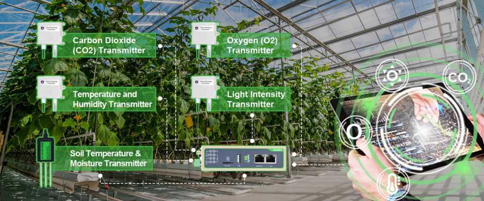
The most famous gadgets for smart agriculture system include weather stations, which combine different smart farming sensors. Their location is usually across the fields where they collect different data from our environment and then send it into the cloud.

Furthermore, the measurements provided are useful in mapping these climate conditions, choosing appropriate crops, as well as taking the necessary measures in improving their capacity, for example in precision farming.

Greenhouse Automation

Farmers usually make use of manual intervention for controlling any greenhouse environment. Using IoT sensors makes it possible to be able to get the best real-time information regarding greenhouse conditions like humidity, soil conditions, temperature, and lighting.

Also, adding to the sourcing of environmental data, the weather stations have the ability to adjust conditions automatically to help in matching the necessary parameters. Greenhouse automation systems usually make use of similar principles.

Growlink and Farmapp are IoT agriculture products which offer some capabilities. Also, GreenIQ is an interesting product which makes use of smart agriculture sensors. Also, it is a well-known smart sprinklers controller, which allows the management of lighting and irrigation systems remotely.

Crop Management

Another type of the IoT product in agriculture, as well as a different precision farming element are the crop management devices. Like the weather stations, you have to place them in a specific field to help in collecting data that is crop framing specific. These include precipitation, temperature, general crop health, and potential of leaf water.

Therefore, you will be able to monitor the crop growth, as well as anomalies that prevent infestations or diseases effectively,which could bring harm to your yield.

Cattle management and monitoring

Similar to crop monitoring, some IoT agriculture sensors exist, which could be attached onto animals present on a specific farm in monitoring their log and health performance. With livestock monitoring and livestock tracking, you will be able to get reliable data on physical location, well-being, and stock health.

For instance, these sensors will be able to locate the sick animals, which will help farmers to separate them from the others to prevent contamination. Making use of drones from the real-time tracking will also assist farmers i9n reducing staffing expenses. Its function is similar to the IoT devices for petcare.

Precision farming

This is also called precision agriculture. It refers to efficiency as well as producing data-driven decisions that are accurate. Furthermore, it is included among the most effective and widely used applications or use case of the IoT in agriculture.

When you make use of IoT sensors, farmers will be able to collect different metrics on every aspect of the fieldโ€™s ecosystem and microclimate. These include humidity, soil condition, temperature, lighting, pest infections, Co2 levels, and humidity. Also, the data allows farmers to get an estimate of the right amounts of pesticides, fertilizers, and water, which is useful for their crops, raise healthier and better crops, as well as reduce the necessary expenses.

For example, CropX helps in building IoT soil sensors, which measures the soil temperature, moisture, as well as electric conductivity. This allows the farmers to consider each of the unique needs of crops.

Agricultural drones

One very promising and well-known AgriTech advancements is the utilization of agricultural drones in our smart farming. This is also called unmanned aerial vehicles (UAVs). These drones are more equipped than the satellites and airplanes in collecting agricultural data.

Asides from their surveillance capabilities, these drones have the ability to carry out different tasks that required the use of human labor previously. These include fighting infections and pests, crop monitoring, agricultural spraying, planting crops, locating shrinking agricultural lands, etc.

Predictive Analytics

Predictive data analytics and precision agriculture work together. While the smart sensor and IoT technology can serve as a goldmine for the real time data, using data analytics assists farmers in making some sense from it, as well as having some important predictions. These include time for crop harvesting, risks of infestations and diseases, yield volume, and more. Also, the tools for data analytics help to ensure farming. This depends inherently on the weather conditions, which are more predictable and manageable.

Management Systems

You can represent a very complex approach to the IoT products used in agriculture by the management systems of farm productivity. Usually, they include some agriculture IoT devices and IoT sensors, which are installed on these premises, coupled with a strong dashboard having analytical capabilities, as well as in-built reporting and accounting features.

Furthermore, this provides capabilities of farm monitoring that allows users to be able to streamline the majority of their business operations.

Asides from the listed use cases of IoT in agriculture, there are some important opportunities, which includes storage management, vehicle tracking, automation, logistics, etc.

What you should Consider Before You Develop a Smart Farming Solution

iot smart farming

Now you can see that the applications of IoT in agriculture are numerous. There are lots of ways through which smart devices will be able to assist you in increasing the revenue and performance of your farm. However, developing agriculture IoT apps is a difficult task.

There are some challenges you must take note of if you wish to get involved in smart farming applying IoT in agriculture.

The brain

The data analytics has to be the center of any smart agriculture solution. This collected data will offer little assistance if you fail to make proper sense of it. Therefore, there is a need to have strong data analytics capabilities, as well as apply some machine learning and predictive algorithms to help in obtaining actionable insights that are based on this collected data.

The hardware

In order to create an effective IoT solution for our agriculture, there is a need to go for device sensors. You can also create a custom sensor. Whatever choice you make depends on the information you wish to collect, as well as your solutionโ€™s purpose generally. Whatever the case is, your sensorโ€™s quality is important to your productโ€™s success. It depends on the accuracy of any data collected, as well as its reliability.

The mobility

The applications of smart farming must be tailored to be used in this field. As a farm manager or business owner, you should have access to the information remotely or on site through a desktop computer or smartphone.

In addition, each of the connected device has to be autonomous, as well as possess the wireless range necessary to be able to communicate with the other devices, as well as send data onto the main and central server.

Connectivity

There is a need for data transmission between the many different agricultural facilities. This is a challenge for smart farming adoption. Today, the IoT devices make use of different connection protocols, though efforts required for developing the unified standards are presently underway. Furthermore, the advent of technologies and 5G space-based internet hopefully, should find a solution to the problem.

Infrastructure

There is a need to have a strong internal infrastructure to make sure that your application for smart farming performs properly as well as ensure it handles the data load properly.

Also, the internal systems must be secure. When you donโ€™t secure the system properly, it once increases the possibility of anyone breaking into it, to steal your data, as well as take control of the autonomous tractors.

Maintenance

Maintaining your hardware could be a major challenge which is very important for the IoT products used in agriculture. This is because the sensors are useful in this field and can get damaged easily. Therefore, ensure that the hardware is easily maintained and is durable. Otherwise, you will end up replacing these sensors too often.

Data Security

IoT technology and precision agriculture implied working with different large data sets. This increases possible security loopholes, which perpetrators could use for hacking attacks and data thefts. For example, many farms make use of drone to transmit data to the farm machinery. The machinery helps in connecting to the web. However, it has very little to no security protection like user passwords.

Some basic security recommendations for IoT in agriculture include the use of encryption methods in protecting sensitive data, monitoring of data traffic, storage of data in blockchain to keep its integrity.

Conclusion

We have explained in detail the applications and uses of IoT in agriculture. We hope more advancements in agriculture result from the use of IoT technology.

Laser Drilling in PCBs: How It Works & Why It Matters

PCB Laser Drilling

Laser drilling enables ultra-precise hole formation in PCBs, creating critical interlayer connections that power todayโ€™s advanced electronics. This technology is essential for manufacturing high-density interconnect (HDI) boards found in modern slim devices like smartphones and wearables. Unlike mechanical drilling, laser systems achieve unmatched accuracyโ€”even at microscopic scalesโ€”ensuring reliability in increasingly miniaturized designs.

The process harnesses concentrated laser energy (from COโ‚‚ or UV sources) to vaporize material with pinpoint precision. As an acronym forย Light Amplification by Stimulated Emission of Radiation, a laserโ€™s coherent beam eliminates physical contact, avoiding mechanical stress and enabling cleaner, smaller holes than traditional drill bits can produce.

What is Circuit Board Drilling?

Circuit board drilling is a fundamental process in PCB manufacturing that involves creating holes in the board substrate. These holes serve various purposes, including:

  1. Mounting components
  2. Creating electrical connections between layers
  3. Facilitating the flow of signals and power

Traditionally, mechanical drilling has been the go-to method for creating these holes. However, as PCB designs become more complex and miniaturized, laser drilling has gained prominence, especially for creating smaller, more precise holes.

Why is Laser Drilling Required for PCB?

YouTube video

Laser drilling has become increasingly essential in PCB manufacturing due to several factors:

1. Miniaturization

As electronic devices become smaller and more powerful, PCBs must accommodate more components in less space. Laser drilling allows for the creation of extremely small holes, enabling higher component density.

2. High-Density Interconnect (HDI) Boards

HDI boards require a large number of small, precise holes to connect multiple layers. Laser drilling is ideal for creating these microvias efficiently.

3. Precision

Laser drilling offers unparalleled accuracy in hole placement and size, which is crucial for advanced PCB designs.

4. Material Compatibility

Lasers can drill through a wide range of PCB materials, including those that are difficult to process with mechanical drills.

5. Non-Contact Process

Unlike mechanical drilling, laser drilling is a non-contact process, reducing the risk of damage to delicate board structures.

Read more about:

How Small of a Hole Can a Laser Drill?

One of the most significant advantages of laser drilling is its ability to create extremely small holes. The size of holes that can be laser-drilled depends on several factors, including:

  • The type of laser used
  • The material being drilled
  • The thickness of the PCB

Typically, laser drilling can create holes as small as 25 microns (0.001 inches) in diameter. Some advanced systems can even produce holes as small as 10 microns. This capability is crucial for creating microvias in HDI boards and enabling the production of increasingly compact electronic devices.

Advantages of Laser Drilling

Laser drilling offers numerous advantages over traditional mechanical drilling methods:

1. Precision and Accuracy

Lasers can create holes with extremely tight tolerances, ensuring consistent size and placement.

2. High-Speed Processing

Laser drilling can be performed at very high speeds, increasing productivity in PCB manufacturing.

3. Flexibility

Laser systems can be quickly reprogrammed to accommodate different hole patterns without changing physical tooling.

4. Reduced Wear and Tear

As a non-contact process, laser drilling eliminates the need for physical drill bits, reducing maintenance and replacement costs.

5. Clean Process

Laser drilling produces less debris and doesn’t require cutting fluids, resulting in a cleaner manufacturing environment.

6. Ability to Drill at Angles

Some laser systems can drill holes at angles, which is difficult or impossible with mechanical drilling.

7. Suitable for Delicate Materials

Laser drilling can process thin and fragile materials without causing damage or delamination.

Different Methods of Laser Drilling

Laser drilling techniques have evolved to meet various manufacturing needs. Here are the primary methods used in PCB production:

1. Single-pulse/Shot Laser Drilling

This method uses a single, high-energy laser pulse to create a hole.

Advantages:

  • Very fast process
  • Suitable for thin materials

Limitations:

  • Limited hole depth
  • May not be suitable for all materials

2. Percussion Laser Drilling

Percussion drilling uses multiple laser pulses to gradually create a hole.

Advantages:

  • Can create deeper holes than single-pulse drilling
  • Offers better control over hole shape

Limitations:

  • Slower than single-pulse drilling
  • May cause more heat-affected zones around the hole

3. Trepanning

Trepanning involves using the laser to cut around the circumference of the desired hole.

Advantages:

  • Can create larger holes with very smooth walls
  • Allows for precise control of hole diameter

Limitations:

  • Slower than other methods for small holes
  • May not be suitable for very small hole sizes

4. Helical Laser Drilling

This method uses a rotating laser beam to create holes in a spiral pattern.

Advantages:

  • Can create deep holes with high aspect ratios
  • Produces very smooth hole walls

Limitations:

  • Requires specialized equipment
  • May be slower for certain applications

Which Lasers are Suitable for Drilling Micro Holes?

Several types of lasers are used for drilling micro holes in PCBs, each with its own strengths:

1. Excimer Lasers

  • Ideal for creating very small, precise holes
  • Commonly used for microvias in HDI boards

2. Solid-State Lasers

  • Include Nd:YAG and fiber lasers
  • Offer good precision and are suitable for a range of materials

3. CO2 Lasers

  • Widely used for drilling in organic PCB materials
  • Cost-effective for many applications

4. Ultrafast Lasers

  • Include femtosecond and picosecond lasers
  • Provide extremely high precision with minimal heat-affected zones

The choice of laser depends on factors such as the PCB material, required hole size, and production volume.

Types of Laser Drilling Machines

Laser drilling machines come in various configurations, each suited to different PCB manufacturing needs:

1. CO2 Lasers

CO2 lasers are widely used in PCB manufacturing due to their versatility and cost-effectiveness.

Advantages:

  • Excellent for drilling organic PCB materials
  • High power output for fast processing
  • Relatively low operating costs

Limitations:

  • Limited in drilling very small holes (typically >75 microns)
  • Not suitable for some metal-based materials

2. Nd:YAG Lasers

Nd:YAG (Neodymium-doped Yttrium Aluminum Garnet) lasers offer high precision for micro-drilling applications.

Advantages:

  • Can drill very small holes (<50 microns)
  • Suitable for a wide range of materials, including metals
  • High peak power for efficient drilling

Limitations:

  • Higher initial cost compared to CO2 lasers
  • May require more maintenance

3. Combination of Nd:YAG and CO2 Laser Processes

Some advanced PCB manufacturing systems combine both Nd:YAG and CO2 lasers to leverage the strengths of each technology.

Advantages:

  • Versatility to handle a wide range of materials and hole sizes
  • Optimized processing for different PCB layers

Limitations:

  • Higher system complexity and cost
  • Requires expertise to manage multiple laser technologies

PCB Laser Drilling vs Mechanical Drilling

While both laser and mechanical drilling have their place in PCB manufacturing, it’s important to understand their differences:

Laser Drilling

Advantages:

  • Can create extremely small holes (down to 10-25 microns)
  • Non-contact process, reducing wear and tear
  • High precision and repeatability
  • Suitable for delicate and thin materials

Limitations:

  • Higher initial equipment cost
  • Limited in creating larger holes efficiently
  • May have issues with certain materials (e.g., some metals)

Mechanical Drilling

Advantages:

  • Cost-effective for larger hole sizes
  • Can drill through multiple board layers efficiently
  • Suitable for a wide range of hole sizes

Limitations:

  • Limited in creating very small holes (<75 microns typically)
  • Tool wear can affect precision over time
  • May cause burrs or rough edges requiring post-processing

The choice between laser and mechanical drilling often depends on the specific requirements of the PCB design, production volume, and available budget.

Facts about PCB Laser Drilling Cost

While laser drilling offers many advantages, cost is an important consideration for manufacturers. Here are some key facts about PCB laser drilling costs:

1. Initial Investment

Laser drilling equipment requires a significant upfront investment, often higher than mechanical drilling systems.

2. Operating Costs

  • Lower consumable costs (no drill bits to replace)
  • Potentially higher energy consumption
  • Specialized maintenance may be required

3. Throughput Considerations

  • Laser drilling can be faster for small holes, potentially reducing per-unit costs
  • For larger holes, mechanical drilling may be more cost-effective

4. Material Costs

Some materials optimized for laser drilling may be more expensive than standard PCB materials.

5. Long-Term Cost Benefits

  • Reduced need for rework due to higher precision
  • Ability to produce more complex boards, potentially increasing product value

6. Scalability

Laser drilling systems can often be scaled more easily to meet increased production demands.

While the initial cost of laser drilling may be higher, it can offer long-term cost benefits, especially for high-volume production of complex PCBs.

Laser-Drilled Microvia-in-Pad Technology in Your HDI PCB

Laser-drilled microvia-in-pad technology is a crucial advancement in High-Density Interconnect (HDI) PCB design. This technique involves creating small, laser-drilled vias directly in the pad of a component, offering several benefits:

1. Increased Routing Density

By placing vias directly in component pads, designers can achieve higher routing density and more efficient use of board space.

2. Improved Signal Integrity

Shorter connection paths reduce signal degradation and improve overall signal integrity.

3. Enhanced Thermal Performance

Microvia-in-pad can improve thermal dissipation, crucial for high-power components.

4. Reduced Board Size

This technology allows for more compact PCB designs, essential for miniaturized electronic devices.

5. Support for Advanced Packaging

Microvia-in-pad is crucial for supporting advanced component packages like Ball Grid Arrays (BGAs) with fine pitches.

Implementation Considerations:

  • Requires precise control of laser drilling parameters
  • May need specialized PCB materials for optimal performance
  • Demands careful attention to plating and filling processes

As electronic devices continue to shrink while increasing in functionality, microvia-in-pad technology enabled by laser drilling will play an increasingly important role in PCB design and manufacturing.

Conclusion

Laser drilling has revolutionized PCB manufacturing, enabling the production of increasingly complex and miniaturized electronic devices. Its ability to create precise, small-diameter holes is crucial for high-density interconnect boards and advanced packaging technologies.

While laser drilling offers numerous advantages in terms of precision, flexibility, and ability to work with delicate materials, it’s important to consider factors such as cost, specific application requirements, and material compatibility when choosing between laser and mechanical drilling methods.

As technology continues to advance, we can expect further innovations in laser drilling techniques and equipment, potentially opening up new possibilities in PCB design and electronics manufacturing. Manufacturers and designers who stay abreast of these developments will be well-positioned to create cutting-edge electronic products that meet the ever-increasing demands of the modern world.

Whether you’re a PCB designer, a manufacturer, or simply someone interested in the intricacies of electronics production, understanding laser drilling technology is key to appreciating the complexity and precision that goes into every electronic device we use in our daily lives.

Exploring the Facts of PCB Printing Services

Amplifier PCB

PCBs (Printed Circuit Boards) are becoming pretty popular in the 21st century. With the demand for smaller, powerful gadgets increasing, manufacturers are turning to PCB to make this devices a reality. Printed Circuit Boards connect each component found inside an electronic gadget, helping it function accordingly. Due to their compactness and versatility, PCBs have become pretty popular in light production companies, electronic companies and so on.

However, even though PCBs are tiny, they are pretty tricky to manufacture as you need to remember tricky factors such as impedance control and copper weight. Therefore, most people turn to PCB manufacturing companies to build their PCBs. But what Printed circuit board printing services can you get out there? And what are the benefits of turning to PCB manufacturers to make your PCB?

PCBs in a Nutshell

PCBs are typically built using bare boards made out of copper. The PCB manufacturer then utilizes high-tech gadgets and other components such as Gerber files to curve the client’s design on the copper board to develop a Printed Circuit Board.

In case the PCB encompass multiple layers, the PCB Manufacturer must then line up the layers and then bind them to attain a secure fit.

The process takes up a lot of time, and PCB manufacturers have to be extra careful to avoid messing up the design handed over to them by the customer. What’s more, it is possible to break down the entire process into multiple stages, each of which is pretty crucial to attaining the end product.

Printed Circuit Board Services

What the Manufacturer needs from you

Gerber Files

Before providing any PCB services, the PCB manufacturer has to request for a Gerber file. These open ASCII files contain details on every Physical PCB layer on your board design be it a hobby design or a complex design. PCB objects, for example, silkscreen images, solder mask, vias, and copper traces, are all well represented using a draw code or a flash. They are then defined using vector coordinates.

After undertaking a file check, manufacturers then utilize these crucial files to translate your PCB design into an actual PCB at an affordable price.

Generating a Gerber file

Generating Gerber files is pretty easy because the only tool you will require will be a PCB designing software. However, the process of developing the actual correct design tends to vary depending on the software you will utilize. What’s more, these files do not have to bear unique names. However, they all have a standard extension, for example, .gbr or .gb.

Once you have made your Gerber file, you can then advance to the next stage.

PCB Fabrication Services

If you are having trouble producing your PCB from scratch, you can easily find a manufacturer online to generate a custom PCB for you. Of course PCB fabrication is not free and you will have to pay some amount of money, but the outcome is worth every penny.

In most cases, the PCB manufacturer will ask you for the following parameters before processing your PCB order:

The Parameters

–          Board type โ€“ The Manufacturer will need to learn details on the board type that you want

–          Size โ€“ Here, you will have to provide the PCB’s maximum length and width. Using this information, the PCB manufacturer will easily figure out the maximum size of your PCB

– Number of PCB being produced โ€“ here, specify whether you want a single board or if you want your PCBs produced in batch production form.

–          Layers โ€“ You specify the number of layers the PCB will have. For example, if you want your PCB to bear one layer, then you can simply request for a one layer PCB.

–          Base Material โ€“ Here, specify the type of base material that you want your Manufacturer to utilize. For example, you can opt to work with aluminum or rogers. Some companies will also ask whether you want a metal core or a plastic core.

–          Board Thickness โ€“ Specify the parameters that describe the printed circuit board thickness. Using this information the PCB manufacturing company will figure out the right copper weight to use.

–          Min spacing/track โ€“ Here, you must clearly state the minimum track spacing. Using this information, the manufacturer can figure out the trace width to utilize.

–          Min hole size โ€“ Specify the minimum hole size to help the Manufacturer during the drilling process.

–          Solder mask โ€“ Here, provide details regarding the type of solder mask that you want to be utilized on your PCB

–          Silkscreen โ€“ silkscreen comes in two varieties, white and black. You can opt for either of the two. Or you can choose to utilize your Printed circuit board without a silkscreen.

–          Surface finish โ€“ choose the surface finish that you want your Manufacturer to utilize on your PCB.

Other Details that might come in Handy

You can also opt for a lead or a lead free PCB. Doing so helps your PCB manufacturer known the type of solder paste to use on your circuit boards and the lead time needed to produce your PCB.

A Gerber file should also accompany all these details to help the Manufacturer get your design right in the PCB fabrication process.

Using these details, a PCB manufacturing companies such as PCB partner can easily print out your PCB order using high-tech machines with remarkable precision. However, you should always double check on the Manufacturer’s experience before handing out the contract. Doing so will ensure that you get a high-quality finished product in return while avoiding hidden costs and scam companies. You can also contact the PCB manufacturing company via a message or through a phone call. Using this methods, you can easily discuss critical issues such as the price of developing your PCB and how long it will take to receive your board.

Exclusive Services

Some companies will offer exclusive services which feature special requirements meant to make more advanced circuits and more efficient PCBs. These exclusive solution, however, do not come at a low cost, therefore be keen when making such an order.

Other services offered for the Printing of Printed Circuit Boards

PCB Drilling

The PCB drilling process tends to be the most tiresome, time-consuming, and expensive phase of the PCB manufacturing process. That is because PCB manufacturers have to carry out this stage carefully to ensure that they develop a high-quality PCB.

The PCB holes can be generated via electrochemical etching or via punching, laser cutting, or drilling. However, most PCB manufacturers tend to favor a combination of electrochemical etching and chemical milling to carry out this process.

Solder mask PCB Assembly and Printing

After Printed Circuit Board Fabrication, the traces of copper left on the PCB are prone to corrosion and oxidation due to exposure to the environment. The best way to shield your PCB against these issues and boost its durability is by placing a protective layer on the PCB known as a solder mask layer.

Solder Mask

A solder mask is a pretty thin layer made out of polymer. Manufacturers utilize this layer to help shield a PCB from:

–          Short circuit

–          Oxidation

–          Environment influences

–          Dust et cetera

A solder mask is pretty crucial in terms of helping boost the durability of a PCB. However, the solder masking process can be pretty tricky to carry out. But the good thing is that you can easily find a PCB manufacturer to carry out this process.

Types of Solder Mask Services Offered

There are several solder mask services offered in the PCB market today. These services include:

–          Bottom and top side masks โ€“ These solder masks are utilized mainly by engineers to help them identify various openings on a Print Circuit Board.

–          Epoxy liquid โ€“ If you are looking for an affordable solder mask, then this should be your first option. Epoxy is an excellent polymer, and it offers great protection to your PCB at a reasonable cost.

–          Liquid photoimageable โ€“ LPI or photoimageable is a solder mask that is a mixture of two different liquids. The liquids used to make this solder mask are stored separately and are only mixed right before they are applied to the PCB to ensure longer shelf life.

–          Dry film photoimageable โ€“ Dry film photoimageable is a solder mask that best suits high-density wiring Printed Circuit Boards. That is because these solder masks do not flood the prior put through-holes. It is hence pretty efficient.

Surface Finish

PCB Manufacturing with Immersion Gold-ENIG Surface Finish

In most cases, the solder mask utilized on a PCB tends to leave behind exposed copper areas on the PCB. These areas have to be plated using a suitable surface finish so as to lower the chances of oxidation. PCB manufacturers worldwide are now offering surface finish services to help clients cope with this issue easily.

Also under this category, some manufacturers are now offering copper plating service. These services help boost the thickness of a PCB making it more rigid and efficient.

Surface Treatment PCB Assembly Services

Printed Circuit Board surface treatment refers to the crucial process of creating a surface layer on a PCB artificially. The reason why this process is vital is that it helps to boost the electrical and soldering properties of a PCB.

Many surface treatment services exist. Here are some common surface treatment services that you can find:

Hot air Solder Leveling or HASL

HASL is a simple process whereby a PCB manufacturer coats your PCB using molten tin-lead solder. They then flatten the molten tin lead using heated compressed air to form a layer resistant to copper oxidation. Moreover, this layer is resistant to copper oxidation, making a PCB more efficient and durable.

During this process, the following parameters have to be mastered:

–          Lifting speed

–          Dip soldering time

–          Air knife pressure

–          Air knife air temperature

–          Welding temperature

Organic Protective film or OSP

OSP or organic protective film works by spraying organic chemicals on a Printed Circuit Board to provide a protective layer. An OSP layer has to bear the following characteristics for it to work:

–          It should be shock resistant

–          It should have oxidation resistance properties

–          And lastly, it should have moisture resistance properties

Immersion Silver

Typically silver bears stable chemical properties. Therefore, Printed Circuit Boards that have undergone the immersion silver process tend to have excellent electrical properties even when exposed to pollution, humidity, and heat.

Immersion tin

After inserting organic additive into a tin immersion solution, the layer of tin that comes out of this mixture tends to overcome common issues caused by tin and tin whisker migration. With these issues out of the way, the circuit board tends to have better solderability and thermal stability.

Conclusion

Printed Circuit Boards have become a primary component of the 21st century. Almost every gadget you come across now bears a PCB, be it a computer, a street light, or even a flashlight. But, even though these components are crucial, manufacturing them can be challenging for many people. However, with the emergence of multiple companies bearing skilled engineers willing to manufacture Printed Circuit Boards for various clients, this issue is starting to become extinct. Therefore, if you want to print a PCB or add new features to your PCB but do not have the equipment to do so, remember that you can easily find a manufacturer to help you out even though it won’t be for free.

Top 10 Digital IC design Companies in China

Digital IC

Are you looking for a job in the digital IC design industry? Do you know how to find companies that design ICs in China? If you’re an engineer, designer, entrepreneur or investor in the semiconductor industry, this post will interest you.

What is digital IC design?

A proper digital IC design begins with a specification of the desired function. The specification can come from an outside source, or the manufacturer can provide it. Then the specification is translated into a Verilog or VHDL netlist, then verified against the specifications. Finally, there is synthesis of the netlist to produce a physical layout. Gate layouts are usually available from the IC manufacturer’s libraries.

Those working on the design process translate the specifications into digital blocks and logic circuits. The process is procedural, but many constraints associate with this type of IC. The design process is a combination of technological constraints and foundry processes. These factors result in several possible designs.

Why is digital IC design is important?

Creating a digital Integrated Circuit (IC) involves translating a set of determinations into computerized blocks assembled into basic circuits. The development of advanced IC plans, including the design of a foundry cycle, involves the advancement of frameworks and cycles. Creating a digital IC is not as simple as creating a conventional one; it requires extensive education and specialized training.

Digital designers can use libraries provided by IC manufacturers, which contain information on gate delay and layout.

Current Status of IC Industry in China

In February 2021, prediction aligned China’s IC industry to meet 70% of the domestic demand. Homegrown silicon was integral in meeting the demand, but in February, US sanctions began to bite. Meanwhile, China’s production remained below global standards and faced an increasing capacity gap.

In terms of volume, semiconductor demand in China was USD155 billion, with about 38% coming from non-Chinese companies. The largest demand came from four major Chinese smartphone companies and a non-China ICT company. Overall, China’s IC industry generated USD23.7 billion in local manufacturing, which was only 23.7 percent of the global demand. In contrast, China’s local IC manufactured industry produced only USD23.7 billion the previous year.

Vimicro Corporation

The Vimicro Corporation is a technology company founded in Beijing, China, in 1999. Its founders, who came from Silicon Valley, received support from the Ministry of Information Industry in establishing the company. Vimicro is dedicated to developing advanced mixed-signal multimedia chips and has several products currently available for domestic and international markets. Vimicro’s products target several fast-growing application fields.

Vimicro Corporation is a leading fabless chip company based in Beijing. Vimicro develops mixed signal multimedia chips, including video processors and networked video applications. It is the first Chinese chip design company with proprietary technology listed on Nasdaq. As one of the most influential and innovative chip companies in China, Vimicro has a strong market presence in the region and already incorporated into several Chinese companies.

Its patent portfolio spans over 2094 patents worldwide, belonging to 15 unique patent families. Of these, 687 are active and have received 73 citations. The company’s recent AI processor is for low power consumption and super-fast processing. It was also recently teamed up with the Ministry of Public Security to draft part of a national standard on video surveillance, which can help crack crimes. China has one of the world’s largest video surveillance networks and will be able to benefit from this development.

Its business

While a company’s performance does not necessarily reflect the future, many factors could affect its growth in China. These factors include the company’s ability to attract and retain employees. The company also faces several risks related to its business, including currency fluctuations. While investors should monitor the risks associated with investing in the company, these factors do not necessarily indicate that Vimicro is not likely to grow. While this situation is somewhat unlikely, management expects that its business in China will continue to grow in the coming years.

The Vimicro Corporation products target the rapidly growing markets of video surveillance, broadcast TV, gaming, and digital signage. With two decades of history, Vimicro is a company to watch in China.

Jingjia Micro

Jingjia Micro

Jingjia Micro’s latest GPU is called the JM7200. The new chip is a 28nm version of the company’s previous GPU, which was robust enough for military aircraft displays. It is compatible with OpenCL 2.0 and OpenGL 4.5 APIs. It will not compete directly with the best-selling AMD and NVIDIA GPUs, but it will be able to take on both companies in the data center and cloud computing segment.

Jingjia Micro, a military-civilian integrated company focusing on graphics processing, made the latest GPU. The company developed China’s first homegrown GPU, the JM5400, and is now promoting it outside the military sector. Its latest chip is about the same speed as the GeForce GTX 1080, so it is capable of boosting gaming performance.

Jingjia Micro’s upcoming GPU could match AMD’s Radeon RX 560 or GeForce GTX 1080

Jingjia Micro has been waiting for the right moment to release its first marketable GPU for years. The company recently dropped its first domestically produced GPU, the JM9231. The company’s upcoming GPU is comparable to the GeForce GTX 1080 or Radeon RX 560 in terms of performance and power consumption. Jingjia Micro’s upcoming GPU contains a TDP of only 150W, similar to GeForce GTX 1080 or Radeon RX 560.

Besides, the company’s upcoming GPU could match the prices of GeForce GTX 1080 and Radeon RX 560. Besides, the upcoming GPU from Jingjia Micro could match the price tag of AMD’s Radeon RX 560. Although Lao Huang’s claims may seem overly optimistic, it’s a good sign. The company is planning to launch two graphics cards. The entry-level JM9231 will be competitive with AMD Radeon RX 560 or GeForce GTX 1080. The JM9271 is more powerful and could even match GeForce GTX 1080 or GeForce GTX Vega 64.

Jingjia Micro’s non-public offering of stocks

The company plans to use the funds raised from the stock sale to invest in consumer electronics, high-performance graphics processor chips, and general-purpose chips. The fundraising effort aims to further strategic planning in IC design for the consumer electronics sector. Sino IC Capital Management will manage the China Integrated Circuit Industry Investment Fund. The raising of the funds will happen through the Hunan High-Tech Venture Capital Investment Group, a government-backed investment platform that aims to foster strategic emerging industries.

Goke Microelectronics

The Goke Microelectronics Company is a Chinese IC design firm. This company provides professional services and develops chips for satellite, digital cable, wireless communication, and DTMB. Its product line includes a H.265 HD video chip, modern solid storage controlling chip, Wi-Fi, and an NDS advanced security decoding chip.

Integrated circuit design enterprise

Founded in 2008, Goke Microelectronics Co., Ltd. is a leading provider of multimedia chip solutions in China. Its core technologies include intelligent 4K decoding chip, H.264/H.265 HD security chip, high-end solid-state memory master control chip, and Beidou navigation and positioning chip, which has independent intellectual property rights.

Government subsidies received

GOKE MICROELECTRONICS, a semiconductor manufacturer, received nearly $100 million in government subsidies in 2018 and another $24 million in 2017. These amounts are the total government subsidy amounts the firm received during the calendar year. You calculate the amount of subsidies received using the year-average exchange rate of the Chinese Yuan. GOKE may have also received other types of state aid.

Risk of being included in the Entity List

Currently, the Chinese company is part of the Entity List for Semiconductors, Chips, and Advanced Electronics. Its main product lines include microprocessors, flash memory, and integrated circuits for artificial intelligence and quantum computing. Goke has headquarters in Changsha, central Hunan province. One of its subsidiaries, New H3C, is an independent semiconductor, information technology, and financial company.

Giantec Semiconductor Company

The primary focus of Giantec Semiconductor Corporation is providing integrated circuit products and services to customers worldwide. The company offers products for diverse industries including electronics, telecommunication, smart energy meters, medical and transportation. All its products meet or exceed the international standards and are marketed to customers worldwide.

A semiconductor company headquartered in Shanghai, Giantec Semiconductor is one of the largest suppliers of EEPROM chips. These chips are useful in storing configuration parameters in smart devices, personal computers, and other tools of the digital age. The company accounted for over 80% of its operating income in the first half of 2019.

The company is part of a larger industry and has an impressive customer base in Asia. Its automotive business has helped it establish a strong presence in China, a major EEPROM market. Its products include two-wire serial EEPROMs, application-specific ICs, and smart cards. It also manufactures signal chain-operation amplifiers, automotive parts, and VCN drivers.

Gross profit margin

Founded just a decade ago, the Shanghai-based semiconductor giant Giantec Semiconductor Corporation (GSIC) is a leading supplier of EEPROM chips. In the first half of 2019, EEPROM chips accounted for 88.4% of the firm’s operating income. However, this profit-generating company faces several challenges.

The company’s prospectus indicates that the gross profit margin for EEPROM production has been around 50% since 2016. Meanwhile, the gross profit margin for smart card chips has hovered between 24% and 28%. It is hard to ignore the potential of this kind of relationship. For this reason, Giantec is one of the most profitable companies in the semiconductor industry. Despite its small size, it has managed to earn a huge profit.

Product lines

Based in Shanghai, Giantec Semiconductor Company in the country has four distinct product lines. It specializes in EEPROM chips. It has received ISO9001 and ISO14001 certifications and is one of the qualified suppliers of the Ministry of Housing. The company’s products are in a wide range of consumer electronics, industrial, and medical products.

The company offers its entire EEPROM and MCU smart card solutions to customers worldwide. The company’s specialized technology allows it to meet clients’ needs across various industries. For example, it can provide epitaxial, 4-inch, 6-inch, or eight-inch silicon-on-insulator (SOI) wafers. The company has a full range of product lines for various applications, including medical devices, and is developing a Power Management line.

Major supply chain upstream

On November 26, Giantec received a green light from China’s financial regulator to list its shares on the Shanghai Stock Exchange Sci-Tech Innovation Board, otherwise known as the Star Market. The company’s operating income accounted for 88.4% of its revenue in the first half of 2019.

The major supply chain upstream for Giantec Semi-Conductor Company has headquarters in Shenzhen, China. This region is home to several companies that manufacture electronic components. The company has a significant presence in the world market and operates in Shenzhen, Hong Kong, and Taiwan.

Dosilicon Company

Dosilicon Co., Ltd. is a fabless semiconductor company specializing in designing and manufacturing small and medium general-purpose memory chips. It has headquarters in Shanghai City. The company’s products range from DRAM memory to NOR flash memory and MCP, but it’s also one of the few domestic semiconductor companies with multiple design processes. This information service combines company, industry, and country data to give investors an overall picture of the industry.

Its product portfolio includes various types of memory chips, semiconductors and electronic components. The company has significantly improved its main products by continuously investing in R&D capabilities and technology accumulation. With its multi-product line layout, it is achieving significant returns in the market. It has also established a stable supply chain system. The company’s products are widely useful in smart watches, optical cats and 5G communication. While the semiconductor industry is booming, Dongxin Semiconductor Co., Ltd. is still a relatively new player.

Founded in 2014, Dosilicon Co., Ltd. designs, manufactures, and sells memory chips worldwide. The company offers NAND flash, NOR flash, dynamic random-access memory chips, and multiple chip packages. Its products are useful in many sectors, including mobile phones, industrial control, communication networks, and security. As a result, Dosilicon is a highly competitive semiconductor company. The company is expanding its operations in China and overseas to keep up with the demand for flash memory.

NAND Flash /NOR Flash /DRAM

Dosilicon focuses on NAND flash, NOR and DRAM memory chips for multiple industries. These semiconductors can be useful in various applications including computer memory, mobile phones, and storage devices. The company also offers a variety of design processes, such as DRAM, NOR flash, and MCP (Memory Core Processors).

NOR flash is a memory type with higher read and write performance than NAND storage. The former is better for low-volume storage and high-speed reads. It is also faster than the latter and is primarily useful in consumer electronics. However, it is limited in storage capacity. Neither memory is ideal for all applications, and each has its own disadvantages.

Innosilicon Technology Ltd

Innosilicon

Innosilicon started as an ASIC maker, but expanded into crypto mining in the early 2010s. Today, the company offers a variety of IP solutions and has invested heavily in advanced production nodes at China’s SMIC foundries. The company has also teamed up with GPU developer Xiandong to develop a high-performance server GPU called the Fenghua 1. This GPU rivals the latest models from Nvidia and AMD.

Innosilicon is a leading IP design company

Innosilicon is a one-stop-shop for high-speed mixed-signal IPs. They support a wide range of processes from 130nm to 5nm, and have built a 5nm process library, which is unrivaled worldwide. Moreover, they offer design-to-tapeout services. Their IPs cover the whole DDR process life cycle from prototyping to manufacturing.

Founded in 1998, Innosilicon is one of the world’s leading IP vendors. With over 16 years of experience, they have licensed over six billion high-performance Socs to leading manufacturers. They are official partners of TSMC and SAMSUNG, and have delivered a broad range of 5nm IP. Moreover, their IP has a great price-performance ratio.

Its GPUs are compatible with Linux, Android and Windows

Innosilicon has unveiled a new 4K high-definition desktop graphics card, the Fantasy One. It supports Windows, Linux, Android, and the OpenGL and Vulkan graphics APIs. The company plans to use this GPU in data centers and for VR and AR applications. The GPU is also compatible with the mainstream graphics frameworks such as DirectX.

Innosilicon manufactures standalone graphics cards, which use GDDR6X memory and are compatible with Linux, Android and Windows. The company has already launched its CPUs and is now developing a GPU for the market. The Fenghua No.1 GPU is intended for servers and can support DirectX and OpenGL graphics.

Its GPUs coming soon

Innosilicon is currently prepping its next-generation Fantasy One series. These GPUs will support up to 32 users for cloud-based services, and ship with 16GB of GDDR6X memory. They will support DX11 and DX12 and run up to 64 1080p/60 FPS games simultaneously.

The new GPUs will offer more than 1 trillion transistors and aim at cloud computing, virtual reality, and enterprise applications. Innosilicon will introduce the Fantasy 2 series in 2022, and the company says that this version will be faster and more powerful than the previous generation’s Fantasy One design. However, the company has not yet released any reviews of the new graphics cards, so there are no details on their price and availability.

Phytium Technology Ltd

Whether in the technology industry or not, you’ve probably heard of the Phytium Technology Company in China. You’ll also get an insider’s look at what they’ve been up to. Here, you’ll get to know what makes them unique and their latest technology.

The Phytium Technology Company in Tianjin, a city 70 miles from Beijing, has made news in recent months, when President Xi Jinping visited the company’s headquarters. Phytium is a leading Chinese microprocessor supplier and claims to have the largest market share for these chips. The company has won the support of the Chinese military and has been a shareholder for several years. Founded in August 2014, the company is a joint venture between the Tianjin municipal government and the China Electronics Corp. (CEC).

Phytium is making its chips for personal computers and commercial servers using mature 28 nanometer TSMC processes. Unlike the newest 16 nanometer FinFET processes, designing the company’s chips aims to increase transistor density and shrink die sizes. The company focuses on improving yields and achieving volume production of its Earth and Mars chips. The company is looking for other partners and potential acquisitions.

Phytium’s chips

Phytium Technology Ltd. is a company cited in a Washington Post investigation as a supplier of semiconductor chips for a Chinese supercomputer. These chips would have been useful in the supercomputers used by the Chinese military to test hypersonic vehicles. Despite the company’s ostensible civilian nature, it has ties to the PRC military, including the China Aerodynamics Research and Development Center.

Phytium’s supercomputer

The Chinese military has been building a supercomputer to test hypersonic aircraft, and one of the companies that makes those chips is Phytium. While it is not clear how the military plans to use the new computer, US officials worried that China would keep up with its growing national security and modern weapons capabilities. Phytium is a semiconductor company building supercomputers for military applications for decades. The Chinese government has been a key customer of companies like Cadence and Synopsys.

Chengdu Shenwei Technology Company

Chengdu Shenwei is the second fastest supercomputer in the world. It uses a mix of chips from Intel and Sunway BlueLight, and employs an alpha 64 bit RSIC architecture. The company also claims it has the lowest total cost of ownership of any supercomputer globally. It is also located in a highly innovative part of the city, and is currently testing a variety of hi-tech industries.

Shenwei is the world’s second fastest supercomputer

Chinese researchers and companies developed the second fastest supercomputer in the world. This supercomputer, developed by the Chengdu Shenwei Technology Company, runs on a chip that was first developed by the company 15 years ago. The chip, known as the Sunway TaihuLight, can run at 93 petaflops on sustained workloads and up to 125.4 petaflops on peak workloads.

It uses Sunway BlueLight MPP as its main processor

The new supercomputer installed at China’s National Supercomputer Center in Jinan, which is about three times the size of the previous world record, has a power of 1,000 trillion calculations per second. It will probably rank among the top twenty fastest computers in the world. You can note 8,700 ShenWei SW1600 microprocessors, each designed and produced by a computer institute in Shanghai.

It uses alpha 64 bit RSIC architecture

Alpha is a 64-bit RISC microprocessor. Its development arose from an earlier, failed RISC project. Digital had been planning to replace their VAX line with PRISM, but executives did not see the need to replace it because it was incompatible with the older VMS operating system. Besides, the company would have to wait a long time to release a full software suite before introducing a new processor. Meanwhile, other RISC architectures offered better price/performance ratios.

It uses 260 cores

The Shenwei sw26010 processor has 260 cores and runs at a frequency of 1.45 gigahertz. The processor consists of four computing, management, and memory controller units. Its silicon features three teraflops of performance, which puts it on par with Intel’s “Knights Landing” processor. The Sunway Taihu Light, which costs over 1.8 billion dollars to build, is one of the largest supercomputers in the world.

Shanghai Anlu

Before deciding whether to invest in Shanghai Anlu Information Technology Co. Ltd in China, you should first learn about the company’s founders, products, gross profit margin, and competitors. Then, you can evaluate its overall value based on these factors. After reading the information in this article, you can determine whether it is a good investment. We will also discuss how the company’s management team has performed and whether it is profitable or not.

Founded in 2011, Shanghai Anlu Information Technology Co., Ltd. specializes in producing programmable logic devices and system-on-chips. In addition to providing FPGA products, the company also provides dedicated EDA software for design engineers. Its products aim at industries such as display, communication, industrial control, and artificial intelligence. Their products are useful in various electronic devices and applications, including mobile devices. They’ve been in business for 11 years, and they’ve developed a great number of successful products.

The company has experienced explosive growth in its products in the last few years, especially FPGA chips. The company’s products are currently useful in mobile phones, smart home systems, and other industries. These chips help it enter the supply chain of benchmark enterprises, including Intel, Qualcomm, and Samsung.

Gross profit margin

While its revenue and profit has grown, the gross-profit margin of Shanghai Anlu Information Technology Co-Ltd has remained at the bottom of its peer group for the past three years. In 2018, it fell short of its peer group average by about 20 percentage points. Its blood loss exceeded 80 million yuan. Despite the positive impact of its growth, the company faces numerous challenges in maintaining its profitability.

It is important to note that gross profit margin is an overestimation of revenue. Listed companies have to consider in-price tax and bad-debt loss as important components of revenue, which can greatly affect gross profit margin. We use the “return model” to calculate the profit margin of Shanghai Anlu Information Technology Co. Ltd in China. While it is possible to calculate the gross profit margin of this company using the existing theory, its resulting figure becomes significantly overstated.

Gowin Semiconductor Corporation

GOWIN Semiconductor Corp., founded in January 2014, has grown rapidly since launching its first products. In addition to its products, Gowin also provides software and reference designs for developing FPGAs. The company has headquarters in Guangzhou, China. The company also serves customers worldwide, including in India.

A Chinese FPGA chip developer, Gowin Semiconductor Corp, has completed a heavy B+ financing round to accelerate its localization strategy. The firm primarily provides field-programmable gate arrays (FPGAs), reprogrammable after manufacturing. This type of technology is perfect for a variety of industries. It also targets the Indian market, which may reach $63 billion by 2026.

The National Integrated Circuit Industry Investment Fund led the financing round, the Xiaomi Industry Investment Fund, and the China Merchants Telecom Fund. Other investors included Wentai Technology and Chuanyin Holdings, two private equity firms in China. The company also plans to pay more attention to providing comprehensive and daily information. Many of its shareholders are large domestic semiconductor manufacturers, which may lead to further development of their products.

Company has begun mass production of its low- and mid-density FPGA chips

The Chinese semiconductor company Gowin Semiconductor Corporation has begun the mass production of its low and mid-dense FPGA chips in China. Its chips, designed for embedded use in mobile devices, compete with existing low and mid-density FPGA chips. The company has full intellectual property rights over its chips, configuration can happen after manufacturing. Gowin’s FPGA chips can be useful in various industries, including automotive, telecommunications, and defence. The company is currently concentrating on the mainland Chinese market, where it has received its first order for 10 chips.

Company has filed 22 patents

GOWIN Semiconductor Corporation has announced the release of an mSoC FPGA with an integrated Bluetooth 5.0 Low Energy radio. GOWIN is a global leader in designing and manufacturing semiconductor devices for diverse markets. The company has offices in several countries and R&D centers worldwide. With a strong focus on advancing the semiconductor industry, GOWIN has established itself as a top tier semiconductor partner.

The company’s IP portfolio includes general-purpose SPDIF receiver controllers, BMC encoding solutions, and USB 2.0 interfacing solutions. You can apply the company’s IP to all FPGA products regardless of manufacturer. In addition, Gowin SPDIF receiver IP includes functions such as BMC decode, SPDIF phase detect, and IDDR modules. The IP also allows for flexibility in product development, allowing a wide range of users to take advantage of its IP.

Since the recent ban on foreign semiconductors, Gowin has gained increased attention from investors and clients domestically. China’s Made in China 2025 industrial master plan aims to decrease the reliance on foreign tech companies.

The Different Applications of the Factory Robot Arm

Factory Robot Arm

Factory or industrial robotic arms have become a primary need for most manufacturers who want to stay competitive in the modern market. These robots are in use in many industries, from the automotive to the medical industry. By using these robotic arms, manufacturers from all over the world can automate the services that they offer hence increasing throughput while at the same time lowering labor costs. Moreover, by utilizing robotic arms, manufacturers can enhance workplace safety by assigning dangerous jobs, for example, spray painting cars, to industrial robots. However, all these advantages only scratch the surface regarding how life-changing industrial robots have been to humans. So, how have industrial robot arms changed the life of humans? And how have automated systems affected the manufacturing industry?

Industrial Robot Arms in a Nutshell

Engineers describe robotic arms, which are sometimes simply called industrial robots, as mechanical arms.

Robotic arms have several joints that can rotate in a specific direction or along a particular axis. In addition, most robotic arms tend to be anthropomorphic, which means they try to mimic the movement of a human arm.

Robotic arms are primarily designed to be programmable, and one can program them to undertake various tasks, which include:

  • Manufacturing operations
  • Fabrication
  • Assembly applications

Industrial robotic arms come in varying sizes. They can be tiny gadgets that undertake detailed, intricate tasks, or they can be massive gadgets that undertake strenuous tasks, for example, building houses.

The Origin of Industrial Robotic Arms

ROBOT Manufacturing

Industrial robots were initially built to boost mass production factories and help them produce more goods while incurring lower labor costs. They were also constructed to help lower workplace injuries by assigning dangerous tasks to the bots instead of human workers. Moreover, since industrial robots could undertake monotonous tasks pretty nicely, they free human workers from these strenuous tasks, helping them focus on more critical tasks. As a result, industries like the automotive industry highly benefited from these robots, and their profits started to skyrocket.

These earliest known industrial robot, the unimate, was mainly useful in undertaking simple and repetitive tasks, such as welding. However, robot manufacturing companies have made recent advancements in technology, in particular the invention of robotic sensor and vision technology, has seen robotic arms gaining more applications in the manufacturing industry.

In the 21st century, thanks to gadgets such as high-resolution cameras, GPUs, AI tech, and powerful CPUs, industrial robots bear the intelligence and sense required to undertake new tasks. These vision-augmented, intelligent robots can easily detect obstacles in their environment, identify them by type and even manipulate them.

Through these capabilities, modern robots can now operate more consistently and more accurately. What’s more, these capabilities also increase the number of tasks that can be assigned to robotic arms, making them more efficient.

Component of an Industrial Robotic Arm

Robotic arms are aptly called so since they tend to resemble the arm of a human. These bots are mounted onto a unique base that supports them as they undertake various tasks.

Industrial robotic arms bear several joints that function as axes and help the bot in terms of executing specific movements. The more rotary joints a bot arm bears, the more movements the robot can pull off. Most industrial bot arms have four to six rotary joints.

Other than joints, industrial robotic arms also bear other components that include:

  • Actuators
  • End-of-arm tool
  • Robot controller
  • Sensors
  • Vision systems
  • Power Systems
  • Software components

Types of Industrial Robotic Arms

Different robotic arms exist, however, most of these arms tend to have similar applications even though they bear unique features in terms of how they are built.

The most common types of robotic arms include:

Articulated Robots

Articulated arm bots are simply general purpose bot arms that bear five or more rotary joints. Engineers utilize this term to refer to many other robot arm types for example, a six axis bot is simply an articulated bot arm bearing six degrees of freedom.

Six-axis Bots

These are the most common bots in the manufacturing industry today. They are general purpose and they tend to be pretty flexible.

Collaborative Robots

These are robot arms purposefully designed to undertake hybrid tasks. They work great with human hence their name.

SCARA Robot Arms

These are selectively compliant bots. That means that, when compared to articulated bots, SCARA bots have lower flexibility.

Cartesian Robots or Gantry Robots

These are pretty rigid robot arms that move along a 3 dimensional coordinate plane. These bots typically bear three linear actuators which helps them move a long a 3 dimensional coordinate plane.

Delta Robots

The delta robot(s) are high-speed robotic arms that can carry out tasks requiring great speed and precision.

Cylindrical Robots

Cylindrical robots are compact industrial robot arms that are utilized to undertake simple and small task.

Industrial Applications of Industrial Robotic arms

FULL PCB MANUFACTURING Quote

Robotic arms are popular primarily because they are versatile and can support multiple applications. These bots can support simple applications and can also be utilized to undertake tasks under pretty harsh conditions, making them useful in so many factories.

Automating various tasks saves humans from undertaking highly monotonous tasks and helps them focus on high-value tasks, such as interacting with customers.

Here are the most common applications of a robotic arm in the 21st century:

Palletizing

Manufacturers are now utilizing robotic arms to automate the highly repetitive task of placing products or goods onto pallets.

The use of manufacturing robots to undertake palletizing tasks has made the process more accurate, predictable, and cost-effective.

What’s more, since palletizing is highly repetitive, it poses a threat to the health of human workers. Therefore, utilizing both arms to undertake this task has, without a doubt, boosted workplace safety immensely.

Material Handling

Industrial robotic arms designed for material handling help keep warehouses safer and more efficient. They do so by making sure that materials and goods are:

  • Stored properly
  • Stored in a way that one can easily find them
  • Transported correctly

Automating this process helps accelerate goods delivery to customers while at the same time preventing workplace accidents and improving the efficiency of the facility.

Welding

Advanced industrial factories, for example, automotive factories, utilize industrial robotic arms to undertake welding tasks. That is because these tasks tend to be dangerous and highly repetitive. Hence using bots boosts workplace safety.

What’s more, the welding process tends to substantially impact a product’s quality. Therefore, great precision and accuracy are required when undertaking this task, making robotic arms great candidates for this job.

Inspection

Quality inspection tends to occur at the very end of the production line process. During this production phase, products are inspected to ensure that they meet all the set standards. Therefore, the output of this phase should be viable products of high quality that meet the specified requirements.

If anything goes wrong at this stage, then customers might get products that do not function accordingly, which could tarnish a company’s name for good. Therefore, manufacturers tend to take this phase pretty seriously.

With the development of robotic arms that bear AI and vision systems, companies can now enjoy high-quality real-time inspections. What’s more, the efficiency of the bot arms is high as they can undertake this task 24/7 with great precision, helping reduce downtime and waste.

Pick and Place

Industrial robotic arms that undertake pick and place tasks are typically utilized in modern-day logistics and manufacturing. These bots feature advanced machine vision systems that help them identify various objects, grasp them and then relocate them to a specific, predefined location.

Industrial robotic arms undertake this task quickly and with precision, making the process more efficient. Moreover, their high speed and precision increase the throughput of a company immensely, which ultimately translates to more profits.

Industries that highly utilize the Industrial Robotic Arm

Here are some key sectors that highly use industrial robotic arms to automate their manufacturing processes:

The Automotive Industry

The car manufacturing industry stands at the very top of the list in terms of the sectors that have benefitted from manufacturing robots.

For more than fifty years, the automotive industry has highly relied on industrial robotic arms to carry out assembly line tasks and product quality testing.

By utilizing robot arms alongside humans, manufacturers in this industry can optimize their production process while lowering labor costs and workplace injuries.

Robots in manufacturing industries are versatile and flexible and do not require rest to undertake tasks efficiently. Therefore, manufacturers in this industry primarily utilize them to carry out monotonous tasks.

The Electronics Manufacturing Industry

The demand for smartphones, flat-screen TVs, smartwatches, and other high-tech compact electronics goes up each day. By using the human workforce alone, manufacturers in electronic industries could have difficulty trying to supply goods to satisfy the current demand for these products. However, using high-tech industrial robotic arms, manufacturers easily mass produce high-tech, high-quality compact gadgets using less time and fewer human workers. In doing so, they can deliver high-quality devices to customers at affordable prices.

Moreover, since robotic arms maintain their precision and accuracy throughout the production phase, manufacturers rarely have to deal with defects.

The Food Manufacturing Industry

Robotic arms utilized in the manufacturing process of beverages and foods help manufacturers improve the quality of their products by easily detecting defects using:

  • Sensors
  • Machine vision
  • Processing hardware
  • Processing software algorithms

By using robotic arms in this industry, manufacturers consistently produce high-quality products. In doing so, they maintain their customer base and keep their profit growing in a consistent manner. Moreover, manufacturers in the food manufacturing industry utilizing bot arms in their manufacturing process also report improved customer safety. That is because only high-quality products get past the production line process and onto the hands of the customer.

The Agriculture Industry

Individuals in the agriculture industry utilize industrial robot arms to boost their productivity while at the same time lowering labor costs. For example, farmers can now automate operations such as weed removal, spraying, and pruning using industrial bot arms, reducing labor costs.

The medical Industry

The medical industry has highly benefited from the various advancements in robotic arm technology. Through these advancements, industrial robotic arms can now help surgeons perform critical surgeries require precision.

When working without robotic arms, surgeons face significant challenges regarding precision. Many things can affect their precision, including their own heartbeat. On the other hand, robotic arms do not have a heart, so their precision is pretty high.

Reports also show that by utilizing semi-autonomous bots to undertake vital surgeries, surgeons can keep the damage that occurs to surrounding tissues to the absolute minimum. That means the surgery wound takes less time to heal, and the scar left tends to be small.

Benefits of utilizing Manufacturing Robotics Arms

robotics pcba board
robotics pcba board

Better Flexibility

Robotic arms are pretty flexible because one can reprogram and repurpose them to undertake new tasks. What’s more, most robotic arms tend to be portable. Hence, you can move them and mount onto various platforms, for example, AMRs (autonomous mobile robots), to undertake new tasks.

Enhanced Precision

Industrial Robotics arms, by their nature, undertake tasks with more precision and accuracy than humans. Moreover, since industrial robots do not get tired, they maintain their precision and accuracy throughout the manufacturing process.

Manufacturers hence tend to utilize robotic arms to undertake tasks that require great precision, such as drilling holes in Printed Circuit Boards.

Improved Worker Safety

Manufacturers tend to utilize robotic arms to undertake dangerous tasks, such as tasks that need execution in hazardous environments. By using both arms to carry out these tasks, manufacturers keep their human workers safe.

Consistency

You should program industrial robots to execute tasks. However, after programing process, the bots can consistently perform tasks throughout the production process. In doing so, manufacturers are able to get better quality products while at the same time incurring low labor costs. Moreover, this great consistency lowers the defects that occur during the production phase by eliminating human errors, boosting the company’s profits.

Clearing Production Line Hurdles

Bottlenecks in various manufacturing facilities slow down the production line of the company. A critical area mostly affected by these hurdles is the ending part of the production line that involves the usage of conveyor belts. When you assign humans pick and place tasks at this stage, they tend to make many errors which lower the organization’s throughput.

However, using robot arms instead of humans at this stage helps boost the accuracy and precision of the process, ensuring that there is delivery of correct goods to the right customer.

Disadvantages of Robotic automation

Initial Cost

The initial cost of an industrial robot is pretty high. Therefore, most small-scale companies can’t afford to purchase them, which lends them in trouble as per their competitive advantage. That is because the larger companies that can afford these industrial bot arms utilize them to take over the market, burying the small-scale companies. Hence, even though robots in manufacturing industries are beneficial, they still tend to affect some businesses in a negative manner.

The need for Technical Know-how

Industrial robotic arms are intricate, high-tech gadgets that need robotic experts to operate them. However, since most companies do not have trained employees who can handle robotic equipment and robotic automation, they tend to incur extra costs to get employees who can handle these robotic arms.

What’s more, if the robotic arms need to work hand in hand with human employees, then manufacturers should train their employees on how to work with the bot.

Constant Monitoring

Robotic arms, just like robots, are machines. Therefore, one must program and monitor them to ensure they function accordingly. 

However, you can do the monitoring part remotely, hence reducing the number of employees working on the factory floor. However, that does not take away the amount of resources that goes into monitoring these machines.

Conclusion

Industrial robotic arms are not new. However, their use in the manufacturing sector grows day in and day out, with more and more manufacturers preferring to utilize them to undertake specific tasks. As a result, these bots have taken over several industries, including the automotive and electronics industries.

As per the 21st century, manufacturers are undoubtedly gaining great value from industrial bots and new technology, for example, VR, ML, and AI. Through these bots and technology, manufacturers can optimize their production line process, increasing their throughput while at the same time lowering labor costs.

The Role of Altium Circuit Maker in PCB Development

Altium Circuit Maker

PCB fabrication requires the use of several software, tools, and procedures. There are software for designing PCB schematic, PCB layout, and more. Circuit design at all levels requires a wide range of various disciplines. There are various tools that meet the demands of designers and allow them to achieve their board in a short time.

It can be difficult to determine the interplay between steps in a design cycle due to the wide variety of subjects covered. Therefore, it is crucial to realize the forward and backward annotation between the board level and schematic. PCB construction is always a one step back, two steps forward cycle. Also, you can generate more data from simulations and testing as the design proceeds.

Furthermore, the task at hand usually determines the best tool to use when designing. Board layout and schematic capture are essential for creating boards that impact each other through ongoing updates and revisions to the project. This is where the circuit maker software comes in. Therefore, we will be exploring the circuit maker software and how it impacts PCB development.

What is Altium Circuit Maker?

A circuit maker is software for PCB designs. It is electronic design automation (EDA) software targeted at hobbyist and the circuitmaker community. This software comes in freeware. The hardware designed with this software is ideal for both non-commercial and commercial purposes. It is presently available as version 2.0 by Altium Limited.

There are different types of circuit maker. These include Altium and Protel. These two circuit makers are popular among PCB designers. A circuit maker integrates printed circuit board design and schematic capture by utilizing the same engine as Altium Designer. Therefore, this offers a similar user experience.

The Altium circuit maker is an easy-to-use and powerful simulation tool and schematic capture. With this software, you can design output netlists and electronic circuits for other PCB design tools. Also, this software offers accurate and fast simulations of analog, digital and a combination of both.

Circuit maker is a free software that allows PCB designing on Windows. Also, this desktop based software requires internet to function. To start circuit design on this software, all you need is to create a new project. Circuit maker comes with a nice feature of collaboration. This feature allows you to work on a project as a team.

All members will work together on a project if you add team members to the project. Select the team option in this software to design a team project. Also, you can add members and assign attributes. You can only save the design online. Once you complete your project on the software for Windows, you can display it for anyone to view or submit to partner with selected members. Also, this helps you to gather the knowledge and skills to get the projects done.

Features of Altium Circuit Maker

pcb layout
pcb layout

Circuit Maker is EDA software designed based on Altium Designer technology. Therefore, the altium designer technology offers a powerful engine and a streamlined interface. These features below make design and schematic capture as simple as ABC.

Great community library

The Altium Circuitmaker is specially designed on a community library with several components. This library is all supported by the Octopart database. With this library, it is easy to place all the component in designs. Also, you can include your own mechanical components and custom parts.

Multi-sheet schematic editor

Circuitmaker utilizes a similar easy-to-use schematic PCB editor. Altium is well known for its great looking and easy-to-use schematic editor. Also, this software allows you to carry out complex multi-sheet designs and as well as generate SmartPDF outputs. Complex multi-sheet designs are easily carried out with this software.  Furthermore, this feature allows you to utilize hierarchical design blocks.

Capable and free

This software offers about 16 plane and 16 signal layers. Also, this software allows no restrictions to how you can work with the PCB dimensions. You can have about 5 private projects with Circuit Maker and decide if you desire to share it with authors and the circuitmaker community.

Topological auto-router

Circuit maker features Situs topological auto-router. This feature works in line with the design rules to help you create the board quickly. The design rules ensure you easily create boards. With via optimization and BGA and SMT fanout, you can use Situs to get fast result. Also, you can route single nets or multi nets.

Native 3DTM

Altium  Circuitmaker features a native 3D technology. With this technology, press the 3 key and you will see the PCB layout in 3D. Also, it will display component clearance violations and you will know the overlap distances.

Other Features Include

Share and collaborate

This free PCB design tool, Altium Circuitmaker, allows you to share your project with the whole community or the authors you want. Also, this helps you to gather the knowledge and skills to get the projects done.

Push and shove routing

The push and shove routing feature is available in free version of Altium Circuit maker. The interactive routing modes include obstacle ignore and hug. Also, the interactive routing modes feature push obstacle avoidance. You can route differential pairs and include accordions to nets that require additional length for signal delays.

DRC/DFM outputs

Circuit maker produces industry standard CAM outputs when transforming your design into a real board. Also, you can choose ODB++ or Gerber files and NC Drill. You can choose both NC Drill and ODB++ if you wish to.  Furthermore, this software can generate IP test point reports and other necessary outputs.

One-click manufacturing

Altium 365 will be integrating this feature. The one-click manufacturing feature allows you to release the project to the community after you have completed your design.  Altium circuitmaker collaborated with some manufacturers to offer a one-click manufacturing button. With this button, you can send your circuit board for quoting.

Circuit maker is reliable PCB software with several features like streamlined interface. Also, this software helps to interactively route multi nets. The generation of industry standard CAM outputs helps to transform your PCB design.

Other Facts About Circuit Maker

FULL PCB MANUFACTURING Quote

Circuit make integrates PCB design and schematic capture by utilizing the Altium Designer technology. Also, the schematic  PCB editor features circuit design and basic component placement. Furthermore, it includes hierarchical design blocks and multi-channel design. Anyone having a CircuitMaker account can view schematics uploaded to the Altium server.

The Circuit maker supports any incorporation with Octopart and enables the drag and drop component placement. Also, users can design missing schematic symbols and dedicate them to the server known as the Community Vault. Therefore, they are available for users. The increasing part database gets rid of the need for a PCB footprint design or a custom schematic symbol. Therefore, this makes it user-friendly for beginners.

Furthermore, component models canโ€™t be directly imported from Altium Designer to Circuit maker. However, there are workarounds to this restriction. Concurrent editing was included in Version 1.3. Therefore, this allows several users to cooperate on a PCB document or schematic at the same time. Also, it allows the exchange of thoughts via annotation system and integrated comment.

In Circuit Maker, schematics transfer to a PCB is quite straightforward since PCB footprints can attach to any component on the schematic. PCB footprints can have simple 3D models that enable real time 3D rendering.  Circuit maker offers support to design rules configuration. This software includes advanced features like interactive length routing and differential pair routing.

You can directly export production files. However, you must export production files directly. Also, you can export the whole board as a 3D STEP model. Circuit maker is available for Windows only. To use Circuit maker, users must have a Windows license. Also, this software doesnโ€™t support the export of design resources. Circuit maker allows you to include your mechanical components.

Circuit Maker Software Begins with Schematic Capture

The circuit maker will cover designs from the schematic to PCB level while creating output files for more manufacturing processes along the way. Therefore, this process starts by using symbols to populate the schematic and their associated data. You may have to make new symbols for pinouts and parts that donโ€™t adhere to standard designs.

For readability purpose, the data sheet should follow the naming convention while planning later phases of the layout design. After this, the engineering team will need to wire the circuit. The engineer can now use a SPICE environment to start simulating the design. This is quite similar to the breadboard setup and through-hole components set up of those days. Therefore, this enables quick and correct simulation of different waveforms without the need to deal with probe contacts.

Furthermore, cross-probing functionality enables the visualization of data and real-time calculations. An example is the imaginary and real voltage components of Bode plots or phasors for attenuation and gain. Analyzing a circuit simulation at this depth and speed will help to streamline the review process. Also, this will offer an insight to downstream operators on the best way to modulate their work perfectly.

Simulation offers Feedback Before Production

Figure 1 Sample PCB Design file

Information such as basic circuit connections and material details are provided by the manufacturer. These pieces of information determine early circuit simulation. Power and signal integrity enables you to analyze the board. Therefore, at this design stage, engineers can now simulate worst-case signals meant to represent a bigger sample.  Unluckily, the computational power needed to perform analysis wouldnโ€™t enable across-the-board simulation of all signals feasible.

However, you can test the thermal properties of PCB by integrating similar degree of sophisticated simulation. Therefore, this minimizes the time spend during testing.  

How to Get Started with Circuit Maker

In this section, we will use the free student edition to simulate and design logic circuits. The Circuit makerโ€™s student version is available for download. However, this software is only ideal for students to use on their computers.

Facts to note before getting started

  • Circuit maker can simulate and design both digital and analog signals. Therefore, SPICE in the help system indicates analog simulation. Also, you can design your circuit without paying attention to this fact. However, when you simulate ensure to do so in digital mode. Otherwise, you will receive a cryptic message indicating that you need a ground node before it can generate a valid spice netlist.

You can prevent this problem by clicking on the toolbar button having a transistor symbol. This button is in the middle.  Always click the transistor button when you start running Circuit maker.  Also, ensure you set up Circuit maker with your favorites.

  • If you want neat diagrams, choose โ€œGridโ€ in the Options menu and click on the โ€œSnap to gridโ€ option.  Displaying the grid can be distracting for some users. Therefore, it is a choice for you.  Also, use the wire tool to link outputs and inputs together. To add a wire, click on a connection point and move the mouse.
  • Utilize the Devices menu to choose gates. Several simple devices and gates are on the Hotkey submenu without browsing through device and parts lists.
  • The digital logic switch is a common input device. It alternates between 0 and 1 anytime you click it. Also, you can type โ€œhotkeyโ€ to get one.
  • When you want to set several inputs at once, the Hex keypad comes in handy. By simply typing a hex digit, you will get four outputs.

Conclusion

Altium Circuitmaker offers better and more efficient design tools. These tools are specially created to help you transform your ideas into reality. The Circuitmaker is a great schematic and PCB design software. The powerful engine and streamlined interface make PCB design easy for you. Also, Circuit maker is a fee PCB design tool.

Furthermore, Circuit maker is a free design software and broad design community. It enables users to work on the same premises and easily gather skills and knowledge. You definitely need design tools that can transform your ideas into real-life products. Therefore, the Altium circuit maker is the ideal choice. This software wonโ€™t limit your creativity or imagination. Circuit maker includes all the features needed to create high quality layout and schematics.

How Monitoring IOT Devices Ensure Optimum Performance in Modern Technology and the Industry

Monitoring IOT Devices

The Internet of Things (IOT) is really changing the world. It is revolutionizing how we live and work. IOT devices require proper monitoring and maintenance. IOT impacts our daily lives. We can simply say it is how the universe gets digitally connected to physical devices.

What is IOT?

IOT simply refers to the internet of Things. It is a system of interconnected mechanical and digital machines, computing devices, people, or objects that have unique identifiers (UIDs). These things can transmit data over a particular network without the need for human-to-computer communication or human-to-human communication.

The thing in the internet of things could be an animal with a biochip network or a person with a heart monitor. Also, IoT has helped organizations across several industries to operate better and improve decision-making. In the long run, this has increased the value of their businesses. The IoT ecosystem comprises web-enabled systems like sensors, communication hardware, and processors to transmit data they get from their environments.

IOT devices connect to a gateway to share data they get. Also, these devices interact with other related devices and function based on the data they obtain from one another. They carry out most of the work without any intervention from human. IoT can utilize machine learning and artificial intelligence to help data collection processes much easier.

What is IoT Monitoring?

IoT monitoring refers to the process of evaluating, managing, and monitoring devices connected to the internet. This enables real-time data collection of the functionalities and troubleshooting of the interconnected devices. If IoT monitoring is well regulated and monitor, it will help businesses in getting a higher efficiency rate.

However, IoT monitoring is without its drawbacks like emerging security threats and monitoring of big swaths of data. Also, it drawbacks could include integrating new devices into an elaborate system. IoT refers to devices interconnect through embedded software or other related technologies. The Internet of Things allows the sharing and collection of real data and can improve efficiency.

IoT monitoring helps to track performance, analyze data, and helps troubleshooting. The security camera is commonly used as an IoT monitoring device. However, one of the drawbacks of these cameras is that they can be damaged or stolen. Therefore, there is a need to protect these cameras.

Gadgets that function independently can save time since you donโ€™t need to operate them. However, if this camera is remotely placed, you will need an automated monitoring system.

Best Tools for Monitoring IoT Devices

Monitoring IOT

There are several ways of monitoring IoT devices today. But, some of these methods are not worthwhile. It is not easy to come by these devices. The problem here is that you are not sure of what to consider or look out for. Therefore, we have compiled a list of the best IoT device monitoring solutions.

Senseye PdM

PdM means predictive maintenance. The Senseye PdM monitors factory floor robots for any form of failures. This IoT device monitoring integrates machine learning to predict when to carry out preventive maintenance.

Senseye PdM is an IoT device monitoring tool that creates opportunity for maintenance. Therefore, it enables the plant management team to perform downtime. Also, this system is cloud based and as such, you can access it from any where on the planet. Therefore, this allows headquarters personnel to monitor manufacturing locations across the world from one location.

skySpark

This IoT device monitoring tool gets all data from intelligent devices. It then filters it for important metrics that reveals usage, performance, and usage. The problem with some smart device firmware systems is not the lack of creating performance data, but the generation of too much information. The SkySpark Program has been designed to detect important information.

Also, SkySpark features a dashboard that offers insight into capacity usage and highlights parts of unequal task distribution. Also, you can access this cloud-based technology from any location. The dashboard allows you to detect any process bottlenecks. It helps to reroute activities that increase the return on investment from Internet of Things devices.

AWS IoT Device Management

AWS refers to Amazon Web Services. It is a cloud computing powerhouse. AWS IoT device management offers system administration capabilities and as well remote service space. It is a particular module that is within the Amazon cloud services series.

AWS is available via a web browser and it can manage devices across the globe. This IoT device monitoring tool is easy to configure and use. It offers guides on almost all operations. You can list devices and maintain in batch. Also, the system administrator can create groups of devices to carry out standard automated operations on devices.

Datadog IoT monitoring

This is a cloud-based infrastructure monitoring platform with particular algorithms for monitoring IoT devices. The dashboard and processors of the service are on Datadog servers. Also, the monitoring agent can gather statistics and interact with the Datadog servers.

To protect against interception from hackers, you can encrypt all communications. The agent enables hardening device security. Not all firmware for IoT devices can run the agent. In this case, Datadog can collect data via firmware APIs. Also, Datadog service aims at configuration hardening and protection. Also, this IoT monitoring device offers security monitoring in remote device.

TeamViewer IoT

TeamViewer is a cloud-based solution that features teleconferencing solutions and it is popular for its remote access. Also, TeamViewer IoT features remote device monitoring software that can manage IoT devices. This cloud-based solution allows the management and monitoring of IoT devices anywhere across the globe from one location.

Furthermore, TeamViewer is well known for providing teleconferencing services. It also integrated collaborative features in its monitoring tool. Therefore, this allows an HQ production engineer to work with a local manager to improve the performance of IoT devices. Also, the remote manager can use the TeamViewer service to control IoT devices.

The IoT monitoring solution of TeamViewer  can monitor security systems and antivirus. Also, services and encryption can protect every communication. Furthermore, the IoT management system enables the security strengthening for each device. This cloud-based solution is a free application that enables the monitoring of two IoT devices.

How to Make IoT Monitoring Easier

FULL PCB MANUFACTURING Quote

IT network is like an ecosystem that keeps evolving and adapting. Things keep moving and changing with time. Nearly all devices are constantly in contact with other devices. Therefore, it can be quite overwhelming to monitor and keep track of this ecosystem. In addition, the complication of IoT connected devices and the task can be tedious.

However, this doesnโ€™t have to be this way. It can be easy to monitor IoT devices with the appropriate techniques and tools.

Perform frequent network discoveries

IT should keep track of the physical assets it regulates. There are several options for IT professionals when it is inventory time. They can go around the factory floor to count every connected device or they can operate a network discovery scan that produces a network inventory automatically.

There are several organizations that carry out manual asset inventories. Organizations that carry out manual asset inventories are less likely to have an up-to-date view of their network. Also, they are less likely to react and recognize changes.

Use device roles for more accurate device profiles

Your network discovery can be more effective through device roles. Each connected devices has a task to perform and each task features a title. The connected devicesโ€™ role is the network monitoring tool. Also, device roles allow network monitoring tool evaluate the monitoring configuration applied to a device. It is crucial to configure the device roles for devices you will be adding to your network. This way the monitoring tool will recognize the devices and integrate the proper monitoring configurations.

Track changes in real time

The simplest view of your network is to observe your network as a fixed topology. Also, a real-time view can monitor any changes to your devices and networks.

IoT Monitoring Device Challenges

The major property of an IoT device is its onboard processor. This processor connects to the internet. IoT devices can be easily contacted regardless of where you connect them. Internet connected devices face some challenges. Therefore, any equipment a manufacturer can alter using remote commends is prone to hacking.

IoT device owners need to consider their security. The first task manufacturer need to perform is to change the password for each device. Also, creating a standard password for every device causes security weakness. Unfortunately, once a hacker knows the password, it will compromise the whole network devices.

Also, it is difficult to create a different password and remember all of them when managing several IoT devices. This is a task that requires an automated tool. Also, IoT device monitoring tools helps to ensure the security of devices while still overseeing their well being.

IoT devices should save money and time. However, they can jeopardize the performance of your business if they are wrong. The reason behind this malfunction is because they donโ€™t have the right settings. IoT services ensure the proper functioning of IoT infrastructure.

Conclusion

IoT device is a crucial asset that helps to increase the operational efficiency of organizations. Also, an IoT device can increase the profitability of an organization. However, if you fail to monitor an IoT device, there is a high risk of IoT failure. Monitored devices and internet connected devices require the integration of IoT.

Top 10 Analog IC Design Companies in China

Analog IC Design

China is the world’s largest manufacturer, builder, and exporter of electronics and electrical equipment. China has seen a boom in the electronics industry in the last few years. That’s because the United State-China trade war has given China a competitive edge. With tariffs on imported goods and new homegrown companies, Chinese manufacturers can offer attractive products at prices that American companies cannot match.

In this article, we will examine the key factors that influence the success of Chinese analog IC producers. This market will grow to over $80 billion by 2023. However, Chinese analog IC producers are foundries that resell their ICs to electronic systems manufacturers. Foreign firms are still reluctant to build state-of-the-art fabrication facilities in China because of the lack of consistent intellectual property (IPR) protection.

The Chinese analog chip market is booming, but local design houses are still far behind international counterparts. For instance, Chinese analog companies can’t match the parameters of their international counterparts’ products because they don’t have access to advanced process technologies. To overcome this problem, analog companies should work closely with the foundries and develop a relationship with them. The supply chain in the electronics industry is tight and foundries prioritize strategic clients.

Demand for automotive chips has spurred manufacturers to relocate production to the country. The chip industry is highly dependent on China for sales, which has resulted in booming sales in the country. China alone accounts for almost 60% of Qualcomm’s revenue globally. The company also got fined USD 1 billion by the Chinese anti-monopoly agency for overusing its dominant position in the country.

Chinese IC producers are foundries that re-sell their ICs to the electronic system producers

IC production in China may not reach 70% of domestic demand by 2025. IC Insights projects that the country will be responsible for 19.4% of the global IC market by 2025, up from 10.2% in 2010. Last year, Chinese foundries produced a total of $12.3 billion worth of ICs, accounting for a 16.7% global market share. By 2026, this number could reach $183 billion.

China’s foundry sector has made strides in some lagging technologies. In 2018, Chinese foundries fabricated 45 nm and 65 nm semiconductors, which are useful in consumer electronics. Since then, there has been establishment of a few 6-inch and 8-inch fabs. The government also drives demand for these products, prioritizing autonomy over profit. China’s pure-play foundry market grew 41% last year, corresponding to a 19% global market share.

Chinese IC foundries are becoming more competitive in leading-edge technologies

A growing number of Chinese companies are gaining market share in the semiconductor industry. The country is a leader in logic semiconductors, such as CPUs and graphics processing units, but it also produces specialized semiconductors, such as field-programmable gate arrays (FPGAs). However, domestic Chinese companies currently hold only modest market shares. More engineers will be required to achieve the Chinese government’s ambitious goals.

The IC industry started like a poker championship, with hundreds of players paying entry fees and making the most money at the advanced nodes and leading edge. The IC industry has winners and losers over the past couple of decades, but now there are only four remaining players. TSMC has several high-end customers for its 7nm process and supports older generation processes, such as 180nm.

SG Micro Corp

SG Micro Corp

SG Micro is a leading company in high-performance and quality analog IC design. The company introduced more than 350 analog IC products globally, including advanced consumer and medical applications, automotive applications, and energy-efficient power management solutions. Its product range includes voltage regulators, op-amps, and monitoring ICs. Besides high-quality products, SGMICRO is also aiming at production of environmentally-friendly products. The company offers the most reliable customer service, thanks to its experience and quality control.

Founded in the early part of this century, the company’s immediate market is the domestic makers of electronic equipment. Nonetheless, it has begun to attract the attention of international players, especially after it claimed that its power management ICs are part of Qualcomm’s reference designs and MediaTek. Other ICs that SG Micro is having success with include audio line drivers, video buffers, load-switch and reset ICs.

The Global Automotive Analog IC Market Report is a valuable industry information source. It offers in-depth analysis and forecast for the Analog IC industry. The report highlights each industry segment’s market size, share, and growth. It also includes detailed product and revenue forecasts by application and type. With this information, you can determine your position in this market. And, once you’re ready to make the necessary moves to take advantage of market opportunities, SG Micro Analog IC has the expertise and the experience to help you succeed.

COVID-19

A COVID-19 outbreak began in December 2019 and spread to all parts in the world. As a result, the World Health Organization declared it a public health emergency. This situation has already had a global impact, and the effects of the outbreak are still in play in 2022. One of the ways that COVID-19 has affected the Automotive Analog IC market is through its impact on the global economy. This outbreak affected the demand for automotive electronic components, supply chains, and the global economy in three ways: disrupting production and demand, supply chain, and the market itself decreasing the business confidence. It has also had a significant financial impact on firms, making the future uncertain.

One of the biggest factors that led to Beijing’s IC industry blueprint was worsening relations between the U.S. and China. In response, the Trump administration initiated Section 301 investigations and imposed retaliatory tariffs on Chinese steel and aluminum, impacting the global IC industry. In December 2021, the U.S. Bureau of Industry and Security blacklisted 611 Chinese institutions and companies involved in chip design.

Opportunities

Opportunities for SGMICRO Analog Integrated Circuit Company in China will increase in the coming years, thanks to the growth of the automotive and power management markets. IC dealers in the Chinese mainland have been hoarding consumer MCUs for the past two years, which has resulted in steep price increases and inventory levels. But the IC industry is optimistic and is anticipating stability in the price of car MCUs.

3PEAK Incorporated

If you are looking for a Chinese Analog IC company, you have come to the right place. 3PEAK Incorporate is a fabless semiconductor company that produces analog ICs. These ICs have superior cost performance and high performance. Here we’ll discuss the company’s business model and provide some facts about it. We’ll also discuss 3PEAK’s products and industry.

3PEAK Incorporate is a fabless semiconductor company

If you want an opportunity to trade in the latest hottest tech, 3PEAK Incorporate is the company for you. This Chinese semiconductor company is focusing on designing and manufacturing ultra-precision, high-speed, low-power, low-noise analog IC products. They are also working on several premium prospecting features, like full profile access to their team members.

The company also provides other products including interface and power management. Founded in 2012, 3PEAK headquarters are in Shanghai City.

It offers high performance

The company focuses on high performance analog IC technology and products. Its products include audio and video amplifiers, comparators, and high-speed converters. It also provides interface products and a linear regulator. The company’s mission is to provide customers with superior products with the highest possible performance.

It offers better cost performance

The fabless semiconductor company 3PEAK Incorporate is expanding its global distribution footprint by offering better cost-performance and reliability of analog IC products. 3PEAK’s product line spans diverse markets such as medical devices, automotive electronics, communications systems, and information security. Its CMOS platform allows it to make products 25% smaller than competitors. The company also offers premium prospecting features.

Chipsea Technology

Located in Shenzhen, China, Chipsea Technologies Co. Ltd. has produced analog ICs for various applications. These products include CMOS image sensor chips, OLED display devices, NOR flash modules, TD-SCDMA, and TD-LTE chips. However, what exactly makes them so special? Let’s find out.

Founded in 2003, Chipsea specializes in R&D and design of chips for products including infrared temperature measurement guns and electronic scales. The company is headquartered in Shenzhen City and employs over 1,000 people. After reviewing its company profile, you can view financial values and industry-specific data.

IC design industry’s high-growth path

IC design is one of mainland China’s fastest-growing sectors in semiconductor industry. Approximately 57 percent of the country’s ICs are useful in consumer electronics products, characterized by rapid innovation and intense competition. With a high-growth market in China, fabless design houses are a key component of China’s mobile progress.

IC design resources

One of the leading IC design companies in mainland China, Chipsea has over 100 employees in China and across the globe. With over five years of semiconductor industry experience, the team specializes in design flow and different SPECs. Additionally, the company offers industrial design resources and various styles of design flow. These factors make Chipsea an excellent choice for IC design.

Awinic Technology Company

Awinic Technology Company

As one of China’s leading audio-visual product manufacturers, Awinic is committed to creating audio-visual products that deliver superior sound quality. The company claims six key patents for audio-visual products, including high reliability electrostatic discharge protection design. Its audio-video products are also free from low-frequency electromagnetism interference and sound distortion and use minimal power. Awinic has eighteen unique IC layout designs.

IC design

Shanghai Awinic Technology Co., Ltd. (Awinic) is a Shanghai-based semiconductor design company specializing in high-performance IC and RF design. Among its products are ICs for mobile phones, wearables, AI, and consumer electronics. The manufacture of its products follows a range of quality standards and sold worldwide. The company’s mission is to provide customers with products of superior quality at competitive prices.

IC manufacturing

Awinic Technology Co.,Ltd is an IC manufacturing company. The company specializes in high-quality design and manufacturing integrated circuit products for consumer and automotive markets. Shanghai Awinic specializes in designing and manufacturing mixed signal, analog, and RF semiconductors. Shanghai Awinic Technology Co., Ltd. was founded in 2008 and is on the National Equities Exchange. With a core team of over 20 years in IC design, Awinic has the experience and resources to develop innovative, high-quality products. The team adheres to strict quality management standards

Products

Awinic is a high-quality design company specializing in mobile phones, automotive electronics, wearables, consumer electronics, and AI. It designs chips for these industries and adheres to strict quality management standards. The company has headquarters in Shanghai, China. Read on to learn more about the company and its products. The company combines advanced technology and innovative designs to create innovative products for a broad range of industries.

Analogix Semiconductor

Analogix Semiconductor is a leading supplier of analog chips and other electronic components to the digital multimedia market. The company manufactures chips for high-end graphics cards and large high-definition displays. Its products are good for low-power, high-speed timing applications, and it is one of the industry leaders in mobile display controllers. The company is also the leading supplier of HDMI receiver chips in China.

The world’s leading chip designer, Analogix, moved its global headquarters from Santa Clara, California to the Suzhou Innovation Park in the city’s new district in 2019. The company’s holding company, Jiangxin Zhiben, has already updated its registered address to that of Analogix (Suzhou) Semiconductor Ltd Co.

Founded in Silicon Valley in 2002, Analogix manufactures high-performance mixed-signal semiconductors for computer, mobile phone, and consumer electronics applications. Its products enable HD Everywhere, enabling mobile devices to display HD content on virtually any HD display. They also enhance battery life, support industry-standard interfaces, and enable end-to-end connectivity. These high-performance semiconductors are present in millions of popular consumer electronics products.

Analogix’s IP licensing business

The company’s IP licensing business in China has grown steadily, exceeding 10% of total revenue. In addition to concentrating on the licensing of DisplayPort technology, Analogix’s IP business has expanded into other sectors, such as the smartphone processor industry, foundry, designers and integrators. Analogix’s IP portfolio has expanded into audio and video processing and software.

Wuhan Juxin Microelectronics

In China, many semiconductor companies are heading toward the IPO route. Many of these companies specialize in analog technology, an IC technology dominated by international players. However, many Chinese startups have been trying to break into analog technology in the past decade. Now, many analog companies are ready to go public, a sign of progress and maturation in the semiconductor industry ecosystem. Wuhan Juxin is one such company.

If you are interested in semiconductors, you may be interested in Wuhan Juxin Microelectronics Co., Ltd. This company started on January 27, 2016, in the Wuhan East Lake New Technology Development Zone. Its activities include R & D, design, manufacturing, sales, technical consultation, and technology transfer. Its focus is on providing semiconductors of high quality and competitive price.

Dependence on national funding agencies

As a Chinese firm, Wuhan Juxin Microelectrics Company heavily depends on national funding agencies. The funding system in China has become increasingly complex and includes various basic research funding options. Although a company can obtain funding from national funding agencies, this is not always the case. Moreover, there is no clear distinction between national research institutes and universities. This results in over-competition among them and wasted resources. To optimize the public funding system in China, it is necessary to establish a clear distinction between the two institutions.

Jiangsu Diao Microelectronics

FULL PCB MANUFACTURING Quote

Jiangsu Diao Microelectronics is a leading analog IC manufacturer in China. Their products include high-performance power management chips, signal chain analog chips, and power management chips. Their products are widely useful in various applications with a focus on speed and accuracy. In addition, their process innovations have enabled them to expand their product matrix and introduce high-integration and high-reliability analog chips to market.

High-performance power management chips

The company has a highly advanced research and development team specializing in high-voltage IC technology. It has successfully developed the first single chip AC-DC integrated 700V and 1200V switching power MOS and 200V SOI MOS/LIGBT power ICs. It has also completed various state-level research projects and won various government awards.

R&D team

A tight talent pipeline characterizes the Chinese IC industry. The IC industry has become a hotbed of innovation, with Chinese companies investing in R&D and seeking overseas partnership to improve their products. In 2021, Zhou Zixue, chairman of the China Semiconductor Industry Association, said the talent shortage is a pressing challenge. The Ministry of Industry and Information Technology had estimated that China’s IC industry will require 720,000 talent by 2020.

Product models

The analog semiconductor market is growing, and Chinese companies have made huge strides in this industry. With a variety of product models ranging from low-power, analog-to-digital converters to power management chips, there is something for everyone in this market. However, the challenges remain. To keep up with the demand, Chinese companies must continue to invest in R&D and product model innovation.

As a leading domestic IC design company, Jiangsu Diao is developing a wide range of products. It has more than one hundred product models and more than 400 are revenue-generating. Other cutting-edge products include USB2.0/3.1 components, ultra-low-power operational amplifiers, and high-precision operational amplifiers.

Shanghai Tinychip Limited

In China, many startups in analog technology are trying to break into this field. During the past decade, many of them have tried and failed. However, many of them are now poised to go public. This is a sign of technological progress and the country’s maturation of the semiconductor industry ecosystem. Tinychip is one of those companies.

Many companies make semiconductors, but only Shanghai Tinychip Limited in China is a leading example. These companies have a large footprint in the country and a highly competitive manufacturing environment. These companies manufacture various kinds of semiconductors, including IoT chips and sensors.

The company has headquarters in Shanghai, China. It designs and produces analog integrated circuits for power management semiconductors. The company’s products are useful in many consumer electronics, including mobile phone chargers and televisions. It is a member of the 3M Group, a global semiconductor company. Its stock code is 688798. The company has an annual growth rate of over 20%.

The Shanghai Chipanalog

The Shanghai Chipanalog Microelectronics Co., Ltd., a high-tech company specializing in analog chip design, has existed since May 2016. The company’s corporate values include a focus on customers, quality and innovation. It aims to become one of the world’s top 10 full-class analog chip design companies. The company has a wholly owned subsidiary in Shenzhen, where they develop and manufacture analog chips for various applications.

Investing in R&D and expanding the product line is critical for Chinese analog IC companies. Companies should focus on improving product performance and seeking deeper system vendor cooperation to expand their product line. Further, they should be more precise in their definition of chip products. Power management, RF chips, and EV are some areas that require a closer look.

RF chips

RF chips from the Shanghai Chipanalog Analog IC company are essential components of the digital world. These chips are the bridge between the physical and digital world. They perform various functions, including sending, receiving, converting, amplifying, filtering, and interface. The company produces a variety of RF chips, including linear, converter, and interface products. Its total revenue has a projection growth from $8.4 billion in 2016 to $11.8 billion by 2023, or a CAGR of 5% annually.

The EV Shanghai Chipanalog AnalogIC Company is a promising example of a Chinese startup in the emerging world of analog semiconductors.

IC design base

The design base of IC is a key element of the chip manufacturing process. Traditionally, we construct ICs using pre-existing building blocks. To create a custom IC, decompose high-level functional descriptions of circuit elements into lower-level ones using logic synthesis software. Once the design is complete, simulate a series of devices to ensure functionality. Analog and digital circuit simulators will test the design. Use custom circuit design techniques to modify the macro-level building blocks.

Product line

The Product Line of Shanghai Chipanalog Company includes many types of chips. The company produces RF transceivers, RF amplification, and digital isolation. These products enable satellites to transmit signals while increasing precision and security.

Anamix Microsystems

Despite the recent decline of the semiconductor industry worldwide, Chinese companies continue to push forward with the development of analog technology. While international companies dominate analog technology, Chinese startups have been trying to break into this industry for the past ten years. There are now numerous Chinese analog companies in the process of going public and preparing to make their first public offering. This is a clear sign of both technological development and the maturity of the semiconductor industry ecosystem in China.

The Chinese microsystems and semiconductor infrastructure have recently experienced unprecedented growth. China has become an important supplier to the global automotive and consumer markets, and its exports of microsystem enabled products have grown significantly.

CMOS MEMS foundries are becoming popular among semiconductor companies for their wide range of capabilities. For example, Anamix Microsystems, a China-based company, has developed a unique process for post-CMOS MEMS integrations. This technique can enable new levels of functionality and reliability. It also offers high flexibility and cost effectiveness. Here, we look at the key differences between CMOS and post-CMOS MEMS technology.

Top 10 WiFi chipset design Companies in China

WiFi chipset design

Why does China lag behind the US in Wifi chipset design? Three key factors are at play: dependence on foreign companies, China’s deep pockets, and geopolitical tensions. To help you make sense of this complex issue, we’ve compiled data from various sources.

Dependence on foreign companies

In response to US trade war escalations, China recently announced plans to produce 40% of its semiconductors by 2020 and 70% by 2025. This ambitious plan was spurred partly by the Chinese president’s recent meetings with leading scientists, which called for greater self-reliance in core technologies. At the same time, there was a ban to US companies from selling components to Chinese company ZTE, the second largest maker of telecom network equipment. The embargo highlighted China’s reliance on foreign technology.

Impact of geopolitical tensions

Although Taiwan and China have long been independent nations, recent geopolitical tensions between the two nations have had a profound effect on global telematics semiconductors. China’s economic dominance is a large factor in this, and the US has prohibited China from using American equipment and banned certain products from export to China.

Impact of Chinese partners’ deep pockets

Despite the tumultuous political situation in China, the future of WiFi chipset design companies in the country looks bright. China’s deep pockets are making it possible for Chinese firms to make large investments in foreign companies, bypassing Chinese governments’ restrictions on technology transfer. Taiwan’s president, Tsai Ing-wen, has declared that Chinese investment in chip firms is a “very serious threat.”

The national government of China has been prodding foreign companies to “go west” in recent years. China’s average incomes are nearly half those in major cities like Beijing. Jim Jarrett ran Intel’s China business until 2000, and he learned the easy ways to curry favor with the Chinese government. Today, he oversees government relations for the company.

Impact of Chinese government’s desire for national champions

In a report released by the U.S. Congress, the Chinese government claimed that the US was threatening national security by blocking Chinese telecommunications companies from creating cutting-edge telecom equipment. It further warned that Huawei’s subsidiary, HiSilicon, could potentially be used by China to build its 5G infrastructure. However, Huawei’s rivals, Ericsson, Samsung, Nokia, and others have not been affected and continue to thrive in the Chinese market.

While China’s homegrown technology was not recognized internationally in the 3G and 4G era, the country lacked the leadership to set global technical standards. American companies, including Apple and Cisco, dominated the transnational supply chain in most areas. In addition, major companies such as Microsoft and Oracle dominated the smartphone device market. Nevertheless, with China’s post-crisis rebalancing, Chinese leaders are beginning to promote indigenous innovative industries and reduce foreign companies’ risks.

Beken Corp

Beken Corp is a Chinese-based electronics company that develops and manufactures computer, communications, and other electronic equipment. The company has a 3M+ profile, which you can explore to learn more about this organization. You can access its complete profile and learn more about its products and services by logging in to your 3M+ account.

Beken Corporation develops RF CMOS transceiver technology

With its innovative RF CMOS technology, Beken is developing the next generation of wireless communication devices. The company has a proven track record in this field, having developed and patented numerous high-performance CMOS transceivers and wireless audio solutions for various applications. The company has also been named a winner of the Red Herring 100 Asia 2007 awards ceremony, held in Hong Kong.

Beken Corporation is a fabless semiconductor company

Beken Corporation is a Chinese fabless semiconductor company that designs products for wireless communication, IoT applications, intelligent transportation systems, and other markets. Its products range from cordless phones and walkie-talkies to wireless keyboards and mice, game controllers, and the like. Additionally, its RF ICs support several communication standards and protocols. Beken’s products serve as the heart of intelligent transportation and the Internet of Things.

Its latest acquisition is Adveos Microelectronic Systems, a mixed-signal IP provider. The acquisition is part of Beken’s overall strategy to become a world-class wireless solutions provider. Moreover, the company is seeking talented Digital Design Engineers. In addition to competitive salary and health benefits, the company also offers a performance-based bonus package.

Beken Corporation mainly focuses on designing wireless communication chips and is involved in researching and developing various products. Its products fall into two main categories: wireless data transmission and wireless audio. Its popular products include Bluetooth, 2.4 GHz/ 5.8GHz universal wireless chip, radio frequency (RF), audio, microphone, and radio. In addition to these, the company also manufactures RF transceivers and chips for other wireless applications.

Peer analysis of BEKEN CORPORATION could be useful in its relative valuation

Beken Corporation 603068 is a stock traded on the Shanghai Stock Exchange and employs about 222 people. This stock falls under the Mid-Cap category and has a market capitalization of $8.95 B. Market capitalization measures the value of a stock in comparison to other similar companies. Generally, conservative investors prefer large-cap stocks, while riskier investors opt for small-cap stocks.

Bestechnic Company

Bestechnic Company

Bestechnic strongly focuses on developing cutting-edge technology for smart wireless audio as a fabless IC design company. The company recently broke even and boasts a large client base. Moreover, it has dedication to helping clients make smarter devices, including headphones and speakers.

Considering establishing a fabless IC design company in China? Here are a few challenges you should know. This company specializes in USB-C audio microdevices, Bluetooth standard chips and smart BES2300 audio Bluetooth chips. It lavishly invests in R&D and product development. The demand for wireless technology-powered devices worldwide is unprecedented.

Challenges for Bestechnic Company

A seven-year-old chipmaker, Bestechnic has seen its recent success fueled by its role as a Google Bluetooth chip supplier. However, despite its recent rise, the company’s core business faces significant challenges. The company recently announced record financial results, doubling its annual revenue from CNY 1.77 million to nearly CNY 649 million in 2020. Moreover, its net profit rose from CNY 1.77 million to more than CNY 67 million.

The company’s excellent engineering capability is a fast-growing fabless IC startup concentrating on smart wireless audio, smart home voice assistant, and hearable devices. The company is investing in R&D and developing powerful chips for applications such as smart speakers, Bluetooth headsets, and voice assistants. However, its most prominent product is the Bestechnic Smart Wireless Audio, which is useful in smart Bluetooth headsets and Type-C headphones.

Client pool

Bestechnic Company in China focuses on smart and Bluetooth-only audio chips. The company was founded in 2015 and has headquarters in Shanghai City, China. EMIS company profiles combine industry and company data to provide comprehensive information on Bestechnic. In 2019, the company generated 232 million in revenue. Amongst other things, it provides full profile access to its clients. Those interested in its products and services can contact the company directly.

The company’s impressive client list includes leading multinationals such as Google, Japanese conglomerate Sony, and connected vehicles evangelist Harman. Its BES3000 is also embedded in Google’s earbuds, potential competitors to Apple AirPods. As a result, Bestechnic’s prospects are quite promising. The company has raised over CNY 270 million in cash over the past three years, and its stock price is now at an all-time high.

The ESPRESSIF SYSTEMS

FULL PCB MANUFACTURING Quote

Suppose you’re considering investing in a new chip. In that case, you may be considering the IoT platform from Espressif Systems (Shanghai) Co., Ltd. Espressif Systems (Shanghai), Co., Ltd. (ESS) is a technology company that designs and sells wireless fidelity microcontroller unit communication chips and modules. It also provides software and operating systems to support its chip products. The company has headquarters in Shanghai, China. Its products include smart home appliances, servers, and wireless fidelity communication chips.

The ESPRESSIF Systems Company in China is a technology company with tens of thousands of clients worldwide. Clients range from everyday electronics manufacturers to smart city solutions. The company has offices in India, Brazil, Czech Republic, and Singapore, with most employees in China and India. There is a small team in Singapore. As a company with a global presence, Espressif takes its environmental responsibility seriously.

The company’s products have received praises for their high quality and affordability. The company offers a variety of wireless solutions including Bluetooth, WiFi, and cellular. These systems can help wirelessly connect devices, share files, and make calls. In addition, Espressif is a leader in developing Wi-Fi-enabled products, including wireless Bluetooth technology. The company’s products also feature a variety of innovative features.

Espressif’s IoT platform is open-source

Developers have had a lot of success with Espressif’s IoT platform thanks to its open-source nature. The company’s IoT software development platform, ESP-IDF, has been the basis of many third-party projects. This is a testament to the company’s commitment to democratizing technology. Over 4,000 companies now use its devices.

NodeMCU is an open-source IoT platform that combines a Wi-Fi SoC and hardware based on the ESP8266 module. It uses the Lua scripting language and is built on a version of the Non-OS SDK for the ESP8266. It also uses several open source projects to build its core applications. The company aims to make the NodeMCU platform open-source to ensure that developers can build on the platform’s extensible functionality and future proofness.

ASR Microelectronics Company

ASR Microelectronics Company Limited is a semiconductor design company founded in 2015 by Vincent Tai, who previously served as the CEO of RDA.. It engages in R&D and manufactures wireless communication chips. The company focuses on the design of chips for mobile intelligent communication terminals, Internet of Things (IoT) devices, navigation systems, and consumer electronics platforms. This company produces semiconductors for smartphones and other mobile devices. The company has raised more than $330 million in funding. In the past few years, it has been a successful company with a growing number of clients in the U.S., Europe, and Asia.

ASR Microelectronics Company Ltd is a platform chip company

Its main products include cellular baseband chips for mobile phones, multi-protocol non-cellular IoT chips, and artificial intelligence chips. The company provides chip customization services as well. Its target market includes the mobile phone, industrial, and consumer electronics industries.

The company offerings include a smartphone with a 10-core CPU, 4K2K video, 21M camera, and a 5 mode modem with Cat.6. Its target markets include mobile intelligent communication terminals, navigation systems, consumer electronics chips, and multi-standard communications standards.

It acquired Marvell MBU in 2017

ASR Microelectronics Company Limited in China acquired Marvell MBU in 2017 to strengthen its position in the mobile chip market. The deal strengthened ASR’s technological leadership by adding a complete base band platform and a powerful research and development unit. The company will also have access to a strong product program and efficient technical support.

Kangxi Communication Technologies

When looking for the best IT and communications products, you may consider the company Kangxi Communication Technologies. This Chinese firm has developed many original technologies and possesses many advantages over its competitors. These advantages have helped Kangxi Communication compete in the global market and achieve rapid development in the domestic market. The success of the company is inseparable from the efforts of the team. It has also benefitted from continuous enhancement of support for integrated circuits and assistance from cooperative manufacturers.

Founded in 2014, KXcomtech, or Kangxi, is a Chinese company specializing in RF chip design and production. Its staff includes experienced engineers with backgrounds in sales and marketing, product development, and RF front-end. Its patented products include GaAs and CMOS semiconductors. The company also offers a wide range of RF-related products, including RF-modulators, CMOS chip packages, and digital signal processing modules. They have a reputation for excellence and reliability and are constantly developing new products for the market.

We attribute Kangxi Communication’s success in communication equipment to its original technologies and superior products. These factors help the company compete in the international market and make rapid progress in the domestic market. The company’s continuous enhanced support of integrated circuits and help from cooperative manufacturers have contributed to the success of the company.

As an entrepreneur in the WIFI industry, you will be delighted to know that Kangxi Communications has surpassed the global giants in developing and manufacturing RF front-end chips. With an advanced R&D and design methodology, it has become possible to simulate all the components in the WIFI environment, including transistors, capacitors, inductors, package bases, wire connections, and so on.

Telink Semiconductor

The Telink Semiconductor Company is a leading fabless IC design company that designs state-of-the-art wireless connectivity SoCs. Telink has an extensive product portfolio in this area, and is the world’s leading supplier in this field. Its products are useful in various applications ranging from smart lighting to commercial IoT. Its product portfolio also includes low-power, high-precision analog ICs and wearable devices. The products are also useful in other major brands, including Qualcomm, Apple, and other semiconductor and electronics companies.

Radio-frequency and mixed-signal system chips

Chinese fabless semiconductor companies are primarily involved in radio-frequency and mixed-signal system chip design. Telink Semiconductor Company produces radio-frequency chips and system-on-chips.

Telink Semiconductor’s product line includes RF SoCs and low-power wireless chips for consumer electronics, medical devices, industrial IoT applications, audio, smart lighting, wearables, industrial control and home automation applications. Its low-cost ICs make it possible for consumers to afford these devices and systems. The company’s fabless approach has also allowed it to create a large product portfolio. Besides, many other renowned brands use Telink products.

Internet of things (IoT) devices

One of the most important aspects of Internet of Things devices is their ability to transmit and receive data. Traffic lights, for example, are connected to a central traffic control and can either be automated or manually adjusted. Mission control initiate traffic lights that flash amber, and the IoT will make this adjustment automatic. TDL’s One2Touch platform enables continuous communications capabilities, and the Bosch Cross Domain Development Kit (CDDK) simplifies the transition from concept to mass production.

A key component in building an IoT device is an SDK. Telink Semiconductor recently released a Bluetooth wireless SoC for IoT. These devices support Bluetooth SIG mesh specifications and offer unique features, such as automatic synchronization and real-time presence information. The Telink TLSR8269 is the first all-in-one SoC for Internet of Things devices and redefines the landscape. The company offers reference designs and SDKs for developers looking to implement the technology in their products.

Actions

pcb wifi module

Actions Technologies is a high-tech company that integrates scientific R&D, production, and marketing. The company focuses on scientific R&D, engineering service, and marketing. It develops fabless semiconductor products. Its products include SoCs, firmware, and software. They also provide detailed specifications for the rest of the components needed for these products. These products target various applications, including smartphones, wearables, and smart multimedia. Its headquarters are in Zhuhai, China.

The company offers a full range of products and services, and is a complete turnkey solution provider. With highly trained engineers and a responsive service chain, Action specializes in highly customized products. Its facilities contain full installation, testing, and maintenance tools. The team also provides remote technical support.

Its products

A leading fabless semiconductor design company in China, Actions Technology Company Ltd provides mobile internet and multimedia solutions. In addition to SoCs, the company also designs software and firmware and provides detailed specifications for other components needed for a complete product. The company provides total product solutions and an open-source reference design platform to help customers introduce customized solutions quickly. Founded in 2000, the company employs more than 600 people across various divisions.

The company has 20 years of design experience and 230 patents in its portfolio. They strive to provide excellent sound quality products while consuming less power and latency. The company also takes a strong environmental stance, so all of their products comply with leading environmental regulations. Actions Technology’s products meet customer demands and applications, including smartphones, smartwatches, Bluetooth speakers, and mobile phone chargers.

While Actions Technology Company Ltd’s products aim low power consumption, these companies also focus on designing high-quality analog circuits and multimedia products. Their IP focuses on Bluetooth communication, ADC/DAC, high-speed analog interface, and audio processing. In addition to these products, the company also designs high-volume integrated chips and mobile multimedia devices. The company also has a rich multimedia research and development background, having developed audio and video processing solutions for customers globally.

Zhuhai Jieli Technology Company Ltd

IC design and manufacturing company with headquarters in Zhuhai, China, Jieli Technology is a major supplier of Bluetooth audio, BLE, health technologies, and video processing chips. Jieli is a world leader in Bluetooth chips and is in many portable audio products, including TWS earbuds. Jieli also offers Bluetooth solutions for various devices, including smartphones.

The company specializes in developing and manufacturing system-on-chip and other chip products for wireless and mobile communication systems. It offers a wide range of products including 2G/3G/4G mobile communication baseband chips, RF chips, TV and image sensor chips. It also offers one-stop service, including designing, developing and producing chips for Internet of Things (IoT) applications.

The physical design of an IC starts with the creation of the chip’s physical elements on a silicon wafer. The “floor plan” of the chip, used as a blueprint during the process defines the chip’s functions, inputs and outputs. After designing the chip, you place the final circuit elements onto the silicon substrate, ready for fabrication. The process involves custom layout techniques, including using an IC layout editor tool.

Bluetrum Technology

As a semiconductor company, Bluetrum Technology Ltd. in Shenzhen, China, is engaged in developing wireless audio SOC chips for mobile devices. Its products include Bluetooth speaker chips, IoT chips, non-TWS Bluetooth headset chips, flash memory, microprocessors, integrated circuits for quantum computing, artificial intelligence, and OLED displays. Founded in 2016, the company was recently inducted into the 1 Expert Collection of the Shanghai Stock Exchange. In addition, it also develops a range of other technologies including optical storage, wireless audio equipment, WiFi Bluetooth smart chips, computer hardware, battery management, and advanced semiconductors.

Zhongke Lanxun chip products

The company has been focusing on R&D and design of audio chips for high-end headphones and speakers. Its chip products are widely useful in applications such as AI intelligence, smart homes, the Internet of Everything, and other high-tech products. Customers include Lenovo, Sony, Philips, Tmalle Elf, and others. The companyโ€™s products are highly flexible and cost-effective.

Zhongke Lanxun chips and products have many Chinese names. These chips are made of a high-quality silicon and are available in several colors. In addition to this, they are good for both indoor and outdoor use.

Yichip Microelectronics

The Yichip Microelectronics Company is one of the leading semiconductor enterprises in China. It is a full-chain integrated semiconductor enterprise focusing on manufacturing and service. The Company is also capable of developing products and manufacturing processes independently. Its manufacturing process and product technology capabilities are superior, and it has a diverse product range. With a history of more than 10 years, the Yichip Microelectronics Company is a promising investment opportunity.

The Company is a leading semiconductor enterprise in China. The company specializes in designing and manufacturing integrated circuits and other semiconductor components. It also manufactures and distributes quartz crystal components. It has been one of China’s top 100 electronic information enterprises since 2014. Its products are widely useful in various applications, including mobile phones and data-communication systems. Besides, the Company provides consulting services to the semiconductor industry.

Fabless semiconductor companies in China

Chinese fabless semiconductor companies are beginning to emerge, targeting local customers. For example, the Shanghai-based Spreadtrum Communications Company designs chips for mobile phones. HiSilicon Technologies is a captive supplier of Huawei and the largest domestic semiconductor company in China. Combined, these three companies generate a US$6 billion annual revenue, up from $2.8 billion in 2007.

Fabless semiconductor companies don’t make the silicon wafers but outsource the fabrication process to other manufacturers. This method enables semiconductor companies to invest in research and development, while maintaining high production volumes. The semiconductor industry is experiencing a booming market. According to the Semiconductor Industry Association, global sales of semiconductor products topped $470 billion in 2018. Although growth was slower in the second half of last year, it still represents a significant percentage of the chip industry.

Intelligent sensors

In the Internet of Things world, smart sensors are the system’s lifeblood. These devices are becoming increasingly commonplace; nearly anything can have a unique identifier and a way to transmit data. We can implement smart sensors as individual devices or components of a wireless sensor and actuator network. Such networks can be as large as many thousands of sensors connected, or as simple as one or two actuators.

With the help of intelligent sensors, manufacturers can gain deeper insights into the physical world. With the help of these devices, companies can improve operational costs and increase efficiency by leveraging the full range of data they gather. Moreover, they can optimize the use of assets and boost demand planning. The world’s smart sensor market is bound to grow 19 percent annually. We can attribute this growth to technological advancements and miniaturization of devices. Companies can also use smart sensors to drive efficiency, cut costs, and increase revenue through their supply chains.

What is Satisfactory Circuit Board?

Shengyi S1600 pcb

Satisfactory features many recipes, which require supercomputers or computers. Therefore, unlocking them as well as gathering some resources in order to help craft them is very important.

Furthermore, computers are important for the crafting of different end game and middle products in Satisfactory. However, there is a need to unlock them and build them first. It is possible to unlock the initial three computers after you reach tier 5, while Supercomputers could be unlocked later on immediately the Tier 7 is made available.

The circuit board used here is known as a mid-game component that is useful in crafting computers, as well as mid to late game products. Computers have now become an important resource in Satisfactoryโ€™s later stages. This is due to the fact that they are needed for some advanced products and certain buildings. One component which you can craft with the use of computers is the supercomputer.

This leads to a more advanced electronics equipment with time. For instance, there is a need to make use of Supercomputers if you need to utilize Geothermal Generators or Nuclear Power Plants as a source of power or power source.

The different resources in Satisfactory and advanced electronics are available, which are necessary for crafting computers. The three main types of computers usually need different resources for crafting. These include coffee stain studios. However, all these resources require a circuit board.

You can unlock this circuit board in the Oil Processing section of Tier 5. Furthermore, there is a need for four plastic and two copper sheets. The other necessary components useful in crafting the usual computer ought to be obtained easily.

All Types of Computer in Satisfactory and Ways of Building Them

FULL PCB MANUFACTURING Quote

Three major types of computers exist, which could be unlocked at the Tier 5. Also, all of them are useful in the crafting of recipes.

It is possible to interchange these computers in crafting, therefore, it is advisable that players produce the one which they can easily make with respect to the available resources. You can either build these computers at the Manufacturer using the coffee stain studios, which helps in combining 3 or 4 resources. It could also be the assembler that can combine just two.

Also, these computers are useful in crafting vehicles, coupled with different advanced products. This is possible with the help of the circuit board of satisfactory. Supercomputer is an item which you can craft using computers. This gives early access to players to craft more advanced products.

Crystal Computer

This is also in tier 5. Here, you will need three crystal oscillators and eight circuit boards in building a crystal computer making use of the Assembler. Furthermore, the production of crystal computers is done thrice in every 64 seconds.

Computer

This is in tier 5. When creating this form of circuit board Satisfactory Computer, you need nine cables, 52 screws, 18 plastics, and 10 (ten) circuit board. You can build this with the help of the manufacturer. The production of a computer happens once in 24 seconds.

Caterium Computer

This is tier 5. The creation of the Caterium computer is done with the help of the manufacturer and the Caterium circuit board. This is possible using 12 rubber, 28 quickwires, awesome sink, and 7 circuit boards (Caterium circuit board). For the production of Caterium computer, you can produce one in every sixteen 16 seconds.

All the Recipes Using Computers In Satisfactory

Adaptive control unit

This adaptive control unit is usually unlocked in the circuit board of Satisfactory. The manufacturer also crafts it making use of ten circuit boards, fifteen automated wiring, two computers, as well as two very heavy modular frames. In order to create two adaptive control unit (ACUs), it will take about 120 seconds.

Fluid Freight Platform

This requires two computers, 25 cables, 50 concrete, circuit board, 5 motors, 6 modular frames as well as 5 motors. Also, this can be crafted making use of the Build Gun.

Electric Locomotive

Making use of the build gun, it is possible to craft the electric locomotive with about five modular frames, five computers, fifteen steel pipes, five beacons, and ten motors.

Fuel Generator

Here the circuit board of Satisfactory makes use of the build gun in placing a fuel generator. This is twice the amount usually crafted with the use of five computers, 50 rubber, fifteen motors, circuit board, 50 quickwires, and ten modular frames.

Freight Platform

These include two computers, 25 cables, 50 concrete, 6 modular frames, and circuit board are useful in the crafting of the freight platform using the build gun.

Hover Pack

This is in tier 7. It requires eight motors, eight computers, four modular frames, and forty Aluminum sheets are useful in crafting the Hover Pack through the Equipment Workshop.

All the Supercomputer Crafting Recipe Present In Satisfactoryโ€™s Circuit Board

Geothermal Generator

Using the build gun, it is possible to craft the geothermal generator making use of forty copper sheets, sixteen high speed connector, sixteen modular frames, eighty rubber, and 8 supercomputers.

Assembly Director System

This is seen in Tier 7. It is possible to produce one director system every eighty seconds with the help of the assembler, coupled with two ACUs and a supercomputer

Miner MK.3

This is tier 8. And it requires fifty steel pipes, 3 portable miners, 5 supercomputers, 3 turbo motors, and ten modular frames. Others here include the nuclear power plant, particle accelerator, and the programmable splitter.

How to Place the Circuit Board Assemblers In Satisfactory

Here describes the placing of the seven circuit board assemblers on the fifth row. Copper sheet and plastic will help in feeding these. There is a need to directly place one splitter in the copper sheet last merger in that copper sheet that merges the line in the 12th column. There is also a need for copper wire.

The next step is placing a circuit board assembler down to ensure that the initial input stays in line with your splitter. This is necessary so as to connect the conveyor elevator using the splitter. For this stage, you will place the circuit board assembler about three spaces at a distance away from your splitter.

Next, place about six additional assemblers in a specific row towards the left. Then place another splitter onto the ground and ensure that it works with the splitting line of the circuit board assembly. Furthermore, place the splitters that flows to the gridโ€™s left side in-front of each circuit board assemblerโ€™s right input, then connect all the lines.

Conclusion

Hope you now have full details concerning the circuit board of satisfactory. Any questions? Please let us know.