RO4000 LoPro Laminates Datasheet (PDF Download)

rogers board

RO4000 LoPro Laminates are advanced circuit materials designed for high-frequency applications. Developed by Rogers Corporation, these laminates offer exceptional electrical performance and reliability. They feature low dielectric loss, tight thickness control, and excellent thermal stability. Rogers RO4000 LoPro Laminates are ideal for multilayer boards in telecommunications, aerospace, and defense industries. Their unique properties enable improved signal integrity and reduced insertion loss in high-speed digital and RF/microwave circuits.

Download RO4000 LoPro Laminates Datasheet :

Powered By EmbedPress

The RO4000 LoPro series of laminates, developed by Rogers Corporation, represents a significant advancement in high-frequency circuit materials. This summary provides an overview of the key information typically found in the RO4000 LoPro laminates datasheet, offering insights into the material’s properties, applications, and performance characteristics.

1. Introduction to RO4000 LoPro Laminates

RO4000 LoPro laminates are designed to meet the demanding requirements of high-frequency and high-speed digital applications. These materials offer a unique combination of electrical and mechanical properties, making them suitable for a wide range of advanced PCB designs.

1.1 Key Features

  • Low dielectric constant for improved electrical performance
  • Low dissipation factor for reduced signal loss
  • Excellent thermal stability for consistent performance
  • Compatible with standard FR4 processing techniques
  • Low profile copper foil for enhanced signal integrity

1.2 Target Applications

  • High-frequency RF and microwave circuits
  • Antenna arrays and beam-forming networks
  • Power amplifiers and low noise amplifiers
  • Satellite communications systems
  • High-speed digital boards

Read more about๏ผš

2. Material Properties

2.1 Dielectric Properties

The datasheet typically provides detailed information on the material’s dielectric properties, which are crucial for high-frequency applications:

  • Dielectric Constant (Dk): 3.36 to 3.66 (depending on specific grade)
  • Dissipation Factor (Df): 0.0021 to 0.0037 (frequency-dependent)
  • Dielectric Strength: > 31 kV/mm

These properties are usually specified across a range of frequencies, often from 1 GHz to 10 GHz or higher.

2.2 Thermal Properties

Thermal characteristics are essential for understanding the material’s behavior under various operating conditions:

  • Coefficient of Thermal Expansion (CTE):
    • X-axis: 14 ppm/ยฐC
    • Y-axis: 16 ppm/ยฐC
    • Z-axis: 32 ppm/ยฐC
  • Thermal Conductivity: 0.64 W/m/K
  • Glass Transition Temperature (Tg): > 280ยฐC

2.3 Mechanical Properties

Mechanical properties are important for assessing the material’s durability and processing characteristics:

  • Tensile Strength: 141 MPa
  • Flexural Strength: 276 MPa
  • Young’s Modulus: 26.5 GPa
  • Poisson’s Ratio: 0.15

2.4 Electrical Properties

In addition to dielectric properties, the datasheet may include:

  • Volume Resistivity: > 1.7 x 10^10 Mฮฉโ€ขcm
  • Surface Resistivity: > 4.2 x 10^9 Mฮฉ
  • Electrical Strength: > 31 kV/mm

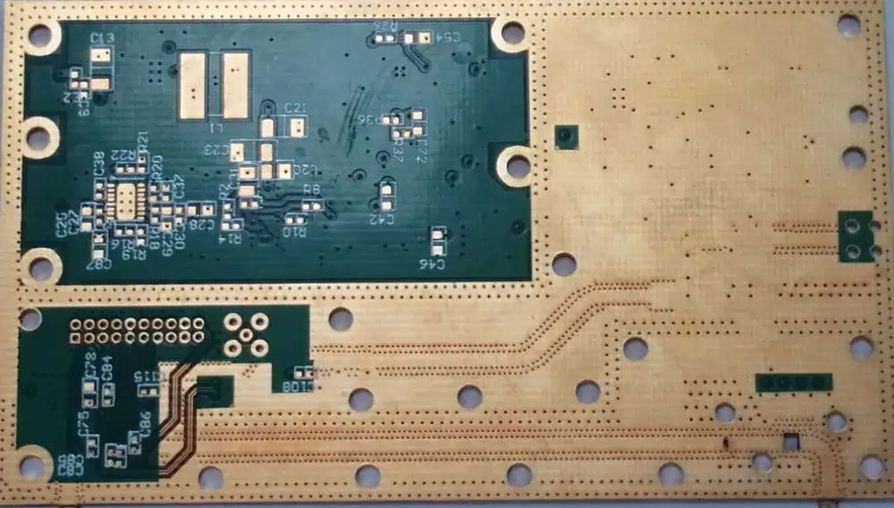
3. Available Grades and Thicknesses

The RO4000 LoPro series typically includes multiple grades optimized for different applications:

3.1 RO4003C LoPro

  • Dk: 3.38 ยฑ 0.05 (10 GHz)
  • Available thicknesses: 0.203 mm (8 mils) to 1.524 mm (60 mils)

3.2 RO4350B LoPro

  • Dk: 3.48 ยฑ 0.05 (10 GHz)
  • Available thicknesses: 0.254 mm (10 mils) to 1.524 mm (60 mils)

3.3 Copper Foil Options

  • Low-profile reverse-treated electrodeposited copper
  • Available weights: 1/2 oz (17 ฮผm), 1 oz (35 ฮผm), 2 oz (70 ฮผm)

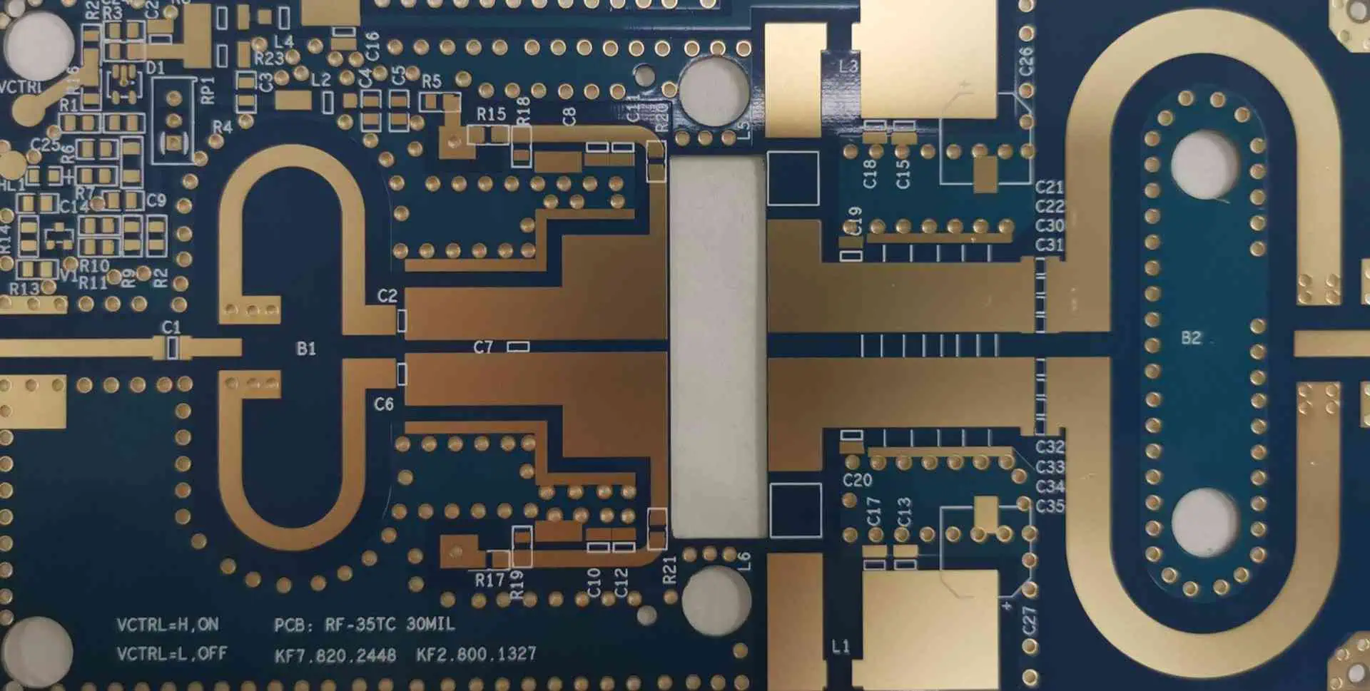
4. Laminate Construction

The datasheet provides information on the laminate construction, which is crucial for understanding its behavior and processing requirements:

  • Glass fabric reinforcement type
  • Resin system composition
  • Copper foil type and treatment

This section may also include details on the material’s uniformity and consistency across the panel.

5. Processing Information

While detailed processing guidelines are usually provided in a separate document, the datasheet may include key processing parameters:

5.1 Lamination

  • Recommended lamination temperature: 182ยฐC to 199ยฐC
  • Recommended lamination pressure: 200-350 PSI

5.2 Drilling

  • Recommended drill speeds and feeds
  • Special considerations for high aspect ratio holes

5.3 Plating and Etching

  • Compatibility with standard plating processes
  • Recommended etchants and process parameters

6. Electrical Performance Data

The datasheet typically includes graphs and charts illustrating the material’s electrical performance:

6.1 Dielectric Constant vs. Frequency

A graph showing how the dielectric constant varies across a wide frequency range, typically from 1 GHz to 50 GHz or higher.

6.2 Dissipation Factor vs. Frequency

A chart illustrating the change in dissipation factor over the same frequency range.

6.3 Insertion Loss Performance

Comparative data showing the insertion loss performance of RO4000 LoPro laminates against other common PCB materials.

7. Environmental and Reliability Data

Information on the material’s performance under various environmental conditions:

7.1 Moisture Absorption

  • Typical value: < 0.1%
  • Test method: IPC-TM-650 2.6.2.1

7.2 Flammability Rating

  • UL 94 V-0

7.3 Lead-Free Process Compatibility

  • Suitable for lead-free soldering processes
  • Maximum temperature resistance

7.4 Chemical Resistance

Data on the material’s resistance to various chemicals commonly used in PCB processing.

8. Regulatory Compliance

The datasheet includes information on the material’s compliance with various industry standards and regulations:

  • RoHS compliance
  • REACH compliance
  • UL certification details

9. Comparison with Other Materials

A section comparing RO4000 LoPro laminates with other Rogers materials and competing products, highlighting its unique advantages.

10. Storage and Handling Recommendations

Brief guidelines on proper storage and handling of the material to maintain its properties and ensure optimal processing:

  • Recommended storage conditions
  • Shelf life information
  • Handling precautions

11. Ordering Information

Details on how to order RO4000 LoPro laminates:

  • Product codes for different grades and thicknesses
  • Standard panel sizes
  • Minimum order quantities

12. Technical Support and Additional Resources

Information on how to obtain technical support and access to additional resources:

  • Contact information for Rogers Corporation’s technical support team
  • Links to processing guides, design tools, and application notes
  • Information on sample availability for testing and evaluation

Conclusion

The RO4000 LoPro laminates datasheet provides comprehensive information on the material’s properties, performance characteristics, and processing requirements. This data is essential for engineers and PCB designers working on high-frequency and high-speed digital applications. By understanding and utilizing the information provided in the datasheet, designers can optimize their circuit designs and ensure optimal performance in demanding RF and microwave applications.

It’s important to note that datasheet information may be updated periodically, and users should always refer to the latest version provided by Rogers Corporation for the most accurate and up-to-date information. Additionally, for specific design requirements or advanced applications, it’s recommended to consult directly with Rogers Corporation’s technical support team.

Rogers RO3000 Series Datasheet PDF & Price (RO3003, RO3003G2, RO3006, RO3010, RO3035, RO3200)

Rogers TC350 PCB

Rogers RO3000 Series are high-performance circuit materials for RF and microwave applications. These ceramic-filled PTFE composites offer low dielectric constants and loss tangents. Detailed specifications are available in the product datasheet. While prices vary based on specific grade and quantity, they’re competitively priced for their performance level. The series includes popular grades like RO3003 and RO3006, each optimized for different frequency ranges and applications.

SeriesRO3003RO3003G2RO3006RO3010RO3035RO3200
DK Value3.00 +/- 0.04minimize Dk variation6.15 +/- 0.15ย 10.2 +/- 0.30ย 3.50 (+/-0.05)10.2
BenefitsLow Dk loss allows for use in applications up to 77 GHzfor 77/79 GHz auto radar designsDissipation factor of .0020 at 10GHz
Material exhibits dimensional stabilityCan be used in applications up to 30-40 GHz
Useful frequency range beyond 40 GHz

Rogers RO3000 Series Datasheet & Price

1. RO3003 Laminates

RO3003 Laminates are high-frequency circuit materials from Rogers Corporation. They offer a low dielectric constant of 3.0, excellent electrical performance, and tight thickness tolerance. These ceramic-filled PTFE composites are ideal for millimeter-wave applications, antennas, and precision stripline circuits.

  • Dk of 3.00 +/- 0.04
  • Dissipation factor of 0.0013 at 10 GHz
  • Available with Rolled Copper

PDF Datasheet Downloads:

2. RO3003G2 Laminates

RO3003G2 Laminates are advanced circuit materials designed for high-frequency applications. With a low dielectric constant of 3.0, they offer excellent electrical performance, low loss, and superior dimensional stability. Ideal for millimeter-wave circuits, antennas, and precision stripline designs.

  • Next generation laminates for 77/79 GHz auto radar designs
  • Very low profile ED copper for lower insertion loss
  • Formulated to minimize Dk variation & enable micro vias

PDF Datasheet Downloads:

3. RO3006 Laminates

RO3006 Laminates are high-frequency circuit materials engineered for RF and microwave applications. With a dielectric constant of 6.15, they provide low loss, excellent dimensional stability, and consistent electrical properties. Ideal for antennas, filters, and high-speed digital circuits.

  • Dk of 6.15 +/- 0.15
  • Higher Dk allows for reduced circuit size

PDF Datasheet Downloads:

4. RO3010 Laminates

RO3010 Laminates are high-performance circuit materials designed for RF and microwave applications. With a dielectric constant of 10.2, they offer excellent electrical stability, low loss, and tight thickness control. Ideal for compact antennas and filters in wireless communication systems.

  • Dk of 10.2 +/- 0.30
  • Higher Dk allows for reduced circuit size

5. RO3035 Laminates

RO3035 Laminates are high-frequency circuit materials designed for microwave and RF applications. They offer excellent electrical performance, low loss, and consistent dielectric constant. These laminates are ideal for antenna systems, power amplifiers, and other demanding high-frequency circuits.

  • Dk of 3.50 (+/-0.05)
  • Dissipation factor of 0.0017 at 10 GHz
  • Available with Rolled Copper

6. RO3200 Series Laminates

RO3200 Series Laminates are high-performance circuit materials by Rogers Corporation. These ceramic-filled PTFE composites offer a dielectric constant of 3.0 to 3.5, low loss, and excellent dimensional stability. They’re ideal for high-frequency, low-noise amplifiers and space-saving multilayer boards.

  • Dk of 10.2
  • Available with Rolled Copper
  • Woven glass reinforcement increases laminate rigidity


RO3000 Series Laminates – PSIS

Rogers-6002-PCB

Rogers RO3000 Series Laminates – PSIS are high-frequency circuit materials designed for demanding RF and microwave applications. These ceramic-filled PTFE composites offer excellent electrical and mechanical stability across a wide range of frequencies. With low dielectric constants and loss tangents, they’re ideal for antenna arrays, power amplifiers, and patch antennas. Their consistent performance and ease of fabrication make them popular choices in the telecommunications and aerospace industries.

Powered By EmbedPress

PCB Materials for Handheld Device Antennas

ADSB Antenna PCB

PCB Materials for Handheld Device Antennas are specialized substrates designed to optimize wireless performance in compact electronics. These materials offer low dielectric loss, consistent electrical properties, and thermal stability. They support high-frequency operations, minimize signal interference, and maintain antenna efficiency. Used in smartphones, tablets, and wearables, these materials enable miniaturization of antennas while ensuring reliable connectivity. Their properties contribute to improved signal quality, extended battery life, and enhanced overall device performance in the competitive handheld electronics market.

Powered By EmbedPress

High Performance Automotive Circuit Materials – Paving the Way

High Performance Automotive Circuit Materials are specialized substrates designed for electronic systems in vehicles. These materials offer superior electrical properties, thermal stability, and reliability under extreme conditions. They support high-speed data transmission, resist electromagnetic interference, and withstand vibrations and temperature fluctuations. Used in advanced driver assistance systems, infotainment, and powertrain control modules, these materials enable lighter, more efficient, and technologically advanced vehicles, meeting the demanding requirements of modern automotive electronics.

Powered By EmbedPress

High Performance Automotive Circuit Materials – Paving the Way

The automotive industry stands at a technological crossroads, where traditional mechanical systems are rapidly giving way to sophisticated electronic architectures. As vehicles evolve from simple transportation devices to complex mobile computing platforms, the demand for high-performance automotive circuit materials has never been more critical. These specialized materials form the backbone of modern automotive electronics, enabling everything from basic engine management to advanced autonomous driving systems.

The Evolution of Automotive Electronics

Modern vehicles contain an astounding array of electronic systems that would have been unimaginable just decades ago. Today’s average car incorporates over 100 electronic control units (ECUs), managing functions ranging from powertrain control and safety systems to infotainment and connectivity features. This electronic proliferation has created unprecedented demands on the circuit materials that support these systems.

The transition toward electric and hybrid vehicles has further intensified these requirements. High-voltage battery management systems, electric motor controllers, and regenerative braking systems all demand circuit materials capable of handling extreme electrical loads while maintaining reliability over extended periods. Additionally, the push toward autonomous driving technologies requires circuit boards that can process vast amounts of sensor data in real-time, necessitating materials with exceptional signal integrity characteristics.

Critical Performance Requirements

Automotive circuit materials must meet stringent performance criteria that far exceed those of consumer electronics. Temperature resilience stands as perhaps the most demanding requirement, as automotive electronics must function reliably across temperature ranges from -40ยฐC to +125ยฐC, with some applications requiring even broader ranges. Under-hood components face particularly harsh conditions, experiencing rapid temperature cycling, vibration, and exposure to automotive fluids.

Electrical performance requirements are equally demanding. High-frequency applications, such as radar systems for collision avoidance and adaptive cruise control, require materials with stable dielectric properties and minimal signal loss. Power electronics applications demand materials capable of handling high current densities while maintaining thermal stability. The increasing prevalence of high-speed digital communications within vehicles necessitates materials with controlled impedance characteristics and minimal electromagnetic interference.

Mechanical durability represents another critical performance dimension. Automotive circuit boards must withstand constant vibration, thermal cycling, and mechanical stress throughout the vehicle’s operational lifetime. This durability requirement extends to the material’s ability to maintain solder joint integrity and resist delamination under stress.

Advanced Material Technologies

The industry has responded to these challenges through the development of specialized high-performance materials. Modern automotive circuit materials typically employ advanced resin systems, such as modified epoxy resins, polyimides, and thermoplastic materials, each offering unique advantages for specific applications.

Thermally conductive materials have gained prominence in power electronics applications. These materials incorporate thermally conductive fillers, such as aluminum oxide or boron nitride, to enhance heat dissipation while maintaining electrical insulation properties. Metal-core printed circuit boards (MCPCBs) represent an extreme example of this approach, featuring metal substrates that provide exceptional thermal management capabilities for high-power LED lighting and power conversion applications.

For high-frequency applications, low-loss dielectric materials have become essential. These materials minimize signal attenuation and maintain stable electrical properties across wide frequency ranges. Advanced ceramic-filled materials and specialized resin systems enable the reliable operation of automotive radar systems, wireless communication modules, and other high-frequency applications.

Flexible and rigid-flexible circuit materials have opened new possibilities for automotive design. These materials enable three-dimensional circuit routing, allowing designers to create more compact and efficient electronic packages while improving reliability by reducing the number of interconnections required.

Emerging Challenges and Solutions

The automotive industry’s rapid evolution continues to present new challenges for circuit material manufacturers. The increasing adoption of wide-bandgap semiconductors, such as silicon carbide and gallium nitride, creates new thermal and electrical stress conditions that traditional materials may not adequately address. These advanced semiconductors operate at higher temperatures and switching frequencies, requiring circuit materials with enhanced thermal conductivity and electrical performance.

The growing emphasis on vehicle electrification has introduced new safety considerations. Circuit materials for high-voltage applications must provide enhanced insulation properties and flame resistance to meet stringent automotive safety standards. Additionally, the need for lightweight materials to improve vehicle efficiency has driven the development of advanced composite materials that maintain performance while reducing weight.

Environmental considerations have become increasingly important in material selection. Automotive manufacturers are demanding materials that comply with environmental regulations while maintaining performance throughout the vehicle’s lifecycle. This has led to the development of halogen-free materials and recyclable substrate options.

Manufacturing and Quality Considerations

The manufacturing of high-performance automotive circuit materials requires sophisticated process control and quality assurance measures. Material suppliers must maintain tight tolerances on electrical, thermal, and mechanical properties while ensuring consistent performance across large production volumes. This consistency is critical for automotive applications, where reliability and predictable performance are paramount.

Quality certification processes for automotive materials are particularly rigorous. Materials must undergo extensive qualification procedures, including accelerated aging tests, thermal cycling evaluations, and vibration testing. These qualification processes can take months or even years to complete, but they are essential for ensuring the long-term reliability of automotive electronics.

Future Directions and Innovations

Looking ahead, several trends are shaping the future of automotive circuit materials. The continued miniaturization of electronic components is driving demand for materials with finer feature capabilities and improved dimensional stability. Advanced packaging technologies, such as embedded component designs and three-dimensional integration, require materials with enhanced processing capabilities.

The integration of artificial intelligence and machine learning capabilities into vehicles is creating new performance requirements. These applications demand circuit materials capable of supporting high-speed data processing while maintaining signal integrity across complex interconnection networks.

Sustainability considerations are becoming increasingly important in material development. Manufacturers are exploring bio-based materials and developing recycling processes for end-of-life circuit boards. These initiatives align with the automotive industry’s broader sustainability goals while maintaining the performance requirements of advanced automotive electronics.

Conclusion

High-performance automotive circuit materials represent a critical enabling technology for the modern automotive industry. As vehicles continue to evolve toward greater electrification, connectivity, and autonomy, the demands placed on these materials will only intensify. The successful development and deployment of advanced circuit materials will be essential for realizing the full potential of next-generation automotive technologies.

The collaboration between material suppliers, circuit board manufacturers, and automotive OEMs will be crucial for addressing the emerging challenges and opportunities in this rapidly evolving field. Through continued innovation and development, high-performance automotive circuit materials will continue to pave the way for the vehicles of tomorrow, enabling safer, more efficient, and more capable transportation solutions for the global community.

RO3003G2 Laminates Data Sheet

Rogers-RO3035-pcb

Rogers RO3003G2 Laminates Data Sheet provides detailed specifications for Rogers Corporation’s high-frequency circuit material. This laminate is designed for millimeter-wave applications up to 77 GHz. It features a low dielectric constant of 3.00, making it ideal for high-speed digital and RF/microwave applications. The data sheet includes information on electrical properties, thermal characteristics, dimensional stability, and processing guidelines. RO3003G2 is known for its excellent electrical performance, low loss, and consistent dielectric constant across frequencies, making it suitable for demanding applications in 5G infrastructure, automotive radar, and aerospace systems.

Powered By EmbedPress

Quick Reference Processing Guidelines RO3000 and RO3200 Laminates

Rogers RO3000 and RO3200 laminates, produced by Rogers Corporation, require specific processing guidelines for optimal performance. These high-frequency materials demand careful handling during drilling, cutting, and lamination. Recommended practices include using sharp drill bits, controlling entry and exit speeds, and maintaining proper lamination temperatures. Copper etching and plating processes should follow manufacturer specifications. Proper storage and handling are crucial to prevent moisture absorption and maintain the laminates’ electrical and mechanical properties.

Powered By EmbedPress

PCB antenna Placement Tips and Tricks

PCB Antenna Layout

Proper PCB antenna placement is crucial for optimal performance. Place antennas away from metal components and high-frequency signals to avoid interference. Ensure a clear ground plane and maintain sufficient distance from other circuitry. Use impedance matching and consider antenna orientation for better signal reception. Test and optimize placement during prototyping for best results.

YouTube video

Don’t lose 90% of total efficiency by poorly placing your PCB antenna!

Main points:
1) Optimal ground plane size is 1/4lambda
2) Keep-out area – no metal around antenna
3) No big metal components near antenna

Powered By EmbedPress

The strategic placement of antennas on printed circuit boards (PCBs) represents one of the most critical aspects of wireless device design. Poor antenna placement can severely compromise signal quality, reduce transmission range, and create interference issues that plague device performance. Understanding the fundamental principles and practical techniques for optimal antenna positioning is essential for engineers developing everything from IoT sensors to high-performance communication devices.

Understanding Antenna Fundamentals in PCB Design

Antennas function by converting electrical energy into electromagnetic waves and vice versa. On a PCB, this conversion process is heavily influenced by the surrounding environment, including ground planes, traces, components, and even the device enclosure. The antenna’s radiation pattern, gain characteristics, and impedance matching all depend critically on its physical placement and the electromagnetic environment created by the PCB layout.

The most fundamental consideration in antenna placement is maintaining a clear radiation pattern. Antennas require unobstructed space to radiate efficiently, and any nearby conductive elements can significantly alter their performance characteristics. This includes not only obvious obstructions like large metal components but also subtle influences from ground planes, power traces, and even small passive components positioned too closely to the antenna element.

Ground Plane Considerations and Keep-Out Zones

Ground planes play a pivotal role in antenna performance, serving as both a reference for the antenna and a potential source of interference. The relationship between the antenna and ground plane must be carefully managed to optimize performance. For most antenna types, maintaining appropriate clearance from ground planes is crucial for preserving the intended radiation pattern and preventing detuning effects.

Establishing proper keep-out zones around antennas is essential for consistent performance. These zones should be free from copper pours, traces, vias, and components that could interfere with the antenna’s electromagnetic field. The size of these keep-out zones varies depending on the antenna type and operating frequency, but generally extends at least one-quarter wavelength from the antenna element in all directions where possible.

The ground plane size and shape also significantly impact antenna performance. For chip antennas and PCB trace antennas, the ground plane acts as a counterpoise, and its dimensions directly affect the antenna’s resonant frequency and radiation efficiency. Insufficient ground plane area can lead to poor antenna efficiency and unpredictable performance variations across different device orientations.

Minimizing Interference from Digital Circuits

Modern PCBs typically combine wireless functionality with digital processing circuits, creating potential interference challenges. Digital switching circuits generate broadband electromagnetic noise that can couple into antenna systems, degrading receiver sensitivity and creating spurious emissions. Careful placement strategies can minimize these interactions and maintain clean RF performance.

Physical separation represents the first line of defense against digital interference. Positioning antennas as far as possible from high-speed digital circuits, crystal oscillators, and switching power supplies helps reduce coupling mechanisms. When physical separation is limited by board size constraints, strategic use of ground planes and shielding techniques becomes critical.

Clock signals and their harmonics pose particular challenges for antenna systems. High-frequency clock edges create broadband noise that can interfere with receiver circuits across multiple frequency bands. Routing clock signals away from antenna areas and using proper grounding techniques helps minimize these effects. Additionally, implementing spread-spectrum clocking can reduce the peak energy at specific frequencies, making interference management more manageable.

Multi-Antenna Systems and Diversity Techniques

Many modern wireless devices incorporate multiple antennas to improve performance through diversity techniques or multiple-input multiple-output (MIMO) systems. The placement of multiple antennas on a single PCB requires careful consideration of mutual coupling effects and correlation between antenna elements.

Antenna spacing plays a crucial role in diversity system performance. For spatial diversity applications, antennas should be separated by at least half a wavelength to ensure sufficient decorrelation between received signals. However, physical constraints often limit achievable spacing, making pattern diversity and polarization diversity attractive alternatives.

Pattern diversity can be achieved by orienting antennas in different directions or using different antenna types with complementary radiation patterns. This approach allows for effective diversity performance even when physical spacing is limited. Polarization diversity employs antennas with orthogonal polarizations, such as combining vertical and horizontal linear polarizations or using circular polarizations of opposite handedness.

Frequency-Specific Placement Strategies

Different frequency bands present unique challenges and opportunities for antenna placement. Low-frequency applications, such as those operating in the 433 MHz or 915 MHz ISM bands, typically require larger antenna structures and more extensive keep-out zones. The longer wavelengths associated with these frequencies make quarter-wave and half-wave antenna elements physically large, often requiring creative placement solutions or the use of loading techniques to reduce antenna size.

Higher frequency applications, including 2.4 GHz Wi-Fi, Bluetooth, and 5 GHz systems, benefit from smaller antenna structures but face increased sensitivity to nearby objects and manufacturing tolerances. The shorter wavelengths make these systems more susceptible to detuning effects from nearby components and mechanical variations in the manufacturing process.

Millimeter-wave applications, such as those used in 5G communications and high-resolution radar systems, present extreme challenges for PCB antenna placement. The very short wavelengths make these systems highly sensitive to even minor placement variations, requiring precise design practices and careful attention to manufacturing tolerances.

PCB Stack-Up Considerations

The PCB stack-up significantly influences antenna performance, particularly for antennas implemented directly on the PCB using copper traces. The dielectric constant and loss tangent of the PCB substrate material affect the antenna’s resonant frequency, bandwidth, and efficiency. These effects must be considered during the design phase and may require antenna geometry adjustments to compensate for the substrate properties.

Multi-layer PCB designs offer opportunities for improved antenna integration through the use of dedicated antenna layers and optimized ground plane configurations. However, the increased complexity of multi-layer designs also introduces additional variables that can affect antenna performance, including layer-to-layer registration tolerances and via placement effects.

Mechanical and Thermal Considerations

Antenna placement must account for mechanical stress and thermal effects that can occur during device operation and environmental exposure. Antennas positioned near mechanical stress points or areas subject to significant temperature variations may experience performance degradation over time. This is particularly important for devices intended for automotive, industrial, or outdoor applications where environmental conditions can be severe.

Thermal management becomes critical when antennas are placed near power-dissipating components. Elevated temperatures can affect the electrical properties of antenna materials and nearby dielectric substrates, potentially causing frequency shifts and performance degradation. Proper thermal design practices, including the use of thermal vias and heat spreaders, help maintain stable antenna performance across the intended operating temperature range.

Testing and Validation Strategies

Successful antenna placement requires comprehensive testing and validation to ensure performance meets design requirements across all intended operating conditions. This includes both simulation-based analysis during the design phase and physical measurements of prototype hardware. Antenna measurement techniques must account for the complete system environment, including the effects of nearby components, enclosures, and user interaction.

Over-the-air testing in realistic environments provides the most accurate assessment of antenna system performance. This includes evaluation of radiation patterns, gain characteristics, and interference susceptibility under conditions that closely match the intended application. Such testing often reveals performance issues that are not apparent in idealized simulation environments or laboratory measurements.

Conclusion

Effective PCB antenna placement requires a comprehensive understanding of electromagnetic principles, careful attention to design details, and systematic validation through simulation and measurement. The techniques and considerations outlined here provide a foundation for achieving optimal antenna performance in modern wireless devices. Success in antenna placement comes from balancing competing requirements while maintaining focus on the specific performance metrics most critical to the intended application. As wireless technologies continue to evolve and integrate into increasingly compact devices, these fundamental principles remain essential for achieving reliable and efficient wireless communication systems.

SMD LED vs COB LED vs DOB LED – 3 Options for LED PCBs

Introduction

Light Emitting Diodes (LEDs) have revolutionized the lighting industry, offering energy-efficient and long-lasting solutions for various applications. As technology advances, different types of LED configurations have emerged to cater to specific needs and preferences. This article will explore three popular options for LED PCBs: Surface Mount Device (SMD) LEDs, Chip on Board (COB) LEDs, and Direct on Board (DOB) LEDs. We’ll delve into their characteristics, advantages, disadvantages, and applications to help you make an informed decision for your lighting projects.

Understanding LED PCBs

Before we dive into the specifics of SMD, COB, and DOB LEDs, it’s essential to understand the role of Printed Circuit Boards (PCBs) in LED technology. PCBs serve as the foundation for mounting and connecting electronic components, including LEDs. They provide mechanical support, electrical connections, and heat dissipation, which are crucial for the performance and longevity of LED systems.

SMD LED: Surface Mount Device

What is SMD LED?

Surface Mount Device (SMD) LEDs are compact, pre-packaged LED chips that can be directly mounted onto the surface of a PCB. They are widely used in various lighting applications due to their versatility and ease of integration.

Characteristics of SMD LEDs

  1. Size and Package: SMD LEDs come in various package sizes, typically ranging from 2835 (2.8mm x 3.5mm) to 5050 (5.0mm x 5.0mm).
  2. Components: Each SMD LED package contains one or more LED chips, a reflector cup, and wire bonding.
  3. Color Options: Available in a wide range of colors, including white, RGB, and multi-color configurations.
  4. Luminous Efficacy: Typically ranges from 100 to 160 lumens per watt, depending on the specific model and manufacturer.

Advantages of SMD LEDs

  1. Versatility: Can be used in various applications, from small electronics to large-scale lighting projects.
  2. Color Mixing: Easy to create multi-color or tunable white light solutions.
  3. Heat Dissipation: Generally good heat dissipation due to the spread-out nature of individual LEDs.
  4. Customization: Allows for flexible design and customization of light output and distribution.

Disadvantages of SMD LEDs

  1. Individual Mounting: Each LED must be individually placed on the PCB, which can be time-consuming for large-scale production.
  2. Potential for Non-Uniform Light: If not properly designed, may result in visible individual light sources or hot spots.
  3. More Components: Requires more components compared to COB or DOB LEDs, potentially increasing the risk of failure points.

Applications of SMD LEDs

  • LED strips and tape lights
  • Backlighting for displays and signage
  • Automotive lighting
  • General indoor and outdoor lighting fixtures

COB LED: Chip on Board

What is COB LED?

Chip on Board (COB) LED technology involves mounting multiple LED chips directly onto a substrate to form a single module. This results in a more compact and powerful light source compared to individual SMD LEDs.

Characteristics of COB LEDs

  1. Size and Package: COB LEDs are typically larger than SMD LEDs, with sizes ranging from 9mm to 30mm or more.
  2. Components: Multiple LED chips are mounted directly on a substrate and covered with a layer of phosphor (for white light).
  3. Color Options: Primarily available in white light with various color temperatures, though RGB options exist.
  4. Luminous Efficacy: Generally higher than SMD LEDs, ranging from 130 to 200 lumens per watt.

Advantages of COB LEDs

  1. High Lumen Density: Produces a large amount of light from a small area.
  2. Uniform Light Output: Creates a more even light distribution without visible individual light sources.
  3. Improved Thermal Management: Better heat dissipation due to direct mounting on the substrate.
  4. Simplified Manufacturing: Easier to assemble and requires fewer components than multiple SMD LEDs.

Disadvantages of COB LEDs

  1. Limited Color Options: Primarily available in white light, with fewer multi-color options compared to SMD LEDs.
  2. Less Flexibility in Design: The fixed nature of the COB module limits customization options.
  3. Higher Initial Cost: Generally more expensive per unit compared to SMD LEDs.
  4. Potential for Glare: The high lumen density can cause glare if not properly diffused or directed.

Applications of COB LEDs

  • High-bay lighting for warehouses and industrial spaces
  • Spotlights and track lighting
  • Street and area lighting
  • Automotive headlights

DOB LED: Direct on Board

What is DOB LED?

Direct on Board (DOB) LED technology is the latest innovation in LED lighting. It involves mounting LED chips directly onto the main PCB without the need for a separate substrate or package.

Characteristics of DOB LEDs

  1. Size and Package: DOB LEDs are integrated directly into the PCB, allowing for very thin and compact designs.
  2. Components: LED chips are mounted directly on the main PCB along with other necessary components.
  3. Color Options: Available in various color temperatures of white light, with some RGB options.
  4. Luminous Efficacy: Comparable to or slightly higher than COB LEDs, ranging from 150 to 220 lumens per watt.

Advantages of DOB LEDs

  1. Simplified Manufacturing: Eliminates the need for a separate LED package or module, streamlining production.
  2. Improved Thermal Performance: Direct contact with the PCB allows for better heat dissipation.
  3. Cost-Effective: Reduces overall production costs by eliminating intermediate components and assembly steps.
  4. Ultra-Thin Designs: Enables the creation of extremely thin and lightweight lighting fixtures.

Disadvantages of DOB LEDs

  1. Limited Availability: As a newer technology, there may be fewer suppliers and options compared to SMD or COB LEDs.
  2. Specialized Equipment: May require specialized manufacturing equipment and processes.
  3. Repair Challenges: In case of LED failure, the entire PCB may need to be replaced.
  4. Design Constraints: The integration of LEDs directly on the PCB may limit some design flexibility.

Applications of DOB LEDs

  • Flat panel lights
  • Ultra-thin downlights
  • Linear lighting fixtures
  • Automotive interior lighting

Comparison of SMD, COB, and DOB LEDs

To better understand the differences between these three LED PCB options, let’s compare them across various parameters:

ParameterSMD LEDCOB LEDDOB LED
SizeSmall, individual packagesLarger, single moduleIntegrated into PCB
Lumen DensityModerateHighHigh
Color OptionsWide range, including RGBPrimarily white, limited RGBPrimarily white, some RGB
Heat DissipationGoodBetterBest
CostLow to moderateModerate to highModerate
Manufacturing ComplexityModerateLowLowest
CustomizationHighLimitedModerate
Luminous Efficacy (lm/W)100-160130-200150-220
Glare PotentialLowHighModerate
Repair/ReplacementEasyModerateDifficult

Choosing the Right LED PCB Option

When selecting between SMD, COB, and DOB LEDs for your project, consider the following factors:

  1. Application: Determine the specific lighting requirements for your project.
  2. Light Output: Consider the desired lumen output and distribution pattern.
  3. Color Requirements: Decide if you need white light, specific color temperatures, or RGB capabilities.
  4. Space Constraints: Evaluate the available space for the lighting fixture.
  5. Thermal Management: Assess the heat dissipation needs of your application.
  6. Cost Considerations: Balance initial costs with long-term energy efficiency and maintenance.
  7. Manufacturing Capabilities: Consider your production volume and available manufacturing processes.

Application-Specific Recommendations

ApplicationRecommended LED TypeReasoning
LED StripsSMD LEDFlexibility and color options
High-Bay LightingCOB LEDHigh lumen output and uniform distribution
Ultra-Thin PanelsDOB LEDCompact design and efficient heat management
Automotive LightingSMD or COB LEDVersatility for different automotive applications
Outdoor LightingCOB or DOB LEDHigh efficiency and good thermal management
Decorative LightingSMD LEDWide color range and design flexibility

Future Trends in LED PCB Technology

As LED technology continues to evolve, we can expect to see further improvements in efficiency, cost-effectiveness, and application-specific solutions. Some potential trends include:

  1. Increased DOB LED Adoption: As manufacturing processes improve, DOB LEDs may become more prevalent across various lighting applications.
  2. Hybrid Solutions: Combinations of different LED types on a single PCB to optimize performance for specific use cases.
  3. Advanced Thermal Management: Development of new materials and designs to further improve heat dissipation.
  4. Smart Integration: Incorporation of sensors and control systems directly into LED PCBs for improved functionality and energy efficiency.
  5. Micro-LED Technology: Advancements in extremely small LED chips may lead to new possibilities in display and lighting applications.

Conclusion

SMD, COB, and DOB LEDs each offer unique advantages and are suited for different applications in the world of lighting. SMD LEDs provide versatility and color options, COB LEDs offer high lumen density and uniform output, while DOB LEDs excel in thermal management and manufacturing simplicity. By understanding the characteristics, pros, and cons of each option, you can make an informed decision for your specific lighting project. As LED technology continues to advance, we can expect even more efficient and innovative solutions to emerge, further revolutionizing the lighting industry.

Frequently Asked Questions (FAQ)

1. Which LED type is best for energy efficiency?

While all three types are energy-efficient, DOB LEDs generally offer the highest luminous efficacy, followed closely by COB LEDs. However, the overall energy efficiency of a lighting system depends on various factors, including the specific product, driver efficiency, and thermal management.

2. Can I replace SMD LEDs with COB or DOB LEDs in existing fixtures?

In most cases, it’s not a straightforward replacement due to differences in size, power requirements, and heat dissipation. It’s usually best to design fixtures specifically for the chosen LED type. However, some modular systems may allow for easier upgrades or replacements.

3. Are COB LEDs always better than SMD LEDs for high-power applications?

While COB LEDs are often preferred for high-power applications due to their high lumen density and better thermal management, SMD LEDs can still be suitable in some cases. The choice depends on factors such as the specific power requirements, desired beam angle, and color mixing needs.

4. How do I determine which LED type is best for my project?

Consider factors such as the required light output, color options, space constraints, thermal management needs, and budget. It’s often helpful to consult with lighting designers or engineers who can provide expertise based on your specific project requirements.

5. Are DOB LEDs more expensive than SMD or COB LEDs?

Initially, DOB LEDs may have a higher cost due to the newer technology and potentially specialized manufacturing processes. However, they can be more cost-effective in the long run due to simplified manufacturing, improved thermal management, and potentially longer lifespans. As the technology becomes more widespread, costs are likely to decrease.

Fabrication Guidelines RO3000 and RO3200 Series High Frequency Circuit Materials

Rogers AD255C PCB

Rogers RO3000 and RO3200 Series High Frequency Circuit Materials, developed by Rogers Corporation, are designed for high-frequency, high-speed digital applications. Fabrication guidelines for these materials emphasize careful handling to maintain dimensional stability and electrical performance. Key considerations include using sharp cutting tools, controlling drilling speeds and pressures, and implementing proper copper etching techniques. Temperature management during lamination and drilling is crucial to prevent material degradation. Plated through-hole processes require attention to chemistry and cycle times. These materials offer excellent electrical properties and are compatible with standard PCB fabrication processes when following recommended guidelines, ensuring optimal performance in demanding RF and microwave applications.

Powered By EmbedPress