ADM2682EBRIZ: A Digital Isolator Powered with the Magnetic Coupling Technology

ADM2682EBRIZ

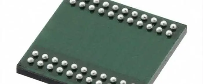
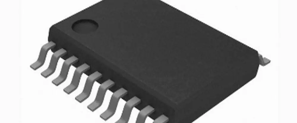
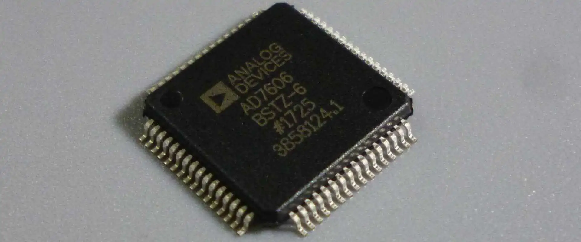
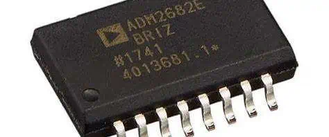
Can an isolated device, let alone a digital isolator work alone? It appears to be so and that is what we have seen in ADM2682EBRIZ. It is a fully-integrated 5 kV signal and power-isolated data transceiver, equipped with some of the best security architectures.

In this article, we talk about the isolatorโ€™s role in circuit boards and some of the technical properties.

The ADM2682E Background

ADM2682E or ADM2687E are two of the digital isolator families by Analog Devices Incorporated. They are designed to be fully-integrated, 5 kV signal and power-isolated data transceivers, optimized for the multipoint transmission lines and high-speed communication markets.

Little wonder why these isolators are used to create a dedicated isolation pathway for a wide range of applications, including the industrial field networks and isolated RS-422 interfaces.

On its part, ADM2682EBRIZ uses a unidirectional channel, and a magnetic coupling technology.

Continue reading to learn more about this digital isolator.

The Relevance of ADM2682EBRIZโ€™s Magnetic Coupling

FULL PCB MANUFACTURING Quote

Different process technologies are deployed when building digital circuits. The most popular are Surface Mount Technology (SMT) and Through-Hole Technology (THT). However, there are more of these process technologies out there. The Magnetic Coupling technology is one of those.

According to GlobalSpec, magnetic coupling has to do with the โ€œnon-contact couplings that use a magnetic field to transfer torque, force or movement from one rotating member to another.โ€

The idea is that using a magnetic coupling technology helps to solidify the synergy among the component-parts of the ADM2682EBRIZ.

Wondering why this is important? Bartleby affirms that using magnetic coupling technology goes a long to facilitate the transfer of energy from one component-part or device to the other(s).

Thus, ADM2682EBRIZโ€™s configuration with magnetic coupling helps in fast-tracking the transfer of electric energy from one circuit to the other.

These are some of the reasons why it is a great process technology:

1. Less Heat Dissipation

Heat dissipation or thermal energy production is one important consideration to make when building a digital circuit. You want to be sure that there is an exposed pad or any other source of heat dissipation pathway to get rid of the excessive heat generated in the process of building and using the circuit board.

On the contrary, you can count on the ADM2682EBRIZ to effectively manage heat dissipation, because it doesnโ€™t generate much in the first place.

2. Flexible Movement

Since ADM2682EBRIZ doesnโ€™t encounter much friction, the same can be extended to the component-parts, thereby, promoting an excellent interaction.

3. Less Noise

Noise pollution is minimal too because magnetic coupling technology produces less noise, than is obtainable with some other circuit board process technology.

4. The isoPower Technology

ADM2682EBRIZโ€™s magnetic coupling is not the only process technology used with the circuit board. It also uses the isoPower Technology.

How does it work? The isoPower Technology works by using a variety of high-frequency switching elements to switch, move or transfer power (current) via the transformer.

5. Integrated Isolation Capabilities

As an integrated and power-isolated transceiver, ADM2682EBRIZ ensures that it offers a one-stop solution. The solution therein is offered in the form of an integrated 5 kV rms isolated dc-to-dc power supply. The integration of this solution helps to cut out the need for any other (external) dc-to-dc isolation block.

6. Balanced Current and Thermal Properties

One of the limitations to working on digital circuits is unstable current or power. From damaging the board to causing serious damages to the components, there are lots of disadvantages to an unstable current.

ADM2682EBRIZ addresses that with the fair balancing of the current (power) and thermal (heat) perspectives. For example, it has a current limiting feature, which helps in keeping the circuit board safer in output short circuits. The thermal shutdown feature sees to the shutting down of the digital circuitโ€™s heat dissipation when it becomes excessive.

How the 5000Vrms Voltage Isolator Works

ADM2682EBRIZ uses the 5000Vrms voltage isolator โ€“ one of the best out there. It is a type of digital isolator that separates the different (digital) circuits.

Although it separates these circuits, it doesnโ€™t entirely leave them to it. Rather, the 5000Vrms voltage isolator still paves the way for signals or current to be transferred between or among the separated circuits.

Mono-Package Integration

To combine most of the important elements into one package, ADM2682EBRIZ uses the iCoupler technology. It is a process technology by Analog Devices Incorporated, the same company that manufactures ADM2682EBRIZ.

By using this process technology, ADM2682EBRIZ allows the target devices to integrate or combine the trio of a differential input receiver, 3-channel isolator and a three-state differential line driver.

It also combines the isoPower process technologyโ€™s dc-to-dc converter with the above into a single package.

This method doesnโ€™t only keep the most significant components under โ€œone roofโ€ but also enhances the actualization of the RS-485 isolated solution via the combination of the 3.3 volts and the 5 volts single power supply.

ADM2682EBRIZโ€™s Technical Properties

Below are some of the core properties of the ADM2682EBRIZ digital isolator:

  • Maximum propagation delay of 100 nanoseconds (ns).
  • It supports up to three (3) channels.
  • The maximum rise and fall time are 15 nanoseconds (ns).
  • The operating temperature is between 40หšC and 85หšC.
  • The minimum common mode transient immunity is pegged at 25kV/ยตs
  • ADM2682EBRIZโ€™s voltage supply is between 3.3 volts and 5 volts.

ADM2682EBRIZ Supports Multiple Safety Protocols

Security is of the utmost importance, irrespective of the target applications. ADM2682EBRIZ upholds security and that is evident both in the wide range of supported safety controls and the embedded security architecture.

For the built-in security, it uses the ยฑ15 kV ESD protection on the RS-485 Input and Output (I/O) pins.

It also supports open-and-short circuit, with the fail-safe receiver inputs.

For the safety protocols, it aligns with the following:

  • VDE Certificates of Conformity
  • UL Recognition
  • CSA Component Acceptance Notice #5A

Wrapping Up

ADM2682EBRIZ is not yet obsolete, so you can get your hands on it. In addition, Analog Devices Incorporated, the manufacturer, has some other devices you may want to check out. On the list are the ADUM4160BRWZ-RL and the MAX22245BAWA+.

How Does the ADM3252EABCZ Digital Isolator Work?

ADM3252EABCZ

Integrated Circuits (ICs) come in different forms and usually have one role to play โ€“ to improve the overall functions of the applications or devices. Today, these ICs have been modeled into different forms, with each of these variants offering unique attributes to the target applications.

One of such models is the digital isolator, of which the ADM3252EABCZ is one them. In this article, you will learn how this digital isolator works.

What is a Digital Isolator?

According to Digi-Key, a digital isolator is an electrically-separating Integrated Circuit (IC), which helps in transferring digital signals among the separated circuits.

You want to rely on ADM3252EABCZ to separate signals coming to the circuits, while maintaining the status quo of improving the workings of the target applications.

The Isolation in Force

Is there any need to isolate the electronic signals? Yes, it helps in keeping each of the circuits fully functional and independent.

For this to work effectively, ADM3252EABCZ has been optimized with a series of isolation technologies, one of which is the isoPower integrated technology. The highpoint of this technology is the support for Digital-to-Digital (dc-to-dc) conversion.

This is imperative, seeing that at the core of the isoPower technology is the separation or isolation of the circuits. Thus, it may be impossible for an analog circuit to interface with a digital circuit and vice-versa. Therefore, the dc-to-dc isolated converter is a welcome development.

The 3.3-V Logic Receiver

ADM3252EABCZ uses a variety of logics, one of which is the 3.3-V logic receiver. But before delving into this, we want to mention that this circuit isolator has a dedicated transmitter driverย that converts the 3.3-volts logic input levels into the corresponding RS-232 output levels.

For the 3.3-volts logic receiver, it is tied to the EIA/TIA-232E specifications. As such, it provides for the acceptance of the RS-232 input levels via its dedicated inverting level shifter. This inverting level shifter is responsible for the translation or conversion of the RS-232 input levels into the corresponding 3.3-volts output levels.

ADM3252EABCZโ€™s 3.3-volts logic receiver also works well with the noise impedance, irrespective of the density. For example, its logic receiver uses the Schmitt trigger input with a hysteresis level of 0.1-volt to keep the noisy input and the slow transition input free from errors.

Overvoltage or an excessive supply of current could potentially reduce the potentials of a circuit. That is why the ADM3252EABCZโ€™s pull-down resistor measured at 5 kโ„ฆ is in place. It helps to protect the logic receiver against overvoltage, especially if it measures above ยฑ30 V.

Data Rate

The speed of transferring data to, from and across the circuits is an important consideration when choosing a digital isolator. ADM3252EABCZ has an estimated data rate of 460 kilobytes per second. This is in conformation to the EIA/TIA-232E and the ITU-T V.28 specifications.

Although this is the maximum data rate, as per the datasheet, it is tied to one factor. For the data rate to clock up to that figure, it is expected that the higher data rates of 460 kbps are feasible, only when the ADM3252EABCZ is running at a reduced RS-232 capacitive load levels.

Below is a list of the additional technical specifications of this ADM3252EABCZ, represented in a table:

Technical SpecificationsDescription
Type of ChannelUnidirectional
Technology UsedMagnetic Coupling Technology
Common Mode Transient Immunity (minimum)25kV/ยต
Typical Rise and Fall TimeMaximum of 2.5 nanoseconds (ns)
Number of Channels Used4
Power IsolationYes
Operating Temperature (minimum to maximum)Between 40หšC and 85หšC
Voltage (isolation)2500Vrms
Types of Packages44-LBGA and CSPBGA
Voltage Supply (minimum to maximum)3 volts to 5.5 volts

ADM3252EABCZโ€™s Power Transfer Process

FULL PCB MANUFACTURING Quote

Since ADM3252EABCZ uses the digital isolator framework and combines it with the magnetic coupling technology, how then does it transfer power?

The power, voltage or current transmission process is enabled by the isoPower technology. It uses a set of high-frequency switching elements to transfer, move or return power to the different โ€œisolatedโ€ circuits. All these are done via the dedicated transformer.

The Commonplace for Total Isolation

Even though the separated circuits get power transmitted to and from them with ease, ADM3252EABCZ still maintains the isolation capabilities. To keep this running, it uses the chip-scale iCoupler technology to enable a total isolation solution. This isolation involves the separation or isolation of the dedicated dc-to-dc converter from the logic signals.

Digital Isolator Protection Features

ADM3252EABCZ complies with the Electrostatic Discharge (ESD) standards of protecting circuits, and in extension, consumer electronics.

The highpoint of the protection is the fine-tuning of the target deviceโ€™s security framework in line with the IEC 61000-4-2 system-level testing specifications for ESD devices. The specifications highlight the subjection of the device to a system-level test to confirm the viability to survive normal operations.

To that end, both the Contact Discharge and the Air Gap Discharge have been designed to shore up these specifications.

ADM3252EABCZ uses these two discharge options to meet the ESD system-level testing specifications.

The Air Gap Discharge, according to Maxim Integrated, is a โ€œmethod of testing ESD-protection structures in which the ESD generator is discharged through an air gap.โ€

Typically, the discharge takes place between the Device Under Test (DUT), which, in this case, is the ADM3252EABCZ; and the generator. Therefore, the DUT is to be placed close to the ESD test gun to confirm a discharge.

On the other hand, the Contact Discharge has to do with the ESD system-level testing that involves the discharge of the Electrostatic Discharge (ESD) pulse from the ESD test gun. The pulse is discharged directly to the Device Under Test (DUT).

By default, the ESD system-level testing process specifies the equivalenting of these discharge processes. For that purpose, the Level standard is used to make a Contact Discharge of 8 kV to be equivalent to the 15 kV Air Discharge.

That is exactly the ESD protection rating on ADM3252EABCZ. The Contact Discharge is pegged at ยฑ8 kV, while the Air Discharge is pegged at ยฑ15 kV.

Conclusion

ADM3252EABCZ isolates or separates circuits (electrically) to help them function independently, while using a total of 4 channels to switch the signals unidirectionally.

The Performance of ADP5054ACPZ-R7โ€™s DC DC Switching Controller

ADP5054ACPZ-R7

ADP5054ACPZ-R7 is a DC DC switching controller with a transistor driver output. In this article, we break down the concept of a DC DC switching controller and all the technical specifications of ADP5054ACPZ-R7.

How Does a DC DC Switching Controller Work?

DC DC switching controller is a type of Power Management Integrated Circuit (PMIC). The controller plays a significant role in consumer electronics by aiding the voltage regulation process.

Now, voltage or current can be excessive for a number of factors and it is the duty of the DC DC switching controller to keep the performance at the optimum. For this to work, the controller first generates the output supply voltages either below or above the input supply.

By doing that, it helps to balance the voltage of the high-efficient circuits at the best performance through the current alternation between the input and output voltages.

If you are using a DC DC switching controller, you can be sure that the excessive voltage will be regulated using different means. The processes include but are not limited to:

  • Push-pull
  • Buck-boost
  • Half bridge
  • Flyback
  • SEPIC

ADP5054ACPZ-R7โ€™s Features

FULL PCB MANUFACTURING Quote

ADP5054ACPZ-R7 packs a wide range of features or characteristics that make it one of the best DC DC switching controllers.

In this section, we are going to talk about some of these features.

1. Start Function

Voltage or current can be excessively โ€œrushed intoโ€ the circuits depending on how the switching controller starts or boots. That is the reason why ADP5054ACPZ-R7โ€™s start function combines a variety of functions.

First, there is the precharged start-up feature, which prevents the low-side FETs from getting damaged during the boot process.

Second, a majority of ADP5054ACPZ-R7โ€™s buck regulators use a soft start circuitry, which aids in limiting the current of flow of voltage once the controller is started.

2. Direct Connection to High-Input Voltages

ADP5054ACPZ-R7 is by default, equipped with four (4) high-performance buck regulators. These regulators are packed in a 48-lead LFCSP package.

In addition to the optimization according to board space requirements and system performance, the regulators also establish a direct connection without using any of the preregulators. The outcome? A seamless connection to the high-input voltages, up to 15.5 volts.

3. Power Savings Mode (PSM)

Conserving power is also a part of the features that set ADP5054ACPZ-R7 apart from the other DC DC switching controllers.

The Power Savings Mode (PSM) works by enabling a smooth transition of the buck regulators to the variable frequency.

Note that the Power Savings Mode (PSM) is typically activated when the output of the controller falls below the preset or predefined value/threshold of the PSM.

The activation of the Power Savings Mode (PSM) enables the buck regulators to remain the mode for a few oscillator cycles. The buck regulators would only be taken out of the PSM and restored to the default settings after voltage increases to the PSMโ€™s threshold.

4. Technical Specifications

The table below shows some of the technical attributes of the ADP5054ACPZ-R7 DC DC switching controller:

AttributesDescription
Mounting TypeSurface Mount Technology (SMT)
Maximum Duty Cycle50%
Type of OutputTransistor Driver
Operating Temperature (minimum to maximum)40หšC to 125หšC
TopologyBuck
Frequency Switching CapabilitiesBetween 250kHz to 2MHz
Output ConfigurationPositive
Control FeaturesPower Good, Enable and Frequency Control
FunctionStep-Down
Type of Case/Package48-WFQFN Exposed Pad, CSP
Number of Output Phases2
Synchronous RectifierYes
Number of Outputs4

5. ADP5054ACPZ-R7โ€™s Transistor Driver Output

ADP5054ACPZ-R7 uses a transistor driver as the output and this section is dedicated to explaining how it works.

A transistor driver is generally viewed as a โ€œcurrent amplifierโ€ in the sense that it magnifies or increases the current in any consumer electronics or circuit it is placed. It is typically used to โ€œdriveโ€ or provide sufficient current to the target device without necessarily amplifying or increasing the voltage.

Transistor drivers are also designed to drive the โ€œhigh-power applications,โ€ thus, increasing the performance in the process. To that end, you can expect the transistor to get hotter at some point.

A better way to tackle the excessive heat is to use a thermal transfer compound paste, which helps in improving the heatsinkโ€™s efficiency.

You should also consider installing a heatsink. Attaching the heatsink to the transistorโ€™s tab helps in cooling it when it gets hotter.

Important Considerations for the ADP5054ACPZ-R7 DC DC Switching Controller

Before you are sold on the idea of getting the ADP5054ACPZ-R7, we would like to make a few more submissions.

These are some of the additional considerations you may want to make before deciding to get the switching controller:

Thermal Shutdown Capabilities

Everything is not left to chance, as far as the ADP5054ACPZ-R7 is concerned. It keeps the power optimum, while ensuring that the heat dissipation is excellent.

It also has a thermal shutdown capability, designed to oversee the shutting down of the IC. The thermal shutdown feature kicks in when the junction temperature goes above 150หšC.

The junction temperature tends to shoot above the recommended temperature of 150หšC only when certain factors come to play. From the increase in the ambient temperature to a higher current operation and a poor circuit board design; these factors can negatively impact the junction temperature.

Now, when the junction temperature goes above 150หšC, the Thermal Shutdown (TSD) circuit would then kick in to regulate it. The regulation is done in the form of turning off the Integrated Circuit (IC), while keeping the internal linear regulator on.

However, ADP5054ACPZ-R7 is not quick to restore the circuit to operation until certain measures have been put in place. The first measure is to integrate a 15หšC hysteresis to prevent the circuit board from returning to the normal operations.

Once that is done, the ADP5054ACPZ-R7 wouldnโ€™t become operational, until the on-chip temperature has fallen below 135หšC.

It is only when this has been attained that the ADP5054ACPZ-R7 would initiate the soft start function to slowly activate the circuit for operations after exiting the Thermal Shutdown (TSD) mode.

Precision Enabling

ADP5054ACPZ-R7 has a precision enable pin on each of the channels. The pin, among many other things, aid the power-up sequencing of the circuit board.

Final Words

ADP5054ACPZ-R7 uses the DC DC switching controller to regulate (excessive) voltage, protect the circuit and balance the performance of the components.

Understanding the Concept of ELIC PCB Assembly and Manufacturing

hdi PCB Manufacturers

The manufacturing of PCBs makes them equipped with multiple layers, and they are thin in size. It is due to the usage of different methods that enhance the interconnect density.

The name of the technology is Every Layer Interconnect (ELIC), which helps to produce extremely thin and functional circuits.

Additional features rendered by these HDI boards include layers filled with copper and come with in-pad micro vias that allow smooth and flawless interconnections. 

Designing an ELIC PCB Stackup

FULL PCB MANUFACTURING Quote

ELIC is also called any-layer HDI. It means that any layer in the stack has the ability to conduct signals based on high-density interconnects present between all the layers. The features of individual layers are copper-filled, laser-drilled micro vias.

ELIC relies on copper-filled micro vias, which is useful for producing functional connections among the layers. The benefits of this method include connections between any two layers in the PCBs after the layers are all stacked.

Another good advantage is that it is flexible, and the producer of PCBs can use it to magnify the interconnect density present on any layer.

ELIC PCB Manufacturing

The ELIC manufacturing process starts with two major things. These are ultra-thin cores with laser micro vias along with a solid copper base. The micro vias are filled with copper internally. The next step is to include a dielectric layer during the process of lamination.

Laser drilling is on the recent layer to complete the ELIC PCB stack. The process is conducted in a loop unless the desired PCB stack develops that contains copper-packed micro vias.

The benefit of using copper filling is the structural integrity of the board. Another reason to use this filling is to prevent dimpling/voiding in the interior micro vias. 

Advantages and Characteristics of ELIC PCB 

1. Smaller Size

HDI PCB can invite many circuit parts even if there is little space for installation. It helps to produce portable devices that contain the ability to consume less electricity.

Such a technique is useful in the manufacturing of smartwatches and other compact smart devices.

2. Options of Flexible Mounting

ELIC PCB is also malleable and reformable from the corners. During this action, it does not get damaged at all.

Its flexibility and no use of an external coating like conformal coatings (CC) make this whole process free of technical complications.

It works best with former versions of rigid PCB, which do not allow flexible bending and other reformations. 

3. Faster Speed

ELIC HDI PCBs work faster in terms of functioning. These functions include processing and data transfer rates at a rapid speed for efficient execution.

Such a benefit is useful when there is a need for devices for processing huge datasets and large files transmission that typically happens in cellular communications. This strategy is useful in PGA chipsets or discrete components for ELIC PCBs. 

4. Excellent Heat Dissipation Performance

The feature of heat dissipation of ELIC HDI PCBs is due to the assembling of a special copper foil that acts as a substrate material for these circuits.

It produces extremely impressive thermal conductivity, which helps in quick and effective heat dissipation during any kind of action. Such devices are useful to make industrial robots and semiconductors efficient in their performance. 

5. Short Lead Time

It needs much lesser time for the entire manufacturing. The process of production is not extensive, which is why it takes little time the completion.

For instance, FR-4 boards and glass fiber boards are easier to produce when the production process is simpler and takes less time. 

6. High Reliability

ELIC HDI PCBs feature anti-jamming capability, which makes them more reliable than former versions of the PCBs.

The benefits are the huge endurance of high temperatures, humidity, static electricity, and electromagnetic interference (EMI).

These can work well due to such attributes in the areas of oil fields, chemical plants, power plants, and military equipment applications.

Applications of ELIC PCB

ELIC is a major component f the PCBs which are used in GPUs and memory cards. Today, the devices like smart phones, tablets, and wearable smart gear are also working with ELIC.

The attributes like high pin count and fine pitch are the plus points of these devices.

The layer count in these devices is limited to 10. This strategy helps the producers and designers with desired interconnect in boards with a small footprint.

ยท High-Speed

ELIC PCBs are common in the domains of high IO density, such as in FPGAs when a machine needs more than one interface during the process. These can be helpful in those boards that need RF routing on PTFE materials.

In both situations, it is important to protect the device from impedance mismatch and resulting return loss that can create further complications. The routing from one layer to the other is seamless, and there is no need to leave the stubs like back-drilling.

Keep in mind that if the dielectric reduces in amount, the routing process prolongs as well. It impacts the trace length and impedes the organic performance. 

ยท ELC HDI RIGID-FLEX

ELIC also has applications in many HDI rigid-flex PCBs. The size of packages is now much alleviated by using the ELIC-capable PCBs and folded rigid-flex boards in tandem for the boards that contain only one package. The condition is that any of the bend regions will resist any load on the micro via stacks during its performance.

The inner signal layers, which are high in speed and density, both comprise more than one power planes that protect the signals from coming in contact with each other to keep the crosstalk at bay.

It helps the EMC compliance to resist excessive radiation. One solution in the form of moderate layer count stack-ups helps with the maintenance of high density and EMC compliance. It automatically lowers the signal count and does not use any other ground, which impacts the crosstalk and EMI in a negative way.

That’s why it is important to keep such benefits in mind before producing any devices which contain ELIC PCBs.

AD7998BRU-0โ€™s Small-Footprint TSSOP FPGA Design

AD7998BRU-0

Field Programmable Gate Arrays (FPGAs) are used to make modifiable changes in the circuits of electronic devices. However, most of these circuits are now interoperable with other circuit boards and can further be programmed across different facets.

AD7998BRU-0 is an interoperable and small-footprint FPGA, in the sense that it utilizes a smaller architecture. The architecture is the TSSOP and it is one of the broader FPGA packages under the Small Outline Package (SOP) for FPGAs.

Read this article to find out most of the properties and outstanding features of the AD7998BRU-0 FPGA:

AD7998BRU-0 as an ADC

The first point to note is that AD7998BRU-0 is an Analog-to-Digital Converter or ADC. As such, it helps to convert the analog signals into the digital signal variant.

Although it is now obsolete, the manufacturer, Analog Devices Incorporated has made a couple of FPGAs to serve as the replacement. We would talk more about those later in this article.

The ADC design is just one of the major backgrounds to what the AD7998BRU-0 has to offer. Through the ADC architecture, AD7998BRU-0 is now compatible with the I2C. The compatibility paves the way for the I2C serial interface to support several modes, including the standard, high-speed and the fast modes.

Features of AD7998BRU-0

FULL PCB MANUFACTURING Quote

In this part of the article, we are going to talk about some of the features making AD7998BRU-0 one of the best ADCs in the market.

Here are some of those features:

1. It Handles Higher Input Frequencies

Unlike some FPGAs with low or lesser input frequencies, it is impressive to see that of AD7998BRU-0 soaring higher.

According to the information in the datasheet, AD7998BRU-0โ€™s parts contain both the track-and-hold amplifier and the 8-channel multiplexer. The combination of these two (2) help in increasing the FPGAโ€™s input frequency up to 11 MHz.

2. Higher Input Range

The input frequency and the input range may seem like one and the same but they are slightly different. While the input frequency clocks up to 11 MHz, the input range is dynamic and potentially has the widest dynamic range to the Analog-to-Digital Converter (ADC).

AD7998BRU-0โ€™s widest dynamic range is obtainable because of the external referenceย applied to the REFINย pin. The application of the pin helps in pushing up the operating range up to 1.2 volts to the VDD.

3. Automated Conversion Rates

The values of the conversion must be balanced and that is one of the features that make AD7998BRU-0 awesome. It supports a one-shot and automatic conversion rate balancer, thus taking out the guesswork in striking the balance.

The process of making this balance can be a bit technical, but here is how it works. First, AD7998BRU-0 is designed as a successive approximation Analog-to-Digital Converter (ADC), meaning that it based around a capacitive Digital-to-Analog Converter (DAC).

For the conversion rates to be balanced, the AD7998BRU-0โ€™s ADC uses the schematics to follow the acquisition and conversion phases. The focus is to find out an imbalance at the beginning or in the course of the balancing.

Once the comparator becomes imbalanced, the input has to be disconnected for the next stage of the conversion to take place. This time, the capacitive DAC and the control logic would be used to add and subtract some fixed amounts of charge from the sampling capacitor.

The removal leads to triggering a return of the comparator back to the balanced condition it ought to be in.

The control logic would generate the output code for AD7998BRU-0โ€™s ADC to finalize the comparatorโ€™s balancing.

4. AD7998BRU-0 Uses Internal Registers for Device Configuration

AD7998BRU-0โ€™s internal registers play different roles, ranging from configuring, controlling and storing the conversion results of the target devices.

Up to 17 internal registers are supported, with the conversion results stored as a read-only. For easy configuration, each of the internal registers must have a unique address to be referenced by the address pointer register during the communication phase.

5. Alert Function

Do not work โ€œblindlyโ€ but rather, work with a โ€œsense of purpose.โ€ AD7998BRU-0 has an alert function, which is also called the out-of-range indicator. The indicator lets you know when critical information is to paid attention to.

For easy management, the out-of-range indicator can be enabled and disabled with software.

Another point about the indicator is that it activates mostly when the predefined values or programmed values of the low and high limits have been exceeded, especially during the conversion process.

In that case, the out-of-range indicator is there to help you stick to the programmed high and low limits, as preset with the on-chip limit registers.

6. Low Power Usage

For an FPGA functioning at this magnitude, it is expected that the power consumption should skyrocket.

On the contrary, the opposite of this assumption is the case. AD7998BRU-0โ€™s power usage is lowered, majorly because of the low power converters used.

This FPGA also saves power by delegating the automatic shutdown function to shut down or turn of the parts that are not in use. It is expected that the power consumption is reduceable to 1 ยตA while on a 3-volt shutdown mode.

7. Multiple Device Support

Several devices can be connected at once to the AD7998BRU-0 because two of the AD7997 and the AD7998 versions allow up to 5 AD7977 and AD7988 devices to be connected at the same time.

AD7998BRU-0โ€™s Technical Properties

Below are some of this ADCโ€™s technical attributes:

  • Operating temperature between 40หšC and 85หšC.
  • AD7998BRU-0 has up to 12 RAM bits.
  • Both the analog and digital voltage supplies are pegged at 2.7 volts (minimum) to 5.5 volts (maximum).
  • The sampling rate is 188k
  • AD7998BRU-0 uses a Surface Mount style and uses a 20-TSSOP case.
  • The input type is single-ended, while the supported data interface is I2C.

The TSSOP Package

AD7998BRU-0โ€™s Thin-Shrink Small-Outline Package (TSSOP) is one of the packages grouped under the Small-Outline Package (SOP).

The TSSOP package/case is ideal for consumer electronics, gate drivers, telephone handsets and optoelectronics. This rectangular, thin-body package component is also ideal for video & audio appliances, wireless devices, disk drives, controllers, speed dialers and recordable optical disks.

Final Words

AD7998BRU-0 is your go-to FPGA for real-time Analog-to-Digital conversions (ADCs), as well as getting the maximum conversion results possible from the internal registers.

A Review of AD7606BBSTZ-RL: A Special Purpose Data Acquisition System by Analog Devices

AD7606BBSTZ-RL

Analog Devices Incorporated (ADI), a leading manufacturer of programmable devices has AD7606BBSTZ-RL on its list of products. It is a 64-lead LQFP FPGA, designed to be a special purpose Data Acquisition System (DAS).

In case you are wondering what a DAS means, how the AD7606BBSTZ-RL functions and every other thing about the FPGA, we answer your questions in this article. In this article, we cover the properties of the AD7606BBSTZ-RL, explain how a DAS functions and compared the ADC and the DAC operations of the circuit.

How does AD7606BBSTZ-RL Function?

Primarily, it is a Field Programmable Gate Array (FPGA) optimized for special purpose or most relevant uses, ranging from analog and digital conversion and providing flexible interfacing.

The AD7606B Family

AD7606BBSTZ-RL belongs to the broader AD7606B family of Field Programmable Gate Arrays (FPGAs). The latter is an 8-channel Data Acquisition System (DAS) with a 16-bit resolution and simultaneous sampling of the Analog-to-Digital Converter (ADC).

AD7606B also provides an 800 kSPS Bipolar Input, which doubles as the sampling rate for the circuit board.

Below are some of the additional properties of AD7606BBSTZ-RLโ€™s family of FPGAs:

1. Monitoring Properties

It is not very often that Field Programmable Gate Arrays (FPGAs) break down or start to malfunction. But when they do, it could be because of a combination of factors, ranging from oversight during the design process and the inability to detect faults earlier.

Either of these two, if left unattended to, could make major damages in the Integrated Circuit. However, the chances of getting damaged is reduced with AD7606BBSTZ-RLโ€™s monitoring and self-diagnostics properties.

These properties combine to help the circuit discover potential threats to the operation and make real-time alerts in that regard.

2. Advanced Error Detection Capabilities

Detecting errors and design challenges is not limited to the monitoring properties. It also has a wide range of advanced error detection capabilities, ranging from:

  • ยฑ21 V input clamp protection with an 8 kV ESD
  • Analog input open circuit detection feature
  • CRC error-checking on both the registers and the read/write data.

3. AD7606B Supports Extra Modes

Looking for an FPGA with multiple modes? Look no farther than the AD7606BBSTZ-RL. It typically supports the hardware mode, which is compatible with the AD7606 device. However, you can also access other modes if you switch to the software mode.

Examples of the additional features supported in the software mode are:

  • Diagnostic multiplexer
  • An additional ยฑ2.5-volt Analog Input Range.
  • Monitoring functions, such as overvoltage and undervoltage events, Serial Peripheral Interface (SPI) invalid read/write, reset detection, and Cyclic Redundancy Check (CRC). The other is the busy truck monitor.

Technical Properties of the AD7606BBSTZ-RL

FULL PCB MANUFACTURING Quote

Below is a table, representing the technical properties of the AD7606BBSTZ-RL Data Acquisition System (DAS):

PropertiesDescription
Data InterfaceSerial and Parallel data interfaces
Mounting StyleSurface Mount Technology (SMT) / Surface Mount Device (SMD)
Number of Supported Pins64
Type of Package/CaseLQFP-64
Voltage Supply SourceAnalog and Digital
Resolution (in Bits)16
Product CategoryAnalog-to-Digital Converter (ADC)
ArchitectureSAR
Number of Channels8
Operating Temperature (minimum to maximum)40หšC to 125หšC
Digital Supply Voltage (minimum to maximum)1.71 volts to 3.6 volts
Analog Supply Voltage (minimum to maximum)4.75 volts to 5.25 volts
Sampling Rate800 kS/s
Differential Nonlinearity (DNL)0.5 LSB
Type of InputSingle-Ended
Type of ProductData Acquisition System (DAS)
Power Dissipation (Pd)255 mW
Signal to Noise Ratio (SNR)89.5 dB

AD7606BBSTZ-RLโ€™s Power Line Improvement Capabilities

At the core of AD7606BBSTZ-RL functionalities is the improvement of the power or current capabilities of the target devices. Worthy of mentioning here is that the manufacturer (Intel) places a premium on improving the functions of the applications that rely on power lines.

What exactly are power lines and what role do they play? To put it simply, power lines are the dedicated current lines that use a combination of resistor divider networks and current transformers to detect the neutral currents, voltages and the major phases in an electronic device.

Therefore, the delegation of the AD7606BBSTZ-RL to that end helps to fast-track those capabilities, while creating additional connections in the process. The external connection creation is done via the AD7606B FPGA capabilities, involving the use of a high-input impedance to establish a direct interface to a sensor. In turn, this pathway paves the way for the AD7606BBSTZ-RLโ€™s Data Acquisition System (DAS) to provide all required building blocks.

Complete Power Line Development

You can also count on the AD7606BBSTZ-RL to build a solid power line, which facilitates the Data Acquisition System (DAS) process.

For emphasis, the power line development involves a combination of the following:

  • A 21-volt analog input clamp protection.
  • Low drift 2.5-volt reference
  • A resistive programmable gain amplifier with 5 Mโ„ฆ input impedance.
  • An optional digital averaging filter up to 256 of oversampling ratios.
  • A first-order antialiasing filter.

Sensor Disconnect Detection

One or more components or parts disconnecting from an FPGA can impact its performance. It is better to have facilities in place to detect these disconnections, even before they happen. That is what the sensor disconnect detection peripheral of the AD7606BBSTZ-RL does.

The idea is to use the traditional pull-down resistor alongside the sensor. The combination of the two allows the users (or the digital circuit designer) to find out in real-time, when any of the sensors disconnect.

The easiest way to detect the disconnection, as per the default configuration, is by monitoring when the output code of the Analog-to-Digital Converter (ADC) drops below 20 LSBs. It is also important to wait for confirmation by checking for a repeat of a number of samples (N) of the same detection.

AD7606BBSTZ-RLโ€™s Direct Sensor Interface

The Direct Sensor Interface, is no doubt, one of the most important attributes of the AD7606BBSTZ-RL. The default design is to increase AD7606BBSTZ-RLโ€™s input impedance; a configuration that allows the FPGA to make real-time interface connection to the supported sensors.

The Direct Sensor Interface also has a role to play in fault detection, especially in the area of decreasing the offset to enable the quicker detection of the sensor detection.

It also helps in reducing the dominance of the gain error, which a variety of external series of resistors introduce to the FPGA.

Final Thoughts

AD7606BBSTZ-RL is to be used for โ€œspecial purposeโ€ designs, especially those requiring the inputs of a Data Acquisition System (DAS).

10CL080YU484I7G: A Cyclone 10 LP FPGA Device

Xilinx Kintex-7 FPGA price

Intel, one of the manufacturers of Field Programmable Gate Arrays (FPGAs) and an array of other programmable devices, is in the news again with the 10CL080YU484I7G. This is one of the FPGAs by the manufacturer, optimized for the low-power and low-cost devices.

An outstanding feature of the 10CL080YU484I7G is its cross-industry optimization, permitting the usage across several market segments. Read this article to the end to find out every other thing you need to know about this FPGA device.

The Cyclone 10 LP Background

It is not out of place for manufacturing companies to name their devices according to the performances. The 10CL080YU484I7G takes the same path, fulfilling the expectations of the devices categorized under the Intel Cyclone 10 LP family.

According to the manufacturer (Intel), this device family is meant to fill the gaps created by the absence of low-cost and low-static power for the cost-sensitive applications. Thus, 10CL080YU484I7G is an FPGA device manufactured for use with the cost-centric electronic devices or applications requiring a fair balance of static power and cost-optimization.

Properties of the 10CL080YU484I7G: What Makes it Outstanding

FULL PCB MANUFACTURING Quote

Below are some of the properties we have identified in this Field Programmable Gate Array (FPGA) device:

PropertiesDescription
Mounting StyleSurface Mount Technology (SMT)
Type of PackagingTray
Total Numbers of RAM Bits2810880
Number of Input & Output (I/O) Pins289
Total Number of Logic Array Blocks (LABs)5,079
Operating Temperature RangeBetween -40หšC and 100หšC
Number of Logic Cells/Elements81,264
Supply Voltage (maximum)1.2 volts
Moisture SensitivityYes
Type of Package/Case484-FBGA

Important Points to Note about 10CL080YU484I7Gโ€™s Package

The package or the case covering a Field Programmable Gate Array (FPGA) influences the protection of the internal circuit components.

10CL080YU484I7G uses the 484-FBGA package or case. Here are the things you need to know about it:

Understanding how the Fine Ball Gate Array Works

Fine Ball Gate Array (FBGA), for that is the full name of the 10CL080YU484I7Gโ€™s case, is a type of chip carrier or surface-mount packaging, specifically used for Integrated Circuits (ICs). It is a part of the broader Ball Grid Array (BGA) package, which offers improved performance and a flexible pin interconnection for ICs.

On its part, the Fine Ball Gate Array (FBGA) is majorly used when working on the System-on-a-Chip (SOIC) designs. It is also used when working on Integrated Circuits (ICs), that require thinner contacts or pin connections.

The 484-FBGA Package

Now, we are going to talk about the major case for the 10CL080YU484I7G. It is called the 484-FBGA.

The case is primarily used with Integrated Circuits (ICs) that are based on general-purpose microprocessors, and which operate at extremely high speeds.

Advantages of 10CL080YU484I7Gโ€™s 484-FBGA Package/Case

Besides the improved speed, the package also has several other benefits to offer. Here are some of them:

Reduced Signal Distortion

Signals are to be transmitted through the Integrated Circuits (ICs) and being the case protecting the ICs, the case needs to be out of the way for the signals to transmit effectively.

Not all IC cases or packages can guarantee that, but the 484-FBGA does. It is able to process signals effectively because of the low-inductance leads. These leads aid in giving the target consumer electronic circuits a higher electrical performance.

Generally, the varieties of Ball Grid Array (BGA) cases/packages tend to have a lower inductance leads. These leads are primarily designed to lower the inductance, which is a property that potentially affects electronic signal transmissions in consumer electronic devices.

Now that the 484-FBGA package uses a low-inductance lead, the chances of electronic signal distortion are reduced to the barest minimum.

The Intel Cyclone 10 LP FPGA Family

10CL080YU484I7G belongs to the Intel Cyclone 10 LP family of Field Programmable Gate Arrays (FPGAs).

We want to delve into more details about how the FPGAs under this family are programmed.

1. Versatile FPGA Software

Besides the effectiveness of the architecture, one of the additional factors to consider when choosing an FPGA platform is the softwareโ€™s versatility.

10CL080YU484I7Gโ€™s software is versatile and can be used by a variety of users. Called the Intel Quartus Prime Lite Edition Software, it makes configuring the Cyclone 10 LP devices easier for the following class of users:

  • Students who are new to FPGA programming.
  • Field Programmable Gate Array (FPGA) designers looking to take-on advanced design challenges.
  • Designers who are familiar with the Intel Nois II processor.

2. Support for Multiple I/Os

Input and Output (I/O) ports form a part of the core attributes of a Field Programmable Gate Arrayโ€™s property.

10CL080YU484I7Gโ€™s Cyclone 10 LP family supports several General-Purpose Input and Output (I/O) pins. Examples of the supported I/O pins are:

  • On-Chip Termination (OCT)
  • Multiple I/O standards support
  • A combination of emulated LVDS and LVDS receivers and transmitters.
  • Programmable I/O properties.

3. Support for Multiple Packages

10CL080YU484I7Gโ€™s Cyclone 10 LP family of FPGAs also supports several packages. You can pick either the Fine Ball Gate Array (FBGA) or any of the following:

  • Micro FineLine Ball Gate Array (MBGA)
  • Enhanced Thin Quad Flat Pack (EQFP)
  • Ultra FineLine Ball Grid Array (UBGA)

4. SEU Mitigation

Although Field Programmable Gate Arrays (FPGAs) can be easily placed beneath the surfaces of the target consumer electronics, they are not entirely easy to configure. Design iterations and challenges like SEU may crop up, thus, reducing the chances of making the most out of the design.

That informs the reason for the SEU mitigation properties of the Intel Cyclone 10 LP FPGAs. These Field Programmable Gate Arrays (FPGAs) mitigate the SEU design challenge by detecting the same both during the operation and configuration of the consumer electronics.

5. High-Density Area

Depending on the application and the Integrated Circuitsโ€™ (ICs) specifications, the size or space of the board may vary. If you are working on a consumer electronic device with high-density requirements, it makes sense to use a corresponding architecture.

10CL080YU484I7Gโ€™s high-density area perfectly serves that purpose, because of the support for multiple General-Purpose I/Os (GPIOs), programmable gates, and on-board resources.

Conclusion

10CL080YU484I7G is an Intel Cyclone 10 LP FPGA designed for the high-density-centric applications, while packing a mix of components, chip-to-chip interfacing and compatibility with several IC markets.

What are the Features and Properties of the Megtron 8 PCB Laminate?

High Speed PCB

Megtron 8 PCB laminate is a recently launched material from Panasonic that features a multilayer PCB, which enhances and ensures communication networking of high speed for switches and routers.

If you have been wondering if you should make use of the Megtron 8 PCB material, then keep reading to know their benefits, as well as ways where they can make your products better.

What is Megtron 8 PCB Laminate Material?

Recently, Panasonic launched a new material that features a multilayer PCB, which enhances and ensures communication networking of high speed for switches and routers.

Forming the backbone of the internet’s technology, high speed communication equipment has to meet 12 Gbps or 800 GbE, PAM4 as its targets. Compared to the 400 GbE standards used presently, these are two times faster. Though this could become a challenge for the printed circuit boards, it helps to increase the speed as well as the frequency of improving transmission.

Rather than make use of materials that are fluoropolymer-based for your printed circuit board, Panasonic has been able to combine the resin design with a glass cloth with an ultra low dielectric dissipation. Also, its copper foil has a low profile. This helps in improving its dielectric properties that ensures low loss of transmission, which is very necessary for higher performance as well as higher later count present on PCB manufacturingโ€™s future lines.

The Megtron 8 PCB material helps in reducing the loss of transmission for this particular circuit board at a frequency of 286 GHz with as high as 30 percent compared to the Panasonic Megtron7 R-5785 laminate materials, which are referred to as the least available.

The thermoset resin materials which feature heat reliability and resistance, which is similar to the previous generation of Panasonic. Furthermore, this makes sure of the same processability and manufacturability as the conventional PCB product of the laminate. You can manufacture it readily through standard circuitry processes.

What are the Features of the Panasonic Megtron 8 PCB Material?

FULL PCB MANUFACTURING Quote

Panasonic utilized its resin material and design compounding technologies so as to achieve the lowest loss of transmission in the industry

Panasonic has been able to achieve the lowest transmission loss in the industry by making use of its resin material and design compounding technologies so as to achieve great dielectric properties, coupled with incorporating very low dielectric dissipation factor as well as a low profile copper foil.

Furthermore, this adds to the improvement in performance of signal processing of the high speed networking equipment for communication. Making use of circuit board materials having low loss of transmission helps in improving the efficiency of current transmission. This then leads to the reduction of power loss to heat.

Megtron 8 PCB Material possesses great insulation reliability and heat resistance

This is just like the conventional products of Panasonic. In addition it is applicable for high layer count and high performance circuit boards.

The proprietary material compounding and resin design technologies of the company includes both a high temperature for thermal decomposition as well as a high temperature for glass transition. Furthermore, the Megtron 8 PCB material has a high insulation reliability and heat resistance.

All these great properties above ensure there is excellent reliability even in environments with high temperature, even for circuit boards with high layer counts and having over 20 layers like those utilized in routers and high-end servers. All these help in contributing to the equipmentโ€™s stable operation.

The Megtron 8 PCB laminate materials feature the same processability and manufacturability as the conventional product of Panasonic.

Also, you can manufacture it with the general standard fabrication processes of the multilayer circuit boards. Different from the circuit board material that is fluoropolymer based, and making use of PTFE (polytetrafluoroethylene), which is a resin known to offer low loss of transmission, the Megtron 8 PCB laminate is manufactured from this thermoset resin system.

What this means is that the Megtron 8 PCB laminate has the same processability and manufacturability in the standard processes of circuit board offered by the conventional materials.

What are the Applications of the Megtron 8 PCB Laminate?

The Megtron 8 PCB laminate is applicable in the following areas

  • Switches
  • Optical transmission equipment
  • Routers
  • Base stations
  • AI servers
  • Servers
  • Probe cards
  • Semiconductor test equipment

What are the Benefits of Megtron 8 PCB Laminates?

The Megtron 8 PCB laminates offer lots of benefits and serve many different applications. The following are the major advantages of using the Megtron 8 PCB laminates.

Very Durable

The Megtron 8 PCB laminates are very durable. They have great strength which allows them to hold and remain useful for long time periods.

High Efficiency Rates

Working with the Megtron 8 PCB laminates, youโ€™ll see accurate results and then youโ€™ll work more efficiently. This happens without any compromise on its performance standards, especially for high-frequency applications.

High Electric and Thermal Conductivity

The Megtron 8 PCB laminates also serve as great insulators. They have the ability to enhance proper electrical currents. This adds to the reduction of the leakage present in both thermal and electric applications.

Through Hole Reliability

These laminates feature excellent resiliency and through hole reliability. This makes them great for several applications.

Main Features of the Megtron 8 PCB Material

Below are the main features of the Megtron 8 PCB Material

Glass Transition Temperature

This property involves the highest temperature that is necessary for altering the Megtron 8 PCB laminateโ€™s properties. In addition, youโ€™ll need to have heights of around 220 degrees Celsius before this laminate can reach its transition mode.

Dissipation Factor

The Panasonic Megtron 8 PCB laminates are very efficient when it comes to electric transmission. This is possible as a result of its low dissipation factors. Furthermore, the Megtron 8 PCB laminateโ€™s dissipation factor is low with a value of 0.0012. This increases its electric properties.

Dielectric Constants (Dk)

Dielectric constant explains the ability of the Megtron 8 PCB laminates to help in storing electric charge whenever they are placed in-between two metal plates. Furthermore, the Dk of the Megtron 8 PCB material is low. It has a value of 3.1 when tested under a frequency of 14 GHz.

Conclusion

Here comes the end of our article on the Megtron 8 PCB laminate. It is the most recent material of all which should suit your PCB needs.

Properties, Applications, and Types of MEGTRON PCB Laminates

MEGTRON PCB

PCB materials and laminates are available in different types. The MEGTRON PCB laminate was designed by Panasonic. This industry-leading PCB laminate delivers high performance in any application. MEGTRON as a brand of PCB materials provides a suitable range of reliability, quality, and functionality. Also, the MEGTRON series are widely used across industries.

What is MEGTRON PCB Laminate?

MEGTRON PCB laminate is a high-layer count and lead-free PCB material used in high-performance applications. Panasonic developed the MEGTRON series to meet certain demands in the PCB industry. The MEGTRON series include MEGTRON M, MEGTRON 7, MEGTRON 2, MEGTRON 6, and MEGTRON 4. Also, MEGTRON PCB materials come with exceptional dielectric system along side smooth copper to offer low-loss performance.

MEGTRON was specially designed to offer unique properties and features. Due to its excellent thermal properties and high-speed performance, this PCB laminate is highly preferred among PCB manufacturers.

Properties of MEGTRON PCB Laminates

MEGTRON PCB laminates have some main properties that distinguish them from other laminates. These properties are peculiar to MEGTRON PCB materials.

Low dielectric constant (Dk)

Low Dk is crucial for high-frequency and high-power applications since they reduce loss of electric power. MEGTRON laminates features some of the best dielectric properties which help to enhance electrical conductivity. Also, MEGTRON laminates have a range of dielectric constants. For instance, MEGTRON 6 has a Dk value of 3.7.

Heat resistance

MEGTRON laminates feature a high level of heat resistance. Therefore, these PCB laminates can tolerate high heat. When integrating these laminates, you can be sure that they can cope in extreme temperature. Also, due to their high resistance to heat, these laminates are ideal for use in applications exposed to extreme temperatures. These laminated wonโ€™t cause any damage to your surfaces.

Low dissipation factors

Dissipation factor describes the extent at which a material can hold energy. It determines how a PCB laminate can function as an insulator. Low dissipation factor means a material is a more efficient insulator. MEGTRON laminates feature low dissipation factors which ranges between 0.001 and 0.005. Therefore, these laminates offers reduced electric current leakage during operations.

Low transmission loss

All MEGTRON products feature low loss transmission. Most circuit boards need low transmission loss laminates as they minimize conductor and dielectric loss. Low transmission loss material is a property usually demanded by PCB manufacturers.

High thermal conductivity

This is one of the unique properties of MEGTRON laminates. MEGTRON PCB laminates can effectively transmit heat and absorb heat from their environment. Poor thermal conductive materials slowly absorb heat and resist the flow of heat. Such materials arenโ€™t ideal for PCBs. MEGTRON PCB laminates feature high thermal conductivity which makes them ideal for use in applications.

MEGTRON PCB Calculator
RayPCB Engineering Tools
Materials
Impedance Calc
Layer Stackup
Design Tips
Cost Estimator
Select MEGTRON Grade
Material Properties
3.4
Dk (Dielectric Constant)
0.002
Df (Loss Tangent)
200ยฐC
Tg (Glass Transition)
400ยฐC
Td (Decomposition)
12
CTE Z-axis (ppm/ยฐC)
Pass
CAF Resistance
MEGTRON Comparison Chart
Property MEGTRON 4 MEGTRON 6 MEGTRON 7 MEGTRON 7N
Dk @10GHz 3.8 3.4 3.3 3.2
Df @10GHz 0.005 0.002 0.001 0.0008
Tg (ยฐC) 175 200 200 200
Max Frequency 10 GHz 25 GHz 50 GHz 77+ GHz
Application Standard High-Speed Premium Ultra-Low Loss
Transmission Line Calculator
Signal Loss Calculator
Stackup Configuration
Recommended 6-Layer Stackup
Layer Type Material Thickness Copper
L1 Signal (TOP) 1 oz
PP Prepreg MEGTRON 6 4 mil
L2 GND Plane 1 oz
Core Core MEGTRON 6 8 mil
L3 Signal 0.5 oz
PP Prepreg MEGTRON 6 40 mil
L4 Signal 0.5 oz
Core Core MEGTRON 6 8 mil
L5 PWR Plane 1 oz
PP Prepreg MEGTRON 6 4 mil
L6 Signal (BOT) 1 oz
MEGTRON PCB Design Guidelines
1
Choose the Right Grade
Use MEGTRON 4 for โ‰ค10 GHz, MEGTRON 6 for 10-25 GHz, MEGTRON 7 for 25-50 GHz, and MEGTRON 7N for 77+ GHz (automotive radar, 5G mmWave). Higher grades cost more but offer lower loss.
2
Impedance Control
MEGTRON materials have tighter Dk tolerance (ยฑ0.05) than standard FR-4. Specify ยฑ5% impedance tolerance for high-speed designs. Use controlled impedance stackups with consistent prepreg/core combinations.
3
Via Design for High-Speed
Use back-drilling to remove via stubs for signals >10 GHz. Keep via-to-via spacing โ‰ฅ20 mil. Consider microvias (โ‰ค6 mil) for escape routing from fine-pitch BGAs.
4
Trace Width & Spacing
For 50ฮฉ single-ended on MEGTRON 6 (4 mil dielectric): use ~4 mil trace width. For 100ฮฉ differential: 3.5/4/3.5 mil (W/S/W). Avoid trace width below 3 mil for manufacturability.
5
Ground Plane Considerations
Place solid reference planes adjacent to all high-speed signal layers. Avoid splits/gaps under high-speed traces. Use ground via stitching (every 1/20 wavelength) around RF areas.
6
Surface Finish Selection
ENIG recommended for fine-pitch components. Consider ENEPIG for wire bonding. OSP is lowest cost but has limited shelf life. Immersion Silver offers good RF performance at moderate cost.
7
Hybrid Stackup Strategy
Combine MEGTRON with standard FR-4 for cost optimization. Use MEGTRON only for layers with high-speed signals; FR-4 for power/ground cores. Verify compatibility with your manufacturer.
8
Loss Budget Planning
Calculate total channel loss including: conductor loss (~0.5-1 dB/inch @10GHz), dielectric loss (material dependent), via transitions (~0.1-0.3 dB each), and connector losses. Keep total under channel budget.
PCB Cost Estimator
Cost Breakdown
Base PCB (FR-4 equivalent) $45.00
MEGTRON Material Premium $67.50
Layer Count Adder $30.00
Fine Trace/Space $15.00
Surface Finish (ENIG) $12.00
Impedance Control $25.00
Via Processing $35.00
Estimated Total Cost (10 pcs)
$229.50
Unit price: $22.95/pc โ€ข Lead time: 10-15 days

MEGTRON Series

The MEGTRON series comprises different laminates. This includes MEGTRON M, MEGTRON 7, MEGTRON 2, MEGTRON 6, MEGTRON 8, and MEGTRON 4. Here, we will discuss some of these laminates.

MEGTRON 4

MEGTRON 4 PCB laminate is a high resistant and low loss material for multilayer PCBs. This laminate shields circuit boards from the effects of dust, water, and excess heat. Also, this laminate comprises extensive and intensive factors that contribute to how it performs in various environments.

MEGTRON  4 offers very low Df and Dk which are 0.05 and 3.8 respectively. These values enhance it performances in applications.  When used in heat applications, this laminate guarantees excellent performance as it resists excess heat. Furthermore, this MEGTRON PCB laminate works with thermal clads. This helps to transfer heat away from an appliance, thereby making it cool.

Furthermore, this laminate features through hole reliability which is much better than FR-4 Tg materials. MEGTRON 4 allows you to drill a hole in a reliable way. Also, MEGTRON 4 doesnโ€™t allow leakage of electric current when used in electronic devices.

MEGTRON 6

This is a high-speed laminate integrated in PCB fabrication. You will find it in different types of PCBs. Also, MEGTRON 6 is an advanced PCB laminated designed for various high-frequency instruments and IC testers. This low loss laminate has a thick layer count and several layers that help to improve high-speed network equipment.

Also, this PCB laminate features unrivaled electrical properties. It has high processability and improves system performance in various fields like router, telecommunication, and computing applications. Also, this laminate features a low Dk value, increased stability, and high heat resistance. It is a PCB laminate that is compatible with lead-free soldering.

MEGTRON 6 comprises conducting materials and insulating materials. It is an ideal laminate for RF printed circuit boards. Also, it has exceptional through-hole reliability which makes it crucial for through hole applications. Its high durability allows this material to withstand physical, chemical, and mechanical reactions. Therefore, this PCB laminate is suitable for high-priority projects.

MEGTRON 7

MEGTRON 7 is a low-loss PCB laminate with very low dielectric constant and dissipation factor. This laminate is ideal for use in high speed and large data applications. Also, you will find them in PCBs used for servers and routers. It is a multilayer PCB laminate. This PCB is lead-free soldering compatible.

MEGTRON 7 is one of the best low loss material you can opt for in your PCB fabrication. Also, MEGTRON 7 is a family of PCB laminate that comprises MEGTRON 7(GN), MEGTRON 7(GE), and MEGTRON 7(N). these laminates are highly resistant to heat. The integration of high density interconnect (HDI) technology in MEGTRON 7 enhances its efficiency and peel strength.

MEGTRON 8

MEGTRON 8 is a multilayer PCB laminate that features low loss transmission. Therefore, it is ideal for high-speed applications. This PCB laminate is the latest MEGTRON laminate. It is a high-layer count PCB laminate based on thermosetting resin. This indicates that MEGTRON 8 features similar processability and manufacturability in standard PCB processes as offered by conventional materials.

 The integration of proprietary resin design helped to achieve the lowest transmission loss in the industry. Therefore, you can integrate standard multilayer PCB processes. MEGTRON 8 features two different glass cloth products which are laminate and prepreg.

Benefits of MEGTRON PCB Laminates

MEGTRON PCB laminates offer various benefits. These benefits are responsible for their popular demand in the electronics industry.

Great electrical properties

MEGTRON PCB laminates have exceptional electrical properties. For instance, these materials feature very low dissipation factors and dielectric constant. Therefore, these help them to provide good electrical connection when used in devices.

Lead-free soldering

MEGTRON laminates are compatible with lead-free soldering. Therefore, it is an environmentally friendly option for PCB fabrication. These laminates are RoHS compliant, hence, they are safe materials for PCBs.

Exceptional thermal properties

MEGTRON laminates have excellent thermal properties. For instance, they have high resistance to heat and are thermally conductive. Also, they have high glass transition temperature. All of these properties contribute to the performance of these laminates.

Through-hole reliability

This is one of the greatest benefits of MEGTRON laminates. For instance, MEGTRON 4, 7, and 8 have exceptional through-hole reliability. Therefore, this makes these laminates a better option. It is highly preferred to FR-4 materials. Also, you can drill the through-hole properly.

Ideal for multilayer boards

Some MEGTRON laminates are suitable for multilayer boards. For instance, MEGTRON 7 is ideal for multilayer PCB fabrication. Also, this laminate features high density interconnection (HDI) technology which makes it ideal for high-performance applications.

Applications of MEGTRON PCB Laminates

MEGTRON PCB laminates feature excellent properties that make them ideal for use across several industries.

Medical industry

MEGTRON PCB laminates are commonly used in manufacturing medical devices like radiology machines. Due to their thermal properties, these laminates perform well in high thermal applications. Many medical devices integrate HDI boards. MEGTRON 7 features HDI, therefore, it is available in high-performance devices like emergency room monitors and infusion pumps.

Telecommunication industry

Printed circuit boards are core parts of telecommunication devices like telecom towers. The telecommunication industry integrates MEGTRON PCB laminates in its devices. Most communication equipment used in offices comprise PCBs. Devices like modems, phone switching systems, and routers. MEGTRON PCB laminates offer telecom PCBs conduction properties that enable data transfer.

Automobile industry

Automobile manufacturers integrate several electronic components in vehicles. MEGTRON PCB laminates feature great thermal and electrical properties which make them ideal for parts of vehicles. Also, these laminates can withstand extreme vibrations and temperatures. MEGTRON laminates perform well in navigation and control systems of cars.

Consumer electronics

Some consumer electronics like smartwatches, tablets, radios, and smartphones need functional laminates. Circuit boards used for consumer electronics need to have low transmission loss. MEGTRON laminates fall in this category. MEGTRON laminates are ideal for some home appliances such as coffee makers, microwave, and refrigerators.

Aerospace components

Aerospace devices are often exposed to harsh environmental conditions. Most times, these devices function under varying temperatures. Therefore, it is important to use high heat resistant and thermal conductive laminates in manufacturing these devices. Furthermore, aerospace PCBs require laminates that can withstand thermal shock, vibration, and extreme heat.

Industrial equipment

MEGTRON PCB laminates play a crucial role in industrial applications like power equipment, manufacturing equipment, and measuring equipment.

Conclusion

MEGTRON laminates are specially designed for advanced circuit boards. These laminates meet the specification and requirements demanded by high-performance applications.

What are the Features of the Megtron 7 PCB Material?

Megtron 7 PCB

You are reading this article, because you have been searching for the right laminate material to use for your PCB projects. Now, before you decide to choose the Megtron 7 PCB Material, there is a need to read this guide. Contained in it is all the information you need.

Please continue reading as we explain further.

What Is Megtron 7 PCB Material?

The Panasonic Megtron 7 PCB Material is known as multilayer PCB laminates, which helps in exhibiting low loss of transmission.

Furthermore, it is very useful in high speed transmissions and high capacity applications with very little losses of signal.

What are the Benefits of Using the Megtron 7 PCB Laminates for Your Project?

The many benefits of the Megtron 7 PCB Material is one reason why you should make use of the Megtron 7 PCB Material. What we mean is that the Megtron 7 PCB Material has lots of benefits, which helps in improving the efficiency of the application.

Below are the major benefits of making use of the Megtron 7 PCB Material

Competitive Prices

When making use of the Megtron 7 PCB Material, you will surely work with a low budget. This low budget is due to the low cost that comes with the Megtron 7 PCB laminates.

Great Durability

You can use your Megtron 7 PCB Material for long time periods. This is as a result of its high durability even in very rigorous environments. Its extremely high heat resistance is what ensures that they remain strong even in very tough environments.

High Efficiency

The Megtron 7 PCB Material provides the highest possible efficiency level, which promotes a much better performance. Its signal transmission loss is very low as well therefore increasing the efficiency involved in transmitting high data volumes.

Maintenance is Easy

It is very easy to make use of the Megtron 7 PCB Material. This is because you need just little maintenance. It doesnโ€™t absorb too much moisture. Also, it is resistant to the accumulation of dust. This makes cleaning very easy to achieve.

General Properties of the Megtron 7 PCB Laminate Material

The best identification mode you can utilize for the Megtron 7 PCB Material is its properties. These laminates have great properties, which helps in distinguishing them from the other laminate types. Below are the major properties that help in defining the real nature of this laminate

Glass Transition Temperature

This property has to do with the maximum amount of temperature necessary to alter the Megtron 7 PCB laminateโ€™s properties. Furthermore, you will need to attain heights of about 200 degrees Celsius before this laminate can reach its transition mode.

Peel Strength

This property is the highest energy you must apply before you can break whatever bond is formed between the printed circuit board and its laminates. As a result of the high peel strength of the Megtron 7 PCB laminate material, you must apply a force of 0.8 kN/m in order to achieve this peel strength.

Dissipation Factor

The Panasonic Megtron 7 PCB laminates are very efficient when it comes to electric transmission. This is possible as a result of its low dissipation factors. Furthermore, the Megtron 7 PCB laminateโ€™s dissipation factor is low with a value of 0.002. This increases its electric properties.

Dielectric Constants (Dk)

Dielectric constant explains the ability of the Megtron 7 PCB laminates to help in storing electric charge whenever they are placed in-between two metal plates. Furthermore, the Dk of the Megtron 7 PCB material is low. It has a value of 3.4 when tested under a frequency of 12 GHz.

Quality Certifications of the Megtron 7 PCB Laminate Material

Asides from safety precautions, there is a need to ensure the laminates possess quality certifications. These quality certifications will assist you in maintaining safety, as well as ensure a long service life.

Below are the major quality certifications you must check in the Megtron 7 PCB laminates.

  • CE Certifications
  • ANSI Certifications
  • RoHS Certifications
  • UL Certifications
  • International Standards Organization Certifications

Materials Used for Manufacturing the Megtron 7 PCB Laminates

FULL PCB MANUFACTURING Quote

The Megtron 7 PCB Laminate Material will only achieve its working conditions making use of the right materials only. Considering this point, you have to make use of the right or best materials in manufacturing the Megtron 7 PCB laminates.

Below are the materials used in manufacturing the Megtron 7 PCB Laminates.

Lamination Process Using the Megtron 7 PCB Laminates

Youโ€™ll utilize the Megtron 7 PCB laminates in holding the PCB layers altogether tightly ensuring an effective insulation in-between the layers.

Below is the process to follow

Preparation Stage

First, you must wash the panels and then remove the copper surfaces that are corroded as well as possible fingerprints. Asides from this, washing gets rid of the dry fill residues, carbonate residues, and antifoam from the stripping (dry film)

Micro-etching

Apply the condition of having homogenous and appropriate brown or black oxide treatment. Also, it helps in reducing the copper thickness from 0.2 to 0.1 micrometers. After this, youโ€™ll perform your black oxide treatment, which offers better adhesion to prevent delamination issues.

Lamination Process

Here, you will be arranging all the layers altogether and then make sure that they donโ€™t move when the lamination process is on. This panel is then complete with some copper foils attached to the bottom and top and then prepregs present on its outer layers.

Youโ€™ll place it in the lamination machine and then under extremely high pressure and temperature. The inner pressure of the machine is about 180 tons for every square meter, while the process of lamination will take around 2 hours.

Then cure it under some high temperatures, and then cool it while releasing the pressure. This step completes the lamination process

Conclusion

If youโ€™re searching for Megtron 7 PCB laminates of high performance, then RayMing PCB & Assembly is here for you. We will provide the best solution that suits all your PCB fabrication needs.