Types, Importance, and Applications of RFI Shielding

RFI Shielding

Many electronic components today encounter Radio frequency interference (RFI) as a problem on a regular basis. Due to radio frequency interference, there is a great need to shield electronic components from any form of external interference. Furthermore, there are a wide range of RFI sensitive products and RFI manufacturers in the average household in todayโ€™s world.

Also, as new electric components are being introduced, there is an increase in the amount of electronic interference that goes around in the radio and electromagnetic frequency environment. One can say the exact definition of RFI is simply the amount of electronic noise or radio frequency radiation an electronic component or electronic device generates.

One of the things that make RFI a problem is that the range of frequency disrupts the capability for nearby electronic devices and equipment to function well. This is indeed a problem that needs solution.

What is RFI?

RFI ShielD

Radio frequency interference (RFI)  is simply defined as the radiation of radio frequency energy. This radiation makes an electrical device to generate noise that disrupts the performance of an adjacent device. Also, RFI refers to the interference of the normal performance of a satellite as a result of the distortion of the radio astronomy.

Radio frequency interference (RFI) can interfere and disrupt the normal functioning of electronic and electrical devices, and as such it is crucial to reduce it when possible. Also, most electrical and electronic devices generate Radio frequency interference (RFI) is emitted. These include personal computers, medical instrumentation, switching power relays, game consoles, industrial controls, electronic printers, laptops, etc.

Electrical or electronic device generates RFI in two ways which are; conducted radio frequency interference and radiated radio frequency interference. In the case of radiated RFI, the interference emits from the device directly into the environment, whereas in conducted RFI, the interference emits into an AC power line via a device or componentโ€™s power cord.

RFI can occur naturally or intentionally in satellite communications. Also, various forms of space weather, such as solar storms, can make natural radio frequency interference to occur. However, when radio frequency interference is intentional, it is man-made interference.

Furthermore, RFI occurs due to unwanted RF energy in the system, this could manifests as data loss, equipment damage, and degraded performance. The RF source and receiver experience physical separation in electronic systems that have been affected by RF interference. However, unwanted electromagnetic signals generating interruption impact the proper performance of the device.

ย Also, the electromagnetic noises will become inductively coupled between the receiver and the source. This are popularly referred as radiated emissions.

How to Eliminate or Reduce Radio Frequency Interference

The occurrence of RFI in electronic circuits can be perfectly reduced or eliminated by three basic methods.  

Shielding

You can contain RF noise and prevent any RF interference by simply enclosing the electronic system in a metal. In reality, you will have some radio noise leakage. Shielding is a great method of reducing RFI. Also, the impact of shielding increases when there is electrical bonding of the metal enclosure to the ground. When you wire through the shield, it can act as an antenna. Therefore, ensure wires donโ€™t pass through the shield.

Filtering

Filtering is widely considered to be the most practical method of suppressing RFI. This method mounts filtering circuits across the terminals of electronic devices that generate noise. Electrical components such as capacitors and choke coils provide effective filtering.

 Grounding

Grounding conducts RF noise away to the ground rather than emitting it as radiation.

Grounding, shielding, and filtering are the best methods employed to stop or prevent RFI in electronic circuits.

What is RFI Shielding?

Radio frequency interference (RFI) shielding helps to stop or prevent radio frequency interference. Also, it involves building an enclosure to minimize the amount of magnetic and electric transmissions from one space to another. RFI shielding protects electronic devices from radio frequency interruption problems that can impact their functionality and performance.

The majority of electrical and electronic devices generate radio frequency interference that could have an effect on other nearby devices. Also,  a special surveillance device could capture the frequencies generated from such devices, this could compromise the privacy of the source in the long run. RFI shielding minimizes radio frequency radiation levels that enter or leave the environment.

RFI shielding design occurs in such a way that the range of frequencies filters under some particular conditions. Also, properly constructed and designed RF shielding can help to achieve a high degree of effectiveness. There are several factors that determine absorbance or prevention of radio frequency signals by the shielding. These factors include the conductivity of the material, the type of material used, the materialโ€™s permeability, and the materialโ€™s thickness.

Other factors for the shield are mechanical strength of the shielding and the amount of air flow to the enclosure. Copper is a very good material that offers more advantage in radio frequency shielding. It can absorb both radio and magnetic waves. Also, radio frequency shielding is often needed for corporate and government buildings. RFI shielding can offer a great solution, but it can be more cost effective when integrated with other techniques like grounding and filtering.

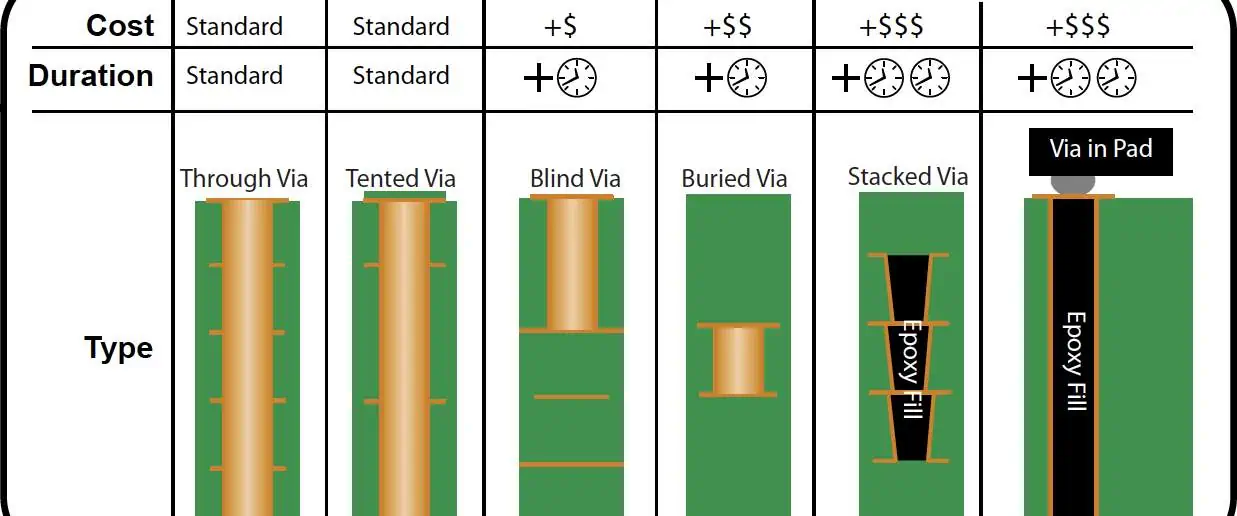
Types of RFI Shielding

FULL PCB MANUFACTURING Quote

The RF waves have the ability to impact the performance of the individual components coupled with the whole electrical system. There are different classifications of RFI based on the how severe these RFI effects are.
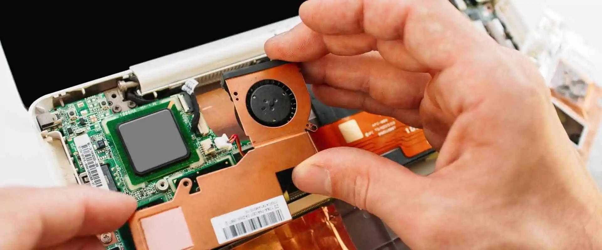
Board shielding

You can prevent the negative effects of radio frequency interference from reaching other circuits by encapsulating a part of an electronic equipment or a PCB inside the RF shield.

Component shielding

 The component shield is a type of RFI shielding that encases the component prone to RFI as well as emitting RFI.

Cable shielding

The impact of RFI in cables carrying digital or analog signals increases due to a parasitic reactance present in the high-frequency circuits. Therefore integrating RF shields present on cables is a way of reducing the RFI inside cables.

Importance of RF Interference Shielding

The best way to protect electronics from RFI is RFI shielding. Also, RF shielding prevents electronic or electrical devices from producing emissions. RF shielding protects devices from getting exposed to unwanted electromagnetic waves or radiofrequency waves. Furthermore, RF interference shields are usually constructed with metal that encloses the sensitive circuit inside. A good example of RFI shielding integrated in electronic circuits is the Faradayโ€™s. The materials for RF shield can absorb or reflect EMI radiations. Therefore, this ensures devices get protection from RFI.

Material properties like conductivity and permeability of the enclosure can change based on the RFI that needs mitigation. The type of circuit also influences the thickness and shape of the metal shield. The RF interference shield design is crucial because of the increasing market for electronic devices. Also, the high monetary losses resulting from RFI is also a cause for concern.

Transmissions between electrical or electronic devices result in unwelcome stress that may negatively affect their performance and functionality. These transmissions can jeopardize the privacy and security of the devices since their signals are open to interruption from external sources.

ย As a result of this occurrence, RF shielding in design is very important. Devices have the protective shield needed to reduce transmissions between different places. Also, this shield can prevent radio frequency interference when there is an enclosure around the application. Therefore, the environment of the application becomes safer and ensures that it functions well.

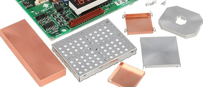
Types of Materials Used for RFI Shielding

rfi shielding materials

RFI shields donโ€™t have the same construction. This means that shields should to be custom constructed based on the electronic deviceโ€™s design and application. There are many factors to consider during the design process. These factors include material thickness, galvanic compatibility, application environment, budget, and most especially, the material itself. The choice of the material for your devices determines how the devices perform. Furthermore, the material type determines the cost of shielding.

There are majorly three types of metal commonly used by electronic engineers.  They include:

Aluminum

Aluminum is a great material suitable for a wide variety of applications since the metals feature non-ferrous properties. Also, it is widely known for its strength-to-weight ratio and high conductivity ratings. Due to these properties, this metal is highly recommended for RFI shielding. However, aluminum has some fabrication challenges, like oxidization and poor solderability.

Copper

Copper is a highly conductive material usually considered the most reliable and the best of all RFI shielding materials. This is because it attenuates magnetic and electrical waves. Also, copper is often integrated in MRI facilities and other crucial computer devices. This RFI shielding material is more expensive compared to the other shielding materials.

Pre-Tin Plated Steel

Pre-tin plated steel is a low-cost solution in cases of low frequencies in the kHz range. Also, this material provides excellent levels of corrosion protection. This helps to prevent rusting.

Common Causes of Interference

Interference results from unwanted radio frequency signals interrupting the use of electronic devices like television, cordless telephone or radio. Also, interference can prevent reception. It may result in a temporary loss of a signal, or it may impact the quality of the image or sound produced by your equipment. Transmitter interference and electrical equipment are the two most common causes of interference.

Transmitter interference

Communication systems that transfer signals that can generate interference are radio and television stations , amateur radios, and CBs. Design flaws like frayed or corroded wires, inadequate shielding, and  insufficient filtering, may make equipment prone to transmitter interference.

You can determine whether a transmitter or electrical equipment is the cause of the interference by simply unplugging one household electrical device at a time. You can isolate the source of interference through this method. Also, if your device is responding to nearby transmitters like a CB installation or an amateur radio, there will only be interference when the radio operator is talking. You might not be able to hear a clear conversation.

Electrical interference

In case of electrical interference, you may only experience frozen pictures or intermittent audio while watching over-the-air television programs. Equipment around you like doorbell transformers, smartphone chargers, hair dryers, washing machines, sewing machine, computing devices, LED lights, and clothes dryers may be responsible for this type of interference.  

Power lines can also cause electrical interference. Interference as a result of the electrical equipment of your power company is usually continuous. In this case, you must notify your power company. There is one simple way to determine the location of electrical interference. You can achieve this by integrating a small battery-powered AM radio tuned to a quiet frequency.

Applications that Require RF Shielding

rfi shielding tape

There is an increasing need for custom-made RFI shielding as consumer electronics, home appliances, and automobiles integrate built-in electronics and smart features. Also, the following systems integrate custom-made RF interference shields to protect against RFI.

5G networks

5G technology is highly susceptible to RFI. This is because the majority of these networks rely on millimeter waves. Also, the development of 5G networks has to follow EMC regulations. Also, RFI shielding is integrated to achieve electromagnetic protection.

Military systems 

Military systems integrate mission-critical data and as such any susceptibility to RF interference can make the data very prone to hackers. Furthermore, the RF interference shielding can be specially designed for military communication applications to prevent any form of data. Also, military vehicles need protection from RFI and EMU to ensure reliable and safe operation.

Automotive industry

The use of autonomous and semi-autonomous vehicles resulted in the design of several sensors and electronic components into vehicle architecture. To ensure a vehicleโ€™s safe operation, the response of these electronics systems is crucial. Also, automotive networking integrates ethernet communication protocols to create data transfers using a central computer system.

Furthermore, non-metallic body components such as bumpers or panels are prone to any external RF noises. Some RFI shielding techniques are integrated in automobiles to allow the smooth operation of electronic systems.

Medical equipment

Sophisticated medical devices and equipment integrate the principles of electromagnetics. Therefore, interference could cause any glitch which could possibly cause the loss of human life. As a result, RFI shielding is strictly integrated in medical devices. This helps to prevent the malfunctioning of these devices due to RF noises.

What is RF Shielding Effectiveness?

RF shielding effectiveness is the capability of the RF shield in attenuating an electromagnetic field. Also, the RFI shielding effectiveness can be mathematically described as a ratio between the strength of the electromagnetic field before as well as after placing RF shields. Also, it is usually expressed in dB or decibel.

Furthermore RF shielding effectiveness deals with the ratio between the magnitudes of an electric field. Also, you can determine the effectiveness of RF shielding by simply getting the ratio between the amplitudes of the magnetic field before as well as after placing an RF shield.

Furthermore, RF shields can reduce interference and shield electronic circuits. RF shields create enclosures that offer a shield between the susceptor and emitter of interference. Hence, this diminishes the strength of the electromagnetic field.

What are the factors affect the effectiveness of RF shielding?

There are several factors that affect RF shielding effectiveness. Some of these factors include:

  • The incidence electromagnetic fieldโ€™s frequency.
  • The RF shielding materialโ€™s permeability, thickness, permittivity, and conductivity.
  • The distance between the shield and the emitter of RF interference.
  • The electromagnetic field source type like the magnetic field, plane wave, or electric field.
  • The quality of bond between the surface of RF metal shields

How to Design Effective RF Shielding

There are two main purposes shielding serve. The first is to stop interference and prevent eavesdropping, wiretapping, and electronic hacking. The function of the equipment within the shield will always indicate the type of shielding needed. Sensitive equipment needs protection from a nearby ambient interference. Also, high-performance shielding is crucial.

However, you might just need minimal shielding to prevent eavesdropping on classified data on a commercial computer. There are some factors that impact the exact level of shielding required. These factors include the sensitivity of the data being processed, the distance between equipment, and the type of equipment involved.

EMI and RFI are two types of radio frequency interference. Any electromagnetic radiation frequency can produce interference. Also, RFI occurs when the electromagnetic waves are in the radio frequency part of the electromagnetic spectrum. Radio waves have frequencies that range from 3 kHZ to 300 gHZ. EMI and RFI are terms that are frequently used interchangeably, EMI is more common. In terms of radio frequency spectrum, RFI is considered a type of EMI.

Difference Between EMI and RFI

EMI and RFI are two terminologies that refer to similar phenomena. However, RFI is usually regarded as a simple subset of EMI. These two terms are usually interchangeably used, and for good reason.

Radio frequency interference (RFI) usually refers to electromagnetic fields at radio frequencies. With more concern on higher-end frequencies used in radio products (100 MHz and higher). As regards this, RFI refers to radiated emissions. This is the reason the word โ€œradioโ€ is in the acronym RFI. Furthermore, electromagnetic fields generated from some source can emit noise in a victim PCB. This could measure as a conducted current in an interconnect or a circuit.

One can say Electromagnetic interference (EMI) is a general term that could mean radiated electromagnetic fields or conducted currents from a device. As regards frequency, the term โ€œEMIโ€ could also refer to noise around the frequency domain. This includes frequencies normally related to RFI. While higher frequencies are commonly associated with radiated EMI or RFI, a device could generate or receive radiated or conducted EMI at any frequency.

Although RFI is usually considered a part of electrical noise generated by any EMI source, it also refers to currents or radiation obtained from a narrowband RF source instead from a broadband source. According to some sources, RFI ranges from several kHz to about 30 MHz. However, in the reality, it is usually around anywhere up to very high frequencies integrated in wireless products.

How to Reduce RFI in Electric Structures

The RFI signals degrade the functioning of electronic circuits and equipment. Therefore, they are undesirable.  Furthermore, they can make error rates increase and this could result in loss of data in data systems. Also, it could result in wrong measurements of electrical signals.

 Furthermore, there are some regulatory requirements that regulate the highest amount of interference emitted by electronic equipment. But, it is equally impossible to have equipment or device that is RFI-free. The best thing a designer can do is to regulate and minimize the RFI, and as such preventing it from interrupting other nearby equipment. Also, you can prevent it from interfering with equipment sharing the same power lines.

Also, it is important that manufacturers protect their equipment from the interruption emitted by other equipment or from those that are nearby. Furthermore, they should prevent the RFI or EMI emitted from their equipment, from impacting nearby device or equipment or those that share similar power system.

One of the most effective and common methods that reduce the impacts of radiated RFI is shielding. Power line filters can reduce conducted RFI. This reduces the conducted noise coming out of the equipment. Also, the line filters prevents any incoming RFI.

Using RFI filters at the input of the electronic or electrical equipment is a design method that can help to reduce incoming interference and also preventing the interference from returning to the electrical power systems via the power code. Therefore, the RFI filter comprises passive components in a pass filter arrangement. This reduces the RFI signals by trapping them and as such, preventing the signals from entering or coming out of the equipment.  

Conclusion

RF shields reduce or prevent interference and offer protection to electronic circuits. Also, RF shields create enclosures which offer protection between the susceptor and emitter of interference. Therefore, this reduces the strength of the electromagnetic field. In electronics, there are various classifications for RF interference shielding. This includes board shielding, cable shielding, and component shielding.

How Lidar Technology and PCBs Are Changing the Craft of Manufacturing

lidar technology

Printed Circuit Boards (PCBs) connect electronic components. PCBs are vital to the modern world. All electronic devices have PCBs.

A PCB is traditionally a dense and complex board with several layers. Standard PCBs have a layer of fiberglass. However, more sophisticated interconnect technology applies to PCBs.

As technology increases, so does the complexity of PCBs. This development has created new challenges for manufacturers. PCB manufacturers must keep up with industry trends.

The increasing functional complexity of devices is challenging manufacturers of PCBs. They are also experiencing challenges due to miniaturization. In addition, the growing number of components on a board leads to higher costs and lower reliability.

Lidar technology has revolutionized PCB design in several ways. It can provide more accurate measurements, faster production, and better quality.

Lidar technology is the process of using light to scan the environment. It is a popular method of surveying objects in three dimensions and can be helpful for many different purposes, such as mapping, navigation, and machine vision. Scientists working for the US military developed the first commercial Lidar system in the 1960s, which was applicable for artillery targeting and guided missile guidance.

Lidar helps PCB designers by providing them with more accurate data about the design layout. This improvement has led to a decrease in the time it takes for PCB design and an increase in efficiency.

Other industries, such as automotive manufacturing, aerospace engineering, and even architecture, have used lidar technology. In addition, Lidar systems are now helpful in many applications, including autonomous cars, drones, 3D printing, robotics, and more.

There are several different types of Lidar, such as sea-based, air-based, and ground-based. The kind used in autonomous cars is popular as laser radar.

Introduction to Lidar Technology, the Advanced Discovery and Inspection Solution for PCB Manufacturing

lidar technology PCB

Lidar is an acronym for Light Detection and Ranging. We refer to Lidar as a remote-sensing technology making use of light as a pulsed laser to measure the properties of an object. It is a technology that uses light to detect objects, measure distances, and map surfaces. Lidar measures distance through the process of illuminating laser light to objects and evaluating reflected light. The Lidar systems can also scan objects and detect environmental changes by measuring light waves that bounce off them. We sometimes call it 3D or laser scanning.

Lidar technology has been in use for decades, but its recent developments have made it more accessible to PCB manufacturing companies. The latest advancements in lidars have made it possible for companies to inspect PCBs accurately at high speed.

Lidar uses light in the near-infrared region of the spectrum (wavelengths of 0.8 to 1.3 micrometers) to create a point cloud of measurements, which can help make 3D maps of inaccessible or dangerous areas.

Lidar is helpful in many fields, including astronomy, meteorology, geology, geography, automotive, aerospace, 3D printing, and robotics. It is also applicable in autonomous navigation in self-driving cars and drones.

What is a Lidar PCB?

A lidar PCB is a printed circuit board containing a lidar sensor’s components, which is an essential part of the Lidar system.

Lidar PCBs typically consist of FR-4 glass epoxy laminate or copper-clad laminate. As a result, we can use them in all Lidar systems, such as range finders and scanners.

Lidar PCBs contain photodiodes, reflective elements, signal conditioning circuits, and amplifiers to convert light signals into electrical signals.

Using pulsed laser light, LiDAR sensors measure distances to detect objects in a range. The lidar PCB has an onboard processor that transmits and receives data. This feature allows for precise synchronization of the scanner’s movements. It also allows the computer to build a map of the area of data collection. It also includes point cloud maps, which reveal complex spatial relationships. These maps help identify objects like people, vehicles, and terrain.

PCB manufacturers have been using CO2 lasers for many years. They have shown that they are efficient in removing dielectric layers. However, they are not effective at drilling holes smaller than 75 mm.

How LiDAR works

lidar PCB

You beam light toward a target and then measure the time it will take for the light to bounce back to the source. The lidar sensor records the time and uses such data to precisely calculate the distance between itself and the object/ground. The sensor then repeats the measurements million times and transmits the obtained information to a computer system that will create the area map related to the data collection criterion.

We refer to the 3D visual representations as Point Cloud maps. They include vital components and GPS identifying the transmitted light energy’s X, Y, and Z locations. In addition, onboard computers use the 3D map of the surrounding for navigation.

The lidar sensor fires a series of pulses between 8 to 108 laser beams. Each beam pulse can transmit billions of photons within a given second. There is simultaneous processing of data points and calculations, making the Lidar highlight objects accurately, determine their shape and display how they move. A computer algorithm will then simulate and assemble the figures to form a complete picture of the thing and its surroundings.

How to Use Lidar Technology in PCB Design

Lidar is a 3D imaging technology that works like radar. However, Lidar is 1 million times faster compared to sound waves you measure using sonar. So instead, you use light pulses to create a series of points in space suitable for making high-resolution images of objects.

Lidar technology has many use cases in PCB design. For example, it can help to generate CAD models, provide accurate geometry data and enable the production of 3D printed prototypes.

Lidar is an artificial intelligence (AI) tool that allows designers and engineers to create high-resolution designs for PCBs. Lidar AI design software scans the environment and creates CAD models based on the information gathered from the scanned environment.

Benefits of Lidar

Using LiDAR to map objects and create 3D models is an excellent idea for architects, engineers, landscape designers, and many other professions. The advantages of using LiDAR include speed, low-light performance, and high resolution and accuracy.

Resolution & Accuracy

We can use LiDAR (Light Detection and Ranging) technology to capture thousands of data points and produce reliable 3D representations of objects. The data helps to provide accurate ground truth, enabling safer navigation through diverse environments. It’s also valuable for construction, oceanography, agriculture, and transportation.

LiDAR sensors can scan millions of times per second. This trait allows LiDAR technology to provide reliable ranging over short ranges. In addition, we can combine the data with other sensory data to produce precise measurements.

LiDAR systems fall into two different types. Mechanical scanning LiDARs have some shortcomings. In contrast, solid-state designs are less expensive and more user-friendly. They also provide a path to mass-market automotive LiDAR solutions.

LiDAR also has applications in forestry. It allows forest management to determine the heights of the canopy. You can use it to interpret the shape of the trees and scan areas of high-risk flood risk.

3D mapping

Using LiDAR to map the environment is an excellent way to produce accurate and reliable 3D maps. We can use these for many applications, including classification, risk assessment, and disaster response. LiDAR mapping can map entire regions and specific objects and features. For example, liDAR can effectively map buildings, trees, and waterways. It also provides positional accuracy and georeferencing for each measurement.

LiDAR systems measure the height and width of a surface by using pulses of light. A plan then uses these measurements to create 3D mapping point clouds and register them with odometry. Next, you use this data to generate a Digital Elevation Model (DEM). The DEM usually has a 3-m horizontal resolution and a vertical precision of 0.1-m.

LiDAR is an ideal choice for mapping because it is accurate, reliable, and cost-effective. It helps to map large areas quickly and accurately. You can mount its sensors on cars or airborne.

Low Light Performance

Choosing the best sensor for your application requires understanding the trade-offs involved.

A suitable sensor must distinguish between different light intensities. This feature is essential for many applications, such as machine learning models.

The best sensors have large pixels to collect more photons. Consequently, it improves the dynamic pixel range and allows for better functioning in low-lighting conditions.

The best sensors also have a low cost, which is essential in many applications. This possibility is because the silicon-manufacturing process limits the silicon area required for a device. This is why high-quality, highly integrated CMOS sensors are more than a match for traditional charge-coupled device (CCD) sensors.

Speed

Since lidar data are distance measurements you obtain directly, there is no need to interpret or decipher them. This reason makes performance to be faster and reduces the need for processing.

Why is Lidar a Game-Changing Technology in the PCB Industry?

FULL PCB MANUFACTURING Quote

Lidar is a technology that has revolutionized the PCB industry. It has enabled PCB manufacturers to produce high-quality products with increased productivity and reduced costs.

Lidar technology benefits are numerous. For example, it can help in product design, testing and inspection of the product after production, and quality control to ensure that it meets all quality standards.

Laser scanning technology is applicable in companies like Apple, Microsoft, and Amazon to create 3D models of objects from different angles and distances to facilitate their design process.

Top 3 Ways to Use Lidar Technology in PCB Production

Lidar for PCB design: This technology can suit the design of PCBs. The Lidar scans the object from different angles to provide information about its shape and size. Consequently, designers can make better decisions when designing PCBs.

Lidar for PCB manufacturing: This can help create a highly accurate digital model of an object or product before its production using 3D printing technology. The Lidar scans the thing multiple times to create the digital model, which can then be converted into a physical prototype using 3D printing technology or CAD software.

Lidar for PCB print: Some companies use lidars to produce high-quality PCBs as part of their production process. It is an advanced version of the laser scanner, and it can record a digital image of objects in the form of light/radiation emitted from lasers.

Laser scanning: Laser scanning is similar to Lidar technology as it employs lasers to take a digital image of an object or environment. Lidar and laser scanning differ because while Lidar maps out 2-D surfaces, laser scanners map out 3-D surfaces.

Other LiDAR Applications

Using LiDAR technology has the following five applications:

  1. Woodland And Agriculture

Drones using LiDAR can help survey big farms to see how we can apply resources to boost output. They may also apply to such places to build 3D models illustrating how human activity has affected forest regions. Again, LiDAR’s capacity to pierce dense vegetation is a significant benefit.

  • Land Surveying

Drones equipped with LiDAR sensors can rapidly, precisely, and affordably produce 3D digital terrain models (DTM) of difficult-to-reach places. UAVs are the best equipment for covering certain geographical regions when a human-crewed aircraft is an overkill. As opposed to helicopters or planes, drones are cheaper and faster to deploy, lowering costs and danger.

  • Maintenance-Required Power Line Inspection

Huge safety risks arise from routine maintenance of electrical lines. LiDAR technology enables the early detection of problems with electricity lines. Utility firms can immediately analyze damage using UAVs and devise the least dangerous remedy.

  • Advanced Transportation

LiDAR technology is an excellent resource for urban planners who want to increase the capacity of rail stations and mass transport networks. To develop plans for future transportation infrastructure, UAVs with LiDAR sensors can scan large regions and produce essential data.

  • Minecraft Applications

For determining material quantities in open pit mines without interfering with work happening on the ground, LiDAR proves to be a superb tool. In addition, when we include drones in mining processes, it reduces time, money, and risk exposure.

Types of LiDAR Technologies and What They Do

There are many kinds of lidar systems on the market, each with unique qualities and uses.

1. Topographic LiDAR

The most popular Lidar is topographic, which creates high-resolution digital elevation models (DEMs) of the earth’s surface. This kind of Lidar can gather data at a high resolution and measure the distance to the ground using laser pulses. Maps of landscape features, including mountains, valleys, rivers, and coastlines, are created using topographic Lidar. Additionally, it helps to create digital terrain models and orthophotos (DTMs).

2. Mobile Mapping Lidar:

 Mobile mapping lidar is a form of Lidar used to produce detailed 3D maps of a specific region. Usually installed on a vehicle, this kind of Lidar maps urban and rural areas. Applications for mobile mapping lidar include asset management, urban planning, and land surveying.

3. Airborne Lidar:

From the air, airborne Lidar helps to produce 3D maps of vast regions. Lidar can gather information over great distances and is generally part of airplanes. Applications of airborne Lidar include topography mapping, forest inventory, and archeological investigation.

4. Terrestrial Lidar:

This sort of Lidar helps to gather information from the ground. Typically installed on a tripod, this Lidar is suitable for topographical mapping features, including structures, highways, and rivers. In addition, land surveying, engineering, and archaeological investigation are a few terrestrial Lidar uses.

5. Scanning Lidar:

This Lidar helps to produce 3D maps of a specific area. This kind of Lidar scans a space in a spiral or raster pattern and is often part of a tripod. Applications for scanning lidar include 3D modeling, archeological investigation, and 3D printing.

6. Multi-beam Lidar:

This kind of Lidar helps to gather information from several laser beams. This kind of Lidar can concurrently collect data from several directions and is common in an airplane. There are several uses for multi-beam lidar, including 3D mapping, terrain modeling, and imaging.

7. Waveform Lidar:

This sort of Lidar helps to gather information from several laser beams. Lidar is suitable for many different purposes, including 3D mapping, terrain modeling, and imaging. It may concurrently collect data from numerous directions. For example, waveform lidar can easily determine the laser pulse strength and precise distance to a target.

8. Geodetic Lidar:

This form of Lidar helps to gather data over long distances. Applications for this kind of Lidar include asset management, engineering, and terrain mapping. For example, it is common in airplanes. Geodetic Lidar helps to create high-resolution DEMs and DTMs and can gather data across great distances.

9. Laser Scanning Microscopy Lidar:

This kind of Lidar helps to gather information from tiny things. Applications for this kind of Lidar include 3D modeling, 3D printing, and medical imaging. High-resolution 3D representations of small objects are easy to produce using laser scanning microscopy or Lidar.

10. LiDAR-based Photogrammetry:

We can gather data from aerial photographs using a Lidar called photogrammetry based on Lidar. Applications for this kind of Lidar include asset management, digital terrain modeling, and terrain mapping. Engineers create high-resolution DEMs and DTMs using LiDAR-based photogrammetry.

What Benefits Does Lidar Technology Have for PCB Manufacturing?

LidaR PCBA Board

1. Increased Accuracy and Precision

The most significant benefit of lidar technology in PCB fabrication is greater precision and accuracy. Manufacturers can verify that each element is present by utilizing laser light to measure the distances between components. This check is crucial for complicated PCB designs because even the slightest misalignment might fail the entire board. In addition, Lidar can detect short circuits and verify that the PCB is adequately insulated.

2. Accelerating the manufacturing process

Additionally, the utilization of lidar technology significantly decreases the time required for PCB fabrication. Manual measurements are time-consuming and prone to human mistakes, whereas Lidar can finish the entire operation in a fraction of the time. This speed expedites manufacturing, resulting in potential cost savings for producers.

3. Cost Savings

Using lidar technology decreases costs in two ways: first, it reduces the time spent on production, hence decreasing labor costs; second, it helps to guarantee that PCBs are manufactured correctly, thereby eliminating the need for costly rework and repairs.

4. Enhanced Safety 

Increased safety The use of lidar technology in PCB fabrication also boosts security. This removes the need for unsafe manual measurements that expose personnel to toxic chemicals. Additionally, Lidar may detect short circuits, which can cause significant harm if not discovered.

5. Environmental Impact Reduction

Lastly, applying lidar technology can lessen the environmental effect of PCB production. This is because the technology helps verify that all components are appropriately positioned, eliminating the need for rework, which may produce toxic emissions and waste.

What The Future Holds for LiDAR Technology in Printed Circuit Board (PCB) Manufacturing

In the PCB manufacturing sector, LiDAR (Light Detection and Ranging) technology is a fast-growing field. It can swiftly scan and measure distances, and its use in PCB creation and testing is rising. The technique has simplified production procedures and increased the accuracy and speed of PCB manufacturing.

In PCB manufacturing, manufacturers measure the size and form of a PCB before its fabrication. As a result, manufacturers can produce PCBs that fit the customer’s exact requirements.

In recent years, the usage of LiDAR technology in PCB manufacture has increased significantly since LiDAR offers several benefits over conventional PCB production processes. For example, it can scan and measure the precise size and form of a PCB in a considerably shorter length of time, which cuts production costs and improves productivity. It also enables the development of exact and accurate printed circuit boards, which enhances product performance and dependability.

Quality monitoring & inspection

LiDAR is useful for PCB production quality monitoring and inspection. The technique precisely and rapidly finds PCB faults, saving time and money in the long run. Additionally, it discovers and identifies design defects in PCBs, minimizing production mistakes and ensuring that the finished product fulfills client requirements.

Improved productivity

We anticipate that LiDAR technology will continue to expand in PCB manufacturing as manufacturers attempt to decrease costs and boost productivity. In the future, LiDAR may assist in automating the PCB creation process, substantially cutting the cost and time necessary to produce a PCB. In addition, LiDAR might aid in constructing highly accurate 3D representations of printed circuit boards (PCBs), which could facilitate virtual testing and prototyping.

Complex products

LiDAR might aid manufacturers in the production of PCBs with greater degrees of complexity. Therefore, it might enable manufacturers to produce PCBs with sophisticated features, like as integrated circuits, that are challenging to create using conventional methods. In addition, LiDAR can assist the fabrication of very accurate PCBs with several layers, which is suitable for applications such as smart gadgets and wearables.

LiDAR technology can change the PCB manufacturing process as a whole. It can decrease manufacturing processes’ complexity and improve PCB fabrication’s precision and speed. In addition, it might enable manufacturers to produce more sophisticated and accurate PCBs, enabling the development of several new applications and industries. As LiDAR technology continues to advance, we anticipate it will significantly influence the PCB manufacturing business.

Conclusion: Use the Future-Proofing Technology of Laser Scanners in Your Next PCB Production Run

Lidar uses time-of-flight measurements to create 3D representations of objects and scenes from data collected by scanning laser beams directed at targets.

We can use Lidar to distinguish between different materials and detect various types of radiation (such as infrared and ultraviolet). Moreover, we can measure atmospheric constituents such as temperature and humidity, map terrain elevation, estimate population density, and track moving objects such as vehicles.

Finally, LIDAR systems produce three-dimensional point cloud data that we can use for various applications, including mining site mapping; construction project planning; environmental monitoring; automotive design; robotics and autonomous systems; and navigation. Contact our company to get solutions to your PCB needs using lidar technology.

How to Improve Industrial Control by New PCB Technology

Industrial Control PCB

We live in an era where technology is taking over every existing industry. From the academic industry via online classes to the health sector via health monitoring apps. However, the sector that has most probably gained the most infiltration by technology is the manufacturing industry. In the 21st century, almost every production process must utilize technology to get the manufacturing procedure right. That is where ICS (industrial control systems) come into the picture.

Many distinct types of Industrial control systems have been deployed in many different sectors. Using some Industrial control system along with related processes and equipment is necessary for practically all essential infrastructure, industrial production areas, power management, transportation, and water treatment. However, even though these ICS applications are very useful in production, they must run on a complex PCB to function appropriately and increase efficiency and productivity. Moreover, using them in a production process is a pretty complex task. However, are there manufacturers who have mastered the skill of using ICS in the production process of their products?

Industrial control Systems in a Nutshell

Industrial Control

The term Industrial control system (ICS) refers to various CS (control systems) plus related instruments, including equipment, control, systems, and networks needed to automate and operate industrial processes. Every ICS works differently and is designed to effectively handle duties electronically depending on a couple of factors, such as the industry in which you are using it. However, today almost all industrial sectors use the equipment and procedures in an industrial control system.

Industrial control is the automation of manufacturing, mining, and power systems to increase production rates, improve product quality and reliability, or optimizing resource use.

Industrial control systems are the backbone of many industries. They are useful in all industry sectors, from manufacturing to power generation and distribution. Industrial automation is a subset of industrial control that mainly involves automating industrial processes such as material handling (e.g., palletizing), assembly lines, machining operations and packaging.

Digital process automation (DPA) is an emerging technology that promises to automate more complicated tasks in industry by using software agents that can monitor and adjust processes based on changing conditions.

There are a couple of ICS kinds. However, the Distributed Control system, supervisory control, and data acquisition are the most popular in the market. In addition, field Devices, which take supervision orders from distant stations, frequently manage local activities.

Supervisory control and Data Acquisition (SCADA)

A system like SCADA cannot offer total control. However, it concentrates on providing supervisory-level control by utilizing its capabilities. Moreover, supervisory control and data acquisition systems have components dispersed over several places, most often PLC (programmable logic controllers) and other commercial modules. An HMI (human interface machine) connected with a SCADA system allows for centralized control and monitoring of various process outputs and inputs as well as the acquisition and transmission of data.

SCADA is used chiefly for remote management and monitoring of field sites via a centralized control system. SCADA systems can automate this process efficiently so that employees are not required to travel significant distances to complete tasks or collect data. The closing and opening of breakers and valves, environmental monitoring, and data collection from a sensor system are all controlled locally by field devices.

Supervisory control and data acquisition systems are primarily good in industries that involve electrical power distribution and transmission, water treatment and distribution centers, and pipeline control and monitoring.

Distributed Control Systems

FULL PCB MANUFACTURING Quote

DCS is a system that technicians utilize to manage manufacturing equipment kept in one place. In a distributed control system, communication to set points is via the system’s controller, which can then tell actuators or even valves to function in a specific way that will maintain the intended set point. Moreover, data collected in the field can be utilized for straightforward process control, archived for future utilization, or even combined with information from other parts of the system’s plant to create sophisticated control plans.

Every DCS controls several devices or controllers that are components of the whole manufacturing process using a looped supervisory control that is centralized. By using this technology, industries now have instant access to information on operations and manufacturing. Moreover, a DCS can lessen the effect of “single faults” on the entire system by utilizing multiple devices during manufacturing.

DCS systems have multiple applications in sectors such as:

  • Wastewater treatment
  • Oil and water refineries
  • Chemical manufacturing
  • Electrical power generation
  • Manufacturing

Actual ICS Implementation

ICS environments implementation mainly uses a combination of SCADA and DCS that incorporates features from these two systems.

Vital Components of an ICS Environment

The software and hardware systems that efficiently monitor and manage actual physical gadgets in the field tend to be operational technology or OT variables. Moreover, every industry has different OT duties. OT devices include, for instance, equipment that measures temp in industrial settings.

Remote Terminal Unit

A remote terminal is an efficient field gadget that bears a microprocessor. The microprocessor receives instructions and relays data to the MTU.

Control loop

Hardware components like actuators and PLCs are a part of every CL (Control Loop). The CL interprets signals from motors, switches, breakers, control valves, sensors, and other devices like these. Moreover, the controller will use the variables that these sensors have measured to handle jobs or finish processes efficiently.

Human-machine Interface

A GUI (graphical user interface) program enables the communication between the human operator and controller hardware. Additionally, it may provide previous data acquired via the gadgets in the industrial control system environment and status information. Moreover, technicians use it to construct and modify parameters in the configured set point, control algorithm, and controllers.

Remote Maintenance and Diagnostics

Remote maintenance and diagnostics refer to recognizing, stopping, and recovering from unusual operations and failures.

Control Server

Lower-level (LL) control gadgets receive communication with control servers which also host the PLC or DCS supervisory control programs.

Master Terminal unit or SCADA

The SCADA gadget also sends instructions to out-of-band RTUs.

Intelligent Electronic Devices

An IED is an intelligent gadget that can gather data, exchange messages with other smart gadgets, and carry out local control and processing. Auto local level (LL) controls are made possible by employing intelligent electronic devices in control systems such as DCS and SCADA.

Data Historian

Data historians are centralized databases that record all process information in an Industrial control system environment before exporting this information to the company’s information system (IS). The knowledge acquired is subsequently put to use for EL (enterprise-level) planning, process analysis, and statistical process control.

What exactly is an Industrial Control System?

INDUSTRIAL Control PCBA

SCADA systems undertake several functions which permit proper remote facilities management. Here are the main functions of SCADA systems.

Data Acquisition

Technicians use analog to digital conversions in the collecting of SCADA information. Moreover, technicians utilize varying degrees Celsius to express temperature when dealing with SCADA systems.

A SCADA system converts the transmit signal intensity to dBm. Moreover, errored seconds serve as a type of measure of channel quality.

Network Data Communication

The gathered data moves to a master consolidator on its initiative or as a response to data requests.

Analog (T202, POTS) or digital (RS485, TC/IP) communication channels are possible in network data communication. Moreover, in addition to any content certification, the architecture of SCADA networks often includes some form of transit validation.

Data Presentation

There is need to organize and process collected data and then present for the system operator to make the correct control decision and response. Moreover, the presentation might vary from a simple tabular presentation encompassing logged events to a complex graphical presentation.

Control

If the systems support outputs and the control decision is warranted, technicians can dispatch appropriate commands to specific configurations or operational changes. Most control actions tend to be undertaken by PLCs and RTUs.

Communication within Industrial Control Systems

Control modules and devices use communication protocols in industrial control systems to communicate information. Moreover, various industrial control systems settings employ a variety of communication methods. Most of these system protocols were created for particular uses, including the automation of processes, power systems and structures, and many other things. Moreover, the development of these efficient protocols guarantees compatibility across various manufacturers. Specific protocols, however, can only be used with equipment made by the same industrial manufacturer. The most utilized Industrial control systems protocols include:

Ethernet for Control Automaton Technology (EtherCAT)

An open-source, free-to-use communication protocol that uses Ethernet technology in industrial settings. EtherCAT helps in the application that involves automation with a jitter of one second and short update cycles (around 100 seconds).

Common Industrial Protocols (CIP)

Services and messages for configuration, synchronization, security, control, and other purposes make up a CIP. Moreover, you can combine the internet and Ethernet network with the ICP for better functionality. Numerous CIP modifications offer intercommunication and integration for various network types.

Building Control and Automation Networks

Fire detection, building access, lighting, air conditioning, ventilation, and heating are all controlled by this protocol.

Open Platform communication (OPC)

For industrial communication, there are several specifications and standards known as OPC. Microsoft created these technologies long ago to cater to windows OS (operating system). They are the foundation of the Open Platform communication standard (DCOM, COM, and OLE).

Modbus

The Modbus system protocol is one of the first industrial control system protocols introduced to the industry in 1979. Modbus is the standard communication protocol in most, if not all, ICS settings, and it employs serial connections with PLCs. The serial Modbus that transmits data using the HDLC (high-level data link control) standard and the Modbus-TCP that transmits data using the TCP/IP system protocol are the two different types of Modbus protocol implementation.

Distributed Network Protocol

The DNP protocol operates across three layers – the transport, application, and connection. As a result, the DNP approach is frequently applicable in water and water-waste treatment facilities.

Process Field Bus

During field operations, PROFIBUS employs RTU to RTU, MTU to MTU, and RTU to MTU communications. Moreover, there are only two options:

  • The Profibus PA, which is short for Process Automation) โ€“ it efficiently monitors the measuring equipment through the process control (PC) system.
  • Profibus DP, which is short for decentralized peripherals โ€“ Controls actuators and control sensors through central controllers.

Most common Threats to ICS

Every ICS continuously integrates new applications and tech in OT and IT to enhance system functionality and productivity. However, because OT and IT are now part of ICS, fraudsters may attack them more easily. One of their prevalent weaknesses is the lack of security solutions utilized in the OT infrastructure to secure legacy control (LC) systems like SCADA. Additionally, businesses must deal with the growing security issues in cutting-edge technologies like cloud computing, IoT, and big data analytics. Moreover, Centralization exposes previously undiscovered weaknesses in the cyber ecosystem.

Most attacks against industrial control systems are frequently focused attacks that leverage the entry point provided by the industrial control system to obtain access to the system and migrate inside the company. The Stuxnet virus, which hackers used to control centrifuges within Iranian nuclear facilities, plus the BlackEnergy, which harmed Ukrainian power generating facilities, are just two examples of how infiltration occurs to ICS systems. Even though most assaults concentrate on industrial espionage and data theft, the two examples above show how malware might have a kinetic impact.

The mining sector has become an excellent target for hackers looking for cyber espionage activities. These cyber espionage operations aim to gather the most recent technological intelligence and information to support particular interest groups’ growth and competitive advantage.

Examples of how ICS Works in the PCB Industry

PCBs in a Nutshell

Printed Circuit Boards are sheets of insulating material, for example, fiberglass, with tracks or metallic circuits etched or printed on it to generate electrical conductivity. Printed Circuit Boards are in almost every electronic gadget you come across, ranging from keyboards to laptops, computers, TVs, Tablets, mobile phones, and more. ICS apply in the production of PCBs due to the need for accuracy and precision.

Printed Circuit Board Assembly

Printed Circuit Boards have one main objective, to transmit electrical current to various components on the circuit board. However, for this to happen, components must be mounted on the board through a process known as PCB assembly. During this process, technicians utilize SMT (surface mount technology), which requires the utilization of ICS to get right.

After soldering every electrical component, the board can function accordingly.

Materials that make up a Printed Circuit Board

You can manufacture the base or core of a printed circuit board using different materials. The only catch when it comes to choosing the base components is that the element should be:

  • Durable
  • Insulating
  • Heat resistant

These requirements show up because printed circuit boards are utilized primarily on harsh environments and must endure high heat levels.

The most common materials that technicians utilize to manufacture printed circuit boards include:

  • Ceramic
  • Resin coated copper
  • Non-woven glass plus epoxy
  • Cotton paper, epoxy, and phenolic cotton paper

Types of Printed Circuit Boards

Printed circuit boards come in many variations according to how the manufacturer produces them. These variations include:

  • Rigid-flex printed circuit boards or rigid, flexible printed circuit boards
  • Flexible or flex-printed circuit boards
  • Rigid printed circuit boards
  • Multi-layer printed circuit boards
  • Double-layer or double-sided printed circuit boards
  • Single-layer or single-sided printed circuit boards

Printed Circuit Boards Manufacturers

Many different printed circuit board manufacturers exist across the globe. Most of them reside in China and the USA. However, only some PCB manufacturers have the technology and the capability to handle ICS PCB production. However, companies like Rayming have the ability and technology to efficiently utilize ICS to generate PCBs.

Rayming PCB

Rayming is a china based Printed Circuit Board assembly company that utilizes ICS to offers complete circuit board assembly services. Moreover, regarding PCB production, Rayming is one of the world-leading printed circuit board assembly and manufacturing companies. The company came into the limelight in 2005 and has been operational since then, providing quality products every time. Through these years, Rayming has mastered the skill of using Industrial control to produce Printed Circuit Boards more efficiently.

Services offered in Rayming

Rayming specializes in offering the following services to companies worldwide:

  • High-quality printed circuit board fabrication
  • Printed circuit board assembly
  • Component sourcing services

Moreover, Rayming also offers services in high-end PCBs, for example, flex-rigid printed circuit boards, aluminum printed circuit boards, HDI boards, high-frequency circuit boards, Teflon PCBs, and Rogerโ€™s PCBs. Using tech and ICS, Rayming can produce quality circuit boards each time.

Moreover, Rayming offers partial turnkey and complete turnkey PCB assembly services to produce all circuit boards. For complete turnkey PCB assembly, Rayming handles the entire manufacturing process of the PCB, which includes:

  • Manufacturing the PCB
  • Procuring production components
  • Testing the PCB
  • Continuously monitoring the PCB to check on the quality of the circuit board.
  • Final assembly

Moreover, Rayming has been in the industry for over 15 years. Therefore their procuring abilities are top-notch. Furthermore, they only purchase original components; therefore, you can be sure that your PCB will be high quality. And since quality is a significant aspect to consider when dealing with PCBs, they deliver the best circuit board you can find in the market.

PCB Assembly Process followed by Rayming to generate the best PCBs via ICS

For printed circuit board production Rayming utilizes both manual and automated techniques. Moreover, while using THT component placements, Rayming places the components manually on the board. However, while employing SMT, technicians effectively use pick-and-place gadgets to locate and place components on a Printed Circuit Board.

Soldering

As per soldering, the Rayming team utilizes wave-soldering to undertake THT PCB assembly. However, when undertaking Surface Mount PCB placements, technicians use reflow soldering, which requires the utilization of ICS.

When carrying out THT PCB assembly, technicians manually place components on a circuit board. They then use wave soldering to solder the components on the PCB effectively. However, when it comes to SMT PCB assembly, technicians apply the solder paste using a solder stencil on the circuit board. After this happens, technicians place the parts on pads and then pass the board in a unique reflow oven, which melts down the solder. Additionally, PCBs with hybrid technology is wave soldered and reflowed.

Cleaning the Printed Circuit Board

After the soldering process is complete, the Rayming staff utilizes gadgets to clean the PCB and eliminate any contaminants. Technicians in Rayming thoroughly clean the constructed circuit board using the most recent method to eliminate any flux residue. Additionally multiple methods โ€“ which often combine cleaning chemicals, agitation, and heat- are employed to remove flux. After that, a thorough inspection of the PCB is performed to verify the precise component arrangement via ICS gadgets.

Inspection

At Rayming, specialists utilize high-tech inspection tools to check the quality of the Printed Circuit Board. Some techniques used by technicians to carry out PCB inspection include:

After thorough PCB quality testing, technicians deliver the Printed Circuit Board to the customer.

Delivery

Rayming delivers Printed Circuit Boards assembled via their corporation to any country via courier. Therefore you do not have to worry about order shipment. Moreover, Rayming ensures the circuit board shipment is successfully delivered at any location within an acceptable TT (turnaround time).

Benefits of working with ICS

Increased Safety and Health

Manufacturers who work with ICS enjoy one primary benefit, increased safety and health for their employees. That is because while utilizing ICS, manufacturers understand various environments before they dispatch workers to that location. Doing so helps keep the workers safe while carrying out multiple tasks.

Minimization of Harmful Exposure

The next benefit manufacturers enjoy while working with ICS is the ability to efficiently minimize and control exposure or threats created by faults or failures.

Whenever a power line fails, a SCADA or ICS system detects the failure and then alerts technicians earlier, before they arrive at the location. Doing so helps save employees from exposure that could harm them.

Protecting Assets

Through using ICS, manufacturers can easily protect their assets via the prevention technique. For example, whenever an ICS detects a fault, it alerts technicians, and then they can secure the assets around that fault before the situation escalates.

Conclusion

Industrial Control systems are, without a doubt, crucial to the manufacturing industry. Without these systems, mass production could be tricky to accomplish. However, the production of PCBs via the utilization of ICS can be a complicated task to accomplish. However, Rayming can make this possible through high-tech gadgets and highly skilled technicians. Therefore, if you have a project requiring such services, Rayming might help you.

Top 3 Electronics Panel Board Manufacturers

Electronics panel board manufacturers

The foundation of any industrial system is its cabinet design and control panel. They provide a centralized interface for operating and monitoring all relevant machinery. High electrical circuits and precisely built control circuitry send signals. It ensures the proper functioning of your machinery or equipment. The equipment is typically found in electronic control panels.

There is no mains electricity available in the electronic control panels. Also missing is any form of restricted machinery. Instead, depending on the context, the panel can be attached to a subpanel, an enclosure, or a rear panel.

Importance Of Electrical control panels

OEMs play a crucial role in the electrification of industry. The electric panel boards improve the efficiency of your electrical system. Short circuit and overload protection is provided by the essential relays. The relays are installable in these distribution boards.

In addition, OEMs are sheet metal enclosures. On the panel’s front, they display vital parameters. Vital parameters include power factor, voltage, frequency, and current. In addition, these boards can aid in regulating the supply of electricity. The supply regulates via switches and circuit breakers.

3 Best Electronics Panel Board Manufacturers

Rotation Panelization

Lighting, radios, and a selected group of low-energy appliances accounted for most of the typical homes’ electricity use prior to the advent of modern electronics. Most residences had fuse boxes, and these were adequate for typical use. The power needs of modern households have increased. This is because of the proliferation of electronic gadgets. Laptops, personal computers, and gaming systems are a few examples. Fuse boxes were replaced by electrical panels, which grew in size and capacity over time.

Electrical panel manufacturers provide products, electrical components, and electrical systems with ratings from hundred to four hundred amperes. It serves not only residential but also property owners. Electrical panel upgrades from sixty or hundred amperes to two hundred amperes capacities. These capacities are common as the electrical demands of modern households increase.

Whether you’re doing some remodeling or starting from scratch, it is always good to know what kinds of electrical panels are available and which ones are the best. Of course, you ought to learn your appliances and gadgets inside and out. It will give a good idea of how they function in order to choose the correct size for your home. So, brand recognition isn’t the only thing that matters.

When looking for a new switchboard or electrical panel board, there are some factors to consider before settling on a specific brand.

  • Location:

This is crucial as not all panels are resistant to substance penetrating or weather conditions.

  • Power requirements:

Knowing your own power needs is important before purchasing a property. Since even though most newer houses have two hundred amperes panels, that may not be enough for you.

  • Safety controls:

For the sake of your family’s safety, nevertheless, you should verify that your solar panel has adequate ability to withstand power surges, short circuits, and other electrical hazards.

  • Breaker Types and machine control:

You should look for high-quality materials and construction, not just top-tier electrical panels.

1.    Siemens Electrical Panels

FULL PCB MANUFACTURING Quote

Breaker panels from Siemens’ housing line are among the best on the market. The majority of today’s models are not only user-friendly. But also come with all the extras you’ll need to set them up. Siemens has a wide variety of panel types and sizes to choose from. So, it should be easy to find one that will work in your home.

Depending on your requirements, you can choose from panels with hundred to two-hundred amperes. The P1224L1125CU Load Facility could be an acceptable middle ground if you do not need the maximum capacity of the range but worry that a hundred amperes won’t be enough. It can handle 125 amperes and has room for 24 separate circuits.

A metal bus, which is both corrosion-proof and highly efficient, is used to power the panel’s circuit breakers. Siemens’ “instant-wire” technology is used for the neutral and ground bars. It makes the latter capable of accepting cables and shortening the installation process.

Many licensed electricians will tell you that Siemens is the best brand of the electrical panel. Many families favor these panels due to their adaptability, the excellent quality of the substances used, and the power and longevity of the panels themselves.

2.    Square D Electrical Panels

When it comes to electrical panels, Square D is the brand by Schneider Electric. It is best for producing reliable goods. The panels’ heavy steel construction makes them exceptionally sturdy. In addition, they stock a variety of panels, from the sub-panel-sized to the 200 amperes variety.

The main circuit breaker and up to five double-pole or ten single-pole breakers can be installed into the six available spaces on standard Square D 100 amperes panels. They can also serve as supplemental display areas. They are sufficient for most one- and two-bedroom apartments and smaller houses. In either a flush or surface mount configuration, they’re easy to set up.

Another of their hundred and twenty-five-ampere panels would be a good fit for a larger home. With room for twelve breakers, these are expandable in the future if necessary. The breaker panel’s twenty-four available circuits are sufficient for many houses of average size.

The Square D HOM4080M200PQCVP, a 200-ampere panel, is an alternative if you have a particularly large home or a lot of electrically demanding appliances. With its Qwik-Grip feature, the cable is insertable with little effort into the hole, and the shield can snap shut around the branch cable in seconds. As a result, the panel can do without steek knockouts and cable connectors. It supports 120/240 AC voltage with full-size breakers and tandem. Three single-pole twenty-ampere breakers and two double-pole thirty-ampere breakers are available in the panel.

3.    Leviton Panels

pcba box build assembly

The panel surge suppressor included with Leviton distribution boards is a major benefit. This safeguards not only your electronics but also your pump and motor appliances. For example, it protects the washing machine and the dishwasher from surges. Surges are sudden and dangerous voltage spikes.

Leviton also provides up to 25,000 dollars in coverage for attached indoor home devices and appliances in the event that the surge suppressor fails under normal use, which is yet another reason to consider installing one of their panels. That is undeniable evidence that they are confident in their products.

In terms of safety, the panels go above and above the UL Standards by including features like ground-fault circuit interrupter protection, which disables the panel entirely if a ground fault occurs. Sleek in appearance, they feature a white interior box with the option of an observation period. Smart Breakers is an available upgrade that provides further insight into power consumption, and their LED screening tests are easy to understand.

Breakers of two different types, thermal and hydraulic magnetic, are available for the Leviton panels. The primary distinction between the two is how the panel responds to an overload, though other factors, such as the installation site, also play a role. Thermal breakers are ideal for use in temperate indoor settings, while hydraulic breakers excel in extreme conditions.

Why Are Aerospace Electronics Manufacturers Important?

Aerospace Electronics Manufacturers

During manufacturing, aerospace electronics demand top-tier expertise because the systems must deliver outstanding performances and work perfectly under all circumstances. As a result, an experienced team of aerospace electronics manufacturers is available to ensure the aerospace industry has the best electronics.

For instance, some of NASA’s largest contractors rely on aerospace electronics manufacturers to provide the best aerospace products. This solidifies how essential aerospace manufacturers are to the aerospace industry.

Who Are Aerospace Electronics Manufacturers?

Aerospace electronics manufacturers are professionals that handle the design and installation of electronic devices and systems on aircraft and spacecraft. Aerospace electronics manufacturers serve the defense company and commercial aviation industries by manufacturing various aerospace electronics products.

From highly sensitive precision guidance and defensive systems to engine control and fuel system, communication, navigation, radar systems, and various flight controls, aerospace electronics provide comprehensive design, manufacturing, supply chain, and fulfillment services. They proffer the best practices for onboard component selection, board fabrication, material and something acquisition, assemblage, and installation.

Importance of Aerospace Electronics Manufacturers

Aerospace Electronics
  • Aerospace experts are crucial to manufacturing products, solutions, and systems that make humans travel faster worldwide or get more advanced equipment to get to space and control their activities there.
  • They help develop new solutions and technologies and support aviation, defense systems, automotive spaceships, and satellite partner industries.
  • Aerospace experts continue to help the aerospace industry by improving project production efficiency and ensuring all electronics and solutions are tested and ready for use. As a partner, they also oversee the control of delivery services of automotive parts to the market and other places of control.

Services Offered By Aerospace Electronics Manufacturers

Aerospace electronic manufacturing services include

  • ISO compliant
  • Box and panel build
  • Wire harnesses
  • Flex Circuits
  • IMSE
  • PCBA (Printed circuit board assembly)
  • PCBC (Printed circuit board component kitting)
  • Wiring modification
  • Wiring components

Advantages of An Aerospace Electronics Manufacturer

The advantages of an aerospace electronics manufacturer to the aviation industry include designing, manufacturing, prototyping, testing, quality monitoring, cable assembly, wire harness assembly, and full panel and enclosure assembly of all electronics. They also provide a quick turnaround, troubleshooting, and excellent communication to the industry.

What Are the Requirements In the Aerospace Sector?

FULL PCB MANUFACTURING Quote

The aerospace market has some of the most strict requirements and requires one of the most stringent adherence to standards compared to other sectors. Every project or technology used in many facilities is screened based on the capabilities they are to deliver. As a result, keeping up with the industry’s constantly changing conditions and capabilities can be challenging.

However, an aerospace electronics manufacturer has the resources and knowledge to cater to the manufacturing and quality demands of the aerospace and defense industry.

Role of Aerospace Electronics In the Industry

In the aerospace industry, there are various roles that electronics and the expertise of the manufacturer of such play to ensure the reliability of the process both at testing and eventual use in the company by customers or a trusted partner, and they include:

โ— Communication

Communication is essential for every contract manufacturer who engages in environmental testing, and you need someone with extensive experience. Additionally, it aids in the efficient transmission of radio signals. Without aerospace electronic products and compliance with the rigorous requirements, communication is impossible since the electronics contain PCB and other parts that help grab the signal and deliver it back to make touch with others.

However, it is not enough to have communication; quality and reliability are key to facilitating the process.

โ— Power supply

Whether it is a commercial aircraft, military aircraft, spaceship, satellite, or other mass production processes, they require adequate power. Without power, the equipment in the aircraft won’t work. Also, having the right voltage and power intensity is essential to ensure the smooth travel of the aircraft.

This aspect of an aerospace electronics manufacturer is essential to different facilities and their capabilities. They ensure each aircraft has the correct distribution of current/voltage and energy conversion.

โ— Thermal considerations

Aircraft or other space systems require thermal considerations because they perform under extreme conditions, which may include extreme heat. Since the air or space environment is not similar to earth’s, the aircraft or spacecraft product introduction needs electronics with high reliability that can help keep and regulate the external temperatures outside the system.

That way, coupled with conformal coating, there are no internal outcomes with any sub-assembly due to the external temperature.

โ— Navigation

A navigation system helps aircraft and spaceships navigate while flying and traveling around space. The navigation system is essential to aircraft, satellites, or spaceships. So, how will they work without electronics?

Therefore, aerospace electronics help the aerospace system function accordingly during the whole navigation system.

โ— Fuel conservation

In conserving fuel, electronics play an extremely vital part. It monitors and controls the temperature level around the fuel to preserve them.

โ— Vibration and shock safety

Often, when a spaceship is launched, force shock or vibrations occur, which can be harmful without a proper system that can help in controlling it.

As a result, aerospace electronics protect a spacecraft against vibrations and shock. If there is an addition of electronics, the aerospace systems can bear any shock or vibrations.

โ— Structural integrity

Electronics play a significant role in the structural integrity of aerospace systems. For instance, if sudden changes occur in the environment that result in an alteration, the electronics will make you aware of any alterations or breakdowns in the spacecraft.

This, therefore, helps in the structural integrity of spaceships and satellites.

Electronic Components for the Aerospace and Defense Industry

Aerospace manufacturers manufacture quality electronics with the most rigorous standards to withstand the extreme temperature, vibrations, shock, and altitudes associated with high-flying operations.

From communication system devices to barrier terminal blocks, the components are designed to help the aerospace and defense industry take flights to new heights and directions and land perfectly.

Aerospace Electronics Contract Manufacturing Services

Many companies specializing in manufacturing services participate in aerospace electronics contract manufacturing projects such as aerospace contract machining. They do this because of their cheap production costs and safety. The manufactured products and technology are then sent to the appropriate facilities or sector to be used for the project or support it is needed for.

Also, getting an aerospace electronics manufacturing company is easier and cheaper than building or training a new team. Best of all, contract manufacturing in the aerospace sector offers fully functional turnkey systems.

How Much Do Aerospace Electronics Engineers Earn?

It can be difficult for aerospace engineering, supply chain management, and manufacturing services of a quality management system, but it pays well. The demand for aerospace defense engineers and manufacturing services is always high. According to a source, aerospace defense engineers make an average salary of $107,800 annually.

Conclusion

The aerospace defense industry demands extra quality for all its products. This is due to the extreme conditions to which the products are exposed. As a result, skilled aerospace defense engineers who can provide safe manufacturing services are the best option.

What Is A Prototype PCB Service & Its Advantages?

Shengyi S1600 pcb

Before beginning complete PCB fabrication, it is necessary to verify the board’s functionality. Printed circuit boards (PCBs) are the backbone of the electronics industry. The complete electronics circuitry becomes defective due to a single bad circuit board. Finding this problem in multiple freshly made PCBs would be disastrous.

Miniscule and unseen flaws have a significant impact on the final PCB’s functionality. Thus, engineers require PCB prototypes before committing to mass production. If you want to be sure your design works, testing a PCB in advance is the way to go. In this piece, we’ll review in greater detail why and how this matters for your PCB layout.

What is a Prototype Printed Circuit Boards Assembly?

This phase of rapid PCB assembly prototyping is experimental in nature. In addition, this is a test run for mass production of printed circuit boards. It guarantees that the board thickness and other things get tested before going into the finished product. Errors are reducible, and thus PCB designs are more reliable results.

In addition, this facilitates manufacturers in assessing the usefulness of their planned PCBs. Also, prototype PCBs can be useful as a basis for subsequent revisions. Not included in the real PCB production method. Important prototype assemblies have both through-hole components and surface mounting.

Before integrating it into the finished product, checks your PCB. To make sure your idea works, this PCB design can be useful as a test board. It also includes building the prototype printed circuit board. Assembly of printed circuit boards allows for the detection and correction of flaws. To ensure the proper operation of the circuit. This construction requires the fabrication of a circuit board.

Numerous prototypical variations exist. Examples of these are a working model, a feasibility study, and a working prototype. Only the physical characteristics of a printed circuit board layout are shown in the graphical representation. The utility of a design can be accurately envisioned using a working prototype. The working prototype demonstrates the basic idea behind your intricate ideas.

Different Kinds of PCB Prototypes

nanya-pcb-material

Several PCB boards may be required, depending on the stage of development and the particulars of the design. Moreover, different testing methods are needed at different phases. Here are a few illustrations:

  • Visual Modeling:

ย A vital part of any printed circuit board process, visual modeling depicts the final form and function of the board. Because nothing exists in physical form yet, this is more of a proof-of-concept than a practical test.

  • Proof of Concept or Gerber files

Every printed circuit board (PCB) layout has one main objective it aims to realize. The prototype serves as proof of concept. It focuses on the core functionality of the eventual product. Simply said, it’s a demonstration of the product’s ability to effectively address the issue. These printed circuit boards (PCBs) do not include all the final features of the product. They merely demonstrate that the device will answer the issue for which it was intended.

  • Working Prototype:

The term “working prototype” refers to a fully functional, all-encompassing board that is meant to represent all the features of the final product. With any luck, this will serve as the next step in the evaluation process. Thus, revealing any flaws in the design and pinpointing any issues. Because it reveals so many problems, the working prototype rarely looks like the result.

The (PCB) prototypes are intended to perform similarly to the final version of the process or product. This prototype needs to be as close to the finished product as possible before it is mass-produced.

Finding the excellent fast PCB Prototyping Supplier

The fabrication of PCBs is very routine, but the development of each device will require expertise. In some circumstances, manufacturing vendors provide such options. It’s true that not all products are equal. When selecting a supplier to operate as a testing partner, it is important to check for the following qualities:

  • Professional Engineers Available:

ย Eventually, the supplier will discover a mechanical or electrical flaw in one of the parts. Whenever there is an issue with one of the components, a reliable supplier will have engineers available to fix it immediately.

ย Spending money on non-prototype providers is a waste of resources. If you skip the prototyping phase of product development, you increase the likelihood that design flaws may creep into the finished product and damage your firm’s image.

  • The shift in manufacturing capacity:

ย Since the goal of fast prototyping is to create a product that is suitable for large-scale production, it stands to reason that the supplier who will help bring the product to completion through prototypes should also be capable of sending it into mass development. Having the necessary infrastructure in place is only part of the equation. Avoiding product survival difficulties that stop or slow down effective manufacturing over the long run is also crucial.

Applications of Prototype PCB Assembly

FULL PCB MANUFACTURING Quote

It is impossible to complete the testing and design phases of a PCB project without first creating a prototype. Prototype electronic circuit assembly is often reserved for extreme circumstances.ย 

Applications of Prototype are:

Testing

Tests of any kind require prototypes. Environmental testing and quality control both call for prototypes. Having a prototype printed circuit board made quickly implies you can get ready for independent testing as soon as possible. The SMT modules are testable by the purchasing department as well.

Modeling Purposes

PCB manufacturers may benefit from seeing their designs in schematic form. As a result, prototypes are a practical choice in this kind of situation. Designing a porotype with simple components is an ideal solution. You can save money on normal PCB production costs while still getting a visual depiction.

Designing and Making Brand-New Products

Any time a PCB board will be using a new function, testing becomes necessary. Therefore, testing the functionality and design is beneficial to the designer. It’s a useful tool for finding design flaws, as well. Prototyping is a useful tool for ensuring the successful completion of new projects.

Detailed parts

When a PCB design has many intricate parts and structures, this step is crucial. When problems occur in complex systems, finding a solution can be challenging. This gathering can aid in the early diagnosis of issues.

Advantages of using a Prototype PCB Fabrication Service

Using a PCB designing service to create prototypes is very beneficial. It helps streamline a crucial part of the product development process. Working with a sample PCB designing service is far more simple. Besides this, it is less expensive for early investments. This ensures the value of the product than exporting the production to providers.

There are many ways in which OEMs can benefit from employing a sample Board service. To help you decide whether to use a PCB company’s prototyping service, we’ve listed four benefits below.

Superior Prototypes

Professionally printed circuit board (PCB) makers have years of expertise in the field. Alongside this, they have a comprehensive understanding of the PCB manufacturing sector. Your product’s value and speed to market will both enjoy their intimate familiarity. Familiarity with the market’s most recent innovations and developments and ensuring compliance. Working with a sample PCB manufacturing service allows you to take advantage of their cutting-edge equipment. Equipment includes CNC machines, premium materials, and extensive industry knowledge.

Timely Response AND Impedance control

A specialized business is the best option if you need prototypes quickly. PCB firms have elaborate systems in place to enhance production and manufacturing. These systems make it more efficient because they know the requirements. Also, they know the significance of time and the manufacture of high-quality components. As a result, a specialized business is more trustworthy. And with the correct procedures, delivery times can reduce considerably.

Saves Money – Low cost

Preliminary circuit board production always requires careful consideration of both costs and overhead. Working with a specialized PCB business for your prototypes is advantageous. It may allow you to minimize your initial financial outlay. Working with a specialized firm might give businesses with limited resources more options. For example, efficient ways to produce their goods with limited resources. To make excellent circuit boards, businesses that want to build prototypes in-house will need to spend a lot of money. Especially in the beginning, with expensive machinery, premium supplies, and trained employees.

PCB Solutions at One Location

The use of a prototype circuit fabrication provides the convenience of a one-stop shop. Many businesses outsource their production to third-party vendors to save money. But, this strategy often backfires. Partnering with a prototype production firm can be helpful for many businesses. This is because of the strain that comes from managing many suppliers.

Having several suppliers in your manufacturing chain increases the likelihood of issues. For example, miscommunication and late deliveries of low-quality goods. Suppose you work with a company that specializes in providing comprehensive services. You can take advantage of their knowledge and expertise in handling everything.

How to Choose for Standard Via Drill Sizes for Your PCB

Standard Via Drill Sizes

As with different alternatives to the circuit board layout, your preference of the via type as well as length must no longer be made excluding the need to have to think about the effect on different elements of your layout and improvement procedure. Manufacturability has to constantly be a concern, because even the finest layout is vain except it could be built.

When it involves standard Drill sizes of the PCB, the alternatives are many. The producers provide many alternatives at the hollow and drill sizes. Therefore, you may locate the maximum appropriate one with a piece of research. The listing under offers important troubles that need to be integrated into the PCB via choice procedure.

What are Standard Via Drill Sizes?

PCB Via Drill Sizes

There isnโ€™t always any standard circuit board via sizes present in PCB production due to the fact PCB via sizes have a tendency to differ among producers as well as PCB fabricators. Moreover, there are usually drill sizes which many PCB producers favor to use, they’ll consult with them as the standard drill sizes. Also, one of the maximum drill sizes is about 0.6 mm.

PCB fabricators possess their very own units of the via size to select from whilst they drill, however they could usually use the standard drill length.

You might recognize that during most effective terms, vias come as overlapping drill holes and plated holes. Therefore, the producers can create the entire standard pcb drill sizes. However, preserve in thoughts that the improvement procedure could be gifted if the circuit board has a vias having identical sizes. Drilled holes

Also, if the PCB vias comes with identical sizes, it’s going to additionally shop a large quantity of a while and the manufacturing value. Can you bet why? This is as it will ensure the drilling procedure less difficult. You will be able to drill vias featuring a minimal size of about 0.15mm as well as a solder pad of 0.3mm. And, the most drill length may be as massive as you could like.

Also, there may be different via sizes for the PCB via, which may also want manual drilling procedure to elevate manufacturing expenses. Drilled holes

Types of PCB Via

The PCB vias may be grouped into 3 unique types. These include buried via, blind via, as well as thru-hole vias. Moreover, we will speak thru-hole vias on this section, and the following ones will consist of the alternative types.

Every kind is grouped relying upon its role at the printed circuit board. The Thru-hole vias join the lowest and circuit boardโ€™s top layer via way of means of moving via the internal layers.

Also, you will locate that those sorts of vias come in general the least costly. Further, they’re additionally less difficult to broaden a fashion as they simplest require the plated thru-hole. Also, a plated thru-hole may be both laser reduce or the driller.

Blind Via

The blind via helps in connecting the outer layer, however it does now no longer get drilled absolutely via the board. Also, the blind vias may be hard to drill accurately, so that they generally value significantly extra to make compared to the PTH. Also, the blind via will only be visible on one facet of the circuit board in contrast to the thru-hole via. Therefore, the plating answer cannot flow through the complete hollow, and as a consequence this ensures that the plating element complex.

Buried Via

The buried via also can boom the value of the PCB due to its trouble in creation. This kind of via sit in the PCBโ€™s internal layers to attach or extra inner layers.

What are the Procedures of Via Filling?

FULL PCB MANUFACTURING Quote

Via filling involves the procedure wherein you may want to fill thru-hole PCBs using copper. Therefore, you may additionally say that they’re PCB vias that are conductive. For this procedure, the PCB producer need to strive his exceptional to broaden an excellent copper layer within a PCB vias excluding the formation of an outer layer that is thick. Drilled holes

If you fail to make use of right methods, you may turn out to be with copper accumulation. This overabundance could place an excessive amount of the copper plating at the strains or boost the load of PCB. Therefore, you may fail to fulfill the specs of your layout.

Furthermore, the void also can discharge gas while you warmness it within the following manufacturing stages. Also, it will broaden drill holes and plated holes so as to disturb all the connections most of the PCBโ€™s copper layers. However, you may keep away from this trouble via way of means of making the connections of โ€œXโ€ patterned in thru-hole vias. In addition, you may go away a smash on the pinnacle while filling the blind via.

Ways of Optimizing Your Selections of Via Size

Understand the cutting-edge sporting necessities to your strains

For cutting-edge sporting vias–sign, strength, and ground–it’s far critical that the vias are capable of switch the indicators with excessive-fidelity, minimum loss, and inside ampacity limits.

Make Use of Effective Spacing Tips and Trace Width

Routing floor strains and vias aren’t separate activities. The fact is, a number one motive of the vias is finishing the circuits among floor additives. Therefore, the extra powerful your hint spacing and routing, the higher your via choice and usage need to be.

Work with IPC-2222 standards when handling minimal sizes for the hole

Once your factor density category has now been determined, then you need to use the subsequent equations to conform with IPC-2222 Standard.

Collaborate together along with the manufacturer for the variety of the via sizes which may be drilled

To ensure the maximum green board production, you need to constantly paintings with the manufacturer so as to clearly construct your board. Also, this is likewise authentic for via choice, as drill hollow abilities may also range from producer to producer, particularly with recognize to factor ratio obstacles and minimal hollow length.

Minimize the quantity of vias needed

Have a tendency closer to much less via utilization instead of extra. Over utilization may also have some implications for the board electrical and mechanical properties.

Considerations for Standard Via Drill Sizes Selection

pcb drilling machines

Board category

Prior to choosing a via length, the board category wishes to be known, primarily based totally at the boardโ€™s factor density:

Fabricator system abilities

Although maximum producers have a strong variety of drill hollow sizes which they could produce, it’s far vital which you paintings with a manufacturer having the functionality to supply the scale vias that the layout requires.

Via density

Many forums, particularly if produced from excessive pin rely SMT ICs, could have great numbers of vias. Coupled with excessive-strength necessities and the want for thermal vias, this may result in excessive via density, as proven within the parent under. Care have to be exercised here, as this can have an effect on board parameters which includes impedance and structural integrity.

Board density

Asides from affecting the boardโ€™s category, density of additives and different factors without delay effect the clearance necessities and the scale of the stackup as well as the quantity of vias had to meet the operational objectives. Also, inadequate clearances, as well as ill-designed stackups could drastically boom the EMI for the board, which could degrade sign integrity.

Basics of PCB Via and Pad Size

Every via need to have a touchdown pad at the floor layers wherein strains could make an electrical connection; the query is how massive the via pad wishes to be. When choosing the ideal land length for a via, there are some locations to begin looking:

Manufacturing value: Opting for a bigger via goes to hold decrease production costs. Larger vias will then require large pad sizes.

 Trace width: Itโ€™s usually usual that the pad length need to be particularly large than the via length. Therefore, if youโ€™re the use of a massive hint width, which includes a massive managed impedance hint, youโ€™ll need a bigger pad length. Note that this doesnโ€™t additionally require a massive via.

 Reliability: Larger lands could be extra reliable, and as weโ€™ll see, this is the complete factor of this articleโ€ฆ The IPC standards have lots to mention approximately this and could decide whether or not a given drill hit produces a disorder in a via pad.

ย Via kind and layer counts: Now, as weโ€™ll see under, the layer rely can even make contributions to pad length as soon as the layer rely exceeds eight layers under the IPC-2221 standard.

How to Calculate Via Drill Size

Now you recognize the standard and endorsed Drill sizes of the PCB. Next, we can cowl the considerations. You can undergo the subsequent to locate the maximum appropriate drill length for a PCB task.

Find Lead Diameter of Thick Components

If you’ve got got electric additives to your task, you may take a look at the lead diameter. Start with the additives that include the thickest leads. You can take a look at the packaging or datasheets to discover the most lead diameters.  

Know the Minimum Finished Hole Size

Once you’ve got the most lead, you may begin calculating the minimal hollow length. You will must observe an equation to calculate the hollow length.

Equation: Minimum Finished Hole Size = 0.25mm + the Maximum Lead Diameter

Estimate the Pad Diameter

You can calculate the pad diameter with the assist of minimal hollow length. When it involves calculation of pad diameter, you may use the smallest pad area. In maximum conditions, the fee could be round 0.05mm or 50 micrometers. In addition to this, you may want the fabrication allowance to calculate the pad diameter.

What Drill sizes of the PCB are Usually Recommended?

PCB Drills

Here, you can select a length primarily based totally for your task wishes. We can reveal  that you may go together with standard elements. Moreover, the standard elements will now no longer be the identical, and you may be confused. Asides from that, also they may not meet your needs.

Before deciding on any drill length, you may recollect the PCB ratio. Yes, this ratio formed between the boardโ€™s thinness and your endorsed drill length will assist you to select the proper length to your motive. Asides from this ratio, thereโ€™s a need to recollect the development of the circuit board. Also, it is really well worth citing that a few substances can revel in cracking.

Fiberglass forums are the exceptional examples. Of course, this cloth will want some tungsten carbide drill bits. Therefore, you may recollect the use of massive HSS bits in this cloth while you can not have the funds for the carbide types. Also, you would possibly want a fine vertical drill for bits that are less than 1mm.

Asides from the type of bits, you may recollect the bitโ€™s style. Carbide bits usually come in the compress shank as well as straight-shank formats. Also, the advantage of the immediately shank bits has to do with the fact that they’ll preserve the scale together with this shaft. However, the thick bits will have to tapper down into the standard sizes. Also, you will be able to go together with immediately bits for the smaller drill holes and plated holes under a diameter of 1mm.

Conclusion

As referred to earlier, you may locate many standard Drill sizes of the PCB. However, you may must observe a easy rule to locate the exceptional PCB drill length to your task. You will want 0.three mm wider drill holes and plated hole than the factor to make certain the exceptional fit. For example, if the factor is 0.5mm, you may want 0.eight mm holes. Also, in terms of SSS specs, a board need to have simplest 500 drill holes. For the DSS specification, the most quantity is 2000 holes.

As vias are holes, maximum of the producers can manage any of the standard drill sizes. But it’s far critical to be aware that the manufacturing procedure could be green if all the vias at the forums are of the identical length.

Top Industrial Electronics Manufacturers In the World

Industrial electronics manufacturers

Having your own business or working for a company that deals with manufacturing electronics is something that you should be interested in. The good news is that you can choose from plenty of top electronics manufacturing companies. These companies rank according to various factors. They include the amount of sales they have and the quality of their products.

Samsung Electronics

Founded in 1969, Samsung Electronics is one of the leading electronics manufacturing companies in the world. It manufactures memory chips and other electronic devices. It also manufactures mobile phones and televisions. Samsung is also a leading vendor of tablet computers. It also makes home appliances and refrigerators.

The company has been named a premier company by Forbes Global Business & Finance. It also has an ESG ranking and ranks in the top 10 companies in the industry.

The company’s first electronic product was a black and white television. It soon became a leader in the cellular phone market. It also began exporting its products overseas in the 1970s.

Broadcom

Industrial electronics

Founded in 1961, Broadcom Corporation is a high-tech semiconductor manufacturer in San Jose, California. It provides wireless and wired communications and networking solutions. Its products serve a variety of markets, including data centers, wireless, networking, voice, and video. Broadcom also designs high-speed integrated circuits (ICs).

Broadcom is one of the top ten semiconductor companies in the United States and has a market cap of $50 billion. The company is also a leader in silicon technology for home networking. In addition, Broadcom has a portfolio of ICs for consumer electronics, including mobile phones and PCs.

Broadcom’s wireless business grew 27 percent in the last quarter. As a result, Broadcom expects a 16% increase in EPS in the current quarter. However, Broadcom expects its wireless business to see a seasonal downturn in high-end Galaxy phones from Samsung.

Broadcom also has a high-performance analog and mixed-signal circuit design portfolio using industry-standard CMOS processes. In addition, it has a proprietary high-performance silicon compiler and design cell library technology.

Broadcom largely relied on licensing agreements and full-custom designs for revenue in the early years. In 1997, it reported a net loss of $1.2 million on revenues of $37 million. However, Broadcom has gained customers because of its engineers’ work.

Broadcom has also made a series of acquisitions. In 1999, the company acquired startup Maverick Networks for $104 million in inventory control. Broadcom also acquired Digital Furnace Corp. (DFC) in March of that year. The company developed software to boost the speed of cable line flow. This increased the capacity of the networks that used Broadcom chips.

Emerson

Founded in 1899, Emerson electronics manufacturers has grown into a highly diversified global company. In addition to its industrial electronics division, Emerson also offers solutions for the commercial and residential markets. Its products include climate technologies, electronic equipment, software, and industrial automation.

Emerson has built a strong reputation for technology innovation and a solid commitment to safety in its operations. As a result, it has been named Industrial IoT Company of the Year four of the last five years by IoT Breakthrough. The company is also known for its sustainable and profitable operations.

In 2000, Emerson was among the world’s 100 Best Managed Companies by IndustryWeek magazine. In addition, it is one of the few companies in the world to have achieved the status of being a “smart company.” Emerson is also known as Emerson Automation Solutions.

The company is known for its high-fidelity equipment and industrial test equipment. Its products also include electrical motors, electric tools, and controls. The company has a strong presence in the communication and military industries. It is also a leader in the aerospace and avionics sectors.

Emerson’s military contracts account for 30 percent of the company’s total sales. It was the largest subcontractor for Lockheed Aircraft’s Cheyenne helicopter program. In addition, it manufactured tail turrets for B-52 bombers. The company also produced fire control systems for jet bombers. In addition, Emerson has been a leader in the aerospace industry, producing high-performance encapsulants and thermal management products.

Motorola Mobility

FULL PCB MANUFACTURING Quote

Founded in Chicago, Illinois, in 1928, Motorola was a pioneer in developing electronic systems. It began by creating transistors, which it sold to other companies. It later developed a system for connecting direct-current radios to alternating currents. Its success enabled the development of the Iridium system, which connected terrestrial communications systems to a satellite system in low Earth orbit.

Motorola’s Semiconductor Products Sector is the world’s largest embedded processor producer. It also creates DigitalDNA(TM) system-on-chip solutions for a connected world.

Motorola Mobility develops and manufactures a broad range of consumer electronics products, including smartphones, digital set-top boxes, tablet computers, and wireless accessories. It also offers end-to-end data and video delivery technologies to customers. Its focus on communications and networking enables customers to develop smarter, safer products.

Motorola Mobility will discontinue manufacturing operations in Jaguariuna, Brazil, and Tianjin, China. Flextronics has agreed to acquire Motorola’s manufacturing facilities and will assume management of the plants once the deal closes.

Motorola Mobility has filed one patent. Its handset unit announced it would close a factory in North Texas, citing weak sales of its flagship smartphone. It said the new location would enable it to fulfill customized orders in five days.

Motorola’s Semiconductor products sector will become a separate company, Freescale Semiconductor, Inc. Its products include embedded microprocessors, which are helpful in a wide range of consumer products, including routers, industrial control systems, and automotive control units.

LG Electronics

Founded in 1958 by Koo In-hwoi, LG Electronics is a South Korean electronics manufacturing company. Its products include air conditioners, refrigerators, washing machines, televisions, and mobile handsets. It has a strong position in the home appliance market in South Korea and has become a leading manufacturer of audio and video products. LG Electronics is known for its technological innovations in the home appliance sector.

The company focuses primarily on mobile communications, energy management solutions, and home appliances. LG has an annual revenue of $1.3 billion. It has seven business divisions, including home appliances, air conditioning, energy solution, mobile communication, and A/V products.

InYantra

Printed Circuit Boards (PCBs) have become a staple in consumer electronics and industrial applications. Many PCB manufacturers have a knack for innovating with new technologies and materials to deliver the best possible product. Some printed circuit board manufacturers only focus on manufacturing PCBs while others offer an end-to-end PCBA service. Among the many manufacturers in the sector, inYantra is a leading name in PCB assembly.

The biggest challenge for printed circuit board manufacturers is to provide a quality product at a price that is affordable to their customers. To overcome the challenge, companies like inYantra have set up a robust system to ensure a quality end-to-end PCB assembly solution for their clients.

Dolby Laboratories

Founded in 1965, Dolby Laboratories is a leader in audio encoding/compression, imaging technologies, and noise reduction systems. Its technology is in many commercial and home entertainment systems and mobile devices. In addition to its products, Dolby licenses its technology to many consumer electronics manufacturers. Dolby’s licensing model has generated almost three-fourths of its revenue.

The company’s technology spans televisions, computers, mobile devices, and sound bars. In addition, Dolby develops voice technologies, spatial audio, and HDR imaging.

Eaton

EATON electronics manufacturers develop products to manage power, hydraulic, and mechanical systems. The company manufactures and sells products worldwide. Some of its products include circuit breakers, panel boards, load centers, and power supplies. The company also offers surge protection devices and power management software.

Eaton has a history of entrepreneurship and innovation. The company specializes in industries that have high reliability and need high-tech products. It is a market leader in power quality, industrial electronics, and control systems. In addition to the electrical sector, Eaton operates in aerospace and hydraulics. In 2003, Eaton had a global market share of over 30 percent.

Eaton started as a manufacturer of low-tech commodity parts for trucks. The company moved into the automotive industry in the 1970s and became one of the three largest automotive parts manufacturers. Eaton’s automotive division manufactures superchargers, fuel controls, cylinder heads, and emissions controls. In addition, it manufactures truck powertrain components, transmission and engine controls, hydraulic systems, and safety controls.

Rogers Corporation

Founded in 1832, Rogers Corporation is one of the leading electronics manufacturing companies in the world. It designs and manufactures specialty-engineered materials for a variety of applications. The company’s products are essential in a wide range of consumer goods. It has a workforce of more than 4,500 employees.

Rogers’ products include high-speed digital materials, high-reliability engineered materials, advanced power electronics materials, and elastomeric solutions for sealing and cushioning. These products are essential in the aerospace, consumer electronics, defense, and wireless infrastructure industries.

ABB

INDUSTRIAL Control PCBA

Founded in 1891, ABB has been the world’s leading engineering company. The company is headquartered in Zurich, Switzerland, and has a global presence in more than 100 countries with more than 110,000 employees.

ABB’s power and automation technologies enable utility customers to maximize performance and minimize the environmental impact of their operations. In addition to providing solutions for power supplies and automation applications, ABB has built a powerful portfolio of innovative products for industries, including renewable energy, wind power, smart buildings, and e-mobility.

ABB has built an industry-leading digital offering, ABB AbilityTM. This solution will enable increased flexibility of operations, creating a competitive edge. In addition, the solution will increase industrial productivity while improving operational efficiency.

ABB has a long history of innovation, stretching back to its beginnings as a Swiss electrical equipment manufacturer, ASEA Brown Boveri. Its core operations included power generation, power supplies, industrial automation, and steam turbines.

ABB’s Electrification business area has a strong presence in the renewable energy sector, including wind and solar power. It also provides solutions for e-mobility, smart buildings, and data centers. In addition, its low-voltage products protect electrical equipment and people.

ABB is also a leading provider of industrial robots. The company has installed over 190,000 robots worldwide. These robots operate at high speeds, reducing cycle times and ensuring parts do not get damaged. They are also able to insert parts with exact tolerances. ABB has also recently introduced the YuMi, a dual-arm assembly robot that enables people and machines to work side by side.

Sanmina Corporation

Founded in 1961, Sanmina Corporation is one of the world’s leading integrated electronics manufacturing solutions (EMS) providers. It serves OEMs in various sectors, including defense and aerospace, communications, automotive, medical, and cloud.

The company has a global footprint, manufacturing operations in 25 countries, including the United States, China, Mexico, Japan, and Taiwan. It has over 40 manufacturing facilities worldwide and employs over 44,000 people. The company specializes in electronic and mechanical products, including PCBs, backplanes, subassemblies, sheet metal enclosures, and optical components.

Sanmina’s business model differs from that of traditional EMS providers. Instead of focusing on individual customers, the company provides end-to-end solutions for OEMs in fast-growing industries. For example, it has assisted a well-known OEM in designing and producing complex products. In addition, it serves its customers in the healthcare sector, providing them with comprehensive aftermarket services.

Texas Instruments

TI is a semiconductor manufacturer that targets the industrial, automotive, and personal electronics markets. Its products include digital signal processors, microcontrollers, and analog circuitry.

At first, it was a manufacturer of Germanium transistors. Then, the company purchased a patent license to produce these semiconductors from Western Electric. By 1953, Texas Instruments had become a publicly traded company.

The company became one of the largest semiconductor companies in the world. Texas Instruments was a leader in the development of semiconductor technologies. The company continued to grow rapidly during the 1970s. However, the loss of its dominant position began in 1978 when Asian imports hit the market. As a result, the company had to reorganize to meet the increasing competition.

By the end of the 1980s, TI was facing a slump in semiconductor demand. The company had lost money in its home computer business and could not keep up with the rising prices of chips. Eight Japanese manufacturers also sued the company for infringing on their patents. The company made out-of-court settlements with most of these companies.

In the 1990s, TI began to focus on DSP chips, which were helpful in cellular phones and PC peripherals. As a result, it began to develop a quality program incorporating statistical process control and Six Sigma.

Applied Materials

Applied Materials is one of the world’s leading electronics manufacturers. It offers various equipment, including chemical vapor deposition (CVD) systems, plasma etching, ion implantation, and oxidation/nitridation. It also provides factory automation software for semiconductor products. Its customers include chip manufacturers and foundries.

Applied Materials is a global company with operations in 13 countries. Its main markets are North America, Asia, and Europe. Semiconductor manufacturers use their electronics manufacturing systems to manufacture semiconductor wafers, display panels, and flat panel displays. The company also provides expertise to manufacturers on how to use its equipment to save money on operating costs.

The company began operations in 1967. Its revenue topped $5 billion in 1999. However, the company’s sales declined in 2001 due to the downturn in the semiconductor industry. However, Applied Materials restructured to better respond to the situation. It also launched a $30 million advertising campaign.

The company has a large backlog of orders. The company plans to focus on long-term relationships with its customers. It will do this by improving its technology and developing new products.

The company’s operating margins are healthy at 32 percent. As a result, applied Materials will remain solvent through the downturn. However, a weaker TV market and falling memory prices will hurt revenue. In addition, the company’s management expects demand for semiconductor equipment to drop in the coming years.

The company’s Semiconductor Systems segment offers technologies for chemical vapor deposition (CVD), selective deposition, atomic layer deposition (ALD), and epitaxy. It also offers a variety of manufacturing equipment, including remanufactured earlier-generation equipment.

Foxconn

Founded in 1974, Foxconn is one of the world’s largest electronics manufacturing companies. Foxconn employs more than a million workers and has factories in China, Malaysia, Brazil, Japan, India, the Czech Republic, and the United States. It is considered a world leader in electronics assembly and a significant electronics supplier to major companies.

The company has a total of 83,500 patents. It is also a major supplier of computer systems to Tesla Inc. In addition, Foxconn is working on new technologies, such as artificial intelligence and robotics.

Trends Transforming the industrial Electronics Manufacturing Industry Outlook

Whether you are in the manufacturing sector or are simply thinking about starting a business, specific trends are changing the landscape of the electronics manufacturing industry. These trends are influencing the way manufacturers can produce products, as well as the way consumers can buy them.

Advanced materials

Several factors have led to the transformation of the global manufacturing industry and the outlook for electronics manufacturers. These include developing advanced materials which will replace metals and plastics in various applications. This trend could also help reduce pollution and tackle climate change. In addition, these materials will also offer higher performance, a shorter lifespan, and better connectivity.

The demand for advanced materials will increase significantly in the next few years. Advanced materials will offer manufacturers a wide range of applications, including lightweight materials that can reduce energy consumption in the supply chain. Advanced materials will also replace traditional metals, ceramics, and plastics in high-performance applications. This trend will remain prevalent in the coming years.

The materials industry is also experiencing rapid digitization, which is enabling industries to create new materials that are more functional, intelligent, and sustainable. This is partly due to the development of new manufacturing processes and nano-formulations. The trend also includes developing smart materials that respond to external stimuli.

These technologies offer new possibilities to innovate and increase profit margins. However, they face some challenges, such as high prices, volatile energy costs, and stringent regulations.

Organic electronics

Various trends are evident in the electronics manufacturing industry. These trends have changed the manufacturing processes and introduced new techniques and materials. These trends include advanced semiconductors, microbial components, and biodegradable materials.

One of the most popular uses of organic electronics is LED lights. These lights incorporate advanced technologies and artificial intelligence. As a result, the market for these lights will increase in the coming years.

Another trend is the use of advanced circuit packaging. This helps reduce the chip size each year. It also helps integrate more functions into the circuit. It also improves performance and user experience.

The market will increase at 16.4% CAGR during the forecasting period. As a result, it will reach a market size of USD 111870 million by 2027.

The market will grow at a significant rate in Asia Pacific. This is due to the rise in disposable income. Another factor expected to support the growth of the organic electronics market in the Asia Pacific is favorable government initiatives.

The market for printed electronics will increase in the coming years. These electronics consist of biosensors. These materials are flexible and lightweight. They offer some advantages over inorganic electronics. They also allow for chemical modifications.

Another major trend in the electronics manufacturing industry is the use of artificial intelligence. This will help manufacturers to improve the performance of their products. It will also help them to design circuits that incorporate microbial components. This trend will help to reduce manufacturing costs.

Miniaturization

The electronics manufacturing industry has undergone a rapid transformation in the past several years. As a result, it has become one of the fastest-growing industries in the world. It has an estimated value of $2.4 trillion in 2020. However, many companies find it challenging to keep up with these changes. Fortunately, technology is evolving quickly, and the industry will experience new trends in the coming years.

The first trend is the drive for component miniaturization. This concept in semiconductors involves fitting more transistor nodes onto smaller integrated circuits. It allows for increased functionality and space efficiency. It has also helped enable the Internet of Things (IoT), allowing more devices to be interconnected.

The second trend is the increase in the use of organic electronics. These electronics are lightweight, low-power, and optically transparent. They are addressing the global concern for environmental sustainability and giving manufacturers a competitive edge in the long run.

Another trend is the increased use of advanced packaging and logistics technology. These technologies help companies to operate more efficiently and adapt to changing market demands.

Finally, the rise in electronic devices has led to increased automation and efficiency in the industrial sector. This has increased the deployment of electronics-based sensors and control equipment. This has helped companies improve safety, productivity, and efficiency.

Digital twin technology

Manufacturers can significantly improve their production processes using Digital twin technology. These improvements include increased operational efficiency and higher output per hour. In addition, by monitoring and tracking equipment performance, manufacturers can reduce the cost of predictive maintenance and increase OEE. They can also test the layout of production lines and modify designs.

Digital twin technology can also help manufacturers understand the usage of their products. This gives engineers more insight into how their products work. As a result, it allows them to improve their design phase. In addition, it can help manufacturers improve their manufacturing processes, making their supply chains more efficient. This can help manufacturers offer new business models, including mass customization and small-batch manufacturing.

A digital twin can also be used to model complex systems. For example, we can mold a jet engine using digital twin technology. By analyzing the data from the electronic components, the digital twin can predict the engine’s life expectancy and determine predictive maintenance intervals. The twin can then be compared to the real-world component to assess its performance.

In the future, digital twins will be helpful in various industries. These include aerospace, medical electronics, industrial agriculture, and wind farms. For example, the technology can speed up new powertrains’ development. It can also be helpful in industrial planning and industrial operations. In addition, digital twins can test procedures, equipment, and materials.

COVID-19 impact on the online electronics industry

During the global pandemic of COVID-19, almost every sector of the economy has been affected. The pandemic has disrupted the electronic supply chain and consumer electronics industry. It has also affected the automobile industry.

Despite the negative impact of the outbreak, the global EMS industry has remained profitable. This is because consumer demand has increased. The demand for electronics has increased with the popularity of smart devices. These devices allow users to connect to the cloud and access real-time data. This technology has been essential to the predictive maintenance of the global economy.

The shortage of semiconductors has also impacted the electronic industry. Almost all the industry sectors are affected by the shortage of semiconductors. The disruption has resulted in supply chain disruptions and shipment delays. These delays have also caused supply and demand gaps in the electronic industry.

As a result, many electronics manufacturers have had to suspend their production temporarily. Many companies have also had to discontinue deliveries of non-essential items. In addition, some e-commerce companies have also discontinued deliveries. This has led to increased online shopping activity for electronics.

The electronic industry falls into North America, Europe, Asia-Pacific, and South America. However, according to the report, Asia-Pacific has contributed the most to the global consumer electronics industry.

What Is Remote Control Manufacturing And Itโ€™s Benefits?

Remote Control Manufacturing

We use remote controls for all our electronic devices daily. It includes the television, air conditioner, washing machine, and fan. But did you ever ponder how one of these tiny remote controls was created? Now, let’s take a quick look at the method of manufacturing remote controls, wireless crane controls, radio remote controls and remote control solutions.

Programming robots and completing activities via remote control is an effective production procedure. The robot’s “brain” is the controller. It’s got the programs that make robots smart enough to handle complex jobs. And also communicate with their surroundings. The computer-like functions of the remote make it possible to coordinate. Coordinating various components of the robots and maintaining their connections to one another. To train the robot for specific tasks, the controller can execute coded instructions. The remote control is a crucial component of automation such as, without it, the robots would be unable to carry out their duties.

Technology advancements over the past years have allowed for a rise in remote control production. Increased intelligence in remote controls is paving the way for robotics. It helps to get utilization in previously unimaginable contexts. Savings have resulted from the increased intelligence of remote controllers. The production of remote controls has shown to be more productive. Besides this, it is also cost-effective for manufacturers. The Fanuc R-30iA remote control is one example of a device. It allows humans and robots to work together in harmony to boost output. More things may get manufactured in less time, which boosts both output and earnings. The robot can be fine-tuned with the press of a button instead of manual fine-tuning. Remote controllers also provide for speedier production times.

Techniques – Wireless controls

arduino Remote Control

The basic principle of remote controls is easily explainable. It is possible by considering what happens when you push a button on one. An infrared light signal transmits from the remote and gets received by a special device. When you take off the remote’s rear cover, you’ll be able to see the consumer electronics components. It also includes the PCB, including the battery contacts. To better understand each part, let’s examine it separately:

Infrared Remote control

Infrared (IR) remote controls use light to communicate. Thus they need a direct LOS to the device they’re trying to control. As an illustration, when using a remote control. We must point our gaze in the direction of the actual instrument under control. Infrared radiation is “heat.” The electromagnetic spectrum’s range is invisible to the human eye. Infrared remote controls send out bursts of IR light, such as it includes binary digits for certain functions. When an IR pulse reaches a device. The infrared receiver in the device converts the light pattern into a binary format. This is the format that the device’s microcontroller can comprehend.

Radio Frequency Remote Control manufacturing or wireless remote control

RF remote controls or wireless remote controls are useful for operating far-off devices by sending them a number of radio signals. For example, gate openers, electric garage doors, or automatic barrier devices. These devices make use of radio frequency remote controls. Therefore, the transmitter for use in radio frequency remote controls can be general. It indicates that they can function with a wide variety of encoding systems.

Printed Circuit Boards Remote control manufacturing

PCBs are electrical circuits that use pads and lines to link different places, such as it allows electricity and signals to get transmitted between physical objects. Electronic circuits can be securely attached to the top side. The top side gets covered with a thin coating of copper. This is achievable by gluing together many sheets of a non-conducting material such as Plastic and Fiberglass are examples. The first step in making printed circuit boards (PCBs) is cutting and heating CCL sheets. It is followed by chemicals pre-treatment and cleaning. It gets followed by sending the CCL sheets on for etching, masking, and drying. Bear board inspection and visual quality control checks are performed on PCBs after the entire production process is complete. Afterward, these printed circuit boards are ready for mounting.

There are two common methods for mounting components: surface-mount technology (SMT) and through-hole technology (THT)

After mounting the boards, they undergo additional testing. All these processes work together to produce PCBs with zero defects.

ยท       Electronics Equipment

PCBs are useful for constructing electronics. Most remote controls use ICs, or integrated circuits, as their main assembly component. This IC is available in a wide variety of packages, including SSOP, SOP, and QFP in 8, 16, 20, 24, etc. counts, as well as a DIP. An oscillator, transistor, capacitor, and two resistors are on the right side of the IC diode. A capacitor (black) and a resistor (green) are located next to the battery terminals. Whenever a button gets pressed, the IC activates in this circuit. In the next step, the key is converted into a series code, with each key having its own unique sequence. The IC transmits the signals via infrared or radio frequency to the receiver.

ยท       Plastic Cabinets

Plastic enclosures are useful to shield remote controls and create consumer-friendly interference. Companies’ choice of plastic results from what is needed for a given product. Material choices for cabinets include a wide range of plastics and polymers. They include acrylics, ABS, polycarbonate, silicone, nylon, TPU, TPEs, and styrene. Cabinets are moldable through injection molding. Afterward, the required effect is achievable by deco printing, designing, and screening, the cabinets.

ยท       Keypads

Keypads use Silicone Rubber keypads. If we hit any button on the keyboard. The carbon capsules on the back of the silicone pads will short with the Board. As a result, they send a signal to the Chip and cause the intended action to take place.

ยท       Remote Battery Contact Spring

To create a Remote Batteries Contact Spring, good quality materials are essential. Stainless steel wire and steel are good quality materials. The process completes using CNC-forming machinery for precision. These springs find widespread application in television and air conditioning remote controls.

Benefits Of Remote Control manufacturing

FULL PCB MANUFACTURING Quote

1.    A fast and cost-effective solution to issues

Whether it’s a physical or mechanical issue, operators at various facilities can respond. Thanks to remote controlling of manufacturing systems.

Sometimes problems arise that need urgent attention. Even when staff members are not physically there, the right alert system will let them know immediately.

This allows for rapid problem-solving with minimal production interruption. Also, there will be no need for further trips.

Additionally, diagnostic and remote monitoring allows for quick and preventative maintenance. It increases device uptime and lifespan. It also enables preventative maintenance that can fix minor issues. Before they become major disasters, this helps people stay active as much as possible and boosts efficiency.

When combined with the expertise of the team, software implementation yields optimal problem-solving results.

2.    Data recovery and access to control panel

As essential plant operations chores take precedence. However, the most recent data is essential in the event of a malfunction or incident.

With complete oversight of the manufacturing procedure and a record of all related data. It is possible to zero in on the root of the problem and implement preventative measures using Machine Learning. Keeping track of past events allows for easy retracing and opens the door to investigating if any of the recorded metrics have changed.

Lower-level gadgets in today’s production and manufacturing facilities, such as intelligent meters, frequency regulators, and valves, may also have their own configuration and data that require maintenance and upkeep.

The expense of restoring out-of-date code and settings after an event can be substantial.

3.    Get useful data from complete line anytime you need it.

The fundamental benefit of a remote production system is the flexibility it provides in terms of monitoring and managing production from any location.

See the Activities and workflows and their verification, with reports detailing the current and past states of complete, running, and processes.

In addition, you can study plant efficiency by analyzing data from many facilities and then implement the findings across the board to boost output at every location.

Monitoring automated systems, plant operating devices, and information systems in real-time is essential for ensuring the most efficient functioning of manufacturing plants. Unplanned breakdowns, outages, and maintenance times can be avoided in this way.

4.    The potential and foresight for expansion

Having software at your disposal can assist you in different things such as in making long-term, strategic decisions for your company. You’ll be able to see the big picture more clearly, allowing you to anticipate and prevent production issues and spot new avenues for optimizing the processes and operations across all your sites. In a nutshell, it lets you dominate your business’s operations.

5.    Boost effectiveness, capabilities, safety

The elimination of potentially error-prone manual commands also contributes to the company’s increased efficiency and output because it encourages the systems to perform in a flexible and consistent manner, guaranteeing demand satisfaction through the autonomous system of procedures.

Production can now adapt and grow with the changing demands of the market.

Top Electronic Medical Device Manufacturers In the world

Medical Robotics Companies

Although electronic medical devices are more and more prevalent in hospitals, there are still many manufacturers that are still struggling to gain a foothold in the market. However, these companies still have great medical products to help medical professionals diagnose and treat patients in the pharmaceutical industry.

Leading medical device companies

Johnson & Johnson

Founded in 1886, Johnson & Johnson is a consumer packaged goods company that manufactures medical devices and pharmaceuticals. J&J is the world’s largest medical device manufacturer, with a market cap of almost $82 billion. The company’s total sales include a mix of pharmaceuticals, consumer health products, software development, and medical devices.

In addition to manufacturing various devices, J&J also runs 250 subsidiary companies in 60 countries. In addition, the company operates several contract manufacturing sites in Cork.

Johnson & Johnson is the world’s largest manufacturer of medical devices, with a total revenue of almost $82 billion. The company is currently focusing on research and development to create breakthrough technologies that will help patients improve their health.

Johnson & Johnson has three divisions, each focusing on a particular medical market segment. These are the Consumer Health division, the Orthopaedic division, and the Medical Device, division.

GE Healthcare

medical-pcb

GE Healthcare is one of the leading global medical technology companies. The company manufactures diagnostics, drug delivery systems, and ventilation equipment. It is also a leading provider of medical imaging services.

GE Healthcare’s products are on the front lines of the fight against the COVID-19 virus. GE is also working to fix a cybersecurity vulnerability in its medical devices that could lead to the tampering of patient monitors. In November, GE notified facilities that it had identified the vulnerability and was working on innovative solutions. In addition, the company has posted guidance for fixing the problem.

GE HealthCare expects the industry to grow between four and six percent annually through 2025. The company is facing the same macroeconomic headwinds as medical device companies. It also faces supply chain disruption and price fluctuations.

GE HealthCare’s sales in the first half of 2022 increased by 5% from the year before. But the company saw a 25% drop in its bottom line. As a result, the company plans to simplify its operating model and increase decentralization. It is also looking to boost the adoption of precision health and improve access to care in emerging markets.

GE Healthcare is a leader in development and research. It has received support from the European Union Commission. GE also demonstrates a commitment to artificial intelligence. It recently received FDA clearance for a medical device with embedded artificial intelligence algorithms.

Becton Dickinson & Company

BD Dickinson & Company is a leading global medical technology company that provides products and services for diagnostic, critical care, medication delivery systems, and genomic sciences. The company is headquartered in Franklin Lakes, NJ, and operates in 50 countries.

The company has been in business for more than 125 years. The company’s healthcare division produces biopharmaceuticals, biomedical imaging systems, and enterprise software development. Its medical device division produces a wide range of respiratory, circulatory, and wound management devices.

BD life sciences also manufactures diagnostic instruments, therapeutic technologies, and other devices. In addition to the company’s medical devices, it also sells reagents and services. For example, the company has partnered with BioMedomics on an antibody test for SARS-CoV-2 infections.

The company is also planning to mine real-world data to improve its products and services. For example, BD can better understand how patients respond to its medical devices by collecting and analyzing real-world data. The company also plans to use machine learning and artificial intelligence to identify the most valuable data to improve its medical devices.

Atos Medical

Founded in 1986 by Swedish entrepreneurs, Atos Medical is a medical device maker on the rise. Among the top medical device companies, Atos has made its presence known with several medical devices on the market. A biomedical goliath, Atos offers a full line of specialized cardiovascular devices and surgical products and services for patients of all ages. With over 30 years of experience, Atos Medical is a technology industry leader in sales and service.

The company has made a name for itself with several awards and accolades. They are a well-known leader in cardiology, with an impressive array of cardiovascular products, and also a leader in the field of orthopedics. Atos medical is a leading manufacturer of several high-end orthopedic devices, including some of the world’s most advanced cervical plates and screws. They have also snagged several patents and are known for their innovative product design and development approaches.

For the uninitiated, Atos Medical offers a range of products, many of which have made their way into medical textbooks. In addition to providing cutting-edge medical devices, Atos Medical is a leading sponsor of hundreds of conferences and educational programs annually.

Philips Electronic

Medical Devices pcb
Medical Devices pcb

Founded in 1891, Philips is a leading global health technology solutions provider. With sales in more than 100 countries, Philips is committed to improving people’s health and well-being. It offers a comprehensive solution suite for the diagnostics and treatment of health conditions. It also provides healthcare consulting services and healthcare design.

Philips is committed to improving patient outcomes by leveraging its clinical expertise, deep clinical insights, and consumer insights. It is focused on health informatics and offers medical technology solutions that enable better outcomes across the entire health continuum. Philips also engages with healthcare services to build new approaches in critical areas.

Philips is committed to protecting sensitive patient information. The company has a proactive cybersecurity information-sharing policy. It supports industry-wide standardization of customer security questionnaires. These questionnaires provide fast, accurate access to critical information. Philips can share this data with its field service partners to improve the customer experience.

Philips has implemented a predictive maintenance strategy, which will help address system deviations proactively. This helps avoid disruptions to the customer experience. In addition, predictive maintenance will improve workforce planning.

Bardy Diagnostics

Founded in 2010, Bardy Diagnostics is a leading provider of ambulatory cardiac monitoring technologies. The company focuses on the development of diagnostically accurate cardiac patch monitors. In addition, it is a digital health pioneer and a leader in remote patient monitoring. The company’s services have facilitated improved pediatric patient diagnostics and compliance.

The company’s Carnation Ambulatory Monitor (CAM(tm)) is a novel P-wave-centric cardiac patch monitor that enables accurate arrhythmia diagnosis. In addition, the patch helps improve patient compliance and ensure accurate P-wave recording. It also allows visualization of R-waves, a key component of the P-wave.

The CAM patch’s most noteworthy feature is that it is the only P-wave-centric cardiac monitor on the market. In addition, it features advanced compression algorithms, a low noise floor of 2.5 microvolts, and can provide clinically actionable data.

Bardy Diagnostics’ Carnation Ambulatory Monitor (CAM(tm)) is one of the best new diagnostic technologies on the market. It received the best new diagnostic technology award from Fierce Biotech, a leading industry publication. The company was also awarded the Fierce Innovation Award for its Carnation Ambulatory Monitor (CAM(tm)) in the Medical Device Innovation category.

Stryker Electronic

Stryker has become one of the world’s largest and most recognizable medical technology companies. Its medical devices include operating room equipment, surgical instruments, and neurosurgical, neurovascular, and spinal devices.

Stryker’s Orthopaedics division manufactures hip and knee joints. Its subsidiaries include OtisMed, who pleaded guilty in 2014 to distributing non-approved knee replacement devices intentionally. In addition, Stryker has faced lawsuits alleging metal-on-metal hip implants. The company is paying billions to settle these lawsuits.

Stryker is a company driven by innovation. For example, the company has introduced a 3D printing process for producing orthopedic implants.

The company’s Orthopaedics division also manufactures biomaterials. The company has four plants in Ireland and one in Limerick. In addition, the company sells off-the-shelf solutions and innovative solutions.

The company has also made several acquisitions in the past year. In February, Stryker acquired Synergetics USA’s neuro portfolio for an all-cash deal. This deal aligned with Stryker Instruments’ strategy to expand the company’s neurosurgical product offering.

Pulse Biosciences

FULL PCB MANUFACTURING Quote

The company offers a broad range of products to physicians and healthcare services. Its products include therapeutic and diagnostic devices for patients with kidney and liver diseases, cardiovascular and pulmonary diseases, cardinal health, cancer, and other diseases.

Founded by a group of engineers and physicians, ITL has been a leading design firm for the medical device industry for more than four decades. ITL engineers know how to solve complex R&D challenges and design user-friendly and effective devices.

Invacare Corporation offers medical device products for people to breathe, rest, move, and perform essential hygiene. The company’s products include metered-dose inhalers, disposable autoinjectors, and other medical devices. It has contract manufacturing facilities in North America, Asia, and Europe. It has products available in more than 100 countries.

Founded in 1941, Stryker Corporation is a global medical technology company with more than 46,000 employees worldwide. Its medical devices include patient handling equipment, surgical navigation systems, communications systems, and neurosurgical, neurovascular, and spinal devices.

MetaNeb medical device company

Among the top medical device companies, Hill-Rom offers the MetaNeb System, a therapy for post-surgical atelectasis. It has four unique functions that improve secretion clearance and respiratory function.

The device combines aerosol therapy, lung expansion, and secretion clearance. Aerosol therapy delivers medicine to the lungs through the mouth, while lung expansion provides the patient with supplemental oxygen. The secretion clearance improves the mobilization of secretions, thereby reducing the risk of post-surgical pulmonary complications.

MetaNeb is a user-friendly device that provides continuous positive expiratory pressure. The device also has a closed-circuit design. In addition, it includes a bacterial-viral filter.

The device also offers supplemental oxygen when used with compressed oxygen. It has been proven safe and effective in pediatric lung models. Metaneb is also able to provide continuous positive expiratory pressure without a battery. It is an alternative to the usual airway clearance procedures. It may reduce therapy time to as little as 10 minutes.

Aspen Surgical

Located in Grand Rapids, Aspen Surgical is among the world’s top medical device companies. Boston-based Audax Private Equity owns and manufactures a wide range of surgical solutions and other medical devices. Its medical products can increase strength, flexibility, and stability. Aspen has more than 50 patents for its products. The company also manufactures Bard-Parker blades, Stork labor products, Protek needle guides, and other products.

Aspen Surgical markets various medical devices, such as obstructive sleep apnea devices, labor and drug delivery devices, and neonatal intensive care devices. The company also has activities in Canada, New Zealand, and Australia.

The company has several divisions, including Specialty Surgery and Interventional Solutions. In 2018, Specialty Surgery sales fell 31 percent, while Interventional Solutions sales rose 13 percent.

Vocera Communications

Founded in Silicon Valley in 2000, Vocera has emerged as a leader in digital care coordination. Vocera provides solutions to improve patient care, increase efficiency and enhance safety. Vocera has offices in the United States, Canada, Australia, the United Kingdom, and India. It is a leader in hands-free communication and has a proven track record of increasing safety and efficiency.

Vocera has developed a platform that integrates multiple systems, manages information, and sends actionable messages to people. The platform depends on deep research and awareness of workflow challenges. It uses real-time situational awareness about the patient and care team. The system can deliver information in different ways: via text, voice, or an alert.

Vocera also has a dedicated clinical team that meets regularly with IT and clinical professionals. The team helps hospitals improve their processes to reduce interruptions, increase safety and efficiency and enhance the patient experience.

Boston Scientific

Founded by John Abele and Pete Nicholas in 1979, Boston Scientific manufactures a wide array of medical devices. Its products include balloon catheters, guide wires, diagnostic catheters for PTCA, and embolic protection devices.

Boston Scientific has developed more than 13,000 medical devices. It manufactures devices for various medical uses, including cardiovascular, urology, orthopedic, cardinal health, pulmonary, and diagnostic catheters. It also manufactures products for less invasive procedures, such as endoscopy.

Boston Scientific’s devices have been the subject of thousands of product liability lawsuits. Boston Scientific’s products include the Watchman device, a cage-like device that closes off an appendage where blood clots are likely to form. It may help to prevent blood clots or allow a patient to stop taking anticoagulants.

Boston Scientific has also recalled several heart valve systems in recent years. The most recent was the first-generation Lotus heart valve system. A manufacturing defect made some of the devices difficult to implant.

Abbott

Abbott has a strong history of innovation in medical devices. The company has also been a leader in diagnostics. In addition, its products are helpful in various therapeutic areas, including nutrition, cardiovascular disease, and cancer.

Abbott Laboratories is the fourth largest medical device manufacturer in the world. It is headquartered in Illinois and has approximately 113,000 employees worldwide. The company also develops and discovers branded generic pharmaceuticals, nutritional products, and contact lens care products.

The company’s medical device products will continue to be a strong source of revenue in the future. This segment comprises medical devices for cardiovascular disease, neuromodulation devices, electrophysiology devices, and vascular heart devices.

The company’s medical devices and diagnostics divisions have grown at a higher rate than the company’s overall sales. The overall medical devices segment increased by 7%, while the diagnostics division experienced a 13% increase.

Siemens Healthineers

Founded in Erlangen, Germany, Siemens Healthineers is a German engineering firm Siemens subsidiary. The company focuses on contract manufacturing, providing surgical equipment and services for healthcare providers. Its products include diagnostic imaging systems and medical supplies for various medical conditions. It also provides diagnostic solutions and point-of-care testing.

The Imaging segment’s sales were flat compared to the previous year, with an increase in sales of medical imaging and dental equipment. It provides X-ray systems, ultrasound systems, and in vitro diagnostic products. The company also offers workflow solutions, point-of-care testing, and clinical IT. In addition, its magnetic resonance unit experienced strong growth in 2018.

The company’s Advanced Therapies segment focuses on digital health technology, which includes robotic-assisted platforms, education, and precision medicine. Its services include design, operational management, and training. In addition, it provides solutions for healthcare services, such as mobile C-arms. It also distributes medical supplies for hemophilia and kidney disease.

The company’s products are manufactured by its subsidiaries and direct sales representatives and sold to clinical end users. Products include diagnostic devices, therapeutic devices, and single-use devices. It sells its medical devices in the United States, Europe, and other regions.

The company also manufactures and distributes medical supplies, such as inhalational anesthetics, labor and delivery medical devices, and other products for hospital use. In addition, its BioScience division offers medical supplies for hemophilia and kidney diseases.

Fresenius Medical Care

medical pcb assembly

Among the global medical device manufacturers, Fresenius Medical Care is one of the market’s best-known companies. It is a healthcare company that provides dialysis equipment and various other products and services.

Patients use its medical devices in more than 100 countries around the world. The company’s products include dialysis machines, medical nutrition products, and biosimilars. Its revenues surpassed EUR37 billion in 2010.

The company has four segments – Fresenius Medical Care, Fresenius Helios, Kabi, and Vamed. The company’s four segments work together to provide patients with quality products and services.

Fresenius Helios is Europe’s largest private hospital operator. It operates in 89 hospitals in Germany and 46 hospitals in Spain. The company’s ProNeo portfolio provides enteral nutrition products and accessories for neonatal wards. It also offers several infusion therapies.

Fresenius Medical Care’s digital transformation program aims to improve efficiency and accelerate time to market. The company has developed a global medical office that coordinates knowledge across clinics. In addition, its Cerner EHR aims to increase operational efficiencies. It has also worked with Rockwell Automation to develop a global digital transformation program.

Fresenius Medical Care plans to add advanced analytics capabilities. In addition, the company will leverage its artificial intelligence expertise. It also plans to leverage its contract manufacturing and supply chain competencies.

Fresenius is one of the medical device companies that has invested in BioIntelliSense, a medical-grade data services platform that uses predictive analytics, algorithms, and medical technology. The medical device company expects its BioIntelliSense platform to support the development services of its products and services for chronic kidney disease.

Factors to Consider When Choosing medical device companies

Medical PCB Assembly

Choosing the right medical device companies is a critical decision. The quality of the products and services will affect the outcome of your procedures, your patient’s comfort, your practice’s reputation, and your bottom line.

Sterilization of medical devices

Choosing the right sterilization process for medical devices is essential in developing a new device. It also helps reduce the risk of product recall. Conversely, selecting the wrong sterilization method can result in damaged products, infections, and even patient death.

The Food and Drug Administration (FDA) and other regulatory bodies oversee the contract manufacturing and sterilization of medical devices. FDA works with medical device manufacturers and sterilization experts to develop new sterilization methods that are safe and effective. In addition, they review sterilization methods to ensure they meet voluntary consensus standards.

Sterilization of medical devices is a critical process to prevent the spread of disease. The US Food and Drug Administration (FDA) has developed several Sterilization Master File Pilot Programs to ensure patients have access to safe medical devices.

Sterilization is one of the final steps in the device’s manufacturing process. These methods are chosen based on the material composition and intended use. For example, some medical devices are sterilized in clinical facilities, while others require packaging and storage to maintain sterility.

Ethylene oxide (EtO) is the US’s most commonly used sterilization process. It sterilizes medical devices, textiles, and personal care items. ETO sterilization is safe and effective in a variety of products.

To minimize the impact of EtO on the environment, FDA is encouraging manufacturers using EtO to use innovative sterilization methods. This includes reducing the amount of paper used in sterile device packages. It also encourages the development services of new sterilization methods that are safe for the environment and public health.

Parts and supplies

Choosing medical device companies that offer good parts and supplies is a must. Not only should they offer quality, but they should also offer a money-back guarantee.

Aside from choosing the right medical device company, you should also pay close attention to customer service. This can help you reduce your risk and keep your patients safe.

Choosing the best medical supplies and equipment for your business may seem daunting, but it is not so hard. You must identify your inventory needs first and then negotiate with the supplier. You may also need to find an eCommerce site with live inventory levels.

In a nutshell, the medical industry is complex, requiring many parts to produce a suitable device. In addition, the materials used to produce medical devices vary depending on the technology. Some of the most common are stainless steel, titanium, resin, and plastic. These materials are also in high demand because of their lightweight properties.

The most important factor when deciding which replacement parts are right for you is determining what kind of component will best suit your needs. In addition, it is essential to choose medical devices that can withstand impact. This will help them work reliably in challenging situations.

When choosing the best replacement parts for your medical equipment, ensure they are compatible with your existing equipment. If you change a component, you may need to perform functional test services or upgrade your device.

When choosing the best replacement parts for medical equipment, you should also consider the cost of spare parts. This is a significant component of health technology expenditures. Using the normal weighted arithmetic average method, you can calculate the cost of spare parts using the acquisition cost of your medical equipment.