Drone PCB Design: The Complete Guide On How To Choose The Best Drone Design Board

drone pcb design

The rapid evolution of unmanned aerial vehicle (UAV) technology has placed unprecedented demands on electronic systems, making advanced drone PCB design a critical factor in achieving superior flight performance, reliability, and efficiency. As drones become more sophisticated and take on increasingly complex missions, the printed circuit board serves as the central nervous system that orchestrates everything from basic flight stability to advanced autonomous navigation capabilities.

Modern drone PCB architecture represents a convergence of multiple engineering disciplines, requiring expertise in high-frequency circuit design, power management, electromagnetic compatibility, and thermal engineering. The stakes are particularly high in drone applications, where a PCB failure can result in catastrophic consequences, making reliability and redundancy paramount considerations in the design process.

YouTube video

Understanding the Drone PCB Ecosystem

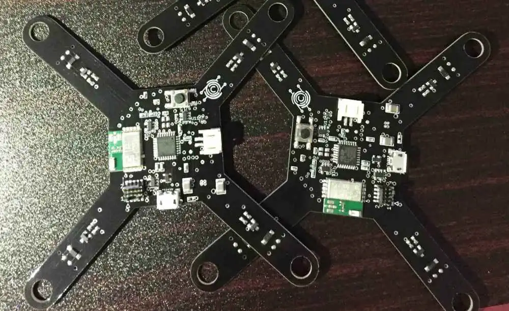
The contemporary drone PCB ecosystem encompasses far more than traditional circuit board design principles. Today’s advanced UAV systems integrate multiple subsystems including flight control units, sensor arrays, communication modules, power distribution networks, and payload interfaces, all of which must coexist harmoniously on a single board or interconnected multi-board system.

Flight control represents the most critical aspect of drone PCB design, as it directly impacts the vehicle’s ability to maintain stable flight, respond to pilot commands, and execute autonomous missions. The flight control unit typically incorporates high-performance microcontrollers or specialized flight processors that must process sensor data in real-time while maintaining precise control over motor speeds and servo positions.

Power distribution systems within drone PCBs face unique challenges due to the high current demands of brushless motors, the voltage sensitivity of onboard electronics, and the weight constraints inherent in aerial applications. Unlike terrestrial applications where weight is rarely a primary concern, every gram matters in drone design, making PCB weight optimization a crucial consideration.

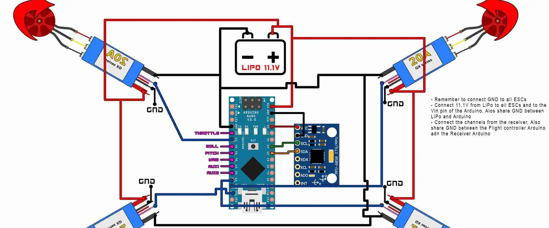
Flight Control System Architecture

The heart of any advanced drone PCB lies in its flight control system architecture, which must seamlessly integrate multiple sensor inputs, process complex algorithms, and provide real-time outputs to actuators and motors. Modern flight controllers typically employ 32-bit ARM Cortex processors running at frequencies exceeding 100MHz, providing the computational power necessary for advanced flight modes and autonomous operations.

Sensor integration represents one of the most challenging aspects of drone PCB design, as modern UAVs incorporate accelerometers, gyroscopes, magnetometers, barometric pressure sensors, GPS modules, and optical flow sensors. Each sensor type presents unique interface requirements, from high-speed SPI communications to precise analog signal conditioning. The drone PCB must provide clean, stable power to these sensitive components while minimizing electromagnetic interference that could compromise sensor accuracy.

Inertial measurement units (IMUs) require particular attention in drone PCB layout, as they form the foundation of flight stability. These sensors are extremely sensitive to vibration and electromagnetic interference, necessitating careful mechanical isolation and strategic placement away from high-current switching circuits. Advanced drone PCBs often incorporate multiple IMUs for redundancy, requiring sophisticated sensor fusion algorithms to combine multiple data streams into a single, reliable state estimate.

The real-time nature of flight control demands that the drone PCB architecture minimize latency between sensor input and actuator output. This requirement influences everything from processor selection to trace routing, as even microsecond delays can impact flight performance in high-speed or precision applications.

Power Distribution Network Design

Power distribution represents one of the most complex challenges in advanced drone PCB design, as the system must efficiently manage power flows ranging from high-current motor drives to sensitive low-voltage digital circuits. Modern drone power systems typically operate from lithium polymer batteries providing 11.1V to 25.2V, which must be converted to multiple voltage rails serving different subsystems.

The drone PCB power distribution network must handle several critical requirements simultaneously. Motor electronic speed controllers (ESCs) may draw currents exceeding 30 amperes during peak operation, while flight control processors require clean, stable 3.3V or 5V supplies with minimal ripple. Camera gimbals and sensors often require additional voltage rails, creating a complex web of power requirements that must be efficiently managed.

Switching power supplies have become the standard for drone PCB applications due to their superior efficiency compared to linear regulators. However, the high-frequency switching nature of these supplies introduces electromagnetic interference challenges that must be carefully managed through proper layout techniques and filtering strategies. The drone PCB designer must balance efficiency, size, weight, and electromagnetic compatibility to achieve optimal performance.

Current sensing and monitoring capabilities are increasingly important in advanced drone PCBs, providing real-time feedback on system health and enabling sophisticated battery management features. These monitoring systems allow flight controllers to make intelligent decisions about power allocation, provide early warnings of impending system failures, and optimize flight parameters for maximum endurance.

Electromagnetic Compatibility Challenges

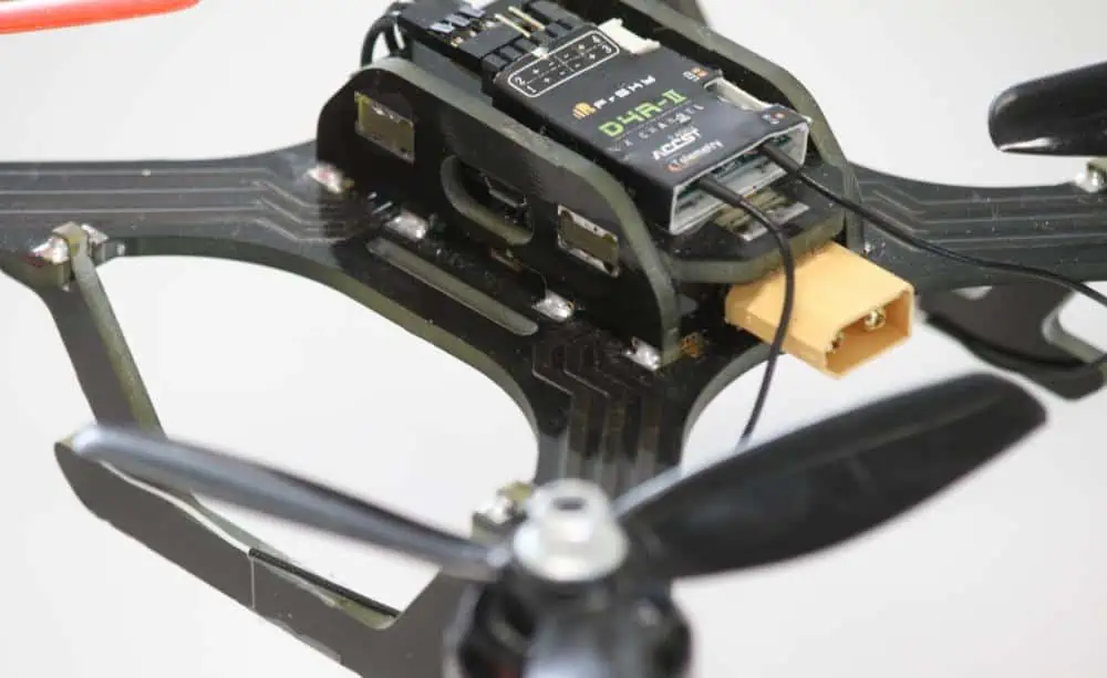
The confined space and high component density typical of drone PCBs create significant electromagnetic compatibility challenges that can compromise system performance if not properly addressed. Radio frequency interference from switching power supplies, high-speed digital circuits, and wireless communication modules can interfere with sensitive sensors, GPS reception, and radio control links.

Advanced drone PCB designs employ multiple strategies to minimize electromagnetic interference, including strategic component placement, proper grounding techniques, and the use of shielding structures. High-current motor drive circuits are typically isolated from sensitive analog circuits, while communication modules are positioned to minimize interference with other subsystems.

Ground plane design plays a crucial role in drone PCB electromagnetic compatibility, as improper grounding can create ground loops that introduce noise and interference. Advanced designs often employ multiple ground planes or split ground techniques to isolate different circuit blocks while maintaining proper return paths for high-frequency signals.

The increasing use of wireless communication systems in drones, including WiFi, Bluetooth, and proprietary radio links, adds another layer of complexity to electromagnetic compatibility design. These systems must coexist with other onboard electronics without causing mutual interference, requiring careful frequency planning and antenna placement.

Thermal Management Strategies

Thermal management represents a critical yet often overlooked aspect of drone PCB design, as the confined spaces and limited airflow typical of UAV applications can lead to component overheating and performance degradation. Power-hungry components such as processors, power regulators, and motor drivers generate significant heat that must be effectively dissipated to maintain reliable operation.

The drone PCB thermal design must account for both steady-state and transient thermal conditions, as component temperatures can vary dramatically during different flight phases. High-power maneuvers may cause temporary spikes in component temperatures that must be managed without compromising system reliability.

Advanced thermal management techniques for drone PCBs include the use of thermal vias to conduct heat through the board substrate, copper pour areas to spread heat across larger surface areas, and strategic component placement to avoid thermal hotspots. In some cases, active cooling solutions such as small fans or heat pipes may be incorporated, though these add weight and complexity.

The selection of appropriate PCB materials becomes crucial in high-temperature applications, as standard FR-4 substrates may not provide adequate thermal performance for demanding applications. Advanced materials such as metal-core PCBs or ceramic substrates may be required for the most challenging thermal environments.

Component Selection and Integration

The selection and integration of components for advanced drone PCBs requires careful consideration of multiple factors including performance, reliability, size, weight, and cost. Every component choice impacts overall system performance, making the selection process critical to mission success.

Microcontroller selection forms the foundation of drone PCB design, with factors including computational performance, peripheral availability, real-time capabilities, and power consumption all playing important roles. Modern flight controllers often employ dual-core processors or heterogeneous processing architectures that combine high-performance application processors with dedicated real-time control units.

Sensor selection requires balancing performance requirements with size and power constraints. High-performance inertial measurement units provide superior accuracy and stability but may consume more power and occupy more board space than lower-performance alternatives. The drone PCB designer must carefully evaluate these trade-offs based on specific mission requirements.

Power management components represent another critical selection area, as the efficiency and reliability of voltage regulators directly impact flight time and system reliability. Advanced power management integrated circuits provide sophisticated features such as power sequencing, fault protection, and telemetry capabilities that enhance overall system performance.

Manufacturing and Quality Considerations

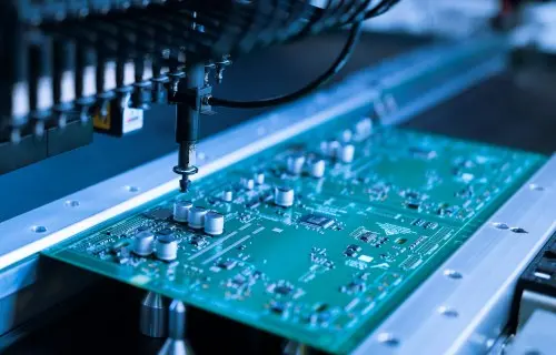
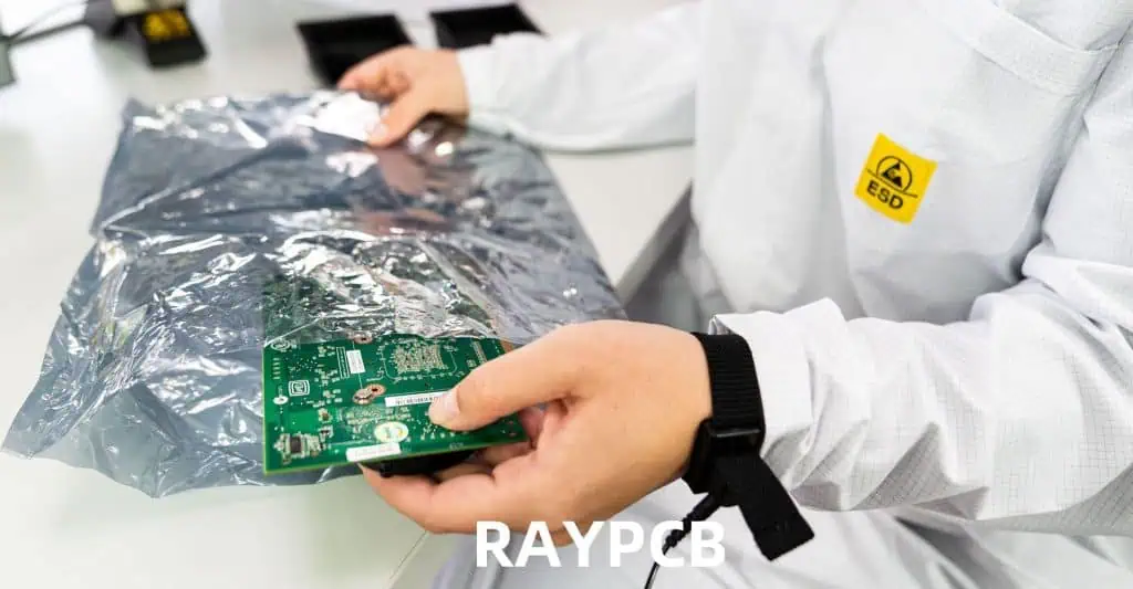
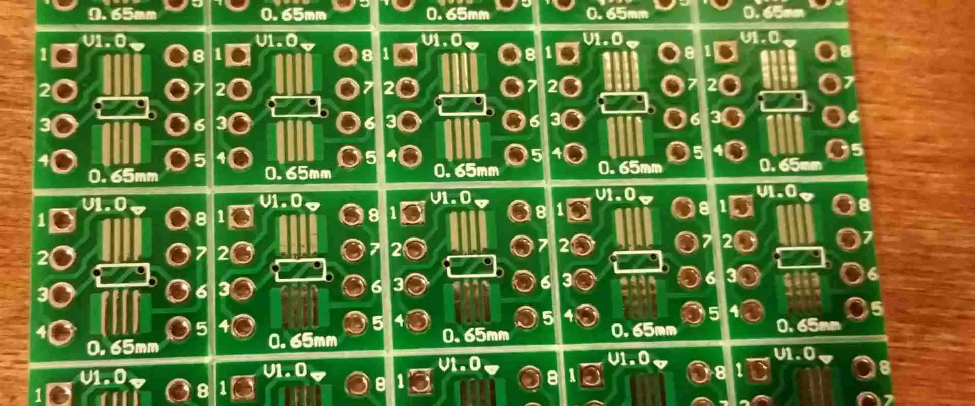
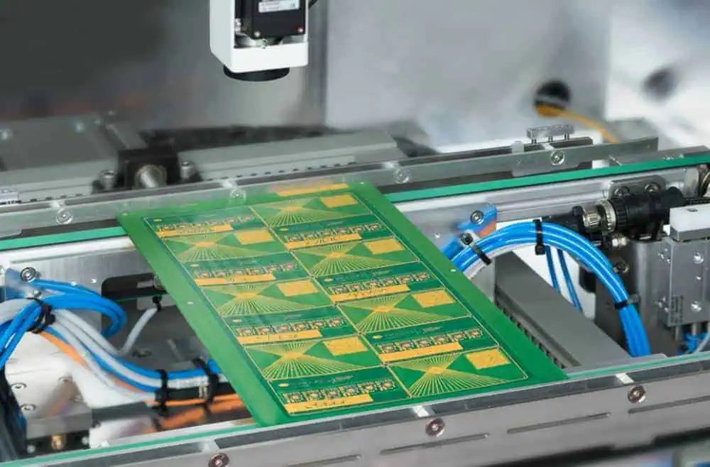
The manufacturing of advanced drone PCBs requires specialized processes and quality control measures to ensure reliable operation in demanding environments. The high component density and mixed-signal nature of drone circuits place stringent requirements on manufacturing tolerances and assembly processes.

Surface mount technology (SMT) assembly has become the standard for drone PCB manufacturing due to its superior density and reliability compared to through-hole techniques. However, the small component sizes and tight spacing typical of drone applications require advanced assembly equipment and careful process control to achieve acceptable yields.

Quality control measures for drone PCBs must address both electrical performance and mechanical reliability, as the vibration and shock environments encountered in flight can cause component failures or solder joint fatigue. Specialized testing procedures including vibration testing, thermal cycling, and accelerated aging may be required to validate design reliability.

The use of automated test equipment (ATE) becomes increasingly important as drone PCBs become more complex, providing comprehensive functional testing that would be impractical to perform manually. These test systems can verify not only basic electrical functionality but also dynamic performance characteristics such as sensor response times and control loop stability.

Future Trends and Innovations

The future of drone PCB design is being shaped by several emerging trends and technologies that promise to further enhance UAV capabilities while addressing current limitations. Advanced materials, new component technologies, and innovative design approaches are driving the next generation of drone electronics.

Three-dimensional PCB structures represent an emerging trend that promises to further increase component density while reducing overall system size and weight. These advanced structures allow components to be mounted on multiple layers of the PCB, creating truly three-dimensional electronic systems that maximize space utilization.

The integration of artificial intelligence and machine learning capabilities directly into drone PCBs is becoming increasingly practical as specialized AI processors become smaller and more power-efficient. These capabilities enable advanced autonomous behaviors and adaptive control algorithms that can improve flight performance and mission success rates.

Advanced power management technologies, including wireless power transfer and energy harvesting capabilities, are being explored as methods to extend flight endurance and reduce dependence on traditional battery systems. These technologies may fundamentally change how drone power systems are designed and integrated.

Conclusion

Advanced drone PCB design represents a complex engineering challenge that requires expertise across multiple disciplines and careful consideration of numerous competing requirements. The successful integration of flight control systems, power distribution networks, sensor arrays, and communication modules requires a holistic approach that considers not only individual component performance but also system-level interactions and emergent behaviors.

As drone technology continues to evolve and UAVs take on increasingly sophisticated missions, the demands placed on drone PCB designs will only increase. Future designs must balance performance, reliability, size, weight, and cost while incorporating new technologies and capabilities that enable next-generation autonomous flight systems.

The key to successful drone PCB design lies in understanding the unique requirements and constraints of aerial applications while applying advanced engineering principles and best practices. By carefully considering factors such as electromagnetic compatibility, thermal management, power distribution, and manufacturing requirements, designers can create drone PCBs that enable reliable, high-performance UAV operations across a wide range of applications and environments.

Success in this field requires continuous learning and adaptation as new technologies emerge and mission requirements evolve. The most effective drone PCB designs will be those that not only meet current requirements but also provide the flexibility and scalability necessary to accommodate future enhancements and capabilities.

Everything You Should Know About 2.5K Resistor

2.5K Resistor

A 2.5k resistor is an electronic component that has a resistance value of 2.5 kilo-ohms. Additionally, it is equivalent to 2500 ohms. Moreover, Resistors are passive components that are also present in electronic circuits to control the flow of electric current. Furthermore, A resistor’s resistance value is in ohms. In fact, it determines the amount of current that will flow through it when on a given voltage.

The 2.5k resistor is a relatively common resistance value in a variety of electronic circuits. In fact, it typically assists in controlling the flow of current or to limit the voltage in a circuit. Furthermore, the resistance value of a 2.5k resistor is high enough to provide significant resistance to current flow. However, it is not so high that it becomes impractical for use in most circuits.

2.5k resistors are available in a variety of different packages, including through-hole and surface-mount packages. Additionally, engineers make them from a variety of different materials, such as carbon, metal film, or wire-wound resistors. In fact, each of these materials has different properties that make it suitable for different types of applications.

Top 6 Manufacturers of 2.5K Resistors in China

Here are six of the top manufacturers of 2.5k resistors in China:

ยท Yageo Corporation

Firstly, Yageo is a leading global manufacturer of electronic components, including resistors. The company offers a wide range of resistors, including 2.5k resistors.

ยท Walsin Technology Corporation

Walsin is a major manufacturer of electronic components, including resistors. The company produces a wide range of resistors, including 2.5k resistors, in different configurations. In contrast to other companies, they are reputable in their durability and quality.

ยท Ralec Electronic Corporation

Ralec is a leading manufacturer of passive components, including resistors. The company produces a range of resistors, including 2.5k resistors, in various sizes and packaging options.

ยท UniOhm Technology Inc.

UniOhm is a leading manufacturer of resistors, including 2.5k resistors, and other passive components. The company offers a wide range of resistors in different sizes and configurations.

ยท Shenzhen Topmay Electronic Co. Ltd.

Topmay is a major manufacturer of electronic components, including resistors.

ยท Suzhou Rihua Precision Technology Co. Ltd.

Rihua is a leading manufacturer of resistors and other electronic components. The company also produces a range of resistors, including 2.5k resistors, in various sizes and configurations.

Uses of 2.5K Resistors

FULL PCB MANUFACTURING Quote

One of the most common uses of 2.5k resistors is in voltage divider circuits. Specifically, a voltage divider circuit is helpful in splitting a voltage into smaller fractions for measurement or other purposes. To create a voltage divider, engineers connect two 2.5k resistors in series. This splits the input voltage into two equal parts. Voltage dividers assist in a wide range of electronic circuits, including sensor circuits, power supplies, and audio circuits.

In transistor circuits, 2.5k resistors are often used to bias the base of the transistor. This is necessary to set the operating point of the transistor and ensure that it operates within its linear region. By selecting the proper resistance value, the biasing voltage can be set to the desired level.

In digital circuits, 2.5k resistors commonly work as pull-up and pull-down resistors. These resistors are here to ensure that a signal line is in a known state when no other devices are driving it. Pull-up resistors are used to hold a signal line high. On the other hand, pull-down resistors are helpful to hold a signal line low. Pull-up and pull-down resistors work a lot in microcontroller circuits and communication circuits.

To control the flow of electric current in electronic circuits, resistors work as passive components. A 2.5k resistor, which has a resistance value of 2.5 kilo-ohms, is equivalent to 2500 ohms and is a common resistor value in many circuits. Additionally, a resistor’s resistance value is in ohms and determines the current flow through it on a given voltage.

One application of a 2.5k resistor is as a current-limiting resistor in LED circuits, which are sensitive to overcurrent and can burn out if the current is too high. By selecting the right resistance value, engineers limit the current flowing through the LED to a safe level. As a result, current-limiting resistors are essential to ensure the longevity and reliability of LEDs.

In oscillator timing circuits, a 2.5k resistor can work as part of the timing network to generate periodic waveforms such as a sine wave or square wave. By combining a 2.5k resistor with a capacitor, a timer circuit can be created that generates a square wave output. As engineers adjust the frequency of the output by changing the resistance or capacitance values, oscillator circuits become integral to a variety of applications, including clock circuits, radio circuits, and digital signal processing.

In amplifier circuits, 2.5k resistors work to bias the amplifier, which sets the operating point and ensures that it functions within its linear region. With proper bias voltage setting, amplifiers can produce better performance and lower distortion. Amplifiers serve a lot in a wide range of electronic circuits, including audio amplifiers, power amplifiers, and instrumentation amplifiers.

Final Note

2.5k resistors are a commonly used electronic component that are present in a variety of applications. These resistors serve a lot to limit current, bias transistors, and amplifiers, and as pull-up and pull-down resistors in digital circuits. They can also work as part of oscillator timing circuits and in voltage divider circuits.

The resistance value of 2.5k is a relatively common value that is readily available from a range of electronic component suppliers. This makes it a convenient choice for circuit designers who need a specific resistance value.

Overall, 2.5k resistors are a versatile component that are useful in a wide range of electronic circuits. They are an essential component in LED circuits to ensure that the LED is not out of order by excessive current. They are helpful in voltage divider circuits to split an input voltage into smaller fractions. Also, it is good in transistor and amplifier circuits to set the biasing voltage. Their versatility and availability make them a valuable component in many electronic circuit designs.

Why use PCB Plated Slots for Best Practices?

PCB Slot

Printed circuit boards remain at the heart of most electronic appliances, and their manufacture involves several steps. A crucial component of PCB design is the PCB slot, and manufacturers must have a thorough understanding of it before starting the production of any device.

The benefits of incorporating grooves in a printed circuit board are numerous and should not be underestimated. There are various types of PCB slots, making it essential to have an in-depth understanding of these slots.

What are PCB Plated Slots?

A slot in a PCB is a larger opening that cannot be created through conventional drilling techniques. It must be cut out using a routing tool during the production of the printed circuit board. These slots can either be plated or unplated, depending on the manufacturer’s specifications.

Types of PCB Plated Slots

The two primary types of printed circuit board grooves are plated & unplated.

ยท Plated slot

In the production of circuit boards, the plated slot has a layer of copper coating. This slot type does not have a circular shape and features copper on both the top and bottom surfaces, making it best for electrical linkages. The Plated through-hole slots are suitable for component encapsulation and are a common feature in multi-layer circuit boards.

In the manufacture of circuit boards, various components are used for PCBs assembly. Most through-hole components have circular holes to accommodate either round or square leads. This configuration is prevalent in most through-hole assemblies. However, some components use rectangular leads that cannot fit into circular holes. In these cases, a plated slot is a more appropriate choice.

For large blade-style connectors, it is advisable to use plated through slots as the size of the pins increases. Smaller components can use round holes with rectangular pins, but these holes consume extra space. Plated grooves are more suitable for designs with limited space.

ยท Non plated slot

The unplated slot has a hole that is larger than the size of the copper pad, and in some cases, there may not be any copper. In an unplated slot, the copper of the pad overlaps. This sort of slot is produced by drilling once the electroless copper process has been completed.

Slots in the Printed Circuit Board profile

FULL PCB MANUFACTURING Quote

The most straightforward method of defining the slots is to display the slots/cut-outs and the PCB profile in a Gerber mechanical layer. If your PCB design software does not have a mechanical layer, an additional layer is required. If you are unsure which layer is the correct one, kindly indicate the slots in a README file.

To ensure safety, it is advisable to define the slots in the drill file using X and Y dimensions in specific CAD systems. Defining the slots in only the copper or legend layer is discouraged as it may result in misunderstandings or oversights on the part of PCB manufacturers. For optimal results, kindly inform our engineers or mark any slots or cut-outs on your PCB when placing an order.

What is the Smallest PCB Slot?

The minimum width for a groove on a rigid-flex & flex PCB is 0.50 millimeters, with a minimum length of 1.0 millimeters. It is due to the rigidness of rigid-flex and rigid PCBs, which requires the use of Mechanically controlled numerical control milling for creating the slots. On the other hand, flex circuits are thin, allowing them to be cut using a laser.

A longer slot length results in a straighter slot. Remember that the minimum length of a slot must be two times the width of the groove. For example, if the width of the groove is 0.6milimetre, the length of the slot should be 1.20mm.

Slots Milling

The manufacturer removes the grooves from the rigid printed circuit board material through milling. The process involves the use of a Non-computer Numeric Control grooving tool which operates similarly to a CNC machine. Note that the inside corners of the cutouts will have a rounded edge. It is crucial to consider this aspect in enclosure design.

The minimum radius for an inner corner is 0.5millimeterss, while the smallest device used in routing PCBs is 1.0 millimeters. The milling of slots creates air gaps for the voltage on the PCB.

Plated & Non-plated Slots in Printed Circuit Board design

The printed circuit board fabrication procedure involves etching the copper sheet, which is then placed onto a substrate and drilled with holes. Before plating, these slots are non-conductive. For PCBs with multiple copper layers, manufacturers utilize the electroless deposition process.

Designers should be aware that not all slots require plating. Designers must follow the guidelines provided by manufacturers to determine which slots will be plated. In some cases, designers may have certain expectations for their circuit boards, only to receive a final product that differs significantly, such as with mounting slots.

For example, if your design relies on a specific slot being plated and it is not, this can lead to problems. To avoid such issues, it is essential to distinguish between plated and non-plated slots. This way, you can ensure that your design is executed correctly and avoid surprises upon receiving the final circuit board.

How to consider a PCB Slot as plated?

A slot can only be considered plated if it meets specific criteria. If it does not, it is considered a non-plated slot. In a plated slot, the copper of the pad and the solder stop mask must overlap. The copper of the pad must also be more comprehensive than the slot by at least six miles.

How to consider a PCB slot as non-plated?

Sometimes, a PCB slot may be non-plated for either mechanical/electrical reasons. If a slot does not meet the criteria for a plated slot, it is considered non-plated. For example, a slot is considered non-plated if the hole is larger than the size of the copper pad or if the copper overlays & is larger than the hole, with a clearance of 6 mils between the copper & hole. These conditions signify that the slot meets the requirements for the non-plated slot.

Conclusion

The design of slots in a PCB is a crucial aspect of printed circuit board design. It’s essential to have a solid understanding of how slots operate in a PCB design. Both non-plated & plated slots serve their purpose. However, plated slots are commonly used in the printed circuit board industry.

A Step-By-Step Guide to SMT Step soldering

electronic assembly soldering

Knowing how to solder is a requirement if you wish to create high-quality electronics. This method is frequently used with a soldering iron and, when properly applied, can produce positive results. Nonetheless, the question of how to learn soldering still stands. In this post, I’ll introduce you to the SMT soldering procedure and give you a thorough, step-by-step tutorial on how to put together an electrical component.

What is SMT soldering?

SMT soldering is a hand-operated technique for joining electronic parts to a circuit board. SMT, which refers to “Surface Mount Technology,” denotes that the soldering is carried out using a specialized tool called a “solder reflow oven” rather than a soldering iron. The steps and materials used in the SMT soldering process are described below.

Use of SMT Step soldering

Whether employed in a work environment or as a pastime, SMT soldering has several advantages. SMT soldering is a great way for novices to learn how to solder because it may expand their knowledge of electronics and electricity.

SMT soldering’s cost-effectiveness and quick production rate are additional benefits in the workplace. While retaining product quality can considerably save manufacturing costs.

Parts of SMT Step soldering.

SMT-Through-Hole-Soldering

A circuit board & electronic parts are two essential items for SMT soldering.

Choose a silk-screened Printed Circuit Board with soldered holes whenever possible to provide the best outcomes when working with a circuit board (not tin). These circuit boards typically cost between $1 and $3 and may be purchased online or in nearby maker spaces.

Or, you can save money by sketching the layout onto the copper foil. A copper-clad board, which describes a thin sheet of copper with holes and traces added via acid etching or sandblasting, is an additional choice.

Purchasing the essential electronic components for SMT soldering is simple, and there are numerous possibilities online. For example, Rayming printed circuit board and Assembly provides SMT parts in various price ranges. As an alternative, various electronic components are now available on websites like eBay or Amazon. It is crucial to use caution when choosing electronic components because some may only be appropriate for prototyping and will not be utilized in production components. So, it is imperative to ensure that the components you select are consistent with your desired result.

Stuff you need for SMT Step soldering

Before you begin, you’ll need:

ยท A soldering station

A soldering station that consists of a warm air furnace to heat the solder, a soldering iron to heat the adhered junction, and a soldering tip to melt the solder is used today to manufacture electronics. Using a solder station effectively requires carefully controlling the temperature of each component and avoiding overheating. Either the heat mode or the temporal mode can be used to achieve this.

ยท Some solder

The primary material needed to carry out this operation is solder. It is a tin and lead alloy that frequently includes silver. Compared to other soldering materials, solder is reasonably priced and has a greater melting temperature than steel.

ยท A soldering iron

Using a heat gun, a hot air furnace, and a soldering tip to melt the solder, electronic components are joined in today’s electronics manufacturing process. The most critical part of using a soldering iron is to heat each component and avoid overheating carefully. Use either the temperature option or the time option to accomplish this.

ยท A piece of circuitry

Often made of several layers of metal, electronic circuit boards have solder-filled holes that link the various components. The circuit board’s dimensions and shape change based on what it is designed to do. Printed circuit boards can be utilized, but I’ll show you how to make a simple LED circuit board in detail.

ยท A circuit diagram

Electronic components can be used in various ways, each with its benefits, in various designs. To understand the wire connections and the accompanying solder joints, however, most PCs require a schematic. Often, the circuit diagram is displayed as numbers on a grid.

Make SMT Step soldering

FULL PCB MANUFACTURING Quote

1. Preparation

Set up your tools, such as your soldering iron, solder, etc., properly. To protect the solder from heat damage and oxidation when it melts, it must be kept in a container that can withstand various temperatures. Finally, decide on a quiet workspace, such as a basement or garage, to start the procedure.

2. Preparation of copper board

Choose a copper board that has the correct dimensions and form for your circuitry. An integrated circuit board should be used if you want to build something more complex instead of, say, a conventional breadboard, which is suitable for prototyping (also known as a “chip” board). Chipboards cost more than breadboards, but soldering electronics on them is frequently simpler because there are fewer wires to join. A chip LED is needed, for example, when soldering SMD LEDs. As it helps to stabilize junctions and make them waterproof, filler material is also used in this situation.

3. Mixing the solder paste

To avoid burns, turn off each of your soldering irons before mixing the solder paste. Keep in mind that the filler metal is hot as it exits the nozzle. Use the needle to remove some solder paste from a reusable gun and inject it into a thermal container.

To prevent burning your fingers, permanently remove the tip of an integrated circuit laser pistol with a screwdriver. The solder paste must then be melted in a microwave / small pot before being combined with the solder. It’s recommended to hold the soldering iron in one hand while combining it with the other to avoid burns. Once combined, heat the solder using a clean spoon/spatula to ensure your circuit is connected correctly.

4. Making SMT

Now is the time to begin soldering! Set the temperature on your heating element to between 40 and 45 degrees Celsius. Although solder commonly melts at 113ยฐC, heat several parts at once. Avoid putting the pieces too near to one another since they can melt together and make it hard to move the other parts.

Please choose one of the parts and warm it on the soldering iron’s tip for testing. If it has sufficiently formed, move on to the following elements. If not, try again until everything is correctly fused.

Use a heat gun and a bit of solder to connect the parts after assembly. Test your work after a second and look for any extra solder that might be connected to the iron. Put more soldering on the junction to eliminate any extra solder if there is any.

You may make your prototype by following this procedure without having to have specialized abilities, although it does take time and patience. Beginners should focus on one component at a time while checking for any problems. The solder paste application process from the gun upon a pad is the next stage in using SMT to build your product.

Conclusion

This project showed how a low-cost printed circuit board might be made utilizing standard components and straightforward soldering procedures. Also, you now know how to solder using an integrated circuit laser and a hot air soldering machine. You have also gained knowledge of the fundamental components of reflow soldering.

What is Silkscreen PCB? Things you need to know

hdi PCB Manufacturers

Do you have to incur additional costs for silkscreen when designing or ordering your PCBs? If so, it’s essential to understand what silkscreen is.

The silkscreen layer is created by the designer as a separate layer and integrated with the other coats of a printed circuit board. Whether or not the fabricator applies the silkscreen (screen print) to the printed circuit board depends on whether the designer has included this request in the particular instructions. On the silkscreen layer, the designer may include various pieces of information.

  •  All elements on the circuit board are assigned reference designators.
  • components Orientation 
  •  components Polarity
  •  components Outline
  •  Test Points
  •  PCB version number
  •  Printed circuit board serial number
  • Testing certifications
  •  Manufacturerโ€™s logo
  • Warm symbols

If a PCB contains only SMCs/surface mount elements, the designer can utilize a single silkscreen layer for the upper layer of the circuit board. However, if the printed circuit board has THCs or through-hole components, the designer can divide the silkscreen into two parts. The top layer of the board has essential information on it, while the bottom layer has labels that show where things should go and which way they should face. When the circuit board is made, a special kind of ink is used that won’t mess up the parts that need to be soldered. The person designing the hdi circuit board must carefully choose the correct ink for the labels, so it doesn’t mess up the soldering parts.

 Methods Of Applying Silkscreen PCB

To manually transfer the information onto the PCB, the fabricator employs the silkscreen details to create a transfer screen. Alternatively, they may adopt modern techniques to print the information directly onto the printed circuit board, eliminating the need for a transfer screen.

ยท Manual Printing 

Manually printing a design onto a circuit board using a particular screen can be helpful if the lines are at least 0.007 inches thick and the design is accurate within 0.005 inches. The fabricator uses a unique nylon fabric to make a stencil that matches the design. They stretch this stencil onto a frame and use ink to print the design onto the circuit board. Finally, they bake the board in an oven to make sure the ink stays on the board.

ยท Liquid Photo Imaging

When line widths are thinner, like four mils, hand-set printing becomes unsuitable, and fabricators turn to the LPI method. To implement this method, they begin by coating the printed circuit board with a light-sensitive epoxy layer. They then transfer the screen print image onto the epoxy & reveal it to ultraviolet light. After exposure, they remove the undeveloped portion of the epoxy, departing the silkscreen image on the printed circuit board. The board then undergoes curing to fix the image in place.

The LPI method, while providing greater precision than the Letterpress printing technique, demands more ink consumption and longer setup time.

ยท Direct Legend Printing 

Out of all available methods, this one stands as the most precise yet costly. It involves a computer, Computer-Aided Design software, an inkjet projector, & acrylic ink. The computer commands the visualizer to deposit ink onto the printed circuit board, following the silkscreen design, and then undergo ultraviolet curing.

Why Use Silkscreen PCB?

FULL PCB MANUFACTURING Quote

Using silkscreen printing on the printed circuit board offers numerous advantages. One example is with the silkscreen print:

  • The reference designators can aid assemblers in precisely placing components on PCB.
  • Assemblers can quickly determine the polarity and orientation of components through the silkscreen print.
  • During troubleshooting or measurements, PCB technicians can identify the testing nodes on the board.
  • By recognizing warning signs for high potential, technicians can set appropriate voltage & current levels.
  • When repairing the PCB, technicians can readily identify which components must be replaced.

How To Design A Silkscreen PCB?

For better PCB part designation, assembly & testing, it is essential to ensure that the Silk print meets specific design specifications, as recommended by Rush printed circuit board USA. These specifications include:

  • Fonts โ€” When it comes to silkscreen print on a printed circuit board, not all fonts are appropriate. To ensure that the printed text is legible & readable, the designer should seek guidance from their contract producer regarding which fonts are suitable for the process.
  • Color โ€” When the fabricator places the silkscreen onto the solder mask coat, the ink color for the silkscreen must provide a noticeable difference from the color of this solder mask. While white is the most suitable color for a green PCB mask layer, any color that creates a clear contrast and makes it easy to read the text or design is also acceptable.
  • Clearance and Dimension โ€” To ensure legibility & readability, it is crucial to maintain proper clearance & dimensions for the lines & letters on the silkscreen. The designer should seek guidance from their contract producer to meet these requirements. The ink from the silkscreen printing mustn’t infringe upon the solder pads under any circumstances.
  • PCB Design Guidelines and DFM โ€” Including the details in the printed circuit board design guideline and DFM is necessary to establish a uniform design for silkscreens across various PCBs.

Conclusion

Rush printed circuit board USA suggests that incorporating silk screen printing on a printed circuit board can significantly enhance its quality & reliability. The addition of silkscreen aid in both the assembly & testing processes while also considerably reducing the time required for troubleshooting. Despite the added expense of Incorporating a silkscreen print layer, the improved printed circuit board quality & reliability makes it a valuable investment.

Comprehensive Guide to IPC Standards for PCB Assembly: Ensuring Quality & Reliability in Electronics Manufacturing

through-hole assembly process

In the ever-evolving world of electronics manufacturing, maintaining consistent quality and reliability is paramount. At the heart of this pursuit lies a set of industry-wide standards known as IPC Standards for PCB Assembly. These standards, developed by the Association Connecting Electronics Industries (formerly known as the Institute for Printed Circuits), serve as the backbone for ensuring excellence in printed circuit board (PCB) design, manufacturing, and assembly processes.

This comprehensive guide will delve deep into the world of IPC Standards for PCB Assembly, exploring their significance, key components, and impact on the electronics manufacturing industry. Whether you’re a seasoned professional or new to the field, this article will provide valuable insights into the standards that shape the quality and reliability of electronic devices we use every day.

Powered By EmbedPress

Understanding IPC Standards for PCB Assembly

What Are IPC Standards?

IPC Standards are a set of guidelines and specifications developed by the IPC (Association Connecting Electronics Industries) to ensure consistency, quality, and reliability in the electronics manufacturing industry. These standards cover various aspects of PCB design, fabrication, and assembly, providing a common language and benchmarks for manufacturers, suppliers, and customers worldwide.

The Importance of IPC Standards in PCB Assembly

IPC Standards for PCB Assembly play a crucial role in maintaining quality and reliability in electronics manufacturing. Here are some key reasons why these standards are essential:

  1. Quality Assurance: By adhering to IPC Standards, manufacturers can ensure that their PCB assemblies meet industry-recognized quality benchmarks.
  2. Consistency: Standards provide a uniform approach to PCB assembly, reducing variations and inconsistencies across different manufacturers and production runs.
  3. Cost Reduction: Implementing standardized processes can lead to improved efficiency and reduced waste, ultimately lowering production costs.
  4. Customer Confidence: Products manufactured in compliance with IPC Standards instill greater confidence in customers, as they are assured of the quality and reliability of the end product.
  5. Global Compatibility: IPC Standards are recognized worldwide, facilitating international trade and collaboration in the electronics industry.

Read more about:

Key IPC Standards for PCB Assembly

IPC-A-610: Acceptability of Electronic Assemblies

IPC-A-610 is one of the most widely used standards in the electronics industry. It provides visual acceptance criteria for electronic assemblies and is often referred to as the “bible” of the industry.

Key Features of IPC-A-610:

  1. Three Classes of Products: The standard defines three classes of electronic products based on reliability requirements:
    • Class 1: General Electronic Products
    • Class 2: Dedicated Service Electronic Products
    • Class 3: High-Performance/Harsh Environment Electronic Products
  2. Visual Inspection Criteria: It provides detailed guidelines for visual inspection of various aspects of PCB assembly, including component placement, soldering, and overall board quality.
  3. Defect Classification: The standard classifies defects into three categories:
    • Accept: Meets the minimum requirements
    • Process Indicator: May require process improvement but is acceptable
    • Defect: Requires rework or repair
  4. Illustrated Examples: The standard includes numerous photographs and illustrations to help inspectors identify and classify defects accurately.

IPC-J-STD-001: Requirements for Soldered Electrical and Electronic Assemblies

IPC-J-STD-001 is a companion standard to IPC-A-610, focusing specifically on the materials and processes used in producing soldered electrical and electronic assemblies.

Key Aspects of IPC-J-STD-001:

  1. Material Requirements: It specifies the requirements for materials used in soldering, including solder alloys, fluxes, and cleaning agents.
  2. Process Control: The standard outlines procedures for controlling various aspects of the soldering process, such as temperature profiles and cleanliness.
  3. Acceptance Criteria: It provides detailed acceptance criteria for soldered connections, including through-hole and surface mount technology (SMT) assemblies.
  4. Specialized Requirements: The standard includes specific requirements for unique assembly types, such as wire and terminal connections.

IPC-7711/7721: Rework, Modification and Repair of Electronic Assemblies

This pair of standards provides guidelines for reworking, modifying, and repairing electronic assemblies. They are essential for maintaining the quality and reliability of PCBs throughout their lifecycle.

Key Features of IPC-7711/7721:

  1. Rework Procedures: The standards outline step-by-step procedures for various rework operations, such as component removal and replacement.
  2. Modification Guidelines: They provide guidance on how to modify existing PCB assemblies without compromising their integrity.
  3. Repair Techniques: The standards describe techniques for repairing damaged PCBs and components, ensuring that repaired assemblies meet the same quality standards as new ones.
  4. Tools and Equipment: They specify the appropriate tools and equipment to be used for rework, modification, and repair operations.

Implementing IPC Standards in PCB Assembly

Training and Certification

To effectively implement IPC Standards for PCB Assembly, it’s crucial to have a well-trained workforce. The IPC offers various training and certification programs to ensure that personnel involved in PCB assembly are knowledgeable about the standards and their application.

Key Training Programs:

  1. IPC-A-610 Certified IPC Specialist (CIS): This program trains individuals in the visual acceptance criteria for electronic assemblies.
  2. IPC J-STD-001 Certified IPC Specialist: This certification focuses on soldering processes and acceptance criteria.
  3. IPC-7711/7721 Certified IPC Specialist: This program trains technicians in rework, modification, and repair techniques for PCB assemblies.

Establishing Quality Control Processes

Implementing IPC Standards requires robust quality control processes throughout the PCB assembly workflow. Here are some key steps to establish effective quality control:

  1. Incoming Inspection: Implement thorough inspection procedures for incoming materials and components to ensure they meet IPC Standards before entering the assembly process.
  2. In-Process Quality Checks: Conduct regular quality checks at various stages of the assembly process to catch and correct issues early.
  3. Final Inspection: Perform comprehensive final inspections of assembled PCBs using IPC-A-610 criteria to ensure the final product meets all quality requirements.
  4. Documentation and Traceability: Maintain detailed records of all quality control activities, including inspection results, rework operations, and any deviations from standards.

Continuous Improvement

Adhering to IPC Standards for PCB Assembly is not a one-time effort but a continuous process of improvement. Here are some strategies for ongoing enhancement:

  1. Regular Audits: Conduct internal audits to assess compliance with IPC Standards and identify areas for improvement.
  2. Data Analysis: Analyze quality control data to identify trends and recurring issues, allowing for targeted process improvements.
  3. Staff Training: Provide ongoing training to keep staff up-to-date with the latest revisions to IPC Standards and best practices in PCB assembly.
  4. Supplier Management: Work closely with suppliers to ensure they adhere to IPC Standards, maintaining quality throughout the supply chain.

Advanced Topics in IPC Standards for PCB Assembly

IPC-6012: Qualification and Performance Specification for Rigid Printed Boards

While not directly related to assembly, IPC-6012 is crucial for ensuring the quality of the PCBs used in assembly processes. This standard sets the requirements for qualification and performance of rigid printed boards.

Key Aspects of IPC-6012:

  1. Performance Classes: Similar to IPC-A-610, it defines three classes of PCBs based on reliability requirements.
  2. Qualification Requirements: It outlines the tests and inspections required to qualify a PCB for use in electronic assemblies.
  3. Electrical Properties: The standard specifies requirements for electrical properties such as impedance control and dielectric withstanding voltage.
  4. Physical Properties: It defines requirements for physical properties like dimensional stability and thermal stress resistance.

IPC-2221 and IPC-2222: Generic Standard on Printed Board Design

These standards provide guidelines for PCB design, which directly impacts the assembly process. Understanding these standards can help assembly professionals work more effectively with design teams.

Key Features of IPC-2221 and IPC-2222:

  1. Design Considerations: They cover various aspects of PCB design, including layer stackup, conductor spacing, and pad design.
  2. Design for Manufacturability (DFM): The standards provide guidance on designing PCBs that are easier to manufacture and assemble.
  3. Thermal Management: They include guidelines for designing PCBs with effective thermal management, crucial for high-power applications.
  4. Signal Integrity: The standards address design considerations for maintaining signal integrity in high-speed circuits.

IPC-4101: Specification for Base Materials for Rigid and Multilayer Printed Boards

This standard is essential for understanding the properties of the base materials used in PCB manufacturing, which can impact assembly processes and final product reliability.

Key Aspects of IPC-4101:

  1. Material Classifications: It defines various types of base materials and their properties.
  2. Performance Requirements: The standard specifies performance requirements for different material types, including electrical, mechanical, and thermal properties.
  3. Testing Methods: It outlines standardized testing methods for evaluating base material properties.
  4. Environmental Considerations: The standard addresses environmental factors, such as flammability ratings and halogen content.

The Future of IPC Standards for PCB Assembly

High Volume Assembly Line

As technology continues to evolve, IPC Standards for PCB Assembly must adapt to new challenges and innovations in the electronics industry. Here are some trends and developments to watch:

Miniaturization and High-Density Interconnect (HDI)

As electronic devices become smaller and more complex, PCB assemblies are moving towards higher density and finer pitch components. IPC Standards will need to evolve to address the challenges associated with assembling and inspecting these highly miniaturized boards.

Flexible and Rigid-Flex PCBs

The increasing use of flexible and rigid-flex PCBs in various applications, from wearable devices to aerospace, will require updates to existing standards and potentially new standards specifically addressing these technologies.

Advanced Materials

The development of new PCB materials, such as those designed for high-frequency applications or extreme environments, will necessitate updates to standards related to material specifications and assembly processes.

Industry 4.0 and Smart Manufacturing

As the electronics manufacturing industry embraces Industry 4.0 concepts, IPC Standards may need to incorporate guidelines for integrating smart manufacturing technologies, such as real-time process monitoring and data analytics, into PCB assembly processes.

Sustainability and Environmental Considerations

With growing emphasis on sustainability, future revisions of IPC Standards may include more comprehensive guidelines for environmentally friendly manufacturing processes, material selection, and end-of-life considerations for electronic assemblies.

Conclusion: The Enduring Importance of IPC Standards for PCB Assembly

In conclusion, IPC Standards for PCB Assembly play a vital role in ensuring the quality, reliability, and consistency of electronic products in an increasingly complex and demanding industry. From providing clear acceptance criteria for assembled PCBs to guiding the entire manufacturing process, these standards serve as the foundation for excellence in electronics manufacturing.

As we’ve explored in this comprehensive guide, adhering to IPC Standards offers numerous benefits, including improved quality assurance, cost reduction, and enhanced customer confidence. By implementing these standards through proper training, robust quality control processes, and a commitment to continuous improvement, manufacturers can position themselves at the forefront of the electronics industry.

Looking to the future, IPC Standards will continue to evolve, addressing new technologies, materials, and manufacturing processes. Staying informed about these developments and actively participating in the standards development process will be crucial for companies wanting to maintain a competitive edge in the global electronics market.

Whether you’re a PCB assembly professional, a quality control specialist, or an electronics engineer, understanding and implementing IPC Standards is essential for success in today’s high-tech manufacturing landscape. By embracing these standards and the principles they represent, we can collectively drive innovation, quality, and reliability in the electronics that shape our world.

PCB Instant Quote For Manufactures And Suppliers

Instant PCB Quote

The opportunity to contribute to developing electronic devices with impedance control & PCB manufacture is unmatched in the modern era. There has never been a greater need for quick PCB assembly and prototyping services. Consumers increasingly want connectivity to a wide range of devices. They want to use their smartphones or tablets to control many parts of their lives, including the sprinkler system or thermostat.

In the battle to effectively and swiftly launch their products onto the market, many businesses confront fierce competition. The printed circuit board assembly service & electronics manufacturing industries have undergone significant change due to these demands.

Warnings for PCB instant quote

Companies have been manufacturing electronic gadgets with PCB for a long time. Large corporations with significant orders, long lead times, and no requirement for quick iterations had their needs met by traditional manufacturing infrastructure. Be aware of the following red flags if you want a PCB quote.

  • It is required to email specific files, including the printed circuit board design, Gerber file, bill of materials, and other pertinent information.
  • It typically takes several emails back and forth with an authorized sales representative to get a PCB quote, and it can take weeks or even days to complete.
  • Ascertain that you have all the required materials and pieces.
  • To keep someone updated on the status of your project, be sure you call or send an email.
  • Offshore locations could make communication and travel more difficult.
  • You run the risk of losing your possessions to underworld organizations.
  • The seller does not accept prototyping orders even if they were; the price would be prohibitively exorbitant.
  • The vendor does not offer inventory management or fulfillment services.
  • Production either has a significant minimum order requirement or has much higher costs for small / low-volume runs.

What is a PCB instant quote?

On-demand manufacture, sometimes referred to as cloud manufacturing, offers assistance for the creation of PCBs & impedance-controlled electrical devices from the initial design to the final delivery to the customer, in contrast to the conventional paradigm.

With our platform, designers can manage inventory and follow projects at any time through their browser and receive a fast PCB quote in just a few minutes, thanks to internet-based technologies.

By combining small batch runs, prototyping orders, and larger purchases, on-demand production enables distributors to aggregate numerous small orders.

This strategy also lowers expenses and makes it possible to do away with minimum order limitations that would usually be charged to the consumer.

Developers may concentrate on making the best product and marketing it in their market thanks to the approach to PCB assembly & device manufacturing.

You may get a PCB estimate quickly by uploading your designs to online portals. The manufacturing services provider will subsequently take action to realize your vision, and you will have continuous access to the status of your project without financial surprises.

Benefits of PCB instant quote

Customized rigid flex PCB

Everyone with a fresh product concept has more access to the advancement of PCB technology & device production. Entrepreneurs produce novel ideas, small businesses release specialized products, and even giant corporations permit their engineers to focus on personal projects in addition to oneโ€˜s research & development activities.

ยท Purchasing Teams

On-demand manufacturing can still be helpful to you even if you don’t have any engineering experience. Provide the required PCB file, for example, a Gerber file, to a trustworthy manufacturer like RayMing, and you’ll get a price for your printed circuit board assembly.

Businesses must discover a means to quickly launch high-quality products on the market if they want to succeed wildly. It is not an option to hold off on getting a PCB quote.

ยท Small Businesses

Start-ups and expanding companies often do not require multiple orders to secure competitive prices from major manufacturers. Also, they favor prompt deliveries and try to retain small stocks. By lowering the costs related to small numbers of runs, on-demand manufacturing satisfies the requirements of such companies.

Some PCB assembly companies also provide fulfillment and inventory management services and software to connect a company’s website with its manufacturing platform. Employees may concentrate on necessary business demands thanks to this integration’s cost-cutting benefits. For tiny startups and established companies, on-demand manufacturing is a dependable approach to spur growth.

ยท Engineers

Engineers can engage with RayMing to get a quick and transparent PCB estimate at every level of development and production for their PCB assembly needs, regardless of their position in research & development, printed circuit board design organizations, or small businesses.

With on-demand production, you are not constrained by conventional production methods and may produce prototypes more often and iterate.

Benefits Of Working With A Partner With PCB Instant QUOTE Services

ยท Reduces risk

Miscommunications may be avoided, risks can be minimized, and needless shipping expenses can be removed by working with a dependable partner throughout the production process. To guarantee a successful outcome, it’s crucial to assess the experience and dependability of your potential partners thoroughly.

ยท Market Faster

Rapid prototyping, prompt PCB quotations, and user-friendly online tools contribute to streamlining the procedure and enabling enterprises to introduce new goods or improvements to the market more quickly.

ยท Focus on the customers & product

Companies frequently outsource specific tasks to concentrate on their core capabilities and crucial tasks. They can organize their processes more effectively and increase efficiency by assigning specific duties to others.

Conclusion

We’ve reached the end of our discussion of the PCB Quote. Keep in mind to work with a business that offers the most affordable quote and excellent PCB fabrication services. Please get in touch with us if you’ve any more inquiries.

How to design step groove PCB in Altium designer?

V-Groove PCB

With advancements in technology and an ever-increasing demand for excellent performance, designs incorporating high-speed signals are becoming increasingly prevalent. Altium Designer 16 recognizes the growing necessity for robust support of high-speed design and introduces several significant enhancements for the definition & routing of high-frequency signals.

Altium Designer offers an extended Signal, known as an xSignal, that allows designers to define a signal path containing multiple nets & series components. High-speed design rules can be applied to target this signal. In the latest version of the software, the pin or package delay, which contributes to signal delay, is now factored into the overall length of the xSignal. Additionally, the intelligent xSignals wizard has been updated to include heuristics for creating xSignals by the DDR3 or DDR4 specification, with plans to support other interface kinds in the future. Further improvements have been made to differential pair skew adjustment, enabling more rapid and precise length matching between and within pairs.

Solving the Design Challenges

laser-cut-pcb

These challenges can be met with Altium’s PCB design technologies.

ยท Create Boards of any Shape or groove PCB.

Altium Designer provides flexibility in board design, allowing for boards of various shapes and types, such as rigid, rigid-flex / pure flex. A rigid-flex design can accommodate many layer stack-ups, with the option to create additional coverlays. Components integrated on the internal routing layer, maximizing the use of space. 

With support for up to thirty-two signal layers and sixteen plane layers, the board can be customized to meet specific requirements. To make things more flexible, you can divide plane layers into as many parts as you want. You can also create smaller areas within those divided parts if you need to.

Altium Designer offers 32 mechanical construction layers that can be repurposed for specialized manufacturing layers, such as defining glue dots.

 Additionally, the board’s shape can be created externally and loaded into the printed circuit board editor using file formats such as DWG, DXF, or STEP. It allows for precise customization of the board shape, enabling designers to meet specific project requirements.

ยท A Flexible Workspace with groove PCB and Polar Grids

The designer has the flexibility to choose between metric/imperial units and work with either cartesian/polar grids. Additionally, it is possible to overlay many snap grids, which can be limited to objects or components only. The board size can vary significantly, ranging from minuscule to as large as 100×100 inches. Furthermore, design objects can be created as small as 0.001mil.

In addition to the grid alignment system, there is a helpful hotspot snap feature that can override the snap-to-grid and attract the cursor to the hotspot of an object when it’s within a user-defined range. This tool makes it easier to work with objects that aren’t lined up perfectly, like connecting wires to the pins of a part that’s measured in inches on a board that’s measured in millimeters.

In addition, the program allows you to customize where objects will snap, and it also provides guides to help you align objects in a specific direction. All of these features are valuable tools for achieving precise object placement.

How to Make groove PCB in Altium penalization?

FULL PCB MANUFACTURING Quote

As the electronics industry continues to evolve, many products within this sector have established complex upstream & downstream support enterprises. This industrial chain is naturally formed in a specific environment, which includes mature product design, manufacturing, design, packaging, assembly testing, and wholesale channels. As a result, the link between design & manufacturing is crucial, and the two are interdependent.

The processing of PCB boards is a crucial component of electronic product development and manufacturing, from design completion to production. Most of the plain circuit boards that PCBs work on are put together using machines that place electronic components on them.

As electronic products evolve towards smaller and lighter designs, a new problem arises. PCB manufacturing is well-suited for creating small boards, but when it comes to prototype PCB assembly, placement machines become a challenge. It is especially true for electronic components just some centimeters square in size, as the small area makes it challenging to assemble the product on the placement machine. It can create significant issues, particularly in the manufacturing line.

To address this issue, it becomes necessary to create a small printed circuit board that can be assembled in an area that meets the assembler’s needs or utilize a panelization method easier for SMT assembly, such as using a yin & yang board. Typically, manufacturing board factories offer panelization services. Still, by utilizing the Electronic design automation (EDA) software in the design process, designers can more clearly convey their intentions and reap several benefits, including:

  1. Enables creation in the desired orientation.
  2. The panelized layout is linked to the source circuit board, and any changes made to the source board are automatically reflected in the panelized circuit board.
  3. Allows for the combination of multiple different boards.
  4. Supports the use of yin & yang boards. 

How to put different Circuit Boards together?

Rotation Panelization

To combine different PCBs, select a printed circuit board file and arrange it in an array. Then, choose another printed circuit board file and arrange it similarly.

It is important to note that when combining different PCBs, the no. of layers & thickness settings of each PCB must be identical to ensure successful processing.

To make a yin & yang board, utilize the panel function to arrange a set of boards, then arrange another set of boards in the same way. Once this is done, choose the mirror function. It is important to note that the yin & yang boards should have identical layer thicknesses to be successfully combined and processed.

In addition to Altium Panelize, we can also provide a guide for penalizing PCBs using EasyEDA, Eagle, and KiCad software. If interested, we can allocate time to create a detailed guide for each program.

What is V Groove PCB?

V-groove printed circuit boards result from the splitting process of PCBs, which involves cutting the boards and leaving some material to hold them together. In the final stages of production, the V-groove printed circuit boards are profiled and separated from the production panel, either by routing / V-cut scoring. When manufacturing V-groove printed circuit boards, specific rules must be followed to ensure proper production.

Rules for manufacturing groove PCB

  •        Make sure that the board has a spacing of 0mm.
  • Keep the spacing between the outline & V-scoring line at 0.35mm.
  • The V-scoring line must be straight and either horizontal or vertical.
  • The V-groove printed circuit boards should have a minimum size of 75 x 75 mm and a size of 450 x 1245 mm.

Panelization Methods

Various methods exist for penalizing breakaway tab printed circuit boards, each with advantages and disadvantages. The design of the board and the panel itself typically play a significant role in determining the most suitable method for panelization. It is essential to consider these factors when deciding which approach to use.

  • Components: The placement of components on a PCB is just as critical as the choice of components themselves, particularly for sensitive connectors & components that can significantly impact the optimal panelization & breakout method.
  • Design: When determining the optimal panelization method, the board’s layout is the most crucial factor. The clearance between the edge of the board and its components may render some methods less suitable than others.
  • Materials: The materials used in mouse-bites printed circuit boards can affect the choice of the best panelization method. Certain materials are prone to splintering during the procedure of breakaway, which limits the suitable methods. The Breadth of the circuit board is also a critical factor. Thin boards are more likely to break during assembly, while thick boards may pose challenges during the breakaway process.

Why Your PCB Needs Fiducial Marks: Placement & Design Tips

In the modern printed circuit board (PCB) manufacturing, precision is paramount. Every component must be placed with utmost accuracy to ensure the final product functions as intended. This is where fiducial marks come into play. These small but crucial elements are the unsung heroes of PCB assembly, guiding automated machines to place components with pinpoint accuracy. In this comprehensive guide, we’ll explore the ins and outs of fiducial marks, their importance in PCB manufacturing, and how to implement them effectively in your designs.

What is a Fiducial Mark?

Fiducial marks, often simply called fiducials, are small, precisely placed features on a PCB that serve as reference points for automated assembly equipment. These marks are typically circular or cross-shaped and are made of bare copper with a protective coating to prevent oxidation.

Key Characteristics of Fiducial Marks:

  • Usually circular or cross-shaped
  • Made of bare copper
  • Coated to prevent oxidation
  • Precisely placed on the PCB
  • Act as reference points for assembly machines

Fiducial marks are essential in ensuring that components are placed accurately on the PCB during the assembly process. They provide a consistent reference point that assembly machines can use to orient themselves and make necessary adjustments.

Read more about:

How Does a Fiducial Mark Help in Manufacturing?

Fiducial marks play a crucial role in the PCB manufacturing process, particularly during the automated assembly stage. Here’s how they contribute to the production of high-quality PCBs:

1. Machine Orientation

Automated pick-and-place machines use fiducial marks to orient themselves relative to the PCB. This ensures that the machine knows exactly where it is on the board at all times.

2. Compensation for Misalignment

Even slight misalignments in board positioning can lead to significant errors in component placement. Fiducial marks allow machines to detect and compensate for these misalignments.

3. Improved Accuracy

By providing precise reference points, fiducial marks enable assembly machines to place components with high accuracy, often within fractions of a millimeter.

4. Consistency Across Boards

Fiducial marks ensure consistency in component placement across multiple boards in a production run, leading to more reliable and uniform products.

5. Error Reduction

The use of fiducial marks significantly reduces the likelihood of errors in component placement, thereby minimizing defects and improving overall product quality.

How Do I Add Fiducials to My Boards?

PCB Fiducial Mark

Adding fiducial marks to your PCB design is a crucial step in ensuring accurate assembly. Here’s a step-by-step guide to help you incorporate fiducials into your boards:

  1. Determine the Number of Fiducials: Decide how many fiducial marks you need based on your board’s size and complexity. Most designs require at least three fiducials.
  2. Choose Strategic Locations: Place fiducials in corners or along edges where they won’t interfere with components or traces.
  3. Use Your PCB Design Software: Most PCB design software packages have built-in tools for adding fiducial marks. Look for options like “Add Fiducial” or “Place Fiducial Marker.”
  4. Set the Correct Size: Typically, fiducial marks should be 1mm to 3mm in diameter. Consult with your PCB manufacturer for their specific requirements.
  5. Ensure Proper Clearance: Leave ample clearance around each fiducial mark to ensure it’s easily recognizable by assembly machines.
  6. Verify Placement: Double-check that your fiducials are placed correctly and don’t interfere with other elements on the board.
  7. Include in Manufacturing Files: Make sure your fiducial marks are included in the Gerber files you send to your PCB manufacturer.

Remember, the exact process may vary depending on your PCB design software, but these general steps should guide you in adding fiducials to your boards effectively.

Types of Fiducial Marks

Fiducial marks come in various types, each serving specific purposes in PCB assembly. Understanding these types can help you choose the most appropriate fiducials for your design. Let’s explore the different types of fiducial marks:

1. Panel Fiducial Markers

Panel fiducial markers are used when multiple PCBs are manufactured on a single panel. These fiducials are placed on the panel itself, outside the boundaries of individual boards.

Key Features:

  • Located on the panel, not on individual PCBs
  • Used for initial alignment of the entire panel
  • Typically larger than board-level fiducials

2. Global Fiducial Markers

Global fiducial markers are placed on individual PCBs and serve as primary reference points for the entire board.

Key Features:

  • Usually placed in opposite corners of the PCB
  • Used for overall board alignment
  • Essential for accurate component placement across the entire board

3. Local Fiducial Indicators

Local fiducial indicators are used for precise alignment of specific components or areas on the PCB.

Key Features:

  • Placed near critical or high-precision components
  • Provide additional reference points for localized accuracy
  • Particularly useful for fine-pitch or BGA components

4. Round or Dot Fiducial Marks

Round or dot fiducial marks are the most common type, featuring a simple circular shape.

Key Features:

  • Easy to create and recognize
  • Typically 1mm to 3mm in diameter
  • Provide a clear, unambiguous reference point

5. Crosshair Fiducial Marks

Crosshair fiducial marks feature intersecting lines forming a cross or plus sign.

Key Features:

  • Offer precise centering capabilities
  • Useful for high-precision applications
  • Can be more challenging to manufacture than round fiducials

6. Copper Fiducial Marks

Copper fiducial marks are created using the copper layer of the PCB.

Key Features:

  • Typically covered with a solder mask to prevent oxidation
  • Provide good contrast for optical recognition
  • Cost-effective and easy to implement

7. Grid Pattern Fiducial Marks

Grid pattern fiducial marks consist of multiple fiducials arranged in a grid layout.

Key Features:

  • Useful for large or complex boards
  • Provide multiple reference points across the board
  • Enable more precise alignment and component placement

8. Corner Fiducial Marks

Corner fiducial marks are specifically placed at the corners of the PCB.

Key Features:

  • Typically used in sets of three (three corners)
  • Provide reference points for overall board orientation
  • Essential for initial alignment in the assembly process

By understanding these different types of fiducial marks, you can make informed decisions about which ones to use in your PCB design, ensuring optimal alignment and component placement accuracy during the assembly process.

Advantages of Using Fiducial Marks for PCB Assembly

Incorporating fiducial marks into your PCB design offers numerous benefits that contribute to improved manufacturing efficiency and product quality. Let’s explore the key advantages:

1. Enhanced Accuracy in Component Placement

Fiducial marks provide precise reference points for automated assembly equipment, resulting in highly accurate component placement. This accuracy is crucial for:

2. Increased Production Efficiency

By enabling automated equipment to quickly and accurately align boards, fiducial marks help to:

  • Reduce setup time
  • Increase throughput
  • Minimize production delays

3. Improved Quality Control

Fiducial marks contribute to better quality control by:

  • Ensuring consistent component placement across all boards
  • Reducing the likelihood of misaligned components
  • Facilitating easier visual inspection

4. Cost Reduction

While adding fiducial marks might seem like an extra step, they actually help reduce costs by:

  • Minimizing rework and repairs
  • Reducing scrap rates
  • Improving overall yield

5. Compatibility with Advanced Manufacturing Techniques

Fiducial marks support advanced manufacturing processes, including:

  • High-speed automated assembly
  • Flip-chip technology
  • Micro-BGA placement

6. Flexibility in Design

Fiducial marks offer design flexibility by:

  • Allowing for more complex board layouts
  • Supporting a wider range of component types and sizes
  • Enabling tighter component spacing

7. Enhanced Reliability

The precision offered by fiducial marks leads to enhanced product reliability through:

  • Reduced risk of short circuits from misaligned components
  • Improved solder joint quality
  • Consistent performance across all manufactured boards

8. Simplified Troubleshooting

In case of assembly issues, fiducial marks can:

  • Help identify misalignment problems quickly
  • Facilitate easier board-level repairs
  • Aid in root cause analysis of manufacturing defects

By leveraging these advantages, PCB designers and manufacturers can produce higher quality boards more efficiently, leading to improved product performance and customer satisfaction.

Fiducial Mark Design Guidelines

Designing effective fiducial marks is crucial for ensuring their functionality in the PCB assembly process. Here are some key guidelines to follow when incorporating fiducial marks into your PCB design:

1. Shape

The shape of your fiducial marks plays a significant role in their effectiveness:

  • Recommended: Circular shapes are most commonly used and easily recognized by assembly equipment.
  • Alternative: Square or diamond shapes can also be effective but may require specific machine settings.
  • Avoid: Complex or irregular shapes that may be difficult for machines to interpret.

2. Size

The size of fiducial marks is critical for accurate recognition:

  • Diameter: Typically between 1mm and 3mm.
  • Consistency: Maintain uniform size across all fiducials on the board.
  • Machine Compatibility: Consult with your assembly house for their specific size requirements.

3. Material

The material used for fiducial marks affects their visibility and durability:

  • Copper: Most commonly used due to its conductivity and contrast with the board surface.
  • Coating: Apply a protective coating (e.g., ENIG) to prevent oxidation.
  • Avoid: Using solder mask as the sole material for fiducials, as it may not provide sufficient contrast.

4. Clearance

Proper clearance around fiducial marks ensures they are easily recognizable:

  • Solder Mask Clearance: Maintain a solder mask clearance of at least 0.5mm around the fiducial.
  • Component Clearance: Keep a minimum distance of 5mm between fiducials and nearby components or board edges.
  • Copper Pour Clearance: Ensure no copper pour or traces within 2mm of the fiducial mark.

Additional Design Considerations

  1. Quantity: Include at least three fiducial marks per board for optimal alignment.
  2. Placement:
    • Position fiducials in at least two opposite corners of the board.
    • For larger boards, consider adding additional fiducials along the edges.
  3. Symmetry: Avoid symmetrical placement that could lead to 180-degree rotation errors.
  4. Visibility: Ensure fiducials are visible and not obscured by components or other board features.
  5. Consistency: Use the same design for all fiducial marks on a given board.
  6. Documentation: Clearly document fiducial marks in your design files and manufacturing specifications.
  7. Verification: Double-check fiducial mark placement and specifications before finalizing your design.

By adhering to these design guidelines, you can ensure that your fiducial marks effectively serve their purpose in guiding automated assembly equipment, leading to more accurate and efficient PCB production.

Conclusion

Fiducial marks are indispensable elements in modern PCB design and manufacturing. Their role in ensuring precise component placement, improving production efficiency, and enhancing overall product quality cannot be overstated. By understanding the different types of fiducial marks, their advantages, and following best practices in their design and implementation, PCB designers can significantly improve the manufacturability and reliability of their boards.

Remember, while fiducial marks may seem like small details, they have a big impact on the success of your PCB production. Always consult with your PCB manufacturer to ensure your fiducial mark design aligns with their equipment capabilities and requirements. With proper implementation of fiducial marks, you’re setting the stage for efficient, high-quality PCB assembly that meets the demanding standards of today’s electronics industry.

Whether you’re working on a simple two-layer board or a complex multi-layer design, incorporating well-designed fiducial marks is a step towards manufacturing excellence. So, the next time you’re laying out a PCB, give fiducial marks the attention they deserve โ€“ your assembly team and end-users will thank you for it.

What is a DIP Switch PCB in Electronics?

DIP Switch PCB

DIP literally means โ€œDual In-Line Package.โ€ It is an electronic term used for types of a switch. DIP switch is a group of small-size manual switches for electronics. They are specially designed to be grouped with other printed circuit boards. The term DIP either refers to a single switch, a unit of multi-switch, or the complete unit. 

DIP switches are essentially used to modify a device’s operating mode by allowing users to manage the electric current that flows around a PCB, electronic accessory, and expansion card. 

DIP switches provide the user with the ability to tailor the behavior of the electronic equipment in question when mounted on a PCB along with other components, enabling complete leverage over the specific task the device will conduct in a variety of applications and defined scenarios. DIP switches are commonly displayed as a series of small toggle (on/off) switches installed consecutively on a piece of high-temperature thermoplastic polymer, much like a number of miniature traditional light switches.

A group of DIP switches nearly always requires considerable dexterity from the user to toggle every switch between the state of on and off because they are often quite small as a whole component. In actual use, this function is frequently carried out with the tip of a pointed pencil or another appropriately shaped tool because individual switches are typically too small to be operated with a finger.

DIP switches are often widely used, reasonably priced components that make it easy to choose and switch between different hardware or device configurations. DIP switches have the drawback of requiring the user to physically open the device in order to access the PCB and then manually activate the switches from there. However, they are typically far less expensive than alternatives like programmable chips or programming control panels.

This article gives you a detailed insight into the types, forms, and functions of a group of DIP switches and the various types and varieties of devices and applications available in the market.ย 

Uses of DIP Switch PCB

pin switch

Due to the downscaling trend and the decreasing costs of other equivalent solutions, DIP switches are less popular than they previously were. Nonetheless, they continue to be utilized in a variety of test circuits and industrial applications. 

This is due to the fact that physical DIP switches provide a very affordable choice for system control that is also incredibly simple to connect to an existing Printed circuit board or prototype circuit model. DIP switches can significantly decrease the need for extra hardware to conduct a wider range of output jobs by providing a quick and handy way to physically observe the settings that are currently chosen without turning the system on first.

Application of DIP Switch PCB

In modern circuits and devices, the most widely used applications of DIP switches include the following.

The setting up of numerous possibilities for Computer hardware and accessories. This comprises expansion modules, motherboards, hard drives, video cards, modems, as well as other add-ons or auxiliary parts. There are still many garage doorway systems that use DIP switches.

They’re frequently used in universal remote controllers to stop electrical interference from causing accidental device control. For each pair of receivers and transmitters in this scenario, a distinct radio frequency will be configured using the DIP switch.

How does DIP Switch PCB Work?

FULL PCB MANUFACTURING Quote

Conventional surface-mounted DIP switches are offered as an arrangement of straightforward two-terminal (1/0 or on/off) mechanical switches that have been constructed inside a thermoplastic polymer block container. Although technically, they are just an alternative to the traditional jumper; they are frequently referred to as “jumpers” despite the fact that their general purpose is extremely similar.

The “dual in-line” part of the acronym relates to how the contact pins on the underside of the DIP switch block, which connect to the PCB or prototype directly, are arranged. They are placed in two parallel lines, hence the name “dual in-line.” In general, a given module will have twice quite so many contact wires as switches.

When choosing a certain device function and needing to toggle many switches to get the desired output mode, DIP switches come in handy. Among the most frequent uses for a DIP switch is on the motherboard of a computer, where different configuration options can be accessible by flipping various switches.

A typical DIP switch could include one, two, four, seven, eight, ten, sixteen, or more toggle, slide, rocker, and rotatory slide installed on one tiny block. Although DIP switches are simple parts, their value lies in the fact that by placing numerous toggles in parallel, each one can be individually switched to the 1/0 position, potentially opening up a vast array of possible combinations to explore.

With a typical DIP switch matrix, every single toggle is disconnected from the others. A flexible suspension underneath the switch reacts to the motion of the rocker or slider and bends gently up or down in order to shut or open a passive contact below when a switch on such a DIP switch is shifted between its on and off settings. Correspond with a wide range of potential device outputs/functions.

As per their safe operational power, improved power quality, and voltage, DIP switches are generally divided into groups for various functions and applications. Users must follow and adhere to the manufacturer’s guidelines while using a specific DIP switch in order to avoid issues like a self-welded switch and electric curving while switching that could result in performance instabilities or device breakage.

Benefits of DIP Switch PCB

The following are just a few of the numerous advantages of DIP switch matrices in specific circuits, design procedures, and types of devices:

  1. For certain higher-end Dual In-line Package switch versions, gold contacts are frequently a choice, providing significantly improved durability and efficiency.
  2. They serve as a practical upgrade to more worn-out jumpers.
  3. Units range from 1 to 32 poles, providing a wide range of utility and versatility.
  4. In busy production operations, longer poles upon certain designs help save loading times.
  5. In order to place DIP switches on a Printed Circuit Board or prototype, their poles can easily be adjusted by being chopped to the appropriate level.

Conclusion

Although there has been a slight decline in the use of DIP switches in some contemporary applications due to the rising cost-effectiveness of application control panels as well as computer-controlled onboard chips, DIP switches still are viewed as a very appealing option in a variety of design workflows, device testing, and industrial settings.