Temperature Rise Estimations in Rogers High Frequency Circuit Boards Carrying Direct or RF Current (PDF Download)

Rogers RO4360

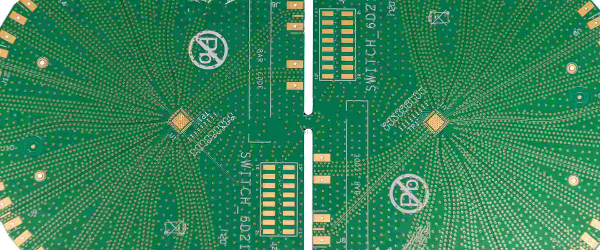
In the realm of high-frequency electronics, Rogers Corporation’s circuit board materials have become a go-to choice for engineers and designers. These materials offer excellent electrical and thermal properties, making them ideal for applications ranging from telecommunications to aerospace. However, as frequencies increase and power densities rise, thermal management becomes a critical concern. This article delves into the methods and considerations for estimating temperature rise in Rogers high-frequency circuit boards when carrying direct or RF current.

Understanding Rogers High Frequency Materials

Before diving into temperature rise estimations, it’s crucial to understand the characteristics of Rogers’ high-frequency materials.

Key Properties of Rogers Materials

Rogers Corporation offers several product lines designed for high-frequency applications, including:

  1. RO4000ยฎ Series
  2. RT/duroidยฎ
  3. CLTE-XTโ„ข
  4. AD Series

These materials are known for their:

Thermal Conductivity

Thermal conductivity is a key factor in heat dissipation. Rogers materials typically have thermal conductivity values ranging from 0.3 to 1.5 W/mยทK, depending on the specific product. This property significantly influences how heat is distributed across the board.

Powered By EmbedPress

Factors Affecting Temperature Rise

Several factors contribute to temperature rise in high-frequency circuit boards:

  1. Current density
  2. Frequency of operation
  3. Trace geometry
  4. Substrate thickness
  5. Copper thickness
  6. Ambient temperature
  7. Presence of thermal vias or heat sinks

Current Density and Its Impact

Current density, measured in amperes per square meter (A/mยฒ), is a primary driver of temperature rise. As current density increases, so does the heat generated in the conductor due to resistive losses.

Frequency Considerations

At high frequencies, additional phenomena come into play:

  • Skin effect: Current tends to flow near the surface of conductors, effectively reducing the cross-sectional area and increasing resistance.
  • Dielectric losses: The substrate material absorbs some energy, converting it to heat.

Methods for Estimating Temperature Rise

Rogers ULTRALAM 3850

Several approaches can be used to estimate temperature rise in Rogers circuit boards:

  1. Analytical calculations
  2. IPC-2152 standard
  3. Finite Element Analysis (FEA)
  4. Empirical testing

Analytical Calculations

For simple cases, particularly with DC current, analytical methods can provide a good starting point. The basic equation for temperature rise (ฮ”T) due to power dissipation is:

ฮ”T = (P * ฮธ) / A

Where:

  • P is the power dissipated (W)
  • ฮธ is the thermal resistance (ยฐCยทmยฒ/W)
  • A is the area of heat dissipation (mยฒ)

For a PCB trace, we can estimate the power dissipation using:

P = Iยฒ * R

Where:

  • I is the current (A)
  • R is the resistance of the trace (ฮฉ)

The resistance R can be calculated based on the trace dimensions and the resistivity of copper.

IPC-2152 Standard

The IPC-2152 standard, “Standard for Determining Current-Carrying Capacity in Printed Board Design,” provides charts and equations for estimating temperature rise based on current, trace width, and copper thickness. While not specifically designed for high-frequency applications, it can serve as a useful reference point.

Finite Element Analysis (FEA)

FEA software allows for more complex and accurate simulations, taking into account:

  • 3D geometry of the board and components
  • Material properties of all elements
  • Heat sources (including RF losses)
  • Cooling mechanisms (conduction, convection, radiation)

Popular FEA tools for PCB thermal analysis include ANSYS, COMSOL Multiphysics, and Siemens Simcenter.

Empirical Testing

While simulation and calculations are valuable, empirical testing remains crucial, especially for high-frequency applications. Methods include:

Read more about:

Estimating Temperature Rise for DC Current

For DC current, the process is relatively straightforward:

  1. Calculate the resistance of the trace based on its dimensions and copper resistivity.
  2. Determine the power dissipation using P = Iยฒ * R.
  3. Estimate the area of heat dissipation, considering both the trace surface and the surrounding board area.
  4. Use the thermal resistance of the Rogers material to calculate the temperature rise.

Example Calculation:

Let’s consider a 50 mm long, 1 mm wide trace on RO4350B material with 1 oz copper thickness, carrying 2A DC.

  1. Trace resistance: R โ‰ˆ 8.9 mฮฉ (calculated based on trace dimensions)
  2. Power dissipation: P = 2ยฒ * 0.0089 = 0.0356 W
  3. Dissipation area: A โ‰ˆ 100 mmยฒ (assuming some spread beyond the trace)
  4. Thermal resistance: ฮธ โ‰ˆ 0.5 ยฐCยทinยฒ/W (from Rogers datasheet, converted to metric)
  5. Temperature rise: ฮ”T = (0.0356 * 0.5) / (100 * 10^-6) โ‰ˆ 178ยฐC

This simplified calculation suggests a significant temperature rise, highlighting the importance of proper thermal management even for DC applications.

Estimating Temperature Rise for RF Current

Estimating temperature rise for RF current is more complex due to additional factors:

  • Skin effect
  • Dielectric losses
  • Radiation losses

Skin Effect Considerations

At high frequencies, current flows primarily near the surface of the conductor, effectively increasing its resistance. The skin depth (ฮด) can be calculated as:

ฮด = โˆš(ฯ / (ฯ€ * f * ฮผ))

Where:

  • ฯ is the resistivity of copper
  • f is the frequency
  • ฮผ is the magnetic permeability

For frequencies above 1 GHz, the skin depth in copper is less than 2 ฮผm, significantly increasing the effective resistance.

Dielectric Losses

The loss tangent (tan ฮด) of the Rogers material determines the dielectric losses. These losses contribute to overall heating and can be significant at high frequencies.

The power loss in the dielectric (Pd) can be estimated as:

Pd = 2ฯ€ * f * C * Vยฒ * tan ฮด

Where:

  • f is the frequency
  • C is the capacitance of the structure
  • V is the voltage
  • tan ฮด is the loss tangent of the material

Radiation Losses

At high frequencies, some power is lost through radiation. While this doesn’t directly contribute to board heating, it reduces the overall efficiency and can indirectly affect thermal performance.

Practical Approach to RF Temperature Rise Estimation

For RF applications, a combination of methods is often most effective:

  1. Use analytical methods to get a baseline estimate.
  2. Employ specialized RF simulation software (e.g., Ansys HFSS, CST Microwave Studio) to model EM fields and losses.
  3. Use thermal simulation software to convert RF losses into temperature distributions.
  4. Validate results through empirical testing.

Thermal Management Strategies

Once temperature rise has been estimated, various strategies can be employed to manage thermal issues:

  1. Increase copper weight: Thicker copper reduces resistance and improves heat spreading.
  2. Widen traces: Increases the cross-sectional area, reducing current density.
  3. Use thermal vias: Helps conduct heat to other layers or a ground plane.
  4. Implement heat sinks: Increases the surface area for heat dissipation.
  5. Forced air cooling: Improves convection cooling.
  6. Use of thermally conductive materials: Fills air gaps and improves heat transfer.

Case Study: High-Power RF Amplifier Board

Consider a high-power RF amplifier operating at 2.4 GHz on a Rogers RO4350B substrate. The amplifier outputs 50W of RF power, with an efficiency of 60%.

Approach:

  1. Calculate total power dissipation: 50W * (1/0.6 – 1) = 33.3W
  2. Use EM simulation to determine current distribution and losses in traces.
  3. Apply thermal simulation to estimate temperature distribution.
  4. Validate through infrared thermography.

Results might show hotspots near the amplifier output, requiring strategies like:

  • Increasing copper thickness on output traces
  • Adding thermal vias under the amplifier
  • Implementing a heat sink on the amplifier and critical trace areas

Conclusion

Estimating temperature rise in Rogers high-frequency circuit boards carrying direct or RF current is a complex but crucial aspect of high-frequency design. While analytical methods provide a starting point, the complexity of high-frequency effects often necessitates advanced simulation techniques and empirical validation.

Key takeaways:

  1. Consider both conductive and dielectric losses, especially at high frequencies.
  2. Use a combination of analytical, simulation, and empirical methods for accurate estimations.
  3. Implement appropriate thermal management strategies based on your estimations.
  4. Always validate your designs through testing, especially for critical high-frequency applications.

As frequencies and power levels continue to increase, thorough thermal analysis and management will remain essential for ensuring the reliability and performance of high-frequency circuits built on Rogers materials.

Device Attachment Methods and Wirebonding Notes for RT/duroid and RO4000 Series High Frequency Laminates (PDF Download)

Rogers RO4700 PCB

1. Introduction

RT/duroid and RO4000 series high-frequency laminates, produced by Rogers Corporation, are widely used in advanced RF and microwave applications. Proper device attachment and wirebonding techniques are crucial for ensuring optimal performance and reliability in circuits using these materials. This comprehensive guide explores various device attachment methods and provides detailed wirebonding notes specific to RT/duroid and RO4000 series laminates.

2. Overview of RT/duroid and RO4000 Series Laminates

2.1 RT/duroid Laminates

RT/duroid laminates are PTFE-based composites designed for high-frequency, low-loss applications. Key features include:

Common RT/duroid variants:

2.2 RO4000 Series Laminates

RO4000 series laminates are hydrocarbon ceramic-based materials offering a balance between performance and processability. Key features include:

  • Dk values ranging from 3.38 to 3.55
  • Low loss tangent
  • Stable electrical properties over frequency
  • FR-4-like processing capabilities

Common RO4000 variants:

Powered By EmbedPress

3. Device Attachment Methods

3.1 Soldering

Soldering is a common method for attaching devices to RT/duroid and RO4000 series laminates. However, special considerations are necessary due to the materials’ unique properties.

3.1.1 Solder Selection

  • Use high-temperature solders (e.g., Au80/Sn20, Au88/Ge12) for RT/duroid laminates to withstand subsequent assembly steps.
  • For RO4000 series, standard Sn63/Pb37 or lead-free alternatives like SAC305 can be used.

3.1.2 Surface Preparation

  • Ensure the laminate surface is clean and free from oxidation.
  • For RT/duroid, plasma cleaning or chemical etching may be necessary to improve adhesion.
  • RO4000 series typically requires standard FR-4 preparation techniques.

3.1.3 Temperature Control

  • For RT/duroid, use a temperature-controlled soldering iron set below the material’s maximum operating temperature (typically 280ยฐC).
  • RO4000 series can withstand standard soldering temperatures up to 280ยฐC for short durations.

3.1.4 Flux Selection

  • Use no-clean or easily removable fluxes to prevent residue-related issues.
  • For RT/duroid, choose fluxes compatible with PTFE surfaces.

3.2 Epoxy Attachment

Epoxy attachment is often preferred for sensitive devices or when precise positioning is required.

3.2.1 Epoxy Selection

  • For RT/duroid, use PTFE-compatible epoxies with good thermal and electrical properties.
  • For RO4000 series, standard conductive or non-conductive epoxies suitable for FR-4 can be used.

3.2.2 Application Techniques

  • Use automated dispensing equipment for precise epoxy placement.
  • Control epoxy thickness to ensure consistent electrical and thermal performance.
  • Consider using stencils for repeatable epoxy deposition.

3.2.3 Curing Process

  • Follow the epoxy manufacturer’s recommended curing profile.
  • For RT/duroid, ensure the curing temperature doesn’t exceed the material’s maximum operating temperature.
  • RO4000 series can typically withstand standard epoxy curing temperatures.

3.3 Eutectic Die Attach

Eutectic die attach is often used for high-reliability applications and provides excellent thermal and electrical conductivity.

3.3.1 Material Selection

  • Gold-tin (Au80/Sn20) and gold-germanium (Au88/Ge12) are common eutectic alloys used with RT/duroid and RO4000 series laminates.

3.3.2 Surface Metallization

  • Ensure proper metallization of both the die and the laminate surface.
  • For RT/duroid, specialized metallization techniques may be required to achieve good adhesion to the PTFE surface.

3.3.3 Process Control

  • Use precise temperature control to achieve proper eutectic bonding.
  • Implement inert atmosphere or forming gas to prevent oxidation during the bonding process.

Read more about:

4. Wirebonding Notes

Rogers RO4835 PCB

Wirebonding is a critical process for connecting devices to the circuit traces on RT/duroid and RO4000 series laminates. Proper techniques are essential for achieving reliable connections.

4.1 Surface Preparation for Wirebonding

4.1.1 RT/duroid Laminates

  • PTFE surfaces require special treatment to achieve good bondability.
  • Plasma etching with oxygen or CF4/O2 mixture can improve surface energy.
  • Chemical treatment using sodium naphthalene solution can also enhance bondability.

4.1.2 RO4000 Series Laminates

  • Standard cleaning procedures used for FR-4 materials are typically sufficient.
  • Plasma cleaning can be used to remove organic contaminants and improve bond strength.

4.2 Metallization Considerations

4.2.1 RT/duroid Laminates

  • Direct bonding to copper may be challenging due to the soft PTFE substrate.
  • Recommend using additional metallization layers:
    • Nickel (1-5 ยตm) as a barrier layer
    • Gold (0.5-1 ยตm) as a bondable surface

4.2.2 RO4000 Series Laminates

  • Standard metallization schemes used for FR-4 are generally suitable.
  • Typical stack-up: Copper > Nickel (2-5 ยตm) > Gold (0.05-0.1 ยตm)

4.3 Wirebonding Parameters

4.3.1 Gold Wire Bonding

  • Wire diameter: Typically 18-33 ยตm (0.7-1.3 mil)
  • Bonding force: 15-30 gf for RT/duroid, 20-40 gf for RO4000 series
  • Ultrasonic power: Adjust based on substrate hardness (lower for RT/duroid)
  • Bond time: 10-20 ms

4.3.2 Aluminum Wire Bonding

  • Wire diameter: Typically 25-33 ยตm (1-1.3 mil)
  • Bonding force: 20-40 gf for RT/duroid, 30-50 gf for RO4000 series
  • Ultrasonic power: Higher than gold wire, adjust based on substrate
  • Bond time: 15-30 ms

4.4 Temperature Considerations

  • For RT/duroid, maintain substrate temperature below 200ยฐC during bonding.
  • RO4000 series can typically withstand temperatures up to 280ยฐC for short durations.

4.5 Loop Profile Optimization

  • Optimize loop height and shape to minimize wire length and inductance.
  • Consider the coefficient of thermal expansion (CTE) mismatch between wire and substrate when designing loop profiles.

4.6 Bond Pad Design

  • Minimum pad size: 3-4 times the wire diameter
  • Recommended pad thickness: 3-5 ยตm for gold, 5-10 ยตm for aluminum
  • Include fiducials for automated bonding systems

5. Reliability Considerations

5.1 Environmental Factors

  • Both RT/duroid and RO4000 series laminates offer good resistance to humidity and chemicals.
  • For high-reliability applications, consider hermetic packaging to protect wirebonds and devices.

5.2 Thermal Management

  • RT/duroid laminates with high thermal conductivity (e.g., RT/duroid 6010.2LM) can aid in heat dissipation.
  • For RO4000 series, consider additional thermal management strategies for high-power applications.

5.3 Stress Mitigation

  • Use stress-relief loops in wirebonds to accommodate CTE mismatches.
  • Consider underfill materials for large devices to distribute stress.

5.4 Testing and Qualification

  • Perform pull and shear tests to verify bond strength.
  • Conduct environmental stress tests (temperature cycling, humidity, etc.) to ensure long-term reliability.

6. Advanced Techniques

6.1 Ribbon Bonding

  • Useful for high-current applications or where lower inductance is required.
  • Typically easier to implement on RO4000 series due to its higher rigidity compared to RT/duroid.

6.2 Automated Bonding

  • Both RT/duroid and RO4000 series are compatible with automated bonding equipment.
  • Proper fixturing and temperature control are critical, especially for RT/duroid laminates.

6.3 Flip-Chip Bonding

  • Can be used with both laminate series for reduced parasitics and improved thermal performance.
  • Requires careful consideration of underfill materials, particularly for RT/duroid laminates.

7. Troubleshooting Common Issues

7.1 Poor Bond Adhesion

  • For RT/duroid: Verify surface treatment effectiveness, consider alternative metallization.
  • For RO4000 series: Check for surface contamination, adjust bonding parameters.

7.2 Wire Breakage

  • Examine loop profile for stress concentrations.
  • Verify wire quality and bonding parameters.

7.3 Pad Lifting

  • Check metallization adhesion to the laminate.
  • Adjust bonding force and ultrasonic power.

7.4 Inconsistent Bond Quality

  • Ensure consistent surface preparation across the substrate.
  • Verify equipment calibration and maintenance.

Conclusion

Successful device attachment and wirebonding on RT/duroid and RO4000 series high-frequency laminates require a thorough understanding of the materials’ properties and careful process control. By following the guidelines outlined in this document and considering the unique characteristics of each laminate series, engineers and technicians can achieve reliable and high-performance RF and microwave assemblies.

It’s important to note that specific applications may require further optimization of these general guidelines. Always consult with Rogers Corporation’s technical support and conduct thorough testing for your particular use case to ensure optimal results.

Quick Reference Processing Guidelines RO4000 LoPro Laminates (PDF Download)

The Rogers RO4000 LoPro series of laminates are high-performance materials designed for advanced RF and microwave applications. These guidelines provide a quick reference for PCB fabricators and designers working with RO4000 LoPro laminates, ensuring optimal performance and reliability in the finished product.

1. Material Handling and Storage

1.1 Environmental Conditions

  • Store RO4000 LoPro laminates in a clean, dry environment.
  • Maintain temperature between 20ยฐC to 25ยฐC (68ยฐF to 77ยฐF).
  • Keep relative humidity between 40% to 60%.

1.2 Handling Precautions

  • Handle laminates with clean, lint-free gloves to prevent contamination.
  • Avoid bending or folding the material to prevent damage to the copper foil.
  • Use appropriate support when moving large panels to prevent flexing.

1.3 Acclimatization

  • Allow laminates to acclimatize to room temperature for 24 hours before processing.
  • This step helps prevent dimensional changes during subsequent processes.

Powered By EmbedPress

2. Inner Layer Preparation

2.1 Scaling and Artwork

  • Compensate for thermal expansion and contraction in the artwork.
  • Use the CTE (Coefficient of Thermal Expansion) values provided in the RO4000 LoPro data sheet.

2.2 Laminate Cutting

  • Use sharp, clean cutting tools to minimize stress and delamination.
  • Ensure cutting surfaces are smooth and burr-free.

2.3 Drilling

  • Use high-quality, sharp drill bits designed for FR4 materials.
  • Recommended drill speeds: 150 to 300 surface meters per minute.
  • Recommended chip loads: 0.05 to 0.10 mm/revolution for mechanical drilling.

2.4 Hole Wall Preparation

  • Desmear using plasma or chemical processes.
  • Optimize desmear time to avoid excessive removal of resin.

3. Copper Plating

3.1 Electroless Copper Deposition

  • Use standard FR4 processes for electroless copper deposition.
  • Ensure proper adhesion by optimizing the pre-treatment steps.

3.2 Electrolytic Copper Plating

  • Follow standard plating procedures used for FR4 materials.
  • Maintain uniform current distribution for even copper thickness.

4. Outer Layer Imaging and Etching

4.1 Photoresist Application

  • Ensure the laminate surface is clean and dry before applying photoresist.
  • Use standard dry film or liquid photoresists compatible with FR4 processes.

4.2 Exposure and Development

  • Optimize exposure times based on the resist manufacturer’s recommendations.
  • Develop using standard alkaline developers.

4.3 Etching

  • Use standard etchants such as ammoniacal or cupric chloride.
  • Monitor and control etch rates to prevent undercut.

Read more about:

5. Multilayer Lamination

5.1 Prepreg Selection

  • Choose appropriate Rogers prepreg materials compatible with RO4000 LoPro laminates.
  • Consider the final thickness and electrical requirements of the PCB.

5.2 Layup

  • Ensure all layers are clean and free from debris.
  • Use proper registration techniques to align layers accurately.

5.3 Lamination Parameters

  • Recommended lamination temperature: 182ยฐC to 199ยฐC (360ยฐF to 390ยฐF).
  • Recommended lamination pressure: 200-350 PSI (14-24 kg/cmยฒ).
  • Heating rate: 3ยฐC to 5ยฐC per minute (5.4ยฐF to 9ยฐF per minute).
  • Cool down rate: 3ยฐC to 5ยฐC per minute (5.4ยฐF to 9ยฐF per minute).

6. Final Fabrication Steps

6.1 Routing and Scoring

  • Use sharp, clean router bits to minimize burrs and stress.
  • Recommended router speed: 200 to 300 surface meters per minute.
  • Feed rate: 1.5 to 3 meters per minute.

6.2 Final Cleaning

  • Use alkaline or neutral cleaners compatible with RO4000 LoPro materials.
  • Avoid prolonged exposure to strongly alkaline solutions.

6.3 Solder Mask Application

  • Use standard solder masks compatible with high-frequency materials.
  • Follow the solder mask manufacturer’s recommended curing profile.

7. Surface Finish

7.1 HASL (Hot Air Solder Leveling)

  • Use lead-free HASL process if required.
  • Control temperature and exposure time to prevent excessive heat stress.

7.2 ENIG (Electroless Nickel Immersion Gold)

  • Follow standard ENIG processes used for FR4 materials.
  • Ensure proper thickness control for optimal RF performance.

7.3 Immersion Tin and Immersion Silver

  • These finishes are compatible with RO4000 LoPro laminates.
  • Follow standard process parameters for FR4 materials.

8. Special Considerations for High-Frequency Applications

8.1 Impedance Control

  • Use appropriate stackup design tools that account for the RO4000 LoPro material properties.
  • Consider frequency-dependent dielectric constant in calculations.

8.2 Signal Integrity

  • Maintain consistent copper thickness and line widths for critical traces.
  • Use proper grounding and shielding techniques to minimize EMI.

8.3 Thermal Management

9. Quality Control and Testing

9.1 Dimensional Stability

  • Verify final dimensions against design specifications.
  • Account for potential shrinkage or expansion during processing.

9.2 Electrical Testing

  • Perform standard electrical tests (continuity, isolation) as per IPC standards.
  • For high-frequency boards, consider additional RF performance testing.

9.3 Microsection Analysis

  • Conduct periodic microsection analysis to verify internal structure.
  • Check for proper resin fill, copper plating thickness, and layer alignment.

10. Troubleshooting Common Issues

10.1 Delamination

  • Possible causes: Inadequate lamination pressure, contamination, or improper handling.
  • Solution: Review lamination parameters and material handling procedures.

10.2 Poor Copper Adhesion

  • Possible causes: Insufficient surface preparation or improper etching.
  • Solution: Optimize desmear process and review copper treatment steps.

10.3 Inconsistent Impedance

  • Possible causes: Variations in etching, copper thickness, or laminate thickness.
  • Solution: Tighten process controls and verify material consistency.

Conclusion

These quick reference processing guidelines for RO4000 LoPro laminates provide a comprehensive overview of the key steps and considerations in PCB fabrication. By following these guidelines, manufacturers can ensure optimal performance and reliability in high-frequency applications using RO4000 LoPro materials. Always refer to the latest technical data sheets and consult with Rogers Corporation for specific project requirements or advanced processing techniques.

Complete Guide to IPC-6012: Class 2 & 3 PCB Standards, Copper Thickness, Annular Ring & Solder Mask Requirements (PDF Download)

PCB IPC standards

Introduction to IPC-6012

IPC-6012 is a crucial standard in the printed circuit board (PCB) industry, providing comprehensive requirements for the qualification and performance of rigid PCBs. This guide delves into the intricacies of IPC-6012, focusing on Class 2 and Class 3 PCB standards, copper thickness specifications, annular ring requirements, and solder mask guidelines. Whether you’re a PCB designer, manufacturer, or quality assurance professional, understanding IPC-6012 is essential for producing high-quality, reliable PCBs.

Overview of IPC-6012

What is IPC-6012?

IPC-6012 is a standard developed by the Association Connecting Electronics Industries (IPC) that specifies the qualification and performance requirements for rigid printed boards. It covers various aspects of PCB manufacturing, including materials, mechanical and electrical properties, and quality assurance measures.

Evolution of IPC-6012

The IPC-6012 standard has undergone several revisions to keep pace with advancements in PCB technology. The current version, IPC-6012E, was released in 2019, building upon previous iterations to address new challenges and technologies in the PCB industry.

Importance of IPC-6012 in PCB Manufacturing

IPC-6012 plays a critical role in ensuring consistency and quality in PCB production. By providing clear specifications and requirements, it helps:

  1. Standardize PCB quality across the industry
  2. Improve communication between PCB manufacturers and customers
  3. Ensure reliability and performance of finished PCBs
  4. Facilitate quality control and inspection processes

Class 2 and Class 3 PCB Standards

ipc-6012-class-2

IPC-6012 defines three classes of PCBs, each with different levels of quality and reliability requirements. We’ll focus on Class 2 and Class 3, as they are the most commonly used in the industry.

Class 2 PCB Standards

Definition and Applications

Class 2 PCBs are designed for dedicated service electronic products where extended life and continued performance are required, but uninterrupted service is not critical.

Key Requirements for Class 2 PCBs

  1. Moderate allowances for physical imperfections
  2. Stricter tolerances compared to Class 1
  3. Focus on extended life and reliability

Common Applications for Class 2 PCBs

  1. Consumer electronics
  2. Industrial equipment
  3. Automotive electronics

Class 3 PCB Standards

Definition and Applications

Class 3 PCBs are intended for high-reliability electronic products where continued performance or performance on demand is critical, equipment downtime cannot be tolerated, and the end-use environment may be uncommonly harsh.

Key Requirements for Class 3 PCBs

  1. Minimal allowances for physical imperfections
  2. Tightest tolerances among all classes
  3. Emphasis on high reliability and performance in demanding conditions

Common Applications for Class 3 PCBs

  1. Aerospace and defense systems
  2. Medical devices
  3. Critical infrastructure equipment

Comparing Class 2 and Class 3 Standards

While both Class 2 and Class 3 have stringent requirements, Class 3 is generally more demanding in several areas:

  1. Dimensional Tolerances: Class 3 has tighter tolerances for board thickness, hole diameters, and other dimensional aspects.
  2. Electrical Performance: Class 3 requires stricter adherence to electrical parameters such as impedance control.
  3. Visual Acceptance Criteria: Class 3 allows fewer cosmetic imperfections and requires higher standards for visual quality.
  4. Testing and Inspection: Class 3 often requires more extensive testing and inspection procedures to ensure reliability.

Read more about:

Copper Thickness Requirements

Copper thickness is a critical factor in PCB performance and reliability. IPC-6012 provides detailed specifications for copper thickness in various PCB applications.

Importance of Copper Thickness

Proper copper thickness is essential for:

  1. Current-carrying capacity
  2. Thermal management
  3. Mechanical strength
  4. Signal integrity

IPC-6012 Copper Thickness Specifications

External Copper Thickness

IPC-6012 specifies minimum copper thickness requirements for external layers:

  1. Class 2: Typically 0.5 oz/ftยฒ (17.5 ยตm) minimum
  2. Class 3: Often requires 1 oz/ftยฒ (35 ยตm) minimum

Internal Copper Thickness

For internal layers, the standard specifies:

  1. Class 2: Typically 0.5 oz/ftยฒ (17.5 ยตm) minimum
  2. Class 3: Often requires 0.5 oz/ftยฒ (17.5 ยตm) minimum, with some applications requiring 1 oz/ftยฒ (35 ยตm)

Factors Affecting Copper Thickness Requirements

  1. Current Capacity: Higher current applications require thicker copper.
  2. Thermal Management: Thicker copper helps dissipate heat more effectively.
  3. Impedance Control: Copper thickness affects trace impedance, crucial for high-speed designs.
  4. Plating Processes: Consider the impact of plating on final copper thickness.
annular ring via
annular ring via

Annular Ring Requirements

Annular rings are crucial for the reliability of plated through-holes in PCBs. IPC-6012 provides specific requirements for annular ring dimensions and quality.

Definition of Annular Ring

An annular ring is the copper area surrounding a drilled hole in a PCB. It provides mechanical strength and electrical connectivity between layers.

IPC-6012 Annular Ring Specifications

Minimum Annular Ring Requirements

  1. Class 2: Typically requires a minimum of 2 mil (0.05 mm) annular ring
  2. Class 3: Often requires a minimum of 3 mil (0.075 mm) annular ring

Breakout Allowances

  1. Class 2: Allows up to 90-degree breakout on isolated instances
  2. Class 3: Generally does not allow any breakout

Factors Affecting Annular Ring Requirements

  1. Hole Size: Smaller holes generally require larger annular rings for reliability.
  2. Layer Count: Higher layer count boards may have more stringent annular ring requirements.
  3. Board Thickness: Thicker boards may require larger annular rings to maintain reliability.
  4. Manufacturing Processes: Consider the impact of drilling and plating processes on annular ring size.

Solder Mask Requirements

Solder mask is a critical component in PCB manufacturing, providing protection and insulation. IPC-6012 outlines specific requirements for solder mask application and quality.

Importance of Solder Mask

Solder mask serves several crucial functions:

  1. Protecting copper traces from oxidation
  2. Preventing solder bridges during assembly
  3. Improving the board’s appearance and readability

IPC-6012 Solder Mask Specifications

Coverage Requirements

  1. Class 2: Allows minor imperfections in solder mask coverage
  2. Class 3: Requires more complete and uniform solder mask coverage

Thickness Specifications

IPC-6012 specifies solder mask thickness requirements:

  1. Minimum thickness over conductors
  2. Maximum thickness in non-conductor areas

Alignment Tolerances

The standard provides guidelines for solder mask alignment:

  1. Class 2: Allows moderate misalignment
  2. Class 3: Requires tighter alignment tolerances

Solder Mask Considerations

  1. Color: While green is traditional, other colors may be used based on application requirements.
  2. Type: Liquid photoimageable solder masks are most common, but dry film options are available.
  3. Selective Application: Some designs require selective solder mask application for specific areas.

Quality Assurance and Inspection

IPC-6012 provides comprehensive guidelines for quality assurance and inspection processes to ensure PCBs meet the required standards.

Visual Inspection Requirements

Class 2 Visual Inspection

  1. Moderate allowances for cosmetic imperfections
  2. Focus on functional aspects of the PCB

Class 3 Visual Inspection

  1. Stricter criteria for visual defects
  2. Emphasis on both cosmetic and functional perfection

Electrical Testing Requirements

IPC-6012 specifies various electrical tests, including:

  1. Continuity testing
  2. Isolation testing
  3. Impedance testing (for controlled impedance boards)

Microsection Analysis

Microsection analysis is crucial for verifying internal structure:

  1. Plated through-hole quality
  2. Layer-to-layer registration
  3. Internal layer copper thickness

Thermal Stress Testing

IPC-6012 outlines thermal stress testing requirements:

  1. Solder float test
  2. Thermal cycling
  3. Thermal shock testing

Implementation of IPC-6012 in PCB Manufacturing

Steps for Adopting IPC-6012 Standards

  1. Education and Training: Ensure all relevant staff are familiar with IPC-6012 requirements.
  2. Process Evaluation: Assess current manufacturing processes against IPC-6012 standards.
  3. Equipment Upgrades: Invest in necessary equipment to meet IPC-6012 specifications.
  4. Quality Control Implementation: Develop and implement quality control procedures aligned with IPC-6012.
  5. Documentation: Create comprehensive documentation for all processes and quality control measures.
  6. Supplier Alignment: Ensure suppliers understand and can meet IPC-6012 requirements.

Challenges in Implementing IPC-6012

  1. Cost Considerations: Meeting higher standards may initially increase production costs.
  2. Technical Expertise: Requires a high level of technical knowledge and skill.
  3. Process Changes: May necessitate significant changes to existing manufacturing processes.
  4. Equipment Upgrades: May require investment in new or upgraded manufacturing and testing equipment.

Benefits of IPC-6012 Compliance

  1. Improved Product Quality: Ensures consistently high-quality PCBs.
  2. Customer Confidence: Demonstrates commitment to industry-recognized standards.
  3. Reduced Defects: Helps minimize manufacturing defects and field failures.
  4. Competitive Advantage: Positions manufacturers as quality-focused suppliers.

Future Trends and Updates in IPC-6012

Emerging Technologies

  1. High-Density Interconnect (HDI): Expect future revisions to address advanced HDI technologies.
  2. Flexible and Rigid-Flex PCBs: Increased focus on requirements for flexible circuit technologies.
  3. Embedded Components: Guidelines for PCBs with embedded active and passive components.

Sustainability Considerations

  1. Environmental Compliance: Future updates may include more emphasis on environmentally friendly materials and processes.
  2. Energy Efficiency: Guidelines for energy-efficient manufacturing processes.

Industry 4.0 Integration

  1. Smart Manufacturing: Integration of IPC-6012 requirements with Industry 4.0 concepts.
  2. Data-Driven Quality Control: Emphasis on using big data and analytics in quality assurance processes.

Conclusion

IPC-6012 remains a cornerstone standard in the PCB industry, providing crucial guidelines for manufacturing high-quality, reliable printed circuit boards. Whether dealing with Class 2 dedicated service products or Class 3 high-reliability applications, understanding and implementing IPC-6012 is essential for success in the PCB manufacturing industry.

By focusing on key aspects such as copper thickness, annular ring requirements, and solder mask specifications, PCB manufacturers can ensure their products meet the exacting standards demanded by modern electronics applications. As technology continues to evolve, staying up-to-date with the latest revisions and trends in IPC-6012 will be crucial for maintaining competitiveness and delivering superior PCB products.

PDF Download

For a detailed reference guide on IPC-6012 standards, including specific requirements for Class 2 and Class 3 PCBs, copper thickness specifications, annular ring requirements, and solder mask guidelines, download our comprehensive PDF guide:

Powered By EmbedPress

This downloadable resource provides:

  1. Detailed tables of Class 2 and Class 3 requirements
  2. Visual guides for copper thickness and annular ring measurements
  3. Checklists for solder mask quality assurance
  4. Quick reference sheets for common IPC-6012 specifications

Download the PDF now to have a handy reference for all your IPC-6012 related queries and ensure your PCB manufacturing processes align with industry-leading standards.

How Solder Mask Clearance Affects PCB Reliability and Manufacturing Yield

Understanding Solder Mask Clearance

Before we explore the impacts of solder mask clearance, it’s essential to understand what it is and why it’s so important in PCB design.

What is Solder Mask Clearance?

Solder mask clearance refers to the distance between the edge of a copper pad or trace and the edge of the solder mask opening. It’s a critical parameter in PCB design that affects the quality of solder joints, the reliability of connections, and the overall manufacturability of the board.

YouTube video

The Importance of Solder Mask Clearance

Proper solder mask clearance serves several crucial functions:

  1. Solder Joint Quality: It ensures that there’s enough exposed copper for the solder to adhere to, creating strong and reliable connections.
  2. Prevention of Solder Bridging: By controlling the flow of solder during the assembly process, it helps prevent unwanted connections between adjacent pads.
  3. Protection Against Oxidation: It shields the copper traces from environmental factors that could lead to oxidation and degradation over time.
  4. Manufacturability: It affects the ease with which the PCB can be manufactured and assembled, impacting overall yield.

How Solder Mask Clearance Affects PCB Reliability

The reliability of a PCB is paramount, especially in critical applications where failure is not an option. Solder mask clearance plays a significant role in ensuring this reliability.

1. Solder Joint Strength

Impact of Proper Clearance

  • Adequate clearance ensures that solder has enough surface area to form a strong bond with the copper pad.
  • It allows for proper wetting of the solder, leading to stronger and more reliable joints.

Consequences of Insufficient Clearance

  • Too little clearance can result in weak solder joints that are prone to failure under stress or over time.
  • It may lead to incomplete solder coverage, reducing the mechanical strength of the connection.

2. Prevention of Short Circuits

Role of Solder Mask Clearance

  • Proper clearance helps maintain isolation between adjacent pads and traces.
  • It prevents solder from flowing where it shouldn’t, reducing the risk of short circuits.

Risks of Inadequate Clearance

  • Insufficient clearance can lead to solder bridging between nearby pads, causing short circuits.
  • It increases the risk of electrical failures and reduces the overall reliability of the PCB.

3. Protection Against Environmental Factors

Shielding Provided by Solder Mask

  • The solder mask acts as a protective layer against moisture, dust, and other contaminants.
  • Proper clearance ensures that this protection extends to the critical areas around solder joints.

Vulnerability Due to Poor Clearance

  • Inadequate clearance can leave copper exposed, making it susceptible to oxidation and corrosion.
  • This can lead to degradation of electrical connections over time, reducing the PCB’s lifespan.

4. Thermal Management

Heat Distribution and Solder Mask Clearance

  • Proper clearance allows for better heat dissipation during the soldering process.
  • It helps prevent localized overheating that can damage components or the PCB itself.

Thermal Stress Due to Improper Clearance

  • Insufficient clearance can lead to uneven heating during soldering, potentially causing thermal stress.
  • This stress can result in warping of the PCB or damage to sensitive components.

Impact of Solder Mask Clearance on Manufacturing Yield

Manufacturing yield is a critical factor in PCB production, directly affecting costs and efficiency. Solder mask clearance plays a significant role in determining this yield.

1. Solder Paste Application

Optimal Clearance for Stencil Printing

  • Proper clearance ensures that solder paste can be accurately applied through stencil printing.
  • It allows for consistent solder paste volume across all pads, improving soldering reliability.

Challenges with Improper Clearance

  • Too little clearance can lead to solder paste smearing or insufficient deposition.
  • Excessive clearance may result in solder paste spreading beyond the intended areas.

2. Component Placement Accuracy

Clearance and Pick-and-Place Machines

  • Adequate clearance provides visual and mechanical references for automated pick-and-place machines.
  • It helps ensure accurate component placement, reducing the risk of misalignment.

Issues Arising from Poor Clearance

  • Insufficient clearance can make it difficult for machines to accurately place components.
  • This can lead to misaligned components, resulting in poor solder joints or complete failure to connect.

3. Reflow Soldering Process

Role of Clearance in Reflow Soldering

  • Proper clearance allows for optimal solder flow during the reflow process.
  • It helps in forming consistent and reliable solder fillets around component leads.

Reflow Challenges Due to Improper Clearance

  • Insufficient clearance can lead to solder balling or beading, causing potential short circuits.
  • Excessive clearance may result in solder wicking, leading to weak or insufficient joints.

4. Inspection and Quality Control

Clearance and Automated Optical Inspection (AOI)

  • Adequate clearance facilitates easier visual and automated inspection of solder joints.
  • It allows for clear differentiation between good and potentially problematic connections.

Inspection Difficulties with Poor Clearance

  • Insufficient clearance can make it challenging to visually inspect solder joints.
  • It may lead to false positives or negatives in automated inspection systems, reducing overall yield.

5. Rework and Repair

Importance of Clearance in Rework Processes

  • Proper clearance allows for easier rework and repair of PCBs when necessary.
  • It provides space for technicians to access and modify solder joints without damaging surrounding areas.

Rework Challenges Due to Inadequate Clearance

  • Insufficient clearance can make rework extremely difficult or impossible.
  • It increases the risk of damaging adjacent components or traces during the rework process.

Read more about:

Best Practices for Solder Mask Clearance

To ensure optimal PCB reliability and manufacturing yield, consider the following best practices for solder mask clearance:

1. Follow Industry Standards

  • Adhere to IPC standards for solder mask clearance, which typically recommend 50-75 ฮผm (2-3 mils) for most applications.
  • Consider stricter clearances for high-reliability or fine-pitch applications.

2. Consider Component Types

  • Adjust clearance based on the types of components used (e.g., through-hole vs. surface mount).
  • Use larger clearances for components that generate more heat or are subject to mechanical stress.

3. Account for Manufacturing Tolerances

  • Include a buffer in your clearance calculations to account for manufacturing variations.
  • Consult with your PCB manufacturer to understand their specific capabilities and limitations.

4. Balance Clearance with Other Design Factors

  • Consider the relationship between solder mask clearance and other design elements like trace width and spacing.
  • Ensure that clearance doesn’t compromise other critical aspects of your PCB design.

5. Use Design Rule Checks (DRC)

  • Implement thorough DRC in your PCB design software to catch clearance issues early.
  • Regularly review and update your design rules to reflect current best practices and manufacturing capabilities.

6. Prototype and Iterate

  • Create prototypes to test your solder mask clearance in real-world conditions.
  • Be prepared to iterate on your design based on prototype performance and feedback from manufacturers.

Advanced Considerations for Solder Mask Clearance

As PCB technology advances, there are several emerging considerations for solder mask clearance:

1. High-Density Interconnect (HDI) PCBs

  • HDI boards often require tighter clearances due to smaller feature sizes.
  • Consider using laser-defined solder mask for highest precision in HDI applications.

2. Flexible and Rigid-Flex PCBs

  • Flex PCBs may require larger clearances to account for material movement and stress.
  • Consider the impact of bending and flexing on solder mask adhesion and clearance.

3. High-Frequency Applications

  • In RF and high-speed digital designs, solder mask clearance can affect signal integrity.
  • Consider selective solder mask removal in critical RF areas to optimize performance.

4. Automotive and Harsh Environment Applications

  • PCBs for automotive or industrial use may require larger clearances to withstand thermal cycling and vibration.
  • Consider using specialized solder mask materials designed for harsh environments.

5. 3D Printed Electronics

  • As 3D printed electronics evolve, new considerations for solder mask clearance are emerging.
  • Stay informed about developments in additive manufacturing techniques for PCBs.

Conclusion: Balancing Reliability and Yield through Proper Solder Mask Clearance

Solder mask clearance is a critical factor that significantly impacts both the reliability of PCBs and the efficiency of their manufacturing process. By understanding the importance of proper clearance and implementing best practices, PCB designers and manufacturers can:

  1. Enhance the overall reliability and longevity of their products
  2. Improve manufacturing yield, reducing costs and time-to-market
  3. Minimize the risk of field failures and associated warranty claims
  4. Facilitate easier inspection, rework, and repair processes

As PCB technology continues to evolve, with trends towards miniaturization, higher densities, and more demanding applications, the role of solder mask clearance becomes increasingly critical. Staying informed about industry standards, emerging technologies, and best practices is essential for anyone involved in PCB design and manufacturing.

By paying close attention to solder mask clearance and its impacts, you can ensure that your PCBs meet the highest standards of quality, reliability, and manufacturability. This attention to detail will not only improve your current designs but also position you well for the challenges and opportunities of future PCB technologies.

Understanding Solder Mask Expansion: Key Settings and Best Practices

In the intricate world of Printed Circuit Board (PCB) design and manufacturing, every detail matters. One crucial aspect that often doesn’t receive the attention it deserves is solder mask expansion. This article delves deep into the concept of solder mask expansion, its importance in PCB design, and how to implement it effectively. Whether you’re a novice PCB designer or a seasoned professional, understanding solder mask expansion is key to creating high-quality, reliable circuit boards.

YouTube video

What is Solder Mask Expansion?

Before we dive into the intricacies of solder mask expansion, it’s essential to understand what it is and why it’s so important in PCB design.

Definition of Solder Mask Expansion

Solder mask expansion refers to the distance by which the solder mask opening is larger than the copper pad or via on a PCB. It’s a critical parameter that affects the quality of solder joints, the reliability of connections, and the overall manufacturability of the board.

The Importance of Solder Mask Expansion

Proper solder mask expansion serves several crucial functions:

  1. Improved Solderability: It ensures that there’s enough exposed copper for the solder to adhere to, creating strong and reliable connections.
  2. Prevention of Solder Bridging: By controlling the flow of solder during the assembly process, it helps prevent unwanted connections between adjacent pads.
  3. Protection Against Oxidation: It shields the copper traces from environmental factors that could lead to oxidation and degradation over time.
  4. Enhanced Visual Inspection: A well-designed solder mask expansion makes it easier to visually inspect solder joints for quality control purposes.

Types of Solder Mask Expansion

There are two main types of solder mask expansion:

  1. Positive Expansion: The solder mask opening is larger than the copper pad or via. This is the most common type and is used in most applications.
  2. Negative Expansion: The solder mask opening is smaller than the copper pad or via. This is less common and is used in specific situations, such as with certain BGA (Ball Grid Array) components.

Key Settings for Solder Mask Expansion

Achieving the right solder mask expansion involves careful consideration of several key parameters. Let’s explore these in detail.

Solder Mask Expansion Value

The solder mask expansion value is typically expressed in mils (thousandths of an inch) or micrometers. Common values include:

  • For through-hole components: 2-3 mils (50-75 ฮผm)
  • For surface mount components: 1-2 mils (25-50 ฮผm)

Solder Mask Clearance

Solder mask clearance refers to the minimum distance between the edge of the copper pad and the edge of the solder mask opening. Typical clearance values are:

  • Minimum clearance: 2 mils (50 ฮผm)
  • Recommended clearance: 3-4 mils (75-100 ฮผm)

Solder Mask Dam

The solder mask dam is the area of solder mask between two adjacent pads. Maintaining an adequate dam width is crucial for preventing solder bridges. Recommended dam widths are:

  • Minimum dam width: 4 mils (100 ฮผm)
  • Recommended dam width: 6-8 mils (150-200 ฮผm)

Read more about:

How to Design Solder Mask Expansion in Altium

Altium Designer is a popular PCB design software that offers powerful tools for managing solder mask expansion. Here’s a step-by-step guide to setting up solder mask expansion in Altium:

1. Accessing Solder Mask Expansion Settings

  1. Open your PCB project in Altium Designer.
  2. Go to “Design” > “Rules” to open the PCB Rules and Constraints Editor.
  3. Expand the “Manufacturing” category in the left panel.
  4. Select “Solder Mask Expansion” under the “Mask” subcategory.

2. Configuring Global Solder Mask Expansion Rules

  1. In the “Solder Mask Expansion” window, click “Add Rule”.
  2. Set a name for your rule (e.g., “Global Solder Mask Expansion”).
  3. In the “Where The Object Matches” section, set it to “All”.
  4. In the “Constraints” section, set your desired expansion value.

3. Creating Component-Specific Rules

  1. Follow steps 1-2 from the previous section.
  2. In the “Where The Object Matches” section, use the query helper to define specific components or areas of the board.
  3. Set the constraints for these specific components or areas.

4. Verifying Solder Mask Expansion

  1. Use the “Design Rule Check” (DRC) feature to verify your solder mask expansion settings.
  2. Go to “Tools” > “Design Rule Check”.
  3. Ensure that the “Mask” rules are selected in the DRC dialog.
  4. Run the DRC and review any violations related to solder mask expansion.

5. Visualizing Solder Mask Expansion

  1. In the PCB editor, go to the “View” menu.
  2. Enable the “Solder Mask” layer to visualize the solder mask openings.
  3. Use the measurement tools to verify the expansion values manually if needed.

Best Practices for Solder Mask Expansion

Implementing solder mask expansion effectively requires adherence to several best practices. Here are some key guidelines to follow:

1. Consistency is Key

Maintain consistent solder mask expansion values across similar components on your PCB. This ensures uniform soldering results and simplifies the manufacturing process.

2. Consider Component Types

Different component types may require different expansion values:

  • Through-hole components typically need larger expansions than surface mount components.
  • Fine-pitch components may require smaller expansions to prevent solder bridging.

3. Account for Manufacturing Tolerances

Always consider the manufacturing tolerances of your PCB fabricator when setting solder mask expansion values. It’s often wise to add a small buffer to account for these tolerances.

4. Balance Between Expansion and Dam Width

Ensure that your solder mask expansion doesn’t compromise the dam width between adjacent pads. This is particularly important for fine-pitch components.

5. Use Teardrop Pads Wisely

For vias and through-hole pads, consider using teardrop pads with appropriate solder mask expansion to improve mechanical strength and solderability.

6. Verify with Your Manufacturer

Always consult with your PCB manufacturer to ensure your solder mask expansion settings align with their capabilities and recommendations.

Common Mistakes & Troubleshooting

Even experienced PCB designers can sometimes fall into pitfalls when it comes to solder mask expansion. Here are some common mistakes and how to troubleshoot them:

1. Too Little Expansion

Problem: Insufficient solder mask expansion can lead to poor solder joints and increased risk of oxidation.

Symptoms:

  • Weak or unreliable solder connections
  • Visible copper around the edges of solder joints

Solution:

  • Increase the solder mask expansion value
  • Ensure the expansion is at least 1-2 mils (25-50 ฮผm) for most applications

2. Too Much Expansion

Problem: Excessive solder mask expansion can cause solder bridging and component misalignment.

Symptoms:

  • Solder bridges between adjacent pads
  • Components shifting during the soldering process

Solution:

  • Reduce the solder mask expansion value
  • Maintain adequate dam width between pads
  • Consider using solder mask defined (SMD) pads for fine-pitch components

3. Misalignment Issues

Problem: Misalignment between the solder mask layer and the copper layer can lead to partially covered pads.

Symptoms:

  • Inconsistent solder joints
  • Difficulty in visual inspection

Solution:

  • Verify the alignment of all layers in your PCB design software
  • Use fiducial markers to improve layer alignment during manufacturing
  • Consider increasing the solder mask expansion slightly to account for minor misalignments

4. Inconsistent Expansion Values

Problem: Using different expansion values for similar components can lead to inconsistent soldering results.

Symptoms:

  • Varying solder joint quality across the board
  • Difficulty in automated assembly processes

Solution:

  • Review and standardize solder mask expansion rules in your design software
  • Create component-specific rules for different types of parts
  • Document your expansion standards for future reference

5. Ignoring Via Treatment

Problem: Failing to properly handle vias in solder mask design can lead to solder wicking and unreliable connections.

Symptoms:

  • Solder flowing through vias during assembly
  • Weak or inconsistent via connections

Solution:

  • Use tented vias (covered by solder mask) for small vias not used for component connections
  • For exposed vias, ensure proper solder mask expansion to prevent excessive solder flow
  • Consider via plugging for critical applications

Advanced Considerations

As PCB designs become more complex, there are several advanced considerations to keep in mind when it comes to solder mask expansion:

1. High-Frequency Applications

In high-frequency PCB designs, solder mask expansion can impact signal integrity:

  • Consider selective removal of solder mask in critical RF areas
  • Use controlled impedance calculations to determine optimal solder mask expansion

2. Flex and Rigid-Flex PCBs

Flexible and rigid-flex PCBs present unique challenges:

  • Use flexible solder mask materials that can withstand bending
  • Consider larger solder mask expansions to account for material movement

3. Fine-Pitch and BGA Components

For extremely fine-pitch components and BGAs:

  • Use solder mask defined (SMD) pads to control solder paste volume
  • Consider laser-defined solder mask openings for highest precision

4. Thermal Management

In designs with high thermal stress:

5. Automated Optical Inspection (AOI)

To facilitate AOI processes:

  • Ensure consistent solder mask expansion for similar component types
  • Consider the contrast between solder mask color and pad finish

Conclusion: Mastering Solder Mask Expansion

Solder mask expansion is a critical aspect of PCB design that impacts the quality, reliability, and manufacturability of your boards. By understanding the principles behind solder mask expansion, following best practices, and avoiding common pitfalls, you can significantly improve the performance of your PCBs.

Remember that while guidelines are helpful, every PCB design is unique. Always consider the specific requirements of your project, consult with your manufacturer, and be willing to iterate on your design to achieve optimal results.

Mastering solder mask expansion is an ongoing process that combines theoretical knowledge with practical experience. As you continue to design and manufacture PCBs, you’ll develop an intuitive understanding of how to balance the various factors involved in solder mask expansion.

By paying attention to this often-overlooked aspect of PCB design, you’ll be well on your way to creating high-quality, reliable circuit boards that meet the demanding requirements of modern electronic devices.

Design Guidelines of Solder Mask Layer in PCB

In the intricate world of Printed Circuit Board (PCB) manufacturing, the solder mask layer plays a crucial role in protecting and enhancing the functionality of electronic components. This article delves deep into the design guidelines of the solder mask layer, providing comprehensive insights for both novice and experienced PCB designers. By understanding and implementing these guidelines, you can significantly improve the quality, reliability, and longevity of your PCB designs.

Understanding the Solder Mask Layer

Before we dive into the design guidelines, it’s essential to grasp what exactly a solder mask layer is and why it’s so important in PCB manufacturing.

What is a Solder Mask Layer?

The solder mask layer is a thin, lacquer-like layer of polymer that is applied to the copper traces of a printed circuit board, excluding areas where components will be soldered. It’s typically green in color, although other colors are available for aesthetic or functional purposes.

YouTube video

The Importance of Solder Mask in PCB Design

The solder mask layer serves several critical functions:

  1. Protection: It shields the copper traces from oxidation and other environmental factors.
  2. Insulation: It prevents short circuits between closely spaced conductive areas.
  3. Solder control: It helps control the flow of solder during the assembly process.
  4. Visual aid: It improves the visibility of the circuit layout for inspection and repair.

Key Design Guidelines for Solder Mask Layer

Now that we understand the basics, let’s explore the essential design guidelines for the solder mask layer in PCB manufacturing.

1. Solder Mask Clearance

One of the most critical aspects of solder mask design is ensuring proper clearance around pads and vias.

Pad Clearance

  • For through-hole components, maintain a clearance of 50-75 ฮผm (2-3 mils) between the pad edge and the solder mask.
  • For surface mount devices (SMDs), the clearance should be 25-50 ฮผm (1-2 mils).

Via Clearance

  • For vias that will be tented (covered by solder mask), ensure the solder mask opening is 50-75 ฮผm (2-3 mils) larger than the via pad.
  • For exposed vias, maintain a clearance of 75-100 ฮผm (3-4 mils) around the via pad.

2. Solder Mask Dam

A solder mask dam is the area of solder mask between two adjacent pads or between a pad and a via. Proper dam width is crucial for preventing solder bridges.

Minimum Dam Width

  • For fine-pitch components (0.5 mm pitch or less), maintain a minimum dam width of 75 ฮผm (3 mils).
  • For standard components, aim for a dam width of 100-150 ฮผm (4-6 mils).

Read more about:

3. Solder Mask Defined (SMD) vs. Non-Solder Mask Defined (NSMD) Pads

The choice between SMD and NSMD pads can significantly impact the reliability of your PCB.

SMD Pads

  • The solder mask opening is smaller than the copper pad.
  • Provides better adhesion between the pad and the board.
  • Suitable for fine-pitch components and areas with high mechanical stress.

NSMD Pads

  • The solder mask opening is larger than the copper pad.
  • Allows for better solder joint formation and inspection.
  • Preferred for most applications due to improved reliability.

4. Solder Mask on Vias

Proper handling of vias in solder mask design is crucial for preventing solder wicking and ensuring reliable connections.

Tented Vias

  • Cover small vias (0.3 mm or less) with solder mask to prevent solder from flowing through during assembly.
  • Ensure the solder mask opening is slightly larger than the via to account for registration tolerances.

Exposed Vias

  • For vias that need to be exposed, maintain a clearance of 75-100 ฮผm (3-4 mils) around the via pad.
  • Consider using via plugging for critical applications to prevent solder wicking.

5. Solder Mask Color Selection

While green is the most common color for solder mask, other colors can be used for specific purposes.

Considerations for Color Selection

  • Green: Standard color, provides good contrast for visual inspection.
  • Red or Blue: Often used for prototype boards or to distinguish different PCB versions.
  • White: Provides excellent contrast but may yellow over time.
  • Black: Offers a sleek appearance but can make visual inspection challenging.

6. Solder Mask Thickness

The thickness of the solder mask layer can impact both the protection it provides and the manufacturing process.

Recommended Thickness

  • Aim for a solder mask thickness between 0.5 and 1.5 mils (12.7-38.1 ฮผm).
  • Thicker solder mask provides better protection but may cause issues with fine-pitch components.
  • Thinner solder mask may not provide adequate protection against environmental factors.

Advanced Considerations for Solder Mask Design

As PCB designs become more complex, additional considerations come into play for solder mask design.

1. High-Frequency Applications

In high-frequency PCB designs, the solder mask layer can impact signal integrity.

Design Tips for High-Frequency PCBs

  • Consider selective removal of solder mask in critical areas to reduce parasitic capacitance.
  • Use solder mask materials with low dielectric constants for improved performance.
  • Maintain consistent solder mask coverage to ensure uniform impedance across the board.

2. Flex and Rigid-Flex PCBs

Flexible and rigid-flex PCBs present unique challenges for solder mask design.

Solder Mask Considerations for Flex PCBs

  • Use flexible solder mask materials that can withstand bending without cracking.
  • Avoid solder mask in areas of maximum flex to prevent cracking and peeling.
  • Consider selective solder mask application to balance protection and flexibility.

3. High-Temperature Applications

For PCBs that will operate in high-temperature environments, special considerations are necessary for the solder mask layer.

High-Temperature Solder Mask Design

  • Use high-temperature solder mask materials rated for the expected operating temperature.
  • Ensure proper curing of the solder mask to prevent degradation under heat stress.
  • Consider thicker solder mask application for improved thermal protection.

4. Fine-Pitch and BGA Components

As component sizes shrink and pin counts increase, solder mask design becomes increasingly critical.

Solder Mask Design for Fine-Pitch Components

  • Use NSMD pads for improved solder joint reliability.
  • Maintain strict control over solder mask registration to prevent bridging.
  • Consider laser-defined solder mask openings for the highest precision.

5. Solder Mask Registration

Proper registration of the solder mask layer is crucial for ensuring accurate coverage and preventing manufacturing defects.

Tips for Improving Solder Mask Registration

  • Use fiducial marks to aid in aligning the solder mask layer.
  • Consider adding local fiducials near critical components for improved accuracy.
  • Maintain consistent clearances and dam widths to account for registration tolerances.

Common Pitfalls in Solder Mask Design

Even experienced PCB designers can fall into common traps when designing the solder mask layer. Being aware of these pitfalls can help you avoid costly mistakes.

1. Insufficient Clearance

Not providing enough clearance around pads and vias can lead to solder bridges and other assembly issues.

2. Inconsistent Dam Widths

Varying dam widths across the board can lead to inconsistent solder paste application and potential bridging.

3. Ignoring Thermal Considerations

Failing to account for thermal expansion in high-temperature applications can result in solder mask cracking or peeling.

4. Overlooking Manufacturing Tolerances

Designing to the edge of manufacturing capabilities without considering tolerances can lead to yield issues.

5. Neglecting Via Protection

Failing to properly tent or plug vias can result in solder wicking and unreliable connections.

Conclusion: Mastering Solder Mask Layer Design

Designing an effective solder mask layer is a critical aspect of PCB manufacturing that requires careful consideration and attention to detail. By following these design guidelines and being aware of common pitfalls, you can significantly improve the quality, reliability, and manufacturability of your PCB designs.

Remember that while these guidelines provide a solid foundation, each PCB design is unique and may require specific adjustments. Always consult with your PCB manufacturer to ensure your design aligns with their capabilities and processes.

By mastering the art and science of solder mask layer design, you’ll be well-equipped to create high-quality PCBs that meet the demanding requirements of modern electronic devices. Whether you’re working on simple two-layer boards or complex multi-layer designs, a well-designed solder mask layer is key to achieving optimal performance and longevity in your PCB projects.

IPC-A-610 Standard Explained: Certification, Classes (1/2/3), and Latest Revisions (H/G/F) (PDF Download)

The IPC-A-610 standard, titled “Acceptability of Electronic Assemblies,” is a crucial document in the electronics manufacturing industry. It provides visual acceptance criteria for electronic assemblies and is widely recognized as the most comprehensive guide for PCB assembly inspection. This article delves deep into the IPC-A-610 standard, exploring its certification process, the three classes of product quality, and the latest revisions that keep it relevant in an ever-evolving industry.

Understanding the IPC-A-610 Standard

What is IPC-A-610?

IPC-A-610 is a set of standardized requirements for the manufacture of electronic assemblies. It is published by IPC (Association Connecting Electronics Industries), a global trade association serving the printed board and electronics assembly industries.

The Importance of IPC-A-610 in Electronics Manufacturing

The IPC-A-610 standard plays a crucial role in ensuring the quality and reliability of electronic products. It provides:

  1. Consistent quality criteria across the industry
  2. A common language for manufacturers and customers
  3. Guidelines for training and certification of assembly personnel
  4. A framework for continuous improvement in manufacturing processes
YouTube video

Historical Context and Evolution

The IPC-A-610 standard has its roots in the military standard MIL-STD-454, which was first published in the 1960s. Over the years, it has evolved to meet the changing needs of the electronics industry:

  • 1983: First edition of IPC-A-610 published
  • 1990s: Adoption of the standard accelerates in the commercial sector
  • 2000s: Regular updates to keep pace with miniaturization and new technologies
  • Present: Continuous revisions to address emerging technologies and manufacturing processes

Powered By EmbedPress

IPC-A-610 Certification Process

Certification in IPC-A-610 is a valuable credential for professionals in the electronics manufacturing industry. It demonstrates a thorough understanding of the standard and the ability to apply it in practical situations.

Types of Certification

There are two main types of IPC-A-610 certification:

  1. Certified IPC Specialist (CIS): For operators and inspectors who need to understand and apply the standard in their daily work.
  2. Certified IPC Trainer (CIT): For individuals who will train and certify others as CIS.

Certification Process

For CIS Certification:

  1. Attend a training course led by a Certified IPC Trainer
  2. Complete hands-on exercises and demonstrations
  3. Pass a written examination
  4. Receive certification valid for 2 years

For CIT Certification:

  1. Have at least 2 years of industry experience
  2. Attend a 4-5 day training course led by an IPC-authorized Master Trainer
  3. Pass written and practical examinations
  4. Demonstrate ability to teach the material
  5. Receive certification valid for 2 years

Recertification

To maintain certification, individuals must recertify every 2 years. This involves:

  1. Attending a recertification course
  2. Passing a written examination
  3. Demonstrating continued proficiency in applying the standard

Benefits of IPC-A-610 Certification

  1. Enhanced career prospects
  2. Improved quality control in manufacturing processes
  3. Reduced rework and associated costs
  4. Better communication with customers and suppliers
  5. Compliance with industry standards and customer requirements

IPC-A-610 Classes: Understanding Product Classifications

The IPC-A-610 standard defines three classes of electronic products, each with its own set of acceptance criteria. These classes help manufacturers and customers agree on the appropriate level of quality for a given application.

Class 1: General Electronic Products

Definition:

Products where the major requirement is function of the completed assembly.

Characteristics:

  • Lowest level of reliability requirements
  • Cosmetic imperfections are generally acceptable
  • Typical lifespan of 1-3 years

Examples:

  • Consumer electronics (e.g., toys, remote controls)
  • Non-critical industrial equipment
  • Disposable or short-lived products

Class 2: Dedicated Service Electronic Products

Definition:

Products where continued performance and extended life are required, and for which uninterrupted service is desired but not critical.

Characteristics:

  • Moderate reliability requirements
  • Some cosmetic imperfections are acceptable
  • Expected lifespan of 3-7 years

Examples:

  • Home appliances
  • Personal computers
  • Audio/video equipment
  • Industrial control systems

Class 3: High-Performance/Harsh Environment Electronic Products

Definition:

Products where continued high performance or performance-on-demand is critical, equipment downtime cannot be tolerated, and the product must function when required.

Characteristics:

  • Highest reliability requirements
  • Minimal cosmetic imperfections allowed
  • Expected lifespan of 7+ years
  • Often used in harsh or mission-critical environments

Examples:

  • Aerospace and defense systems
  • Medical devices
  • Automotive safety systems
  • Industrial safety equipment

Choosing the Appropriate Class

Selecting the right class for a product involves considering several factors:

  1. Intended use and environment of the product
  2. Consequences of product failure
  3. Maintenance and serviceability requirements
  4. Expected lifespan
  5. Cost considerations

It’s important to note that while higher classes generally imply higher quality, they also typically involve increased production costs and more stringent inspection criteria.

Read more about:

Key Aspects Covered in IPC-A-610

The IPC-A-610 standard covers a wide range of topics related to the acceptability of electronic assemblies. Some of the key areas include:

1. Component Mounting and Attachment

  • Through-hole component mounting
  • Surface mount solder connections
  • Component placement and orientation
  • Lead forming and trimming

2. Solder Joint Quality

  • Solder amount and wetting
  • Solder profile and contour
  • Void content in solder joints
  • Intermetallic compound formation

3. Printed Circuit Board (PCB) Condition

  • PCB cleanliness
  • Laminate condition
  • Conductor spacing and width
  • Via and plated-through hole quality

4. Conformal Coating and Encapsulation

  • Coating thickness and coverage
  • Bubbles, voids, and foreign material in coating
  • Adhesion and cure of coating
  • Encapsulant fill and adhesion

5. Wire and Cable Assemblies

  • Wire stripping and preparation
  • Crimp connections
  • Wire bundle and harness construction
  • Connector assembly and soldering

6. Terminal Connections

  • Wrap connections
  • Press-fit connections
  • Clinched and staked terminals
  • Insulation displacement connections (IDC)

7. Mechanical Assembly

  • Hardware installation
  • Fastener tightness and security
  • Mechanical support for components
  • Strain relief and cable clamping

8. Cleanliness and Contamination Control

  • Flux residues
  • Foreign material and debris
  • Moisture and corrosion
  • Cleanliness testing methods

Latest Revisions of IPC-A-610: H, G, and F

The IPC-A-610 standard is regularly updated to keep pace with technological advancements and industry needs. Understanding the differences between revisions is crucial for maintaining compliance and improving manufacturing processes.

IPC-A-610H (Current Revision)

Released in October 2020, IPC-A-610H is the latest version of the standard.

Key Changes and Additions:

  1. Enhanced criteria for bottom terminated components (BTCs): Improved guidance on solder joint and void requirements for BTCs, including land grid arrays (LGAs) and quad flat no-leads (QFNs).
  2. Updated requirements for flexible and rigid-flex circuits: New criteria for flex circuit inspection, including bend radius and material handling considerations.
  3. Expanded coverage of conformal coating: More detailed requirements for coating thickness, coverage, and inspection techniques.
  4. Revised criteria for press-fit connections: Updated acceptance criteria for press-fit pins and connectors, including plating thickness and insertion force considerations.
  5. New section on additive manufacturing: Guidance on the inspection of 3D-printed electronic components and assemblies.
  6. Updated photographic examples: New high-resolution images to illustrate acceptance criteria more clearly.
  7. Harmonization with other IPC standards: Improved alignment with related standards such as IPC-6012 (Qualification and Performance Specification for Rigid Printed Boards) and J-STD-001 (Requirements for Soldered Electrical and Electronic Assemblies).

IPC-A-610G (Previous Revision)

Released in 2017, IPC-A-610G introduced several important updates:

Key Changes from F to G:

  1. Expanded coverage of surface mount technology (SMT): More detailed criteria for inspecting fine-pitch and ultra-fine-pitch components.
  2. Introduction of criteria for embedded components: New guidelines for inspecting and accepting assemblies with embedded passive and active components.
  3. Updated requirements for lead-free solder joints: Refined criteria for assessing the quality of lead-free solder connections, including considerations for different alloy compositions.
  4. Enhanced guidance on conformal coating: More detailed requirements for coating thickness measurement and acceptance.
  5. Revised cleanliness requirements: Updated criteria for assessing PCB cleanliness, including new guidance on ionic contamination testing.
  6. Improved alignment with other IPC standards: Better harmonization with IPC-7711/7721 (Rework, Modification and Repair of Electronic Assemblies) and IPC-WHMA-A-620 (Requirements and Acceptance for Cable and Wire Harness Assemblies).

IPC-A-610F

Released in 2014, IPC-A-610F marked significant updates in several areas:

Key Changes from E to F:

  1. Introduction of criteria for board-in-board assemblies: New guidelines for inspecting and accepting PCBs that are mounted directly onto other PCBs.
  2. Expanded coverage of area array packages: More detailed criteria for ball grid arrays (BGAs) and column grid arrays (CGAs), including X-ray inspection requirements.
  3. Updated requirements for through-hole technology (THT): Refined criteria for assessing solder fill and wetting in plated-through holes.
  4. Introduction of new component types: Criteria for accepting package-on-package (PoP) assemblies and other emerging component technologies.
  5. Enhanced guidance on rework and repair: More detailed requirements for accepting reworked or repaired assemblies.
  6. Revised criteria for wire and terminal connections: Updated requirements for wire wrap, crimp, and insulation displacement connections.

Implementing IPC-A-610 in Manufacturing Processes

Effectively implementing the IPC-A-610 standard in a manufacturing environment requires a systematic approach. Here are some key steps and considerations:

1. Training and Certification

  • Ensure that key personnel are certified in IPC-A-610
  • Provide regular refresher training to maintain skills and knowledge
  • Consider developing internal training programs based on IPC-A-610 principles

2. Documentation and Procedures

  • Develop clear, written procedures that incorporate IPC-A-610 requirements
  • Create inspection checklists based on the relevant class and product requirements
  • Establish a system for managing and updating documentation as the standard evolves

3. Equipment and Tools

  • Invest in appropriate inspection equipment (e.g., microscopes, X-ray systems)
  • Ensure that measurement tools are calibrated and maintained according to IPC recommendations
  • Consider automated inspection systems for high-volume production

4. Process Control

  • Implement statistical process control (SPC) methods to monitor key quality indicators
  • Use IPC-A-610 criteria to set process control limits
  • Regularly review and adjust manufacturing processes based on inspection data

5. Supplier Management

  • Communicate IPC-A-610 requirements clearly to suppliers
  • Include IPC-A-610 compliance in supplier agreements and quality assurance processes
  • Conduct regular audits of supplier compliance with the standard

6. Continuous Improvement

  • Establish a system for collecting and analyzing defect data
  • Use root cause analysis techniques to address recurring quality issues
  • Regularly review the effectiveness of IPC-A-610 implementation and seek opportunities for improvement

7. Customer Communication

  • Clearly define the applicable IPC-A-610 class in customer agreements
  • Educate customers on the implications of different classes and acceptance criteria
  • Use IPC-A-610 terminology and criteria in customer communications about quality issues

Challenges and Best Practices in IPC-A-610 Compliance

While the IPC-A-610 standard provides valuable guidance for electronics manufacturing, implementing and maintaining compliance can present challenges. Here are some common issues and best practices for addressing them:

Challenges:

  1. Interpreting subjective criteria: Some IPC-A-610 requirements involve visual inspection and can be subject to interpretation.
  2. Keeping up with revisions: The standard is updated regularly, requiring ongoing education and process adjustments.
  3. Balancing quality and cost: Higher class requirements can increase production costs.
  4. Applying the standard to new technologies: Emerging components and processes may not be fully covered in the current revision.
  5. Maintaining consistency across inspectors: Different inspectors may interpret criteria differently.

Best Practices:

  1. Develop a robust training program:
    • Provide hands-on training with real-world examples
    • Use visual aids and sample boards to illustrate acceptance criteria
    • Conduct regular proficiency testing for inspectors
  2. Implement a change management system:
    • Assign responsibility for monitoring IPC standard updates
    • Develop a process for reviewing and implementing changes to the standard
    • Maintain a system for version control of internal procedures and training materials
  3. Use technology to aid inspection:
    • Implement automated optical inspection (AOI) systems where appropriate
    • Use digital imaging systems to capture and share examples of defects
    • Consider artificial intelligence and machine learning tools for defect classification
  4. Foster a culture of quality:
    • Educate all employees on the importance of IPC-A-610 compliance
    • Encourage open communication about quality issues
    • Recognize and reward contributions to quality improvement
  5. Conduct regular internal audits:
    • Perform periodic checks of inspection processes and results
    • Cross-train inspectors to promote consistency
    • Use audit results to identify areas for improvement and additional training needs
  6. Engage with the IPC community:
    • Participate in IPC standards development committees
    • Attend IPC conferences and workshops
    • Network with other professionals to share best practices and challenges
  7. Maintain clear documentation:
    • Develop detailed work instructions that incorporate IPC-A-610 requirements
    • Create a library of annotated images illustrating acceptable and unacceptable conditions
    • Maintain records of inspection results and corrective actions

The Future of IPC-A-610 and Electronics Manufacturing

As the electronics industry continues to evolve, the IPC-A-610 standard will need to adapt to new technologies and manufacturing processes. Some trends and potential future developments include:

1. Integration of Artificial Intelligence and Machine Learning

  • AI-assisted inspection systems that can learn and improve over time
  • Machine learning algorithms for predicting potential quality issues based on historical data

2. Additive Manufacturing and 3D-Printed Electronics

  • Expanded criteria for inspecting and accepting 3D-printed electronic components and assemblies
  • Guidelines for hybrid manufacturing processes combining traditional and additive techniques

3. Flexible and Stretchable Electronics

  • New acceptance criteria for flexible and stretchable circuit assemblies
  • Guidelines for inspecting and testing electronics integrated into textiles and wearable devices

4. Miniaturization and Advanced Packaging

  • Updated criteria for ultra-fine pitch components and advanced packaging technologies
  • Guidelines for inspecting and accepting chiplets and other modular IC technologies

5. Sustainability and Environmental Considerations

  • Criteria for assessing the environmental impact of manufacturing processes
  • Guidelines for design for recycling and use of sustainable materials

6. Industry 4.0 and Smart Manufacturing

  • Integration of IPC-A-610 requirements into smart manufacturing systems
  • Real-time quality monitoring and adaptive process control based on IPC-A-610 criteria

7. Enhanced Training and Certification Programs

  • Virtual reality and augmented reality tools for IPC-A-610 training
  • Online platforms for continuous learning and skill assessment

Conclusion: The Enduring Importance of IPC-A-610

The IPC-A-610 standard has been a cornerstone of quality assurance in electronics manufacturing for decades, and its importance continues to grow. As we’ve explored throughout this comprehensive guide, the standard provides crucial guidance on acceptability criteria for electronic assemblies across various product classes and applications.

Key takeaways from our exploration of IPC-A-610 include:

  1. Versatility: The standard’s three-class system allows for appropriate quality levels across a wide range of products, from consumer electronics to mission-critical aerospace systems.
  2. Continuous Evolution: Regular revisions ensure that IPC-A-610 remains relevant in the face of rapid technological advancements.
  3. Industry-Wide Impact: From certification programs to manufacturing processes, IPC-A-610 influences every aspect of the electronics manufacturing industry.
  4. Global Recognition: As an internationally recognized standard, IPC-A-610 facilitates communication and consistency across global supply chains.
  5. Driving Innovation: By setting clear quality benchmarks, the standard encourages manufacturers to innovate and improve their processes continually.

As we look to the future, it’s clear that IPC-A-610 will continue to play a vital role in shaping the electronics manufacturing landscape. The standard’s ability to adapt to new technologies, such as additive manufacturing and flexible electronics, while maintaining its core principles, ensures its ongoing relevance.

For professionals in the electronics manufacturing industry, maintaining a deep understanding of IPC-A-610 and staying current with its revisions is not just a matter of complianceโ€”it’s a pathway to excellence. Whether you’re an engineer, a quality assurance specialist, or a manufacturing manager, the knowledge and application of IPC-A-610 principles can significantly enhance the quality, reliability, and competitiveness of your products.

As we navigate the challenges and opportunities of Industry 4.0, emerging technologies, and increasingly complex electronic systems, the IPC-A-610 standard will remain a guiding light, ensuring that the electronics we rely on daily meet the highest standards of quality and reliability.

Rogers Dielectric Materials: A Guide to High-Frequency PCB Laminates for RF & Microwave Applications

Rogers RO4700 PCB

In the rapidly evolving world of high-frequency electronics, choosing the right printed circuit board (PCB) laminate is crucial for achieving optimal performance in radio frequency (RF) and microwave applications. Among the industry leaders in this field, Rogers Corporation stands out for its innovative and high-performance dielectric materials. This comprehensive guide explores the world of Rogers dielectric materials, their properties, applications, and why they are the go-to choice for engineers working on cutting-edge RF and microwave projects.

Understanding Rogers Dielectric Materials

Rogers Corporation has been at the forefront of engineered materials for high-performance electronics for decades. Their dielectric materials are specifically designed to meet the demanding requirements of high-frequency applications, offering a unique combination of electrical, thermal, and mechanical properties.

What Sets Rogers Dielectric Materials Apart?

Rogers dielectric materials are known for their:

  1. Low dielectric loss
  2. Excellent electrical stability over a wide range of frequencies
  3. Consistent dielectric constant
  4. Superior thermal management capabilities
  5. Dimensional stability

These properties make Rogers materials ideal for applications where signal integrity, reliability, and performance are paramount.

Key Product Lines in Rogers Dielectric Materials

Rogers Corporation offers several product lines, each tailored to specific application needs. Let’s explore some of their most popular high-frequency laminate families.

1. RO3000ยฎ Series

The RO3000 series is designed for high-frequency, low-loss applications.

Key Features:

  • Low dielectric loss
  • Tight dielectric constant tolerance
  • Low moisture absorption
  • Suitable for multilayer board constructions

Applications:

  • Automotive radar systems
  • Military communications
  • Satellite TV receivers
  • Cellular base station antennas

2. RO4000ยฎ Series

The RO4000 series combines the electrical performance of PTFE-based materials with the ease of fabrication of standard epoxy/glass laminates.

Key Features:

  • Excellent high-frequency performance
  • Low moisture absorption
  • Good thermal conductivity
  • Compatible with standard FR-4 fabrication processes

Applications:

  • Power amplifiers
  • Patch antennas
  • RF identification tags
  • Phased array antennas

3. RT/duroidยฎ Series

The RT/duroid series is known for its exceptional electrical and mechanical properties, making it ideal for the most demanding high-frequency applications.

Key Features:

  • Extremely low loss
  • Excellent dimensional stability
  • Low moisture absorption
  • Available with various filler systems for enhanced performance

Applications:

  • Satellite communications systems
  • Military radar systems
  • Ground-based and airborne antenna systems
  • Space flight hardware

4. CLTE Series

The CLTE series offers a unique combination of electrical and mechanical properties for high-reliability applications.

Key Features:

  • Low loss at high frequencies
  • Excellent dimensional stability
  • Good thermal conductivity
  • Resistant to harsh chemical environments

Applications:

  • Airborne antenna systems
  • Missile guidance systems
  • Radar warning receivers
  • Electronic warfare systems

Read more about:

Choosing the Right Rogers Dielectric Material

Selecting the appropriate Rogers dielectric material for your application involves considering several factors. Here’s a guide to help you make the right choice:

1. Frequency Range

Different Rogers materials are optimized for specific frequency ranges. Consider the operational frequency of your application when selecting a material.

  • For lower GHz ranges (1-10 GHz): RO4000 series
  • For higher GHz ranges (>10 GHz): RO3000 or RT/duroid series

2. Dielectric Constant (Dk)

The dielectric constant affects the electrical length of traces and the size of antenna elements. Choose a material with a Dk that suits your design requirements.

3. Loss Tangent

For applications requiring minimal signal loss, choose materials with a low loss tangent.

  • Ultra-low loss: RT/duroid 5880 (0.0009)
  • Very low loss: RO4350B (0.0037)
  • Low loss: RO4003C (0.0027)

4. Thermal Management

For high-power applications or those operating in challenging environments, consider materials with better thermal properties.

  • High thermal conductivity: RT/duroid 6010 (0.87 W/m/K)
  • Good thermal conductivity: RO4350B (0.62 W/m/K)

5. Dimensional Stability

For applications where maintaining precise dimensions is critical, such as large antennas or multilayer boards, choose materials with excellent dimensional stability.

  • Highest stability: RT/duroid 5880
  • Very good stability: RO4350B

6. Ease of Fabrication

If your manufacturing process requires compatibility with standard FR-4 processes, consider the RO4000 series for easier fabrication.

Applications of Rogers Dielectric Materials in RF and Microwave Systems

Rogers RO4500 PCB

Rogers dielectric materials find use in a wide range of high-frequency applications. Let’s explore some key areas where these materials excel:

1. 5G and Wireless Infrastructure

The rollout of 5G networks demands materials that can handle higher frequencies and provide low loss for efficient signal transmission.

How Rogers Materials Contribute:

  • Low-loss RO3000 series for base station antennas
  • RO4000 series for power amplifiers in small cells
  • RT/duroid materials for massive MIMO antennas

2. Aerospace and Defense

Military and aerospace applications require materials that offer high performance and reliability in harsh environments.

Rogers Materials in Aerospace and Defense:

  • RT/duroid series for airborne radar systems
  • CLTE series for missile guidance systems
  • RO3000 series for electronic warfare equipment

3. Automotive Radar

Advanced driver assistance systems (ADAS) rely on high-frequency radar systems for object detection and collision avoidance.

Rogers Materials in Automotive Radar:

  • RO3000 series for 77 GHz automotive radar sensors
  • RO4000 series for 24 GHz radar modules

4. Satellite Communications

Satellite systems operate at extremely high frequencies and require materials with exceptional performance and reliability.

Rogers Materials in Satellite Communications:

  • RT/duroid 5880 for satellite antennas
  • RO4000 series for ground station equipment
  • CLTE series for space-qualified hardware

5. Industrial IoT and Smart Cities

The growth of industrial IoT and smart city infrastructure demands reliable, high-performance RF materials for sensors and communication systems.

Rogers Materials in IoT Applications:

  • RO4000 series for IoT gateways
  • RO3000 series for smart meter antennas

Best Practices for Working with Rogers Dielectric Materials

To get the most out of Rogers dielectric materials, consider the following best practices:

1. Design Considerations

  • Use the latest material models provided by Rogers for accurate simulation
  • Consider the anisotropic nature of some Rogers materials in your designs
  • Pay attention to impedance control, especially in high-layer count boards

2. Fabrication Tips

  • Follow Rogers’ recommended processing guidelines for each material
  • Use proper handling and storage procedures to avoid contamination
  • Consider working with PCB fabricators experienced in Rogers materials

3. Testing and Validation

  • Perform thorough testing across your device’s operating temperature range
  • Validate material performance at the highest frequencies of your application
  • Consider environmental testing for applications in harsh conditions

The Future of Rogers Dielectric Materials

As technology continues to advance, the demand for high-performance RF and microwave materials is only set to increase. Rogers Corporation is continuously innovating to meet these future challenges.

Emerging Trends and Developments:

  1. Higher Frequency Materials: As applications move into the millimeter-wave and terahertz ranges, expect new Rogers materials optimized for these extreme frequencies.
  2. Enhanced Thermal Management: With the increasing power densities in RF circuits, Rogers is likely to develop materials with even better thermal properties.
  3. Eco-Friendly Options: As sustainability becomes more critical, watch for environmentally friendly versions of popular Rogers materials.
  4. Integration with Additive Manufacturing: The potential integration of Rogers materials with 3D printing technologies could revolutionize RF and microwave component manufacturing.

Conclusion: Rogers Dielectric Materials – Enabling the Future of RF and Microwave Technology

Rogers dielectric materials have established themselves as a cornerstone of high-frequency PCB design. Their unique combination of electrical, thermal, and mechanical properties makes them indispensable in pushing the boundaries of what’s possible in RF and microwave applications.

From 5G infrastructure to advanced radar systems, satellite communications to IoT devices, Rogers materials are enabling engineers to create more efficient, reliable, and high-performance systems. As we move towards an increasingly connected and high-frequency world, the importance of advanced dielectric materials like those offered by Rogers Corporation cannot be overstated.

By understanding the properties, applications, and best practices associated with Rogers dielectric materials, engineers and designers can make informed choices that lead to better performing, more reliable RF and microwave systems. As technology continues to evolve, Rogers dielectric materials will undoubtedly play a crucial role in shaping the future of high-frequency electronics.

Why RO4730G3 is the Top Choice for 5G and mmWave Antennas: Key Benefits & Applications

In the wireless communication, the demand for high-performance materials that can meet the stringent requirements of 5G and millimeter-wave (mmWave) technologies is at an all-time high. Among the materials that have emerged as frontrunners in this space, RO4730G3 stands out as a top choice for antenna designers and manufacturers. This article delves into the key benefits and applications of RO4730G3, exploring why it has become the go-to material for cutting-edge 5G and mmWave antennas.

Understanding RO4730G3: A Game-Changer in Antenna Design

RO4730G3 is an advanced laminate material developed by Rogers Corporation, a global leader in engineered materials for high-performance electronics. This innovative material has been specifically designed to address the unique challenges posed by 5G and mmWave applications, offering a combination of properties that make it ideal for high-frequency, high-performance antennas.

What Sets RO4730G3 Apart?

RO4730G3 boasts a unique set of characteristics that make it particularly well-suited for 5G and mmWave antenna applications:

  1. Low dielectric constant (Dk)
  2. Low dissipation factor (Df)
  3. Excellent thermal stability
  4. Consistent electrical properties
  5. Superior dimensional stability

These properties collectively contribute to the material’s exceptional performance in high-frequency applications, making it a preferred choice for antenna designers worldwide.

Powered By EmbedPress

Key Benefits of RO4730G3 for 5G and mmWave Antennas

1. Enhanced Signal Integrity

One of the primary advantages of RO4730G3 is its ability to maintain signal integrity at high frequencies. This is crucial for 5G and mmWave applications, where even minor signal degradation can significantly impact overall system performance.

How RO4730G3 Ensures Signal Integrity:

  • Low dielectric constant minimizes signal reflection
  • Low dissipation factor reduces signal attenuation
  • Consistent electrical properties across a wide frequency range

By utilizing RO4730G3, antenna designers can create systems that deliver clearer, stronger signals, ultimately improving the end-user experience in 5G networks.

2. Improved Thermal Management

As 5G and mmWave systems operate at higher frequencies and power levels, thermal management becomes increasingly critical. RO4730G3 addresses this challenge head-on with its excellent thermal properties.

Thermal Advantages of RO4730G3:

  • High thermal conductivity for efficient heat dissipation
  • Low coefficient of thermal expansion (CTE) for dimensional stability
  • Stable dielectric constant across a wide temperature range

These thermal characteristics enable antennas made with RO4730G3 to maintain consistent performance even under challenging environmental conditions, enhancing reliability and longevity.

3. Design Flexibility and Miniaturization

The unique properties of RO4730G3 offer antenna designers greater flexibility in their designs, particularly when it comes to miniaturization โ€“ a key requirement for many 5G and mmWave applications.

How RO4730G3 Enables Design Flexibility:

  • Low dielectric constant allows for larger antenna elements in a given space
  • Excellent dimensional stability supports complex, multi-layer designs
  • Compatibility with standard PCB manufacturing processes

These features allow designers to create compact, high-performance antennas that meet the stringent size and weight requirements of modern wireless devices.

4. Cost-Effective Manufacturing

While performance is paramount, cost considerations are also crucial in the competitive world of wireless technology. RO4730G3 offers a balance of high performance and cost-effective manufacturing.

Cost Benefits of RO4730G3:

  • Compatible with standard PCB manufacturing processes
  • Reduces the need for exotic and expensive materials
  • Enables higher yields due to consistent material properties

By choosing RO4730G3, manufacturers can produce high-quality 5G and mmWave antennas without incurring excessive production costs, helping to drive down the overall cost of 5G implementation.

Read more about:

Applications of RO4730G3 in 5G and mmWave Technologies

The versatility and high performance of RO4730G3 make it suitable for a wide range of applications within the 5G and mmWave ecosystem. Let’s explore some of the key areas where this material is making a significant impact.

1. 5G Base Station Antennas

As the backbone of 5G networks, base station antennas require materials that can deliver exceptional performance and reliability. RO4730G3 is increasingly being used in these critical components.

Why RO4730G3 Excels in Base Station Antennas:

  • High efficiency for improved coverage and capacity
  • Thermal stability for consistent performance in outdoor environments
  • Ability to handle high power levels required for long-range transmission

By utilizing RO4730G3 in base station antennas, network operators can build more efficient and reliable 5G infrastructure, leading to improved coverage and user experience.

2. Small Cell Antennas

Small cells are crucial for delivering high-capacity 5G coverage in urban and densely populated areas. RO4730G3’s properties make it an excellent choice for these compact yet powerful antennas.

Benefits of RO4730G3 for Small Cell Antennas:

  • Enables miniaturization without compromising performance
  • Supports multi-band operation for flexible deployment
  • Low loss characteristics improve overall system efficiency

The use of RO4730G3 in small cell antennas allows for more discreet and effective 5G deployment in challenging urban environments.

3. Millimeter-Wave Radar Systems

Beyond communications, RO4730G3 is also finding applications in mmWave radar systems, which are becoming increasingly important in automotive and industrial applications.

RO4730G3 Advantages in mmWave Radar:

  • High frequency stability for accurate sensing
  • Low loss for improved range and resolution
  • Consistent performance across temperature ranges for reliable operation

These properties make RO4730G3 an attractive option for developing high-performance, reliable mmWave radar systems for applications such as autonomous vehicles and industrial sensing.

4. Satellite Communication Systems

As satellite communications move towards higher frequencies to increase capacity, materials like RO4730G3 become crucial for antenna design.

RO4730G3 in Satellite Communications:

  • Low loss for improved link budgets in space-to-ground communications
  • Thermal stability for reliable operation in the harsh space environment
  • Light weight to reduce launch costs

The use of RO4730G3 in satellite antennas can help improve the performance and efficiency of next-generation satellite communication systems.

Best Practices for Designing with RO4730G3

To fully leverage the benefits of RO4730G3 in 5G and mmWave antenna design, engineers should consider the following best practices:

1. Accurate Modeling and Simulation

Use the latest material models provided by Rogers Corporation to ensure accurate simulation of RO4730G3’s behavior at high frequencies. This is crucial for optimizing antenna performance before physical prototyping.

2. Proper Stack-up Design

When using RO4730G3 in multi-layer designs, pay careful attention to the stack-up to minimize losses and optimize performance. Consider factors such as layer thickness, copper weight, and the use of bonding materials.

3. Impedance Control

Leverage RO4730G3’s consistent dielectric properties to achieve precise impedance control, which is critical for maintaining signal integrity in high-frequency designs.

4. Thermal Management Considerations

While RO4730G3 offers excellent thermal properties, it’s still important to implement proper thermal management techniques, especially in high-power applications. Consider heat sinking and thermal vias where necessary.

5. Manufacturing Process Optimization

Work closely with your PCB manufacturer to optimize the manufacturing process for RO4730G3. This may include adjustments to drilling, etching, and lamination parameters to ensure the best possible results.

The Future of 5G and mmWave Antennas with RO4730G3

As we look to the future of wireless technology, the role of advanced materials like RO4730G3 becomes increasingly important. The ongoing evolution of 5G and the emergence of 6G technologies will likely push the boundaries of what’s possible in antenna design.

Emerging Trends and Applications

  1. Beam-forming Arrays: RO4730G3’s properties make it ideal for advanced beam-forming antenna arrays, which will be crucial for maximizing the efficiency and coverage of future 5G and 6G networks.
  2. Integrated Antenna Systems: As devices become more compact, there’s a growing trend towards integrated antenna systems. RO4730G3’s ability to support miniaturization while maintaining performance makes it a strong candidate for these applications.
  3. Terahertz Communications: Looking beyond mmWave, terahertz communications represent the next frontier in wireless technology. The low-loss characteristics of RO4730G3 position it as a potential key player in this emerging field.
  4. Smart Surfaces: The concept of smart surfaces that can dynamically control and manipulate electromagnetic waves is gaining traction. RO4730G3 could play a role in realizing these advanced antenna systems.

Conclusion: RO4730G3 – Enabling the Future of Wireless Communication

In conclusion, RO4730G3 has established itself as a top choice for 5G and mmWave antennas due to its unique combination of low loss, thermal stability, and design flexibility. As the demand for high-performance wireless systems continues to grow, materials like RO4730G3 will play an increasingly critical role in shaping the future of communication technology.

From base stations to small cells, satellite systems to advanced radar, RO4730G3 is enabling engineers to push the boundaries of what’s possible in antenna design. Its ability to balance high performance with cost-effective manufacturing makes it an attractive option for a wide range of applications in the 5G and mmWave space.

As we move towards an increasingly connected world, with higher data rates, lower latency, and more devices than ever before, the importance of advanced materials like RO4730G3 cannot be overstated. By choosing RO4730G3 for their antenna designs, engineers and manufacturers are not just solving today’s challenges โ€“ they’re laying the groundwork for the wireless technologies of tomorrow.