Understanding Rigid-Flex PCB Stackup: Multi-Layer Design and Material Considerations

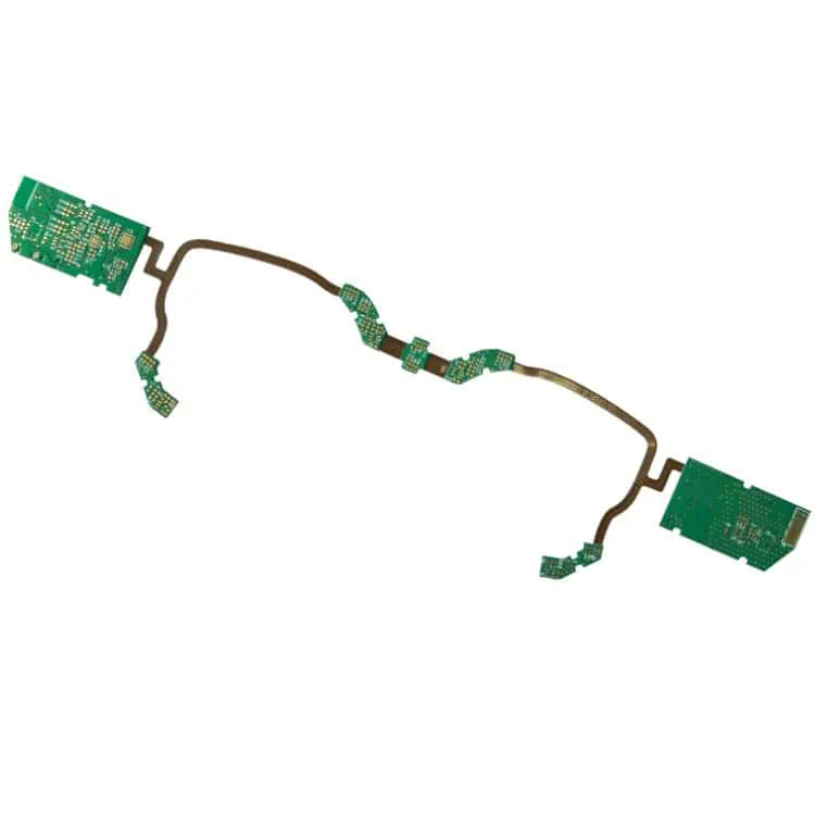
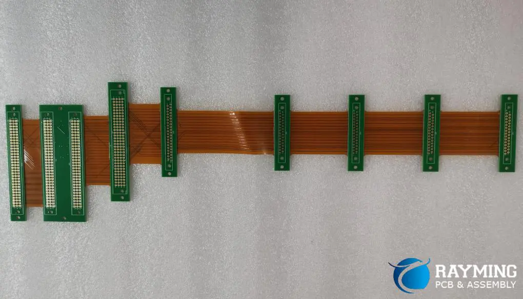
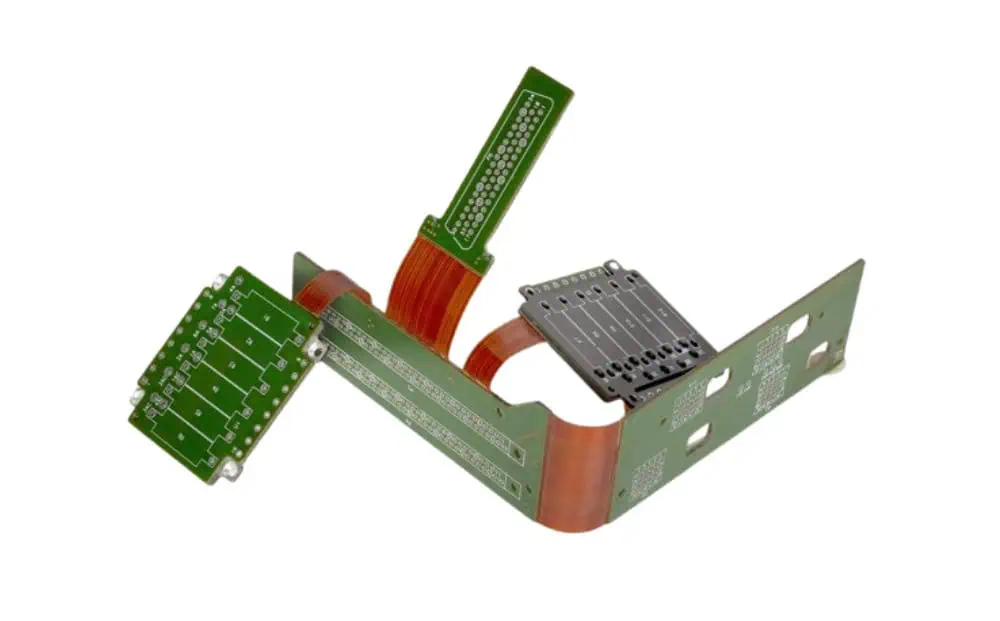
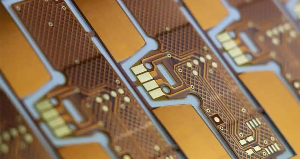
A Rigid-Flex PCB Stackup refers to the specific arrangement and composition of layers in a printed circuit board that incorporates both rigid and flexible sections. This unique construction allows for a seamless integration of traditional rigid board stability with the adaptability of flexible circuits. The proper design of a Rigid-Flex PCB Stackup is paramount in ensuring the reliability, performance, and manufacturability of advanced electronic devices.

YouTube video

As we delve deeper into this topic, we’ll explore the intricacies of Rigid-Flex PCB Stackup, addressing key challenges and uncovering the wealth of design opportunities it presents. Whether you’re an experienced PCB designer or new to the world of flexible circuits, understanding the nuances of Rigid-Flex PCB Stackup is essential for staying at the forefront of modern electronics design.

1. What Is a Rigid-Flex PCB Stackup?

Definition and Structure

A Rigid-Flex PCB Stackup is a specialized printed circuit board configuration that combines rigid and flexible circuit technologies within a single, integrated structure. This hybrid design consists of alternating layers of rigid and flexible materials, carefully arranged to meet specific mechanical and electrical requirements.

The rigid sections of the PCB provide stability and support for components, while the flexible sections allow for dynamic bending and folding. This unique combination enables designers to create complex three-dimensional layouts that can conform to tight spaces or unique form factors.

Advantages over Traditional Rigid Boards

Rigid-Flex PCB Stackups offer several significant advantages over conventional rigid PCBs:

  1. Space Optimization: By eliminating the need for connectors between separate rigid and flexible boards, Rigid-Flex designs can significantly reduce the overall size and weight of electronic assemblies.
  2. Increased Reliability: With fewer interconnection points, Rigid-Flex PCBs are less prone to connection failures, enhancing overall system reliability.
  3. Design Flexibility: The ability to bend and fold allows for creative solutions to packaging challenges, enabling designs that were previously impossible with rigid boards alone.
  4. Improved Signal Integrity: By reducing the number of connections and eliminating cables, Rigid-Flex designs can offer superior signal integrity, especially in high-frequency applications.
  5. Simplified Assembly: Rigid-Flex PCBs can reduce the complexity of assembly processes, potentially lowering manufacturing costs and improving quality control.

Typical Applications

The versatility of Rigid-Flex PCB Stackups has led to their adoption across a wide range of industries and applications:

  1. Medical Devices: Implantable devices, hearing aids, and portable diagnostic equipment benefit from the compact and flexible nature of Rigid-Flex designs.
  2. Aerospace and Defense: Satellites, aircraft avionics, and military communications systems utilize Rigid-Flex PCBs for their reliability and ability to withstand harsh environments.
  3. Consumer Electronics: Smartphones, wearable devices, and cameras leverage Rigid-Flex technology to achieve sleek, compact designs.
  4. Automotive: Advanced driver assistance systems (ADAS) and in-vehicle infotainment systems increasingly rely on Rigid-Flex PCBs to meet space constraints and reliability requirements.
  5. Industrial Equipment: Robotics, control systems, and test equipment benefit from the durability and design flexibility of Rigid-Flex stackups.

2. Key Elements of a Rigid-Flex Stackup Design

rigid flex pcb design

Designing an effective Rigid-Flex PCB Stackup requires a thorough understanding of its key elements. Each component plays a crucial role in the overall performance and reliability of the final product.

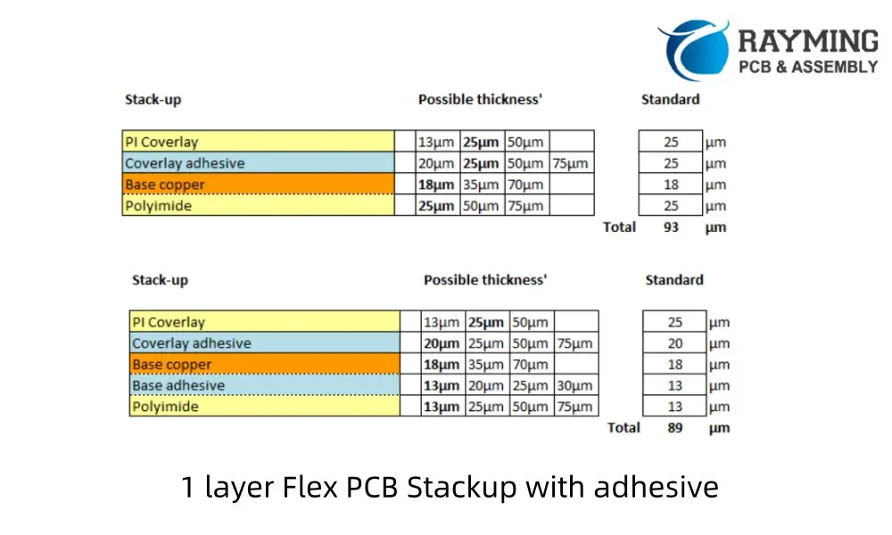
Flexible Core Materials

The flexible sections of a Rigid-Flex PCB are typically built around a core material that provides the necessary flexibility and electrical properties. The most common flexible core material is polyimide, known for its excellent mechanical and thermal stability. Key considerations for flexible core materials include:

  • Thickness: Ranging from 12.5ฮผm to 125ฮผm, depending on the required flexibility and electrical characteristics.
  • Copper Cladding: Available in various weights, typically from 1/2 oz to 2 oz per square foot.
  • Dimensional Stability: Important for maintaining consistent electrical properties across bending cycles.

Rigid Core Materials

The rigid sections of the PCB provide structural support and allow for the mounting of components. The most commonly used rigid core material is FR4, a glass-reinforced epoxy laminate. When selecting rigid core materials, consider:

  • Glass Transition Temperature (Tg): Higher Tg materials offer better thermal stability.
  • Coefficient of Thermal Expansion (CTE): Matching CTE between layers helps prevent delamination.
  • Dielectric Constant (Dk) and Loss Tangent: Critical for high-frequency applications.

Adhesives and Bonding Layers

Adhesives play a crucial role in bonding the rigid and flexible sections of the PCB. Common types include:

  • Acrylic Adhesives: Offer good flexibility and thermal resistance.
  • Epoxy Adhesives: Provide excellent bonding strength and chemical resistance.
  • No-Flow Prepregs: Used in more complex stackups to fill voids and provide insulation.

The choice of adhesive can significantly impact the overall performance and reliability of the Rigid-Flex PCB.

Coverlays vs. Solder Masks

In flexible circuit areas, coverlays are often used instead of traditional solder masks. Coverlays are typically made of polyimide film with an adhesive layer and offer several advantages:

  • Better flexibility and durability compared to liquid solder masks.
  • Improved protection against environmental factors.
  • Can be selectively applied to leave certain areas exposed for component mounting or interconnection.

In rigid sections, conventional solder masks are still used to protect copper traces and define soldering areas.

Importance of Controlled Impedance in Multilayer Designs

As Rigid-Flex PCBs often carry high-speed signals, maintaining controlled impedance throughout the design is crucial. This involves careful consideration of:

  • Trace Width and Spacing: Calculated based on the desired impedance and stackup characteristics.
  • Dielectric Thickness: Affects the capacitance between signal layers and ground planes.
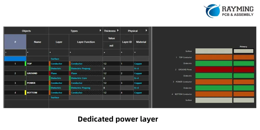
  • Ground Plane Placement: Strategic positioning of ground planes helps maintain consistent impedance and reduces EMI.

Designers must work closely with manufacturers to ensure that the intended impedance values can be achieved within manufacturing tolerances.

3. Multi-Layer Rigid-Flex PCB Stackup: Design Challenges

While Rigid-Flex PCB Stackups offer numerous advantages, they also present unique design challenges that must be carefully addressed to ensure optimal performance and reliability.

Layer Count and Complexity

As the number of layers in a Rigid-Flex PCB increases, so does the complexity of the stackup design. Designers must consider:

  • Balance Between Rigid and Flex Layers: Ensuring proper distribution of rigid and flexible layers to maintain overall board stability.
  • Neutral Axis Calculation: Positioning the flex layers near the neutral axis to minimize stress during bending.
  • Transition Zones: Carefully designing the areas where rigid sections transition to flexible sections to avoid stress concentration.

Mechanical Stress and Flex Cycles

One of the primary challenges in Rigid-Flex design is managing mechanical stress, particularly in areas that undergo repeated bending. Key considerations include:

  • Bend Radius: Determining the minimum bend radius to prevent damage to copper traces and dielectric materials.
  • Flex Cycle Life: Estimating the number of flex cycles the PCB can withstand before failure.
  • Strain Relief: Implementing proper strain relief techniques to distribute stress and prevent localized failures.

Signal Integrity and EMI Concerns

Maintaining signal integrity in Rigid-Flex designs can be challenging due to the varying dielectric properties between rigid and flexible sections. Designers must address:

  • Impedance Matching: Ensuring consistent impedance across rigid and flexible sections.
  • Cross-Talk: Minimizing electromagnetic coupling between adjacent traces, especially in tightly packed flexible sections.
  • EMI Shielding: Implementing effective shielding techniques, which may differ between rigid and flexible areas.

Importance of Accurate Rigid-Flex Stackup Modeling

Given the complexity of Rigid-Flex designs, accurate modeling of the PCB stackup is crucial. This involves:

  • 3D Modeling: Using advanced CAD tools to visualize and analyze the complete 3D structure of the Rigid-Flex PCB.
  • Material Property Simulation: Incorporating accurate material properties for both rigid and flexible sections in simulation models.
  • Thermal Analysis: Predicting heat distribution and potential hotspots, especially in areas where rigid and flexible sections meet.

4. Common Rigid Flex PCB Stackup Configurations

Rigid Flex PCB stackups come in various configurations to suit different application needs:

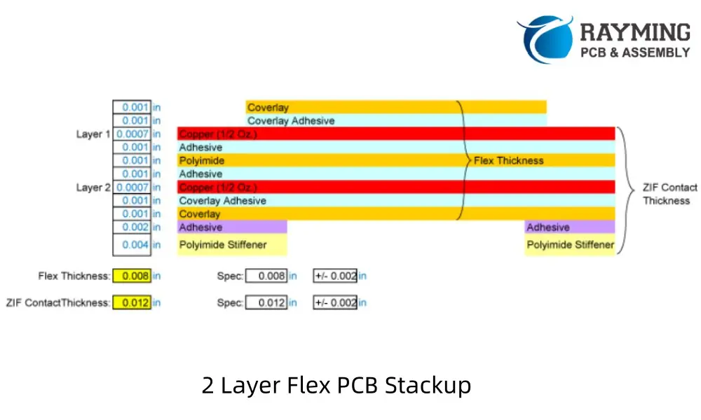
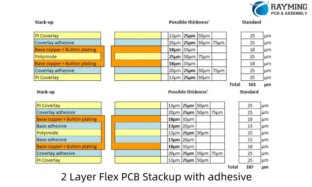
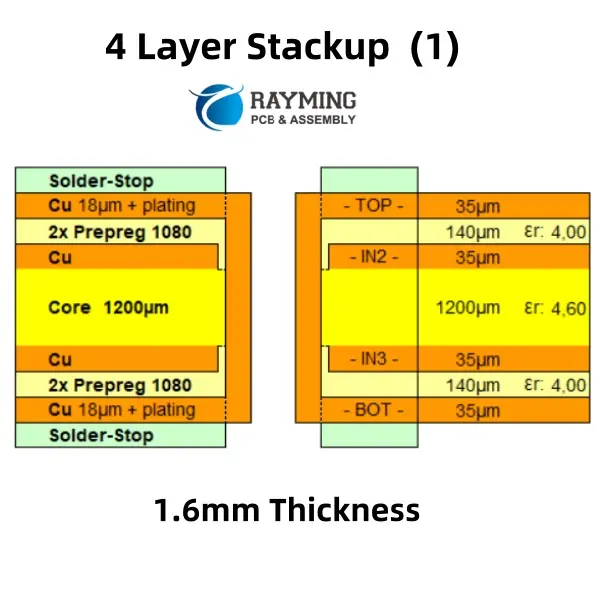
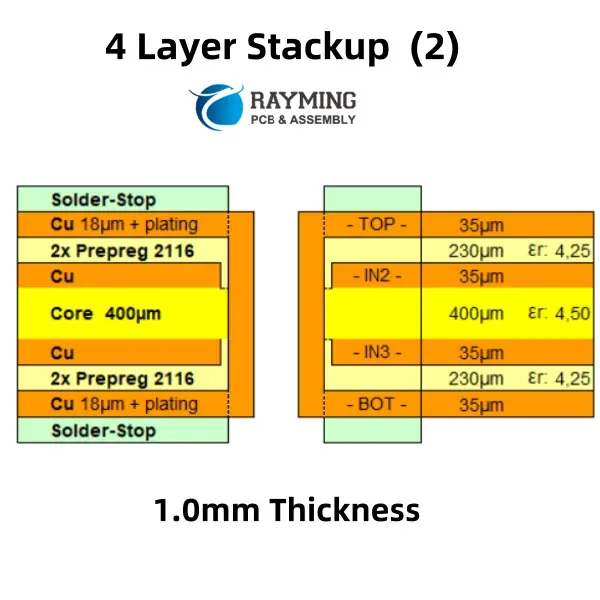
4 Layer Rigid Flex PCB Stack-up (2 Flex Layers)

A typical 4-layer Rigid-Flex PCB stackup with 2 flex layers consists of:

  1. Top solder mask
  2. Top copper layer (rigid)
  3. Prepreg
  4. Inner copper layer (flex)
  5. Flexible core
  6. Inner copper layer (flex)
  7. Prepreg
  8. Bottom copper layer (rigid)
  9. Bottom solder mask
4 Layer Rigid-Flex PCB Stack-up (2 Flex Layers)
4 Layer Rigid-Flex PCB Stack-up has four conductive

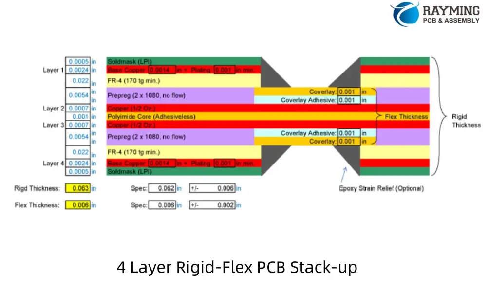
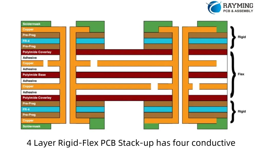
This configuration offers a good balance between flexibility and rigidity, suitable for applications requiring moderate complexity and bendability.

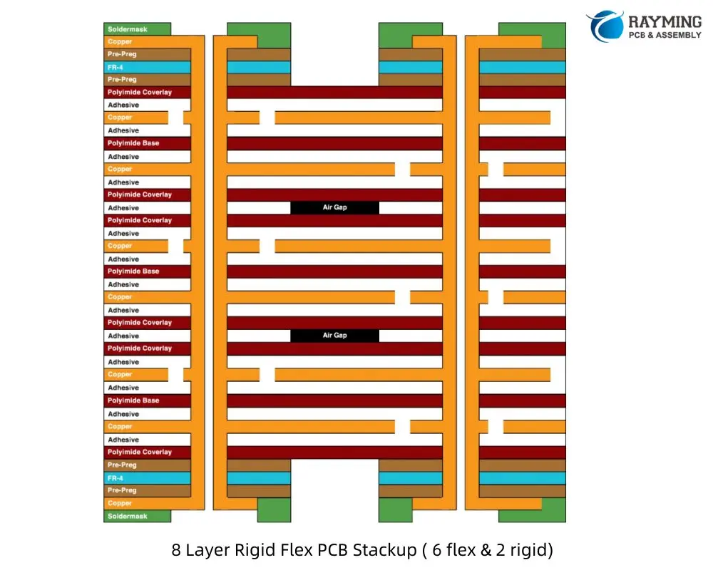
6 Layer Rigid Flex PCB Stackup (4 Flex Layers, 2 Rigid Layers with Air Gap)

A 6-layer Rigid-Flex PCB stackup with 4 flex layers and an air gap typically includes:

  1. Top solder mask
  2. Top copper layer (rigid)
  3. Prepreg
  4. Inner copper layer (flex)
  5. Flexible core
  6. Inner copper layer (flex)
  7. Flexible core
  8. Inner copper layer (flex)
  9. Flexible core
  10. Inner copper layer (flex)
  11. Air gap
  12. Prepreg
  13. Bottom copper layer (rigid)
  14. Bottom solder mask
6 Layer Rigid-Flex PCB Stack-up
6 Layer Rigid-Flex PCB Stack-up (4 flex and 2 rigid)
6 Layer Rigid-Flex PCB Stack-up (2 layer flex and 4 layer rigid)

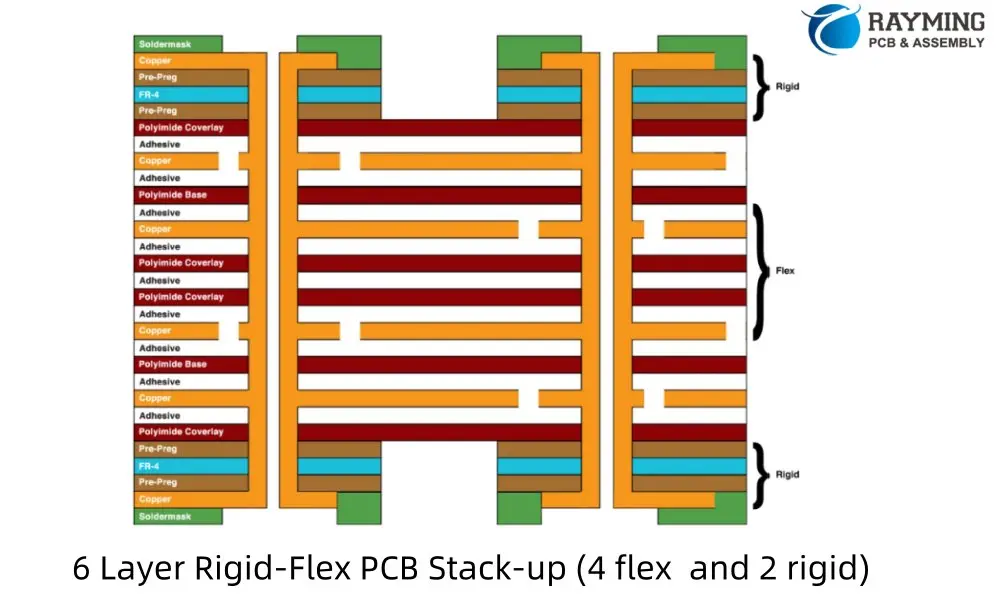
This design allows for increased circuit density in the flex portion while maintaining rigidity where needed. The air gap helps reduce overall thickness and improve flexibility.

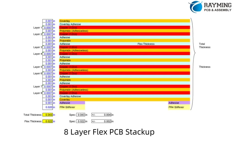
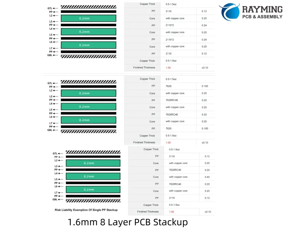
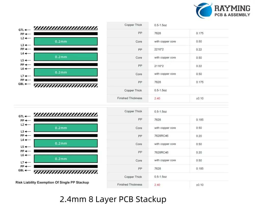
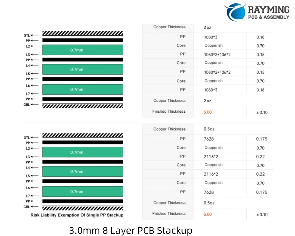
8 Layer Rigid Flex PCB Stackup (4 Flex Layers with Air Gap, 4 Rigid Layers)

An 8-layer Rigid-Flex PCB stackup with 4 flex layers, 4 rigid layers, and an air gap typically consists of:

  1. Top solder mask
  2. Top copper layer (rigid)
  3. Prepreg
  4. Inner copper layer (rigid)
  5. Core
  6. Inner copper layer (rigid)
  7. Prepreg
  8. Inner copper layer (flex)
  9. Flexible core
  10. Inner copper layer (flex)
  11. Flexible core
  12. Inner copper layer (flex)
  13. Flexible core
  14. Inner copper layer (flex)
  15. Air gap
  16. Prepreg
  17. Inner copper layer (rigid)
  18. Bottom copper layer (rigid)
  19. Bottom solder mask
8 Layer Rigid-Flex PCB Stack-up
8 Layer Rigid Flex PCB Stackup ( 6 layer flex & 2 layer rigid)

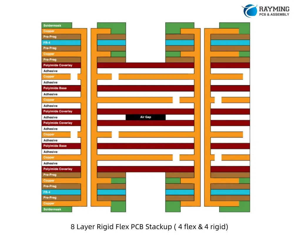
This configuration offers high circuit density in both rigid and flex sections, suitable for complex designs requiring significant routing capabilities.

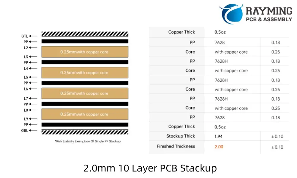
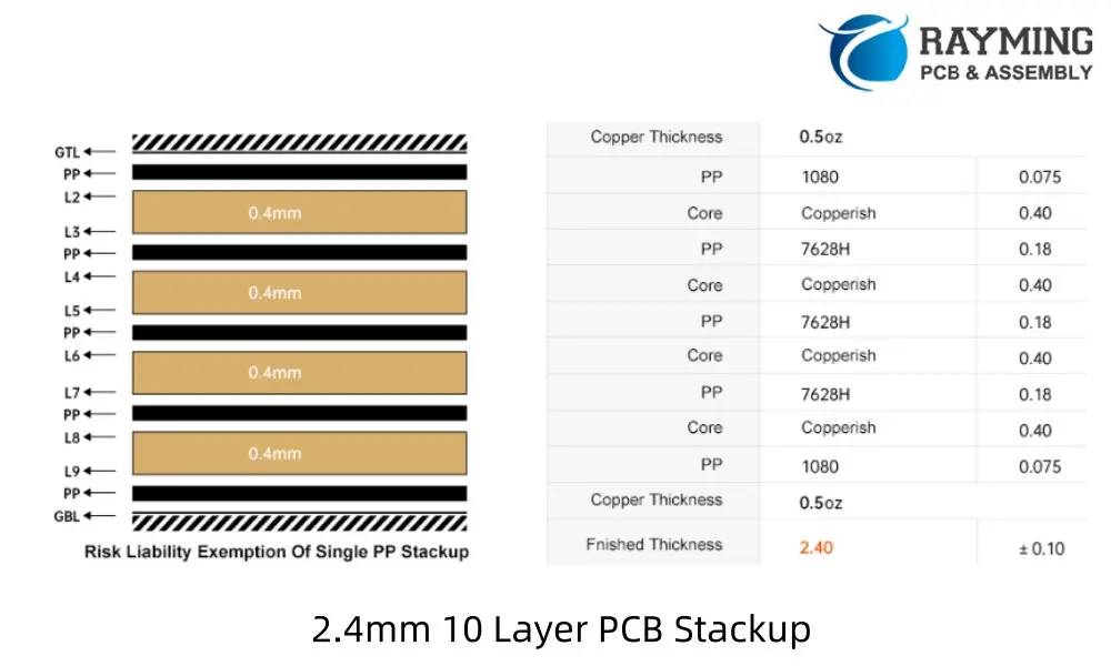
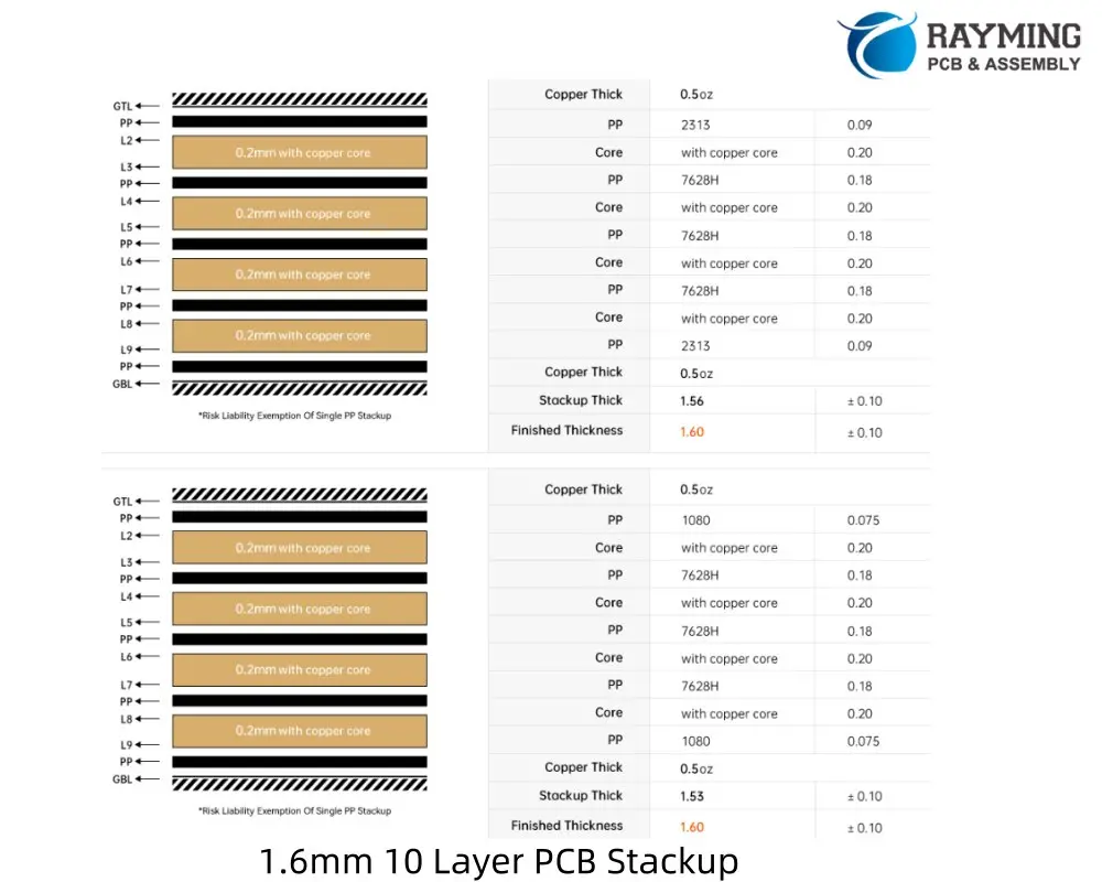
10 Layer Rigid-Flex PCB Stackup

A 10-layer Rigid-Flex PCB stackup typically includes:

  1. Top solder mask
  2. Top copper layer (rigid)
  3. Prepreg
  4. Inner copper layer (rigid)
  5. Core
  6. Inner copper layer (rigid)
  7. Prepreg
  8. Inner copper layer (rigid)
  9. Prepreg
  10. Inner copper layer (flex)
  11. Flexible core
  12. Inner copper layer (flex)
  13. Flexible core
  14. Inner copper layer (flex)
  15. Flexible core
  16. Inner copper layer (flex)
  17. Prepreg
  18. Inner copper layer (rigid)
  19. Core
  20. Inner copper layer (rigid)
  21. Bottom copper layer (rigid)
  22. Bottom solder mask
10 Layer Rigid Flex PCB Stackup

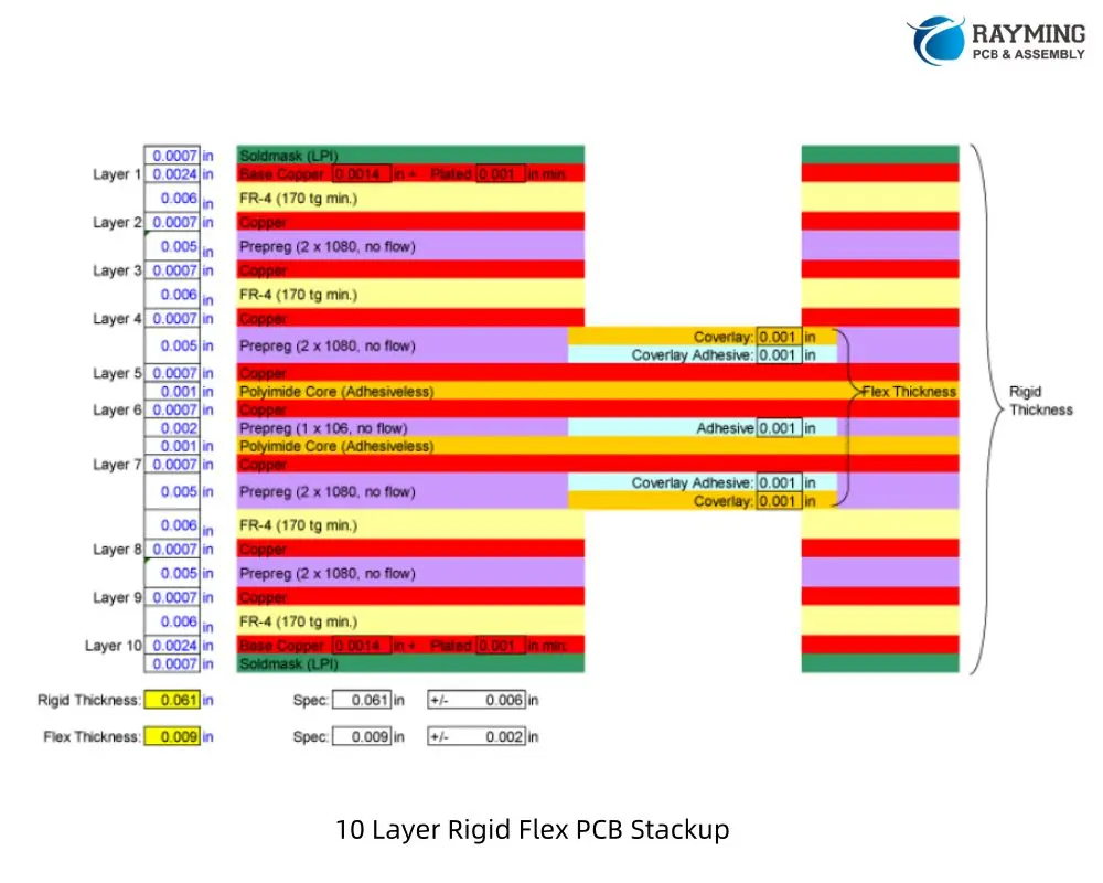
This design allows for very high circuit density and is suitable for complex applications requiring multiple ground and power planes in both rigid and flex sections.

12 Layer Rigid-Flex PCB Stackup (with Air Gap)

A 12-layer Rigid-Flex PCB stackup with an air gap might consist of:

  • Top solder mask
  • Top copper layer (rigid)
  • Prepreg
  • Inner copper layer (rigid)
  • Core
  • Inner copper layer (rigid)
  • Prepreg
  • Inner copper layer (rigid)
  • Core
  • Inner copper layer (rigid)
  • Prepreg
  • Inner copper layer (flex)
  • Flexible core
  • Inner copper layer (flex)
  • Flexible core
  • Inner copper layer (flex)
  • Flexible core
  • Inner copper layer (flex)
  • Air gap
  • Prepreg
  • Inner copper layer (rigid)
  • Core
  • Inner copper layer (rigid)
  • Prepreg
  • Inner copper layer (rigid)
  • Bottom copper layer (rigid)
  • Bottom solder mask
12 Layer Rigid Flex PCB Stackup

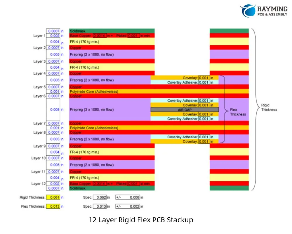
This configuration offers maximum circuit density and is ideal for the most complex Rigid-Flex applications. The air gap helps maintain flexibility in the flex portion despite the high layer count.

Read more about:

5. Using Altium Designer for Rigid-Flex Stackup Planning

Altium Designer is a powerful tool for creating Rigid-Flex PCB designs, offering specialized features to streamline the process. Here’s an overview of how to leverage Altium’s capabilities for effective stackup planning.

Overview of Altium Rigid-Flex Stackup Capabilities

Altium Designer provides a comprehensive set of tools for Rigid-Flex PCB design, including:

  • Layer Stack Manager: Allows detailed definition of both rigid and flexible sections.
  • Rigid-Flex Support: Enables the creation of complex board shapes with multiple rigid and flex areas.
  • 3D PCB Editor: Provides visualization of the folded PCB in its final form.

Setting Up Layer Stacks and Bending Zones

To set up a Rigid-Flex stackup in Altium:

  1. Use the Layer Stack Manager to define your base stackup.
  2. Create regions for different stackups (rigid and flex areas).
  3. Define bending lines to indicate where the board will flex.
  4. Specify bend radius and direction for each bending line.

Simulating Mechanical Bends

Altium’s 3D PCB Editor allows you to:

  • Visualize the PCB in its folded state.
  • Check for clearances and potential issues in the folded configuration.
  • Export 3D models for further analysis or integration with mechanical CAD systems.

Best Practices When Using Altium’s Rigid-Flex Tools

  1. Start with a well-planned stackup before beginning routing.
  2. Use the “Bend Region” feature to ensure proper clearances in flex areas.
  3. Leverage Altium’s Design Rule Checker to catch Rigid-Flex specific issues.
  4. Utilize the “Multi-board” feature for complex assemblies involving multiple Rigid-Flex boards.

Common Pitfalls to Avoid in Altium Designs

  1. Forgetting to define proper bend regions, leading to DRC errors.
  2. Incorrectly specifying layer functions in the stackup manager.
  3. Overlooking the need for different design rules in rigid vs. flex areas.
  4. Not utilizing the 3D viewer to check the folded configuration regularly during design.

6. Material Considerations for High-Reliability Rigid-Flex PCBs

The choice of materials plays a crucial role in the performance and longevity of Rigid-Flex PCBs, especially in high-reliability applications. Let’s explore the key material considerations.

Choosing the Right Flex Substrate

The flex substrate is the foundation of the flexible sections. Common options include:

  1. Polyimide (PI):
    • Pros: Excellent thermal stability, good chemical resistance.
    • Cons: Higher cost, can be brittle in extreme cold.
    • Best for: High-temperature applications, aerospace, and medical devices.
  2. Polyethylene Terephthalate (PET):
    • Pros: Lower cost, good flexibility.
    • Cons: Lower temperature resistance, less dimensional stability.
    • Best for: Consumer electronics, low-cost applications.
  3. Liquid Crystal Polymer (LCP):
    • Pros: Excellent electrical properties, low moisture absorption.
    • Cons: Higher cost, limited availability.
    • Best for: High-frequency applications, harsh environments.

Stiffener Materials and Placement

Stiffeners are used to provide additional support in specific areas of the flex circuit. Common materials include:

  • FR4: Compatible with rigid sections, good for component mounting areas.
  • Polyimide: Matches the flex substrate, useful for creating gradual transitions.
  • Aluminum: Provides excellent heat dissipation for high-power components.

Proper placement of stiffeners is crucial to manage stress and ensure reliability in dynamic flex applications.

Plated Through-Hole (PTH) Reliability

PTHs in flex circuits are particularly vulnerable to stress. To enhance reliability:

  • Use “via-in-pad” design where possible to reduce stress on the vias.
  • Consider buried or blind vias in rigid sections to minimize impact on flex areas.
  • Implement “anchoring” techniques to secure PTHs in flex regions.

Environmental Factors

High-reliability Rigid-Flex PCBs must withstand various environmental challenges:

  1. Temperature:
    • Choose materials with appropriate glass transition temperatures (Tg).
    • Consider coefficient of thermal expansion (CTE) matching between layers.
  2. Humidity:
    • Use moisture-resistant materials and coatings.
    • Implement proper sealing techniques for exposed flex areas.
  3. Chemicals:
    • Select materials with appropriate chemical resistance for the intended application.
    • Consider conformal coatings for additional protection.
  4. Mechanical Stress:
  • Design for the expected number of flex cycles.
  • Implement strain relief features in high-stress areas.

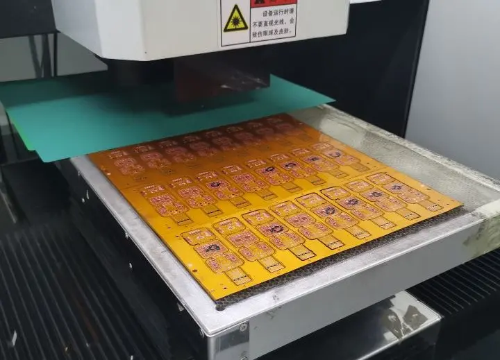
7. Manufacturing Insights: How Stackup Affects Fabrication

Understanding the manufacturing implications of your Rigid-Flex PCB stackup design is crucial for ensuring a successful and cost-effective production process. Let’s explore some key considerations.

Critical Manufacturing Constraints

  1. Layer Registration: As the number of layers increases, maintaining precise alignment becomes more challenging. Tight registration tolerances are essential, especially in flex areas.
  2. Material Handling: Flexible materials require special handling during manufacturing to prevent damage or distortion.
  3. Plating Processes: Achieving consistent plating across both rigid and flex areas can be challenging due to different material properties.
  4. Lamination: The lamination process must account for the different thermal and mechanical properties of rigid and flex materials.

Vias in Flex vs. Vias in Rigid Sections

Vias present unique challenges in Rigid-Flex PCBs:

  • Flex Sections: Vias in flex areas must withstand repeated bending. Laser-drilled microvias are often preferred for their smaller size and better reliability.
  • Rigid Sections: Traditional mechanical drilling is typically used, but care must be taken at the rigid-flex interface.
  • Stacked and Staggered Vias: These can be used to create reliable connections between layers while minimizing stress on the flex sections.

Panelization and Yield Considerations

Efficient panelization is crucial for optimizing yield and reducing costs:

  1. Panel Size: Consider the maximum panel size your manufacturer can handle, especially for larger flex circuits.
  2. Rigid-Flex Interface: Place rigid-flex transition areas away from panel edges to reduce stress during manufacturing.
  3. Scoring and Routing: Plan for appropriate methods to separate individual boards from the panel without damaging flex areas.
  4. Test Coupons: Include test coupons on the panel for quality control and impedance verification.

Working Closely with Your PCB Fabricator on Stackup Validation

Collaboration with your PCB manufacturer is essential for successful Rigid-Flex PCB production:

  1. Early Engagement: Involve your fabricator in the design process as early as possible to address manufacturability issues.
  2. Material Selection: Consult with your manufacturer on material availability and performance characteristics.
  3. Design Rule Verification: Ensure your design adheres to the manufacturer’s specific capabilities and limitations.
  4. Prototyping: Consider building prototypes to validate the design before moving to full production.

Conclusion

Mastering the intricacies of Rigid-Flex PCB stackup design is crucial for creating high-performance, reliable electronic products in today’s demanding markets. The ability to combine the stability of rigid boards with the flexibility of flex circuits opens up new possibilities in product design and functionality.

Key Takeaways:

  1. Precise Planning: Careful consideration of layer stackup, material selection, and mechanical design is essential for successful Rigid-Flex PCBs.
  2. Material Knowledge: Understanding the properties and interactions of various materials used in Rigid-Flex construction is crucial for optimal performance.
  3. Design Tools: Leveraging advanced PCB design software, like Altium Designer, can greatly simplify the complex task of Rigid-Flex layout and simulation.
  4. Manufacturing Awareness: Close collaboration with PCB fabricators and understanding of manufacturing constraints are vital for producing reliable Rigid-Flex boards.
  5. Continuous Learning: As technology evolves, staying updated on new materials, design techniques, and manufacturing processes is essential for innovation in Rigid-Flex PCB design.

Final Tips:

  • Prioritize early stackup planning to avoid costly redesigns later in the development process.
  • Utilize simulation tools to validate electrical and mechanical performance before committing to production.
  • Foster strong relationships with PCB manufacturers to leverage their expertise and capabilities.
  • Consider the entire product lifecycle, from assembly to field use, when making design decisions.

By embracing these principles and continuously refining your approach to Rigid-Flex PCB stackup design, you can create innovative, reliable, and high-performance electronic products that meet the demanding requirements of modern applications.

Appendix: Example Rigid-Flex Stackup Configurations

To further illustrate the concepts discussed in this article, here are some example Rigid-Flex PCB stackup configurations:

1. 4-Layer Rigid-Flex Stackup

Rigid Section:
    - Top Layer (Signal)
    - FR4 Core
    - Inner Layer 1 (Ground)
    - Flexible Polyimide Core
    - Inner Layer 2 (Power)
    - FR4 Core
    - Bottom Layer (Signal)

Flex Section:
    - Top Layer (Signal)
    - Adhesive
    - Inner Layer 1 (Ground)
    - Flexible Polyimide Core
    - Inner Layer 2 (Power)
    - Adhesive
    - Bottom Layer (Signal)

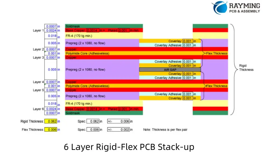
2. 6-Layer Rigid-Flex Stackup

Rigid Section:
    - Top Layer (Signal)
    - FR4 Prepreg
    - Inner Layer 1 (Signal)
    - FR4 Core
    - Inner Layer 2 (Ground)
    - Flexible Polyimide Core
    - Inner Layer 3 (Power)
    - FR4 Core
    - Inner Layer 4 (Signal)
    - FR4 Prepreg
    - Bottom Layer (Signal)

Flex Section:
    - Top Layer (Signal)
    - Adhesive
    - Inner Layer 1 (Signal)
    - Adhesive
    - Inner Layer 2 (Ground)
    - Flexible Polyimide Core
    - Inner Layer 3 (Power)
    - Adhesive
    - Inner Layer 4 (Signal)
    - Adhesive
    - Bottom Layer (Signal)

3. Complex Hybrid Stackup (8 Layers with Multiple Flex Layers)

Rigid Section:
    - Top Layer (Signal)
    - FR4 Prepreg
    - Inner Layer 1 (Signal)
    - FR4 Core
    - Inner Layer 2 (Ground)
    - Flexible Polyimide Core 1
    - Inner Layer 3 (Power)
    - Adhesive
    - Inner Layer 4 (Signal)
    - Flexible Polyimide Core 2
    - Inner Layer 5 (Ground)
    - FR4 Core
    - Inner Layer 6 (Signal)
    - FR4 Prepreg
    - Bottom Layer (Signal)

Flex Section:
    - Top Layer (Signal)
    - Adhesive
    - Inner Layer 1 (Signal)
    - Adhesive
    - Inner Layer 2 (Ground)
    - Flexible Polyimide Core 1
    - Inner Layer 3 (Power)
    - Adhesive
    - Inner Layer 4 (Signal)
    - Flexible Polyimide Core 2
    - Inner Layer 5 (Ground)
    - Adhesive
    - Inner Layer 6 (Signal)
    - Adhesive
    - Bottom Layer (Signal)

Tips for Custom Designs:

  1. Always consider the neutral bend axis when designing your stackup.
  2. Symmetry in the stackup can help reduce warping and twisting.
  3. Use thinner materials in flex areas to improve flexibility and reduce strain.
  4. Consider impedance requirements when choosing layer thicknesses and materials.
  5. Consult with your PCB manufacturer to ensure your design is feasible and cost-effective to produce.

Remember, these are general examples, and your specific design may require a custom stackup tailored to your unique requirements and constraints.

Flex PCB Stackup Design: Multi-Layer Strategies for Bendable Circuits

Flexible Printed Circuit Boards (Flex PCBs) have revolutionized electronic design, offering lightweight, space-saving solutions for various applications. Understanding the intricacies of Flex PCB stackup design is crucial for engineers and designers aiming to optimize their products. This article delves into the world of Flex PCB stackups, exploring configurations from 1 to 8 layers.

YouTube video

1. What is a Flex PCB Stackup?

Definition and Basics

A flex PCB stackup refers to the arrangement of conductive and insulating layers that make up a flexible printed circuit board. This layered structure is what allows the circuit to bend and flex while maintaining electrical integrity. The stackup design is crucial as it directly impacts the circuit’s mechanical properties, electrical performance, and overall reliability.

Differences Between Rigid, Flex, and Rigid-Flex PCB Stackups

While rigid PCBs are composed of stiff materials like FR-4, flex PCBs use flexible substrates that allow for bending and folding. The key differences are:

  1. Rigid PCBs: Typically use FR-4 or similar materials, with copper layers sandwiched between insulating layers. They’re inflexible and designed for static applications.
  2. Flex PCBs: Utilize flexible materials like polyimide for the base substrate, allowing the circuit to bend. They can have single or multiple layers.
  3. Rigid-Flex PCBs: Combine areas of rigid and flexible PCB technology on a single board, offering the best of both worlds for complex applications.

Key Materials Used in Flex PCB Stackups

The primary materials used in flex PCB stackups include:

  1. Polyimide: The most common base substrate for flex circuits, known for its excellent flexibility, heat resistance, and dimensional stability.
  2. Adhesive: Used to bond conductive layers to the substrate. Some advanced designs use adhesiveless constructions for improved flexibility and thermal performance.
  3. Coverlay: A protective layer applied over the outer copper layers, similar to solder mask on rigid PCBs but more flexible.
  4. Copper: The conductive material used for circuit traces, available in various weights to balance flexibility and current-carrying capacity.

Understanding these materials and their properties is essential for creating an optimal flex PCB stackup design.

2. Importance of Proper Flex PCB Layer Stackup

Balancing Mechanical Flexibility and Electrical Performance

One of the primary challenges in flex PCB stackup design is striking the right balance between mechanical flexibility and electrical performance. A well-designed stackup must:

  1. Allow for the required degree of flexing without damaging the circuit.
  2. Maintain signal integrity across bending regions.
  3. Provide adequate shielding and impedance control for high-speed signals.

Achieving this balance often involves careful material selection, layer ordering, and thickness considerations.

Impact on Bend Radius, Durability, and Signal Integrity

The stackup design directly affects the circuit’s minimum bend radius โ€“ the smallest curve the PCB can conform to without damage. A properly designed stackup can:

  1. Minimize stress on copper traces during flexing.
  2. Reduce the risk of delamination or cracking in dynamic applications.
  3. Maintain consistent electrical characteristics even when bent.

For instance, placing signal layers closer to the neutral axis (the center of the stackup) can reduce strain during bending, improving durability.

How Flex Circuit Stackup Affects Product Lifespan

The longevity of a flexible circuit is intrinsically tied to its stackup design. A well-engineered stackup can significantly extend a product’s lifespan by:

  1. Reducing mechanical stress on components and solder joints.
  2. Minimizing signal degradation over time due to repeated flexing.
  3. Improving resistance to environmental factors like temperature fluctuations and humidity.

3. Typical Flex PCB Stackup Structures

Flex PCB stackups refer to the arrangement of conductive layers, insulating materials, and other elements that make up a flexible circuit board. The design of these stackups is critical in determining the board’s performance, flexibility, and reliability.

1 Layer Flex PCB Stackup

The simplest form of Flex PCB, a single-layer design consists of:

  1. Coverlay (optional)
  2. Single conductive layer (usually copper)
  3. Flexible base material (e.g., Polyimide)
  4. Coverlay (optional)
1 Layer Flex PCB Stackup with FR-4 Stiffener
1 layer Flex PCB Stackup with adhesive

This configuration is ideal for simple circuits with low component density. It offers maximum flexibility and is cost-effective for basic applications.

Read more about:

2 Layer Flex PCB Stackup

A 2-layer Flex PCB stackup typically includes:

  1. Coverlay
  2. Conductive layer
  3. Flexible base material
  4. Conductive layer
  5. Coverlay
2 Layer Flex PCB Stackup with ZIP Contact fingers

This design allows for more complex circuits while maintaining good flexibility. It’s commonly used in applications requiring ground planes or power distribution.

4 Layer Flex PCB Stackup

A 4-layer Flex PCB stackup usually consists of:

  1. Coverlay
  2. Conductive layer
  3. Flexible base material
  4. Conductive layer
  5. Flexible base material
  6. Conductive layer
  7. Flexible base material
  8. Conductive layer
  9. Coverlay
4 Layer Flex PCB Stackup with adhesive

This configuration offers increased circuit density and improved signal integrity. It’s suitable for applications requiring separation of analog and digital signals or complex routing.

6 Layer Flex PCB Stackup

A typical 6-layer Flex PCB stackup includes:

  1. Coverlay
  2. Conductive layer
  3. Flexible base material
  4. Conductive layer
  5. Flexible base material
  6. Conductive layer
  7. Flexible base material
  8. Conductive layer
  9. Flexible base material
  10. Conductive layer
  11. Flexible base material
  12. Conductive layer
  13. Coverlay
6 Layer Flex PCB Stackup

This design allows for high component density and is ideal for complex circuits requiring multiple ground and power planes. It offers excellent signal integrity but with reduced flexibility compared to lower layer counts.

8 Layer Flex PCB Stackup

An 8-layer Flex PCB stackup typically consists of:

  1. Coverlay
  2. Conductive layer
  3. Flexible base material
  4. Conductive layer
  5. Flexible base material
  6. Conductive layer
  7. Flexible base material
  8. Conductive layer
  9. Flexible base material
  10. Conductive layer
  11. Flexible base material
  12. Conductive layer
  13. Flexible base material
  14. Conductive layer
  15. Flexible base material
  16. Conductive layer
  17. Coverlay
8 Layer Flex PCB Stackup

This configuration is used for the most complex flex circuits, offering maximum circuit density and signal integrity. However, it has the least flexibility among the options discussed.

4. 4 Layer Flex PCB Stackup: Advanced Designs

Common Architecture for 4 Layer Flex PCB Stackup

A typical 4 layer flex PCB stackup might be structured as follows:

  1. Top coverlay
  2. Signal layer 1
  3. Ground plane
  4. Power plane
  5. Signal layer 2
  6. Bottom coverlay

This arrangement allows for optimal signal integrity and power distribution while maintaining flexibility.

Importance of Symmetrical Stackup for Dynamic Flexing

Symmetry in the stackup design is crucial for dynamic flexing applications. A symmetrical design:

  1. Balances stress across the layers during bending
  2. Reduces the risk of warping or twisting
  3. Maintains consistent electrical properties in different flex states

To achieve symmetry, designers often mirror the stackup around the central core, using similar materials and thicknesses on both sides.

Via Management and Controlled Impedance Considerations

In 4 layer flex PCB stackups, via management becomes more complex. Some key considerations include:

  1. Minimizing via use in flex areas to maintain bendability
  2. Using buried or blind vias to increase routing density without compromising flexibility
  3. Implementing teardrops at via-to-trace connections to improve reliability

Controlled impedance is often a requirement in high-speed designs. In a 4 layer stackup, designers can:

  1. Use the inner layers for uninterrupted ground and power planes
  2. Adjust trace width and spacing on outer layers to achieve desired impedance
  3. Utilize electromagnetic field simulation tools to fine-tune impedance control

5. Special Considerations for Flex Stackup Design

How to Minimize Stress and Avoid Cracking

To ensure the longevity of flex PCBs, designers must minimize stress on the copper traces and substrate. Key strategies include:

  1. Using rolled annealed copper instead of electrodeposited copper for better flex endurance
  2. Implementing teardrop-shaped pads to reduce stress concentration
  3. Orienting traces perpendicular to the bend axis in flex areas
  4. Using smaller trace widths in areas of high stress

Coverlay vs. Soldermask Choice in Flex Stackup

While rigid PCBs typically use soldermask, flex PCBs often employ coverlay for outer layer protection. The choice between coverlay and soldermask depends on several factors:

Coverlay Advantages:

  • Better flexibility and durability
  • Excellent chemical resistance
  • Uniform thickness for improved impedance control

Soldermask Advantages:

  • Lower cost
  • Easier application in small areas
  • Better for fine-pitch components

For dynamic flex applications, coverlay is generally preferred due to its superior flexibility and durability.

Adhesiveless Constructions

Adhesiveless flex PCB constructions are gaining popularity due to several advantages:

  1. Improved flexibility and bend radius capabilities
  2. Better thermal performance
  3. Reduced overall thickness
  4. Enhanced electrical performance due to lower dielectric constant

However, adhesiveless constructions can be more challenging to manufacture and may have higher initial costs. The choice between adhesive-based and adhesiveless constructions should be based on the specific requirements of the application.

6. Tools and Resources for Flex Circuit Stackup Design

How Altium Flex Stackup Tools Assist with Design Simulation

Altium Designer, a popular PCB design software, offers powerful tools for flex PCB stackup design and simulation. Key features include:

  1. Layer Stack Manager: Allows designers to define and visualize the PCB stackup, including flex layers.
  2. Flex and Rigid-Flex Support: Enables the definition of flex and rigid regions within the same design.
  3. 3D PCB Visualization: Helps in understanding how the flex PCB will behave in its bent state.
  4. Signal Integrity Analysis: Allows for impedance calculations and signal integrity simulations specific to flex designs.

Typical Workflow: Setting Bend Parameters, Defining Flex Regions

A typical workflow for flex PCB design in Altium might include:

  1. Define the overall stackup using the Layer Stack Manager.
  2. Specify flex and rigid regions using the Rigid-Flex Editor.
  3. Set bend lines and bend parameters (e.g., bend radius, bend angle).
  4. Route traces with consideration for bend regions.
  5. Perform design rule checks specific to flex PCBs.
  6. Run signal integrity simulations to ensure performance in both flat and bent states.
  7. Generate 3D models and documentation for manufacturing.

By leveraging these tools, designers can catch potential issues early in the design process, saving time and reducing the risk of costly revisions.

7. Manufacturer-Specific Stackups: PCBWay Flex PCB Stackup Options

Overview of PCBWay Flex Stackup Capabilities

PCBWay, a leading PCB manufacturer, offers a wide range of flex PCB stackup options to cater to diverse design requirements. Their capabilities include:

  1. Single-layer to multi-layer flex PCBs (up to 8 layers)
  2. Various substrate materials, including polyimide and PET
  3. Different copper weights (0.5oz to 2oz)
  4. Adhesive-based and adhesiveless constructions
  5. Coverlay and soldermask options

PCBWay’s advanced manufacturing processes allow for:

  • Minimum trace width/spacing down to 3mil/3mil
  • Laser-drilled microvias for high-density designs
  • Selective stiffener application for hybrid flex-rigid designs

Tips on Communicating with Manufacturers about PCBWay Flex PCB Stackup Requirements

Effective communication with manufacturers like PCBWay is crucial for successful flex PCB production. Here are some tips:

  1. Provide Detailed Stackup Information:
    • Clearly specify layer count, materials, and thicknesses
    • Indicate which layers are flexible and which (if any) are rigid
  2. Define Bend Requirements:
    • Specify minimum bend radius
    • Indicate whether the flex is for dynamic or static applications
  3. Clarify Special Requirements:
    • Controlled impedance needs
    • Any specific material preferences (e.g., adhesiveless construction)
  4. Supply Detailed Documentation:
    • Provide Gerber files, drill files, and fabrication drawings
    • Include a readme file with any special instructions or requirements
  5. Discuss Prototyping Options:
    • Consider ordering prototypes before full production
    • Discuss any testing or validation requirements
  6. Leverage Manufacturer Expertise:
    • Ask for recommendations on improving manufacturability
    • Inquire about alternative materials or processes that might enhance performance or reduce cost

By following these guidelines, you can ensure that your flex PCB design intent is clearly communicated, leading to a smoother manufacturing process and a higher-quality end product.

8. Best Practices for a Reliable Flex PCB Stackup

Layer Symmetry

Maintaining symmetry in the flex PCB stackup is crucial for preventing warpage and ensuring consistent performance. Best practices include:

  1. Balancing copper weights on both sides of the core
  2. Mirroring layer structures around the central core
  3. Using an odd number of layers with a central ground plane for better EMI performance

Proper Material Selection

Choosing the right materials is fundamental to a successful flex PCB design:

  1. Substrate: Polyimide is the most common choice due to its excellent flexibility and temperature resistance. For less demanding applications, PET might be suitable.
  2. Copper Foil: Rolled annealed copper offers better flex endurance than electrodeposited copper.
  3. Adhesives: Choose adhesives that maintain flexibility over the product’s lifetime and temperature range.
  4. Coverlay: Select a coverlay material that matches the flexibility of your substrate.

Bend Area Design Rules

Optimizing the design for bend areas is critical for long-term reliability:

  1. Route traces perpendicular to the bend line whenever possible.
  2. Use smaller trace widths in bend areas to reduce stress.
  3. Avoid placing vias or components directly in bend zones.
  4. Implement teardrop-shaped pads to reduce stress concentration.
  5. Consider using curved traces instead of sharp corners in high-stress areas.

Controlled Impedance for High-Speed Signals

For high-speed applications, maintaining controlled impedance is crucial:

  1. Use continuous ground planes adjacent to signal layers.
  2. Carefully calculate and maintain consistent trace width and spacing.
  3. Consider using impedance-controlled microstrip or stripline configurations.
  4. Use electromagnetic simulation tools to verify impedance control across bend areas.

By adhering to these best practices, designers can create flex PCB stackups that offer optimal performance, reliability, and manufacturability.

9. Conclusion

The world of flexible electronics continues to expand, pushing the boundaries of what’s possible in product design and functionality. At the heart of this revolution lies the critical importance of a well-designed flex PCB stackup. As we’ve explored throughout this article, the stackup is not merely a technical specification but the foundation upon which reliable, high-performance flexible circuits are built.

From single-layer designs to complex multi-layer architectures, each flex PCB stackup presents unique challenges and opportunities. By understanding the fundamental principles of stackup design โ€“ from material selection and layer

Standard 10 Layer PCB Stack-up Design Reference

Introduction

A 10-layer PCB stack-up offers a balance between complexity and performance for advanced electronic applications. This guide provides key information on composition, advantages, considerations, and common configurations for 10-layer PCBs.

10-Layer <a href="https://www.raypcb.com/how-to-plan-multilayer-pcb-stackup/">PCB Stackup</a> Selector

10-Layer PCB Stackup Selector 10L

Configure layer thicknesses for advanced 10-layer HDI PCB designs

Quick Presets

Layer Assignment
L1 SIG
L2 GND
L3 SIG
L4 PWR
L5 SIG
L6 SIG
L7 GND
L8 SIG
L9 PWR
L10 SIG

Copper Layers

Prepreg Layers (5)

Core Layers (4)

Total Board Thickness
1.600mm
1600 ยตm
vs 1.6mm
+0 ยตm
Copper (10L)
350 ยตm
Prepreg (5L)
642 ยตm
Core (4L)
600 ยตm

Stackup Visualization

L1 – Top SignalSIG 35ยตm
Prepreg 1 (PP1) 114ยตm
L2 – GND PlaneGND 35ยตm
Core 1 (FR-4) 100ยตm
L3 – Inner SignalSIG 35ยตm
Prepreg 2 (PP2) 114ยตm
L4 – PWR PlanePWR 35ยตm
Core 2 (FR-4) 200ยตm
L5 – Inner SignalSIG 35ยตm
Prepreg 3 (PP3) – Center 185ยตm
L6 – Inner SignalSIG 35ยตm
Core 3 (FR-4) 200ยตm
L7 – GND PlaneGND 35ยตm
Prepreg 4 (PP4) 114ยตm
L8 – Inner SignalSIG 35ยตm
Core 4 (FR-4) 100ยตm
L9 – PWR PlanePWR 35ยตm
Prepreg 5 (PP5) 114ยตm
L10 – Bottom SignalSIG 35ยตm
SOLDER MASK (BOTTOM)
Outer Signal
Inner Signal
GND Plane
PWR Plane
Prepreg
Core
๐Ÿ’ก Common 10-Layer Targets
1.2mm: High-density mobile, FPGA applications
1.6mm: Standard multilayer (most common)
2.0mm: Industrial, server boards
2.4mm – 3.0mm: Backplanes, heavy copper
โšก 10-Layer Design Strategy
Symmetric Structure: L1-L5 mirrors L6-L10 for balanced warpage control.
High-Speed Routing: L3, L5, L6, L8 are stripline layers with excellent shielding.
Power Integrity: Distributed GND (L2, L7) and PWR (L4, L9) minimize loop inductance.
๐Ÿ“ Impedance Reference
L1 & L10: Microstrip (ref: L2, L9)
L3: Stripline (ref: L2 + L4)
L5 & L6: Broadside-coupled stripline
L8: Stripline (ref: L7 + L9)

Basic Structure

Typical arrangement of layers in a 10-layer stack-up PCB:

  1. Top Layer (Signal)
  2. Prepreg
  3. Signal Layer 1
  4. Core
  5. Internal Power/Ground Plane 1
  6. Prepreg
  7. Signal Layer 2
  8. Core
  9. Internal Power/Ground Plane 2
  10. Prepreg
  11. Signal Layer 3
  12. Core
  13. Internal Power/Ground Plane 3
  14. Prepreg
  15. Signal Layer 4
  16. Core
  17. Internal Power/Ground Plane 4
  18. Prepreg
  19. Bottom Layer (Signal)

Advantages of 10-Layer Stack-Ups

  • Enhanced design flexibility
  • Improved signal integrity
  • Enhanced power distribution
  • Suitable for high-density designs
  • Cost-effective compared to higher-layer configurations
YouTube video

Design Considerations

  • Signal integrity management
  • Controlled impedance requirements
  • Complex routing paths
  • Manufacturing and fabrication costs
  • Proper trace widths and layer ordering

Common 10-Layer PCB Stack-up Configurations

1 Standard Stack-Up

  • Alternating signal and power/ground layers
  • Balanced design for general-purpose applications

2 Mixed Signal Stack-Up

  • Separation of analog and digital signals
  • Improved isolation between different signal types

3 High-Speed Signal Stack-Up

  • Dedicated layers for high-speed signals
  • Enhanced signal integrity for critical paths

4 Power Integrity Stack-Up

  • Multiple power planes for improved power distribution
  • Reduced voltage drops and noise

5 Buried Capacitance Stack-Up

  • Embedded capacitance layers
  • Improved power delivery and reduced EMI

10 Layer PCB Stackup reference for different thickness:

2.0mm 10 Layer PCB Stackup
2.4mm 10 Layer PCB Stackup
1.6mm 10 Layer PCB Stackup

Design Guidelines

  1. Separate high-speed signals from noise-sensitive circuits
  2. Use ground planes adjacent to critical signal layers
  3. Implement proper via management for layer transitions
  4. Maintain consistent impedance across layers
  5. Consider crosstalk between adjacent signal layers
  6. Optimize power distribution network (PDN) design
  7. Implement proper EMI/EMC shielding techniques

Impedance Control

  • Use impedance calculation tools for accurate trace dimensions
  • Consider dielectric constant and thickness of materials
  • Maintain consistent trace widths for controlled impedance

Manufacturing Considerations

  • Verify manufacturer capabilities for 10-layer production
  • Discuss special requirements (e.g., buried vias, impedance control)
  • Consider cost implications of complex designs

Conclusion

A well-designed 10-layer PCB stack-up offers enhanced performance and flexibility for complex electronic designs. Careful consideration of signal integrity, power distribution, and EMC requirements is crucial for successful implementation. Use this guide as a starting point, and consult with PCB design experts and manufacturers for specific project requirements.

If you need stackup suggestion for your 10 layer PCB design, welcome to send email to Sales@raypcb.com .

Standard 8 Layer PCB Stackup Design and Suggestion

As electronic devices become smaller and signal speeds increase, multilayer PCBs have become increasingly important. Among these, the 8-layer PCB stackup offers a balance between complexity and performance for many advanced applications. This article explores the reasons for using an 8-layer PCB, its typical structure, and best practices for design.

Why Use a Standard 8 Layer PCB Stackup?

  1. Space Efficiency: With at least 4 layers for signal traces, more space is available on outer layers for components.
  2. Improved Signal Integrity: Power and ground planes between signal layers reduce crosstalk.
  3. Better EMI Control: Multiple layers allow for better electromagnetic interference (EMI) management.
  4. Thermal Management: Increased layers provide more options for heat distribution.
8-Layer PCB Stackup Selector

8-Layer PCB Stackup Selector 8L

Configure layer thicknesses for high-density 8-layer PCB designs

Quick Presets

Copper Layers

Prepreg Layers

Core Layers

Total Board Thickness
1.600mm
1600 ยตm
vs 1.6mm
+0 ยตm
Copper (8L)
280 ยตm
Prepreg (4L)
598 ยตm
Core (3L)
600 ยตm

Stackup Visualization

L1 – Top SignalSIG 35ยตm
Prepreg 1 (PP1) 114ยตm
L2 – GND PlaneGND 35ยตm
Core 1 (FR-4) 200ยตm
L3 – Inner SignalSIG 35ยตm
Prepreg 2 (PP2) 185ยตm
L4 – PWR PlanePWR 35ยตm
Core 2 – Center (FR-4) 200ยตm
L5 – GND PlaneGND 35ยตm
Prepreg 3 (PP3) 185ยตm
L6 – Inner SignalSIG 35ยตm
Core 3 (FR-4) 200ยตm
L7 – PWR PlanePWR 35ยตm
Prepreg 4 (PP4) 114ยตm
L8 – Bottom SignalSIG 35ยตm
SOLDER MASK (BOTTOM)
Outer Signal
Inner Signal
GND Plane
PWR Plane
Prepreg
Core
๐Ÿ’ก Common 8-Layer Targets
1.0mm: High-density mobile/wearable
1.6mm: Standard multilayer (most common)
2.0mm: Industrial, automotive
2.4mm: Power systems, thick copper
โšก 8-Layer Design Tips
Signal Integrity: L3 & L6 are shielded by adjacent planes – ideal for high-speed signals.
Power Distribution: L4 & L5 form a tightly-coupled power/ground pair – excellent for decoupling.
๐Ÿ“ Impedance Control
Outer layers (L1, L8): Microstrip impedance
Inner layers (L3, L6): Stripline impedance
Adjust PP thickness to tune impedance values.

Typical Structure of an 8 Layer PCB Stackup

A standard 8-layer PCB stackup usually consists of the following layers:

  1. Top Layer (Signal)
  2. Prepreg
  3. Ground Plane
  4. Core
  5. Inner Layer 1 (Signal)
  6. Prepreg
  7. Power Plane
  8. Core
  9. Ground Plane
  10. Prepreg
  11. Inner Layer 2 (Signal)
  12. Core
  13. Power Plane
  14. Prepreg
  15. Bottom Layer (Signal)

This arrangement separates signal layers with power or ground planes to reduce EMI susceptibility and emission.

YouTube video

Design Techniques and Challenges

1. Routing Direction

  • Route signal traces on adjacent layers perpendicularly to minimize crosstalk.
  • Maintain different routing directions on subsequent layers, even when separated by power or ground planes.

2. Return Path

  • Visualize and optimize the return path for high-speed signals, even on inner layers.
  • Ensure short return paths to minimize interference with other components.

3. Ground Plane Management

  • Avoid split ground planes to prevent impedance discontinuities.
  • Ensure low-impedance connections from outer layer components to inner ground planes via vias.

4. Via Usage

  • Consider using buried or blind vias to increase routing space.
  • Verify manufacturer capabilities for producing complex via structures.

5. Material Selection

  • Choose appropriate prepreg and core materials.
  • Consider how material properties affect impedance control for transmission line design.

6. Manufacturer Capabilities

  • Ensure your PCB manufacturer can produce the specified 8-layer stackup.
  • Discuss any special requirements, such as impedance control or via structures, with your manufacturer.

8 Layer PCB Stackup reference for different thickness design

1.2mm 8 Layer PCB Stackup
1.6mm 8 Layer PCB Stackup

Conclusion

While an 8-layer PCB stackup offers numerous advantages, it also presents unique challenges. Adhering to best practices and using appropriate design tools are crucial for success. Remember that an 8-layer stackup isn’t a universal solution to all EMI problems โ€“ proper design techniques remain essential.

Designers should leverage advanced PCB design software, such as OrCAD PCB Designer, which offers features like Cross Section Editor for layer stackup control, strong DRC tools, and reliable analysis and simulation capabilities. These tools can significantly simplify the complex task of designing an 8-layer PCB.

If you need Stackup suggestion for your 8 layer PCB design, Welcome to send email to sales@raypcb.com .

6 Layer PCB Stackup Design Guidelines and Reference

24 layer pcb

Why Upgrade to 6 Layers?

When a 4-layer PCB no longer suffices, it’s time to consider a 6-layer board. The additional layers offer several benefits:

  1. More signal routing space
  2. An extra plane pair
  3. Flexibility in conductor arrangement

The key to success lies in the PCB stackup arrangement and routing strategy.

6-Layer PCB Stackup Selector

6-Layer PCB Stackup Selector 6L

Configure layer thicknesses for your 6-layer PCB stackup

Copper Layers

Prepreg Layers

Core Layers

Total Board Thickness
1.200mm
1200 ยตm
vs 1.2mm target: +0 ยตm
Component Thickness
Copper (6 layers) 210 ยตm
Prepreg (3 layers) 456 ยตm
Core (2 layers) 400 ยตm

Stackup Visualization

L1 – Top SignalOUTER 35ยตm
Prepreg 1 (PP1) 114ยตm
L2 – GND PlanePLANE 35ยตm
Core 1 (FR-4) 200ยตm
L3 – Inner SignalSIGNAL 35ยตm
Prepreg 2 (PP2) 228ยตm
L4 – Inner SignalSIGNAL 35ยตm
Core 2 (FR-4) 200ยตm
L5 – PWR PlanePLANE 35ยตm
Prepreg 3 (PP3) 114ยตm
L6 – Bottom SignalOUTER 35ยตm
SOLDER MASK (BOTTOM)
Outer Copper
Plane (GND/PWR)
Inner Signal
Prepreg (PP)
Core (FR-4)
Solder Mask
๐Ÿ’ก Common 6-Layer Targets
1.0mm: High-density, compact designs
1.2mm: Standard thin multilayer
1.6mm: Most common thickness
2.0mm: Power applications, thermal management
โšก Layer Arrangement Tips
L2 (GND) & L5 (PWR): Place planes adjacent to outer signal layers for better impedance control and EMI shielding.
L3 & L4: Inner signal layers – route high-speed signals here for protection.

Reasons to Choose a 6-Layer Board

  1. More surface space: Moving power and signal layers inside frees up room for components on the surface.
  2. Mixed-signal boards: Dedicate a surface layer to analog interfaces and use an internal layer for slower digital routing.
  3. High-speed, high I/O count boards: Separate signals into different layers for better organization.

Typical 6-Layer PCB Stackup

A common 6-layer stackup arrangement:

  1. Signal (Top)
  2. Ground
  3. Power
  4. Signal
  5. Ground
  6. Signal (Bottom)

Signal Routing Guidelines

  • Use top and bottom layers for impedance-controlled signals.
  • Thin dielectrics (โ‰ค10 mil) are preferable for these outer layers.
  • For digital interfaces with differential pairs, reduced trace width allows routing to fine-pitch components.

Power Routing Strategies

  • Dedicate an internal layer to power distribution.
  • Break up the power plane into rails for multiple voltages if needed.
  • You can still route power on signal layers using copper pour or thick traces when necessary.

High Current Considerations

For high current applications:

  • Use two internal power layers interleaved with ground.
  • Consider using the back layer as an additional power plane for increased current handling.

3-Core vs. 2-Core Stackup

A 3-core (or 1 thick central core with thin outer layers) arrangement is often superior:

  1. Increases PDN plane capacitance
  2. Reduces spreading inductance
  3. Minimizes radiated emissions from PCB edge
  4. Provides more consistent impedance for signals on L4
6 Layer PCB Sackup 3 Cores or 2 Cores

Best Practices

  1. Get your stackup approved by a fabrication house before layout and routing.
  2. Apply EMC strategies used in 4-layer and 8-layer boards.
  3. Consider DFM (Design for Manufacturing) guidelines throughout the process.

Remember, the stackup arrangement significantly impacts EMC and signal integrity, so choose wisely based on your specific application needs.

6 Layer PCB stackup reference for different thickness:

1.0mm 6 layer PCB Stackup
4 Types 1.2mm 6 Layer PCB Stackup
1.6mm 6 Layer PCB Stackup
2.0mm 6 Layer PCB Stackup
2.4mm 6 Layer PCB Stackup
3.0mm 6 Layer PCB Stackup

If you need stackup suggestion for your 6 layer PCB design, welcome to contact us.

4 layer PCB Stackup of 0.8, 1.0, 1.2, 1.6, 2.0mm Thickness laminated structure

40 Layer PCB

A 4 layer PCB stackup is a common configuration used in printed circuit board design, offering a good balance between complexity, cost, and performance. It typically consists of two signal layers and two plane layers (power and ground). Here’s a standard 4-layer PCB stackup:

Typical 4-Layer PCB Stackup

  1. Top Layer (Layer 1): Signal layer (outer layer)
    • Used for component placement and routing high-speed or critical signals.
    • Often includes components, traces, and pads.
  2. Inner Layer 1 (Layer 2): Ground plane (GND)
    • Provides a low-impedance return path for signals.
    • Helps reduce electromagnetic interference (EMI) and improves signal integrity.
  3. Inner Layer 2 (Layer 3): Power plane (VCC)
    • Distributes power to components.
    • Can be split into multiple voltage regions if needed.
  4. Bottom Layer (Layer 4): Signal layer (outer layer)
    • Used for additional routing and component placement.
    • Often used for less critical signals or general-purpose routing.
4-Layer PCB Stackup Selector

4-Layer PCB Stackup Selector

Configure layer thicknesses and visualize your PCB stackup

Layer Configuration

Total Board Thickness
1.238mm
1238 ยตm
vs 1.2mm target: +38 ยตm

Stackup Visualization

L1 – Top Copper 35ยตm
Prepreg (PP) 114ยตm
L2 – Inner Copper 35ยตm
Core (FR-4) 800ยตm
L3 – Inner Copper 35ยตm
Prepreg (PP) 114ยตm
L4 – Bottom Copper 35ยตm
SOLDER MASK
Copper Layer
Prepreg (PP)
Core (FR-4)
Solder Mask
๐Ÿ’ก Common Stackup Targets
0.8mm: Thin boards, mobile devices
1.0mm: Compact designs
1.6mm: Standard thickness (most common)
2.0mm: Power electronics, ruggedized

Advantages of a 4-Layer Stackup

  • Improved signal integrity due to dedicated ground and power planes.
  • Better EMI shielding and noise reduction.
  • Simplified routing with two signal layers.
  • Suitable for moderate-speed digital and analog designs.

Stackup Thickness

The total thickness of a 4-layer PCB depends on the dielectric material (e.g., FR-4) and the desired impedance. A common total thickness is around 1.6 mm, but this can vary based on design requirements.

Impedance Control

For high-speed designs, controlled impedance traces are often required. The stackup can be designed to achieve specific impedance values (e.g., 50 ฮฉ for single-ended signals or 100 ฮฉ for differential pairs) by adjusting the dielectric thickness and trace width.

Example Stackup Configuration

LayerMaterial/DescriptionThickness (example)
Top LayerSignal Layer (L1)0.035 mm (1 oz Cu)
PrepregDielectric (e.g., FR-4)0.2 mm
Inner LayerGround Plane (L2)0.035 mm (1 oz Cu)
CoreDielectric (e.g., FR-4)0.8 mm
Inner LayerPower Plane (L3)0.035 mm (1 oz Cu)
PrepregDielectric (e.g., FR-4)0.2 mm
Bottom LayerSignal Layer (L4)0.035 mm (1 oz Cu)

Design Considerations

  • Place high-speed signals on the top or bottom layers adjacent to the ground plane for better EMI performance.
  • Use vias to connect signals between layers, but minimize via stubs for high-speed designs.
  • Ensure proper decoupling capacitors are placed near power pins to stabilize the power distribution network.
YouTube video

4 Layer Stackup reference for designers:

1.6mm Thickness 4 Layer Stackup
1.2mm Thickness 4 Layer Stackup
2 Types 0.8mm Thickness 4 layer PCB stackup
3 Types 1.2mm Thickness 4 layer PCB stackup
3 Types 2.0mm Thickness 4 layer PCB Stackup
3 Types 2.0mm Thickness 4 layer pcb stackup
2 Types 2.4mm Thickness 4 layer pcb stackup

Common 4-Layer Stackups

In 4-layer PCB designs, the arrangement of plane and signal layers is crucial, as it involves balancing power distribution, grounding, and signal routing. While 4-layer boards have limited space compared to higher-layer counts, they are often chosen when the routing complexity or grounding requirements exceed what a 2-layer PCB can handle. These stackups can accommodate diverse functionalities, such as combining power and RF circuits or integrating digital and RF sections. Several layer configurations are possible, each enabling a variety of design applications.

wo Internal Ground Planes

One common 4-layer stackup features two internal ground planes beneath the outer signal layers. This configuration is particularly useful for digital routing, including high-speed digital signals. It is often employed when routing is required on both outer layers and when controlled impedance is necessary for high-speed signal integrity. This is why many computer motherboards and other high-speed digital devices are built using this type of 4-layer stackup.

New designers might question where the power is placed in this arrangement. Interestingly, a dedicated power plane is not always necessary. Power can be routed on the surface layers using traces or large copper pours, providing flexibility in design.

Applications:

  • Double-sided high-speed PCBs
  • Mixed-signal PCBs (combining analog and digital circuits)

Two External Ground Planes

This stackup is essentially the inverse of the previous configuration, with the signal layers moved to the interior and the ground planes placed on the outer layers. While this arrangement may not be ideal for high-speed routing due to potential crosstalk between signals on the internal layers, it offers unique advantages for certain applications. The external ground planes provide excellent shielding, making this stackup suitable for specialized low-noise systems, such as sensitive analog circuits that require minimal interference.

Applications:

  • Low-noise PCBs
  • Specialty mixed-signal PCBs (combining analog and digital circuits with noise sensitivity)

This configuration is particularly useful in scenarios where noise suppression and shielding are critical, even if it sacrifices some of the benefits of high-speed signal routing.

4-layer PCB stackup with two external planes

Signal-Ground-Power-Signal

This 4-layer stackup integrates both signal and power domains into a single design by incorporating a dedicated power layer. The power layer can function as a full power plane or accommodate multiple power rails at different voltages, depending on the design requirements. This configuration is particularly useful when a PCB needs to support a high number of signals alongside significant power delivery, necessitating the inclusion of a dedicated power layer.

However, the presence of the power layer can limit the bottom signal layer's ability to handle high-speed signals effectively unless it is maintained as a plane layer. Despite this, the bottom layer can still be utilized for routing lower-speed signals or miscellaneous connections without encountering significant signal integrity (SI) or electromagnetic interference (EMI) issues.

Applications:

  • Single-sided high-speed PCBs
  • Power electronics PCBs

This stackup is ideal for designs that require a balance between signal routing and power distribution, making it a practical choice for applications involving power electronics or systems with mixed signal and power requirements.

4-layer PCB stackup with dedicated power layer

Signal-Ground-Ground-Power

This 4-layer PCB stackup is commonly used when a design requires a robust ground plane to support signal integrity while also needing significant power routing capabilities. The additional ground plane on the third layer is often redundant for grounding purposes, so it can alternatively be utilized for routing some signals if necessary.

This configuration is particularly suited for designs with a lower signal count, where all signals can be accommodated on a single layer, but the power delivery demands justify a dedicated power layer. The power layer can be configured to handle multiple voltage rails or a single large plane for high-current applications, making it a practical choice for power-intensive designs.

Applications:

  • Power electronics with a digital control section

This stackup is ideal for applications that combine power delivery requirements with digital signal processing, offering a balance between grounding, signal routing, and power distribution.

4-layer PCB stackup with bottom-side power layer and internal grounds

This stackup is widely used in consumer electronics, industrial controls, and communication devices. For more complex designs, higher layer counts (e.g., 6-layer or 8-layer PCBs) may be required.

PCB antenna Placement Tips and Tricks

PCB Antenna Layout

Proper PCB antenna placement is crucial for optimal performance. Place antennas away from metal components and high-frequency signals to avoid interference. Ensure a clear ground plane and maintain sufficient distance from other circuitry. Use impedance matching and consider antenna orientation for better signal reception. Test and optimize placement during prototyping for best results.

YouTube video

Don’t lose 90% of total efficiency by poorly placing your PCB antenna!

Main points:
1) Optimal ground plane size is 1/4lambda
2) Keep-out area – no metal around antenna
3) No big metal components near antenna

Powered By EmbedPress

The strategic placement of antennas on printed circuit boards (PCBs) represents one of the most critical aspects of wireless device design. Poor antenna placement can severely compromise signal quality, reduce transmission range, and create interference issues that plague device performance. Understanding the fundamental principles and practical techniques for optimal antenna positioning is essential for engineers developing everything from IoT sensors to high-performance communication devices.

Understanding Antenna Fundamentals in PCB Design

Antennas function by converting electrical energy into electromagnetic waves and vice versa. On a PCB, this conversion process is heavily influenced by the surrounding environment, including ground planes, traces, components, and even the device enclosure. The antenna’s radiation pattern, gain characteristics, and impedance matching all depend critically on its physical placement and the electromagnetic environment created by the PCB layout.

The most fundamental consideration in antenna placement is maintaining a clear radiation pattern. Antennas require unobstructed space to radiate efficiently, and any nearby conductive elements can significantly alter their performance characteristics. This includes not only obvious obstructions like large metal components but also subtle influences from ground planes, power traces, and even small passive components positioned too closely to the antenna element.

Ground Plane Considerations and Keep-Out Zones

Ground planes play a pivotal role in antenna performance, serving as both a reference for the antenna and a potential source of interference. The relationship between the antenna and ground plane must be carefully managed to optimize performance. For most antenna types, maintaining appropriate clearance from ground planes is crucial for preserving the intended radiation pattern and preventing detuning effects.

Establishing proper keep-out zones around antennas is essential for consistent performance. These zones should be free from copper pours, traces, vias, and components that could interfere with the antenna’s electromagnetic field. The size of these keep-out zones varies depending on the antenna type and operating frequency, but generally extends at least one-quarter wavelength from the antenna element in all directions where possible.

The ground plane size and shape also significantly impact antenna performance. For chip antennas and PCB trace antennas, the ground plane acts as a counterpoise, and its dimensions directly affect the antenna’s resonant frequency and radiation efficiency. Insufficient ground plane area can lead to poor antenna efficiency and unpredictable performance variations across different device orientations.

Minimizing Interference from Digital Circuits

Modern PCBs typically combine wireless functionality with digital processing circuits, creating potential interference challenges. Digital switching circuits generate broadband electromagnetic noise that can couple into antenna systems, degrading receiver sensitivity and creating spurious emissions. Careful placement strategies can minimize these interactions and maintain clean RF performance.

Physical separation represents the first line of defense against digital interference. Positioning antennas as far as possible from high-speed digital circuits, crystal oscillators, and switching power supplies helps reduce coupling mechanisms. When physical separation is limited by board size constraints, strategic use of ground planes and shielding techniques becomes critical.

Clock signals and their harmonics pose particular challenges for antenna systems. High-frequency clock edges create broadband noise that can interfere with receiver circuits across multiple frequency bands. Routing clock signals away from antenna areas and using proper grounding techniques helps minimize these effects. Additionally, implementing spread-spectrum clocking can reduce the peak energy at specific frequencies, making interference management more manageable.

Multi-Antenna Systems and Diversity Techniques

Many modern wireless devices incorporate multiple antennas to improve performance through diversity techniques or multiple-input multiple-output (MIMO) systems. The placement of multiple antennas on a single PCB requires careful consideration of mutual coupling effects and correlation between antenna elements.

Antenna spacing plays a crucial role in diversity system performance. For spatial diversity applications, antennas should be separated by at least half a wavelength to ensure sufficient decorrelation between received signals. However, physical constraints often limit achievable spacing, making pattern diversity and polarization diversity attractive alternatives.

Pattern diversity can be achieved by orienting antennas in different directions or using different antenna types with complementary radiation patterns. This approach allows for effective diversity performance even when physical spacing is limited. Polarization diversity employs antennas with orthogonal polarizations, such as combining vertical and horizontal linear polarizations or using circular polarizations of opposite handedness.

Frequency-Specific Placement Strategies

Different frequency bands present unique challenges and opportunities for antenna placement. Low-frequency applications, such as those operating in the 433 MHz or 915 MHz ISM bands, typically require larger antenna structures and more extensive keep-out zones. The longer wavelengths associated with these frequencies make quarter-wave and half-wave antenna elements physically large, often requiring creative placement solutions or the use of loading techniques to reduce antenna size.

Higher frequency applications, including 2.4 GHz Wi-Fi, Bluetooth, and 5 GHz systems, benefit from smaller antenna structures but face increased sensitivity to nearby objects and manufacturing tolerances. The shorter wavelengths make these systems more susceptible to detuning effects from nearby components and mechanical variations in the manufacturing process.

Millimeter-wave applications, such as those used in 5G communications and high-resolution radar systems, present extreme challenges for PCB antenna placement. The very short wavelengths make these systems highly sensitive to even minor placement variations, requiring precise design practices and careful attention to manufacturing tolerances.

PCB Stack-Up Considerations

The PCB stack-up significantly influences antenna performance, particularly for antennas implemented directly on the PCB using copper traces. The dielectric constant and loss tangent of the PCB substrate material affect the antenna’s resonant frequency, bandwidth, and efficiency. These effects must be considered during the design phase and may require antenna geometry adjustments to compensate for the substrate properties.

Multi-layer PCB designs offer opportunities for improved antenna integration through the use of dedicated antenna layers and optimized ground plane configurations. However, the increased complexity of multi-layer designs also introduces additional variables that can affect antenna performance, including layer-to-layer registration tolerances and via placement effects.

Mechanical and Thermal Considerations

Antenna placement must account for mechanical stress and thermal effects that can occur during device operation and environmental exposure. Antennas positioned near mechanical stress points or areas subject to significant temperature variations may experience performance degradation over time. This is particularly important for devices intended for automotive, industrial, or outdoor applications where environmental conditions can be severe.

Thermal management becomes critical when antennas are placed near power-dissipating components. Elevated temperatures can affect the electrical properties of antenna materials and nearby dielectric substrates, potentially causing frequency shifts and performance degradation. Proper thermal design practices, including the use of thermal vias and heat spreaders, help maintain stable antenna performance across the intended operating temperature range.

Testing and Validation Strategies

Successful antenna placement requires comprehensive testing and validation to ensure performance meets design requirements across all intended operating conditions. This includes both simulation-based analysis during the design phase and physical measurements of prototype hardware. Antenna measurement techniques must account for the complete system environment, including the effects of nearby components, enclosures, and user interaction.

Over-the-air testing in realistic environments provides the most accurate assessment of antenna system performance. This includes evaluation of radiation patterns, gain characteristics, and interference susceptibility under conditions that closely match the intended application. Such testing often reveals performance issues that are not apparent in idealized simulation environments or laboratory measurements.

Conclusion

Effective PCB antenna placement requires a comprehensive understanding of electromagnetic principles, careful attention to design details, and systematic validation through simulation and measurement. The techniques and considerations outlined here provide a foundation for achieving optimal antenna performance in modern wireless devices. Success in antenna placement comes from balancing competing requirements while maintaining focus on the specific performance metrics most critical to the intended application. As wireless technologies continue to evolve and integrate into increasingly compact devices, these fundamental principles remain essential for achieving reliable and efficient wireless communication systems.

PCB/IC Package Design Tools: Complete 2025 Guide for Engineers

What Are PCB/IC Package Design Tools?

PCB (Printed Circuit Board) and IC (Integrated Circuit) package design tools are specialized software applications that enable engineers to create, simulate, and optimize electronic circuit layouts. These tools transform circuit concepts into manufacturable designs by providing comprehensive suites for schematic capture, component placement, routing, and verification.

Why You Need PCB Design Software:

  • Accuracy: Automated design rule checking prevents costly manufacturing errors
  • Efficiency: Advanced routing algorithms save hundreds of design hours
  • Compliance: Built-in standards ensure your designs meet industry requirements
  • Collaboration: Team features enable multiple engineers to work simultaneously
  • Cost Reduction: Early simulation identifies issues before expensive prototyping
YouTube video

Top 8 PCB Design Software Tools

1. Altium Designer – Industry Standard

Best for: Professional PCB design teams Price: $7,245/year per license Strengths:

  • Unified design environment combining schematic, layout, and simulation
  • Extensive component libraries with over 500,000 parts
  • Advanced routing with push-and-shove technology
  • Real-time collaboration features
  • Excellent customer support

Use Cases: Complex multi-layer boards, high-speed digital design, RF applications

2. KiCad – Open Source Leader

Best for: Students, hobbyists, and budget-conscious professionals Price: Free Strengths:

  • Completely open-source with no licensing fees
  • Growing component library ecosystem
  • Cross-platform compatibility (Windows, Mac, Linux)
  • Active community support
  • 3D visualization capabilities

Use Cases: Educational projects, prototyping, small-scale production

3. Autodesk EAGLE – User-Friendly Choice

Best for: Small to medium-sized projects Price: $100/month (subscription model) Strengths:

  • Intuitive interface ideal for beginners
  • Large user community and tutorials
  • Integration with Autodesk’s ecosystem
  • Flexible licensing options
  • Good balance of features and simplicity

Use Cases: Arduino projects, maker applications, startup development

4. Cadence OrCAD – Enterprise Solution

Best for: Large corporations and complex designs Price: Contact for pricing (typically $10,000+) Strengths:

  • Comprehensive simulation capabilities
  • Advanced signal integrity analysis
  • Extensive IC package design features
  • Integration with other Cadence tools
  • Professional technical support

Use Cases: Aerospace, automotive, telecommunications

5. Mentor Graphics Xpedition

Best for: High-end enterprise applications Price: Contact for pricing Strengths:

  • Advanced constraint management
  • Sophisticated routing algorithms
  • Multi-board system design
  • Comprehensive analysis tools
  • Enterprise-level collaboration

Use Cases: Complex system designs, high-reliability applications

YouTube video

6. Zuken CR-8000

Best for: System-level design Price: Contact for pricing Strengths:

  • 2D/3D co-design environment
  • Advanced thermal analysis
  • Multi-board system capabilities
  • Excellent mechanical integration
  • Global design data management

Use Cases: Automotive electronics, industrial control systems

7. Synopsys IC Compiler

Best for: IC package design specialists Price: Contact for pricing Strengths:

  • Leading-edge IC package design capabilities
  • Advanced placement and routing algorithms
  • Comprehensive physical verification
  • Multi-die package support
  • Integration with IC design flow

Use Cases: Advanced IC packaging, system-in-package designs

8. Cadence Virtuoso

Best for: IC and package co-design Price: Contact for pricing Strengths:

  • Unified IC and package design environment
  • Advanced analog simulation capabilities
  • Comprehensive layout verification
  • Multi-technology support
  • Extensive customization options

Use Cases: Mixed-signal IC design, custom analog circuits

IC Package Design Tools Comparison

ToolIC Package FocusLearning CurvePrice RangeBest ForSynopsys IC CompilerExcellentSteepHighAdvanced IC packagingCadence VirtuosoExcellentSteepHighIC/package co-designMentor GraphicsGoodModerateHighSystem integrationAltium DesignerGoodModerateMediumPCB-centric designZuken CR-8000GoodModerateHighMulti-board systems

How to Choose the Right Design Tool

Step 1: Assess Your Project Complexity

  • Simple projects (2-4 layers): KiCad, EAGLE
  • Medium complexity (6-8 layers): Altium Designer, OrCAD
  • High complexity (10+ layers, high-speed): Enterprise tools

Step 2: Consider Your Budget

  • $0: KiCad (open source)
  • $1,000-$5,000: EAGLE, entry-level commercial tools
  • $5,000-$15,000: Altium Designer, mid-range professional tools
  • $15,000+: Enterprise solutions (Cadence, Mentor Graphics)

Step 3: Evaluate Team Size

  • Individual designers: Focus on ease of use and learning resources
  • Small teams (2-5 people): Look for collaboration features and licensing flexibility
  • Large teams (10+ people): Prioritize enterprise features and support

Step 4: Check Integration Requirements

  • Do you need CAD integration for mechanical design?
  • Is simulation capability critical for your applications?
  • Do you require specific file format compatibility?

Free vs Paid PCB Design Software

Free Options Benefits:

  • No upfront costs – Perfect for learning and prototyping
  • Community support – Large user bases provide tutorials and help
  • Feature-rich – Modern free tools offer professional capabilities
  • No vendor lock-in – Open formats ensure design portability

Paid Software Advantages:

  • Professional support – Direct technical assistance when needed
  • Advanced features – Sophisticated simulation and analysis tools
  • Regular updates – Continuous improvement and new features
  • Comprehensive libraries – Extensive, verified component databases
  • Enterprise features – Advanced collaboration and management tools

Essential Features to Look For

Core Design Features

  1. Schematic Capture
    • Hierarchical design support
    • Component symbol libraries
    • Net connectivity management
    • Design rule checking
  2. PCB Layout
    • Multi-layer stack-up management
    • Advanced routing algorithms
    • Interactive placement tools
    • 3D visualization
  3. Component Libraries
    • Extensive symbol and footprint collections
    • Parametric component search
    • Library management tools
    • Custom component creation

Advanced Capabilities

  1. Simulation Tools
    • SPICE circuit simulation
    • Signal integrity analysis
    • Thermal simulation
    • EMC/EMI checking
  2. Manufacturing Output
    • Gerber file generation
    • Pick and place files
    • Bill of materials (BOM) creation
    • Assembly drawings
  3. Collaboration Features
    • Version control integration
    • Design sharing capabilities
    • Review and approval workflows
    • Real-time collaboration

Beginner-Friendly Tools

KiCad – Best Free Option

Why beginners love it:

  • Completely free with no limitations
  • Excellent documentation and tutorials
  • Active community forums
  • Gradual learning curve with comprehensive features

Getting started:

  1. Download from kicad.org
  2. Complete the built-in tutorial
  3. Join the KiCad community forums
  4. Start with simple 2-layer designs

Autodesk EAGLE – Best Paid Beginner Tool

Why it’s beginner-friendly:

  • Intuitive user interface
  • Extensive online tutorials
  • Large hobbyist community
  • Reasonable pricing for small projects

Learning path:

  1. Start with the free version (limited board size)
  2. Follow Sparkfun EAGLE tutorials
  3. Practice with Arduino shield designs
  4. Upgrade to paid version as needed

Professional Enterprise Solutions

For Large Corporations

Cadence Design Suite

  • Complete design-to-manufacturing flow
  • Advanced simulation and analysis
  • Enterprise-level collaboration
  • Comprehensive technical support

Mentor Graphics Suite

  • Integrated multi-board design
  • Advanced constraint management
  • Sophisticated verification tools
  • Global design data management

For Growing Companies

Altium Designer

  • Professional features at moderate cost
  • Excellent learning resources
  • Strong community support
  • Scalable licensing options

Future of PCB Design Tools

AI-Powered Design Automation

Modern tools are integrating artificial intelligence to:

  • Automate component placement for optimal signal integrity
  • Predict manufacturing issues before they occur
  • Optimize routing paths for better performance
  • Suggest design improvements based on best practices

Cloud-Based Collaboration

The industry is moving toward cloud-native solutions offering:

  • Real-time collaboration across global teams
  • Centralized design data management
  • Scalable computing resources for complex simulations
  • Device-independent access to design tools

Advanced Simulation Integration

Next-generation tools will provide:

  • Multi-physics simulation combining electrical, thermal, and mechanical analysis
  • System-level modeling for complete product validation
  • Real-time feedback during design creation
  • Automated optimization based on simulation results

Frequently Asked Questions

What is the best PCB design software for beginners?

KiCad is the best choice for beginners because it’s completely free, has excellent tutorials, and offers professional-grade features. For those preferring paid options, Autodesk EAGLE provides an intuitive interface and extensive learning resources.

How much does professional PCB design software cost?

Professional PCB design software ranges from $100/month for EAGLE to $7,245/year for Altium Designer. Enterprise solutions like Cadence OrCAD typically cost $10,000+ annually. Free options like KiCad provide excellent value for budget-conscious users.

What’s the difference between PCB and IC package design tools?

PCB design tools focus on creating printed circuit boards that connect electronic components. IC package design tools specialize in creating the physical enclosures and interconnections for integrated circuits. Some tools like Cadence Virtuoso handle both applications.

Can I use free PCB design software for commercial projects?

Yes, KiCad and other open-source tools are perfectly suitable for commercial projects. Many successful products have been designed using free software. However, consider factors like support availability, team collaboration needs, and advanced feature requirements.

What file formats do PCB design tools support?

Most modern PCB tools support standard formats including:

  • Gerber files for manufacturing
  • DXF/DWG for mechanical integration
  • STEP files for 3D modeling
  • CSV/Excel for BOMs
  • PDF for documentation

How long does it take to learn PCB design software?

Basic proficiency typically takes 2-4 weeks for simple designs. Becoming proficient with advanced features requires 3-6 months of regular use. Complex enterprise tools may take 6-12 months to master fully.

Do I need different tools for analog vs digital PCB design?

While most modern tools handle both analog and digital designs, analog circuits often benefit from tools with advanced simulation capabilities like Cadence OrCAD or Mentor Graphics. Digital designs work well with any professional tool including Altium Designer or KiCad.

What’s the best PCB design software for high-speed designs?

For high-speed digital designs, Altium Designer, Cadence OrCAD, and Mentor Graphics Xpedition offer the best signal integrity analysis and advanced routing capabilities needed for maintaining signal quality.

Can PCB design tools integrate with 3D CAD software?

Yes, most modern tools offer 3D visualization and can export STEP files for integration with mechanical CAD software like SolidWorks, AutoCAD, or Fusion 360. This enables complete electro-mechanical design verification.

What’s the minimum computer requirements for PCB design software?

Typical requirements include:

  • 8GB RAM minimum (16GB recommended)
  • Intel i5 or AMD Ryzen 5 processor minimum
  • Dedicated graphics card for 3D visualization
  • SSD storage for better performance
  • Multiple monitors for improved productivity

Are there cloud-based PCB design tools available?

Yes, several cloud-based options exist including Altium 365, Upverter, and EasyEDA. These tools offer real-time collaboration, automatic backups, and device-independent access, though they may have limitations compared to desktop applications.

How do I migrate designs between different PCB tools?

Most tools support standard formats for migration:

  • Export netlists for schematic transfer
  • Use DXF files for mechanical layouts
  • Convert component libraries using translation tools
  • Some tools offer direct import filters for popular formats

What industries use specialized PCB design tools?

Different industries often prefer specific tools:

  • Aerospace/Defense: Cadence, Mentor Graphics
  • Automotive: Zuken, Mentor Graphics
  • Consumer Electronics: Altium Designer, EAGLE
  • Telecommunications: Cadence OrCAD
  • Medical Devices: Altium Designer, OrCAD

Complete Guide to PCB Analog Signal Noise Reduction: Expert Techniques for Clean Electronics

Analog IC DESIGN COMPANY

Analog signals form the foundation of countless electronic systems, from precision sensors to high-fidelity audio equipment. However, these signals are particularly vulnerable to noise interference, which can severely impact performance and accuracy. This comprehensive guide reveals proven strategies to eliminate noise in PCB analog circuits and achieve optimal signal integrity.

YouTube video

Understanding Analog Signal Noise

What Is Analog Signal Noise?

Noise represents any unwanted electrical interference that corrupts your desired signal. Unlike digital systems that can tolerate some distortion, analog circuits require exceptional signal purity for accurate operation. Even minimal noise can cascade into significant performance degradation.

Types of Analog Signal Noise

External Noise Sources:

  • Electromagnetic interference (EMI) from radio frequencies
  • Power grid fluctuations and harmonics
  • Environmental electrical disturbances
  • Nearby switching circuits and motors

Internal Noise Sources:

  • Thermal noise from resistive components
  • Shot noise in semiconductor junctions
  • Flicker (1/f) noise in active devices
  • Power supply ripple and regulation errors

Impact on System Performance

Noise contamination results in several critical issues:

Signal-to-Noise Ratio (SNR) Degradation – Reduces the system’s ability to distinguish meaningful signals from background interference, directly affecting measurement precision and dynamic range.

Measurement Accuracy Loss – Particularly devastating in sensor applications where small signal changes carry important information. Even minor noise can mask critical data or introduce false readings.

Communication Errors – In analog communication systems, noise increases bit error rates and reduces effective transmission distance and data rates.

Dynamic Range Limitations – Noise floor elevation reduces the usable signal range, forcing designers to use higher signal levels or accept reduced performance.


Common Noise Sources in PCB Design

Electromagnetic Interference (EMI)

EMI represents one of the most challenging noise sources in modern electronics. High-frequency switching circuits, wireless devices, and power electronics create electromagnetic fields that couple into sensitive analog circuits through multiple mechanisms.

Radiative Coupling occurs when electromagnetic waves propagate through space and induce currents in PCB traces acting as antennas. The effectiveness of this coupling depends on trace length, orientation, and frequency.

Conductive Coupling happens when noise travels through shared conductors like power lines, ground connections, or cable shields. This mechanism often proves more problematic than radiative coupling in well-designed systems.

Power Supply Contamination

Modern electronic systems place enormous demands on power supplies, creating various noise mechanisms that directly corrupt analog signals.

Switching Regulator Noise introduces high-frequency ripple and switching transients that can couple into analog circuits through power connections or electromagnetic radiation.

Load Regulation Errors occur when varying current demands cause voltage fluctuations that modulate analog signal references and bias points.

Ground Bounce happens when rapid current changes in digital circuits create voltage variations in the ground system, affecting analog circuit reference levels.

Ground System Problems

Poor grounding practices create some of the most insidious noise problems in mixed-signal systems.

Ground Loops form when multiple return paths exist between circuit sections, allowing noise currents to circulate and create voltage differences between supposedly common points.

Impedance Variations in ground planes cause voltage drops proportional to current flow, creating noise voltages that affect sensitive analog circuits.

Thermal Gradients across large ground planes can create thermoelectric voltages that appear as low-frequency noise in precision circuits.

Crosstalk Mechanisms

Signal crosstalk occurs through capacitive and inductive coupling between nearby conductors, with the coupling strength depending on physical proximity, signal frequencies, and circuit impedances.

Capacitive Crosstalk dominates at higher frequencies and shorter trace separations, where electric field coupling becomes significant.

Inductive Crosstalk affects circuits with larger current loops and becomes more problematic as switching speeds increase.


Essential PCB Layout Techniques

Strategic Circuit Partitioning

Effective noise reduction begins with intelligent PCB layout that separates incompatible circuit functions and minimizes coupling opportunities.

Physical Separation – Position analog and digital circuits on opposite sides of the PCB or in separate board regions. Maintain at least 10mm separation between high-speed digital switching circuits and sensitive analog sections.

Ground Plane Strategy – Implement separate analog and digital ground planes connected at a single star point near the main power supply. This prevents digital switching currents from flowing through analog ground paths.

Power Domain Isolation – Use separate power supplies or carefully filtered power sections for analog and digital circuits. Digital switching creates significant power supply noise that can corrupt analog performance.

Trace Routing Optimization

Proper trace routing dramatically reduces noise susceptibility and electromagnetic emissions.

Minimize Loop Areas – Keep signal and return path loops as small as possible to reduce both magnetic field coupling and radiation. Use ground planes to provide short return paths for all signals.

Controlled Trace Lengths – Keep analog signal traces short and direct. Every millimeter of trace length increases noise pickup and signal degradation potential.

Orthogonal Routing – Route analog and digital traces perpendicular to each other when crossing is unavoidable. This minimizes the coupling area and reduces crosstalk.

Differential Pair Matching – For differential signals, maintain tight coupling between positive and negative traces while ensuring consistent impedance and equal trace lengths.

Ground Plane Design Excellence

A well-designed ground plane serves multiple critical functions in noise reduction.

Solid Ground Coverage – Maintain continuous ground plane coverage under analog circuits without breaks or slots that force current detours. Any ground plane discontinuities create impedance variations and potential noise issues.

Via Stitching – Use multiple ground vias to connect ground planes on different layers, reducing ground impedance and providing multiple return paths for high-frequency currents.

Thermal Management – Consider thermal effects in ground plane design, as temperature gradients can create thermoelectric voltages that appear as noise in sensitive circuits.


Power Supply Noise Mitigation

Advanced Decoupling Strategies

Effective power supply decoupling requires understanding the frequency-dependent behavior of different capacitor types and implementing a comprehensive filtering strategy.

Multi-Capacitor Networks – Use parallel combinations of different capacitor values to address various frequency ranges. Typical combinations include 0.1ฮผF ceramic capacitors for high-frequency decoupling (>1MHz), 10ฮผF tantalum capacitors for mid-frequency range (1kHz-1MHz), and larger electrolytic capacitors for low-frequency supply variations.

Strategic Placement – Position decoupling capacitors as close as possible to IC power pins, minimizing the inductance of connecting traces. Use short, wide traces or direct via connections to reduce parasitic impedance.

ESR Considerations – Select capacitors with appropriate Equivalent Series Resistance (ESR) characteristics for your application. Very low ESR capacitors can cause resonance issues, while higher ESR provides damping but reduces high-frequency effectiveness.

Linear Regulator Implementation

Linear regulators provide superior noise performance compared to switching regulators but require careful implementation for optimal results.

Low-Dropout Regulators – Modern LDO regulators offer excellent noise performance with PSRR (Power Supply Rejection Ratio) exceeding 60dB at low frequencies. Select regulators with high PSRR across your frequency range of interest.

Output Filtering – Add LC filters to regulator outputs for additional noise reduction. Use inductors with appropriate current ratings and low DC resistance to prevent voltage drops.

Thermal Management – Implement adequate heat sinking for linear regulators, as thermal noise increases with temperature and excessive heat can degrade performance.

Switching Regulator Optimization

When switching regulators are necessary for efficiency reasons, specific techniques can minimize their noise impact on analog circuits.

Frequency Planning – Choose switching frequencies that avoid interference with analog signal frequencies. Use spread-spectrum switching when available to distribute noise energy across a wider frequency range.

Layout Isolation – Isolate switching regulator circuits from analog sections using ground plane gaps and physical separation. Shield switching nodes with ground planes to contain electromagnetic emissions.

Post-Regulation Filtering – Follow switching regulators with linear post-regulators or comprehensive LC filters to remove switching noise before supplying analog circuits.


Advanced Grounding Strategies

Star Grounding Implementation

Star grounding provides the foundation for low-noise analog circuit design by eliminating ground loops and minimizing noise circulation.

Single-Point Connection – Connect all circuit ground returns to a single, low-impedance point typically located near the main power supply. This prevents ground currents from one circuit affecting another circuit’s ground reference.

Current Path Analysis – Analyze all current return paths to ensure they flow through predictable, low-impedance routes. High-current digital switching should not share return paths with sensitive analog signals.

Mechanical Considerations – Ensure the star ground point has excellent mechanical and electrical integrity. Use large copper areas or bus bars to minimize resistance and inductance.

Ground Plane Architecture

Modern PCB designs rely heavily on ground planes for both power distribution and noise control.

Layer Stack-up Planning – Position ground planes strategically in the PCB stack-up to provide shielding between signal layers and maintain controlled impedances.

Plane Segmentation – When separate analog and digital ground planes are necessary, carefully plan their connection strategy to maintain low impedance while preventing noise coupling.

Via Management – Use adequate via counts to connect ground planes between layers, with special attention to high-current areas where multiple vias may be necessary to handle current density.

Isolation Techniques

Advanced isolation methods can effectively separate noisy and sensitive circuits while maintaining necessary signal connections.

Transformer Isolation – Use isolation transformers for AC signals or power transfer where complete galvanic isolation is required. Transformers provide excellent common-mode noise rejection.

Optocoupler Implementation – Digital signals can be isolated using optocouplers, breaking ground loops while maintaining signal integrity. Select optocouplers with appropriate speed and noise characteristics.

Capacitive Isolation – AC signals can be coupled through carefully selected capacitors that block DC and low-frequency noise while maintaining signal transmission.


Filtering and Signal Conditioning

Passive Filter Design

Passive filters offer simple, cost-effective noise reduction with predictable performance characteristics.

RC Low-Pass Filters – Simple RC filters provide effective high-frequency noise attenuation with minimal component count. Calculate time constants carefully to avoid signal bandwidth limitations.

LC Filter Networks – LC filters offer superior performance for power supply filtering and can achieve higher attenuation rates than RC filters. Consider inductor parasitic resistance and capacitor ESR in performance calculations.

Pi-Section Filters – Multiple-stage filters using pi-section configurations can achieve very high attenuation levels for stubborn noise problems.

Active Filter Solutions

Active filters using operational amplifiers provide greater design flexibility and can achieve complex frequency responses.

Sallen-Key Topology – This popular active filter configuration offers good performance with standard operational amplifiers and provides design flexibility for various filter responses.

Multiple Feedback Designs – Multiple feedback filter architectures can achieve high Q factors and steep roll-off characteristics for demanding applications.

State-Variable Filters – These versatile filters can simultaneously provide low-pass, high-pass, and band-pass outputs from a single circuit.

Differential Signal Processing

Differential signaling provides inherent noise immunity by canceling common-mode interference.

Instrumentation Amplifiers – Purpose-built instrumentation amplifiers offer excellent common-mode rejection ratios (CMRR) exceeding 100dB and provide the foundation for high-performance differential signal processing.

Balanced Line Drivers – Use differential line drivers for signal transmission over longer distances or in high-noise environments. Maintain tight coupling between differential pair traces.

Common-Mode Filtering – Add common-mode chokes to differential signal lines to attenuate common-mode noise while preserving differential signals.


Component Selection Guidelines

Low-Noise Semiconductor Selection

The choice of active components significantly impacts overall system noise performance.

Operational Amplifier Specifications – Prioritize low input voltage noise density (typically <10 nV/โˆšHz), low input current noise, and high gain-bandwidth product. Consider input bias current requirements for high-impedance sources.

Reference Voltage Sources – Use precision voltage references with low temperature coefficients and noise specifications. Buried zener references typically offer superior noise performance compared to bandgap references.

Analog-to-Digital Converters – Select ADCs with appropriate resolution and sampling rates for your application, considering that higher resolution generally requires better noise performance from preceding circuits.

Passive Component Optimization

Passive components contribute both wanted and unwanted characteristics to circuit performance.

Resistor Technology – Metal film resistors offer lower noise than carbon composition types, while wirewound resistors provide the lowest noise but have parasitic inductance. Consider thermal coefficients for precision applications.

Capacitor Characteristics – Ceramic capacitors provide excellent high-frequency performance but may exhibit microphonic effects. Film capacitors offer better stability and lower distortion for audio applications.

Inductor Selection – Choose inductors with appropriate saturation current ratings and low DC resistance. Toroidal cores generally provide better electromagnetic compatibility than rod cores.

Crystal and Timing Components

Clock sources can contribute significant noise to mixed-signal systems through both conducted and radiated coupling.

Crystal Oscillator Specifications – Low-jitter crystal oscillators reduce phase noise that can affect analog circuit performance. Consider temperature stability and aging characteristics.

Clock Distribution – Use proper clock buffering and distribution techniques to minimize clock-related noise injection into analog circuits.

Frequency Planning – Choose clock frequencies that avoid interference with analog signal frequencies, considering harmonics and intermodulation products.


Shielding and Protection Methods

Enclosure Design Principles

Mechanical enclosures provide the first line of defense against external electromagnetic interference.

Faraday Cage Effectiveness – Metal enclosures create Faraday cages that attenuate external electromagnetic fields. Effectiveness depends on enclosure material, wall thickness, and seam quality.

Aperture Management – Any openings in the enclosure (display windows, connector panels, ventilation) reduce shielding effectiveness. Use conductive gaskets and proper grounding to maintain shielding integrity.

Cable Entry Points – Implement proper cable shielding and filtering at enclosure entry points to prevent noise from entering through cable connections.

Internal Shielding Strategies

Internal shielding can isolate sensitive circuit sections from noise sources within the same enclosure.

PCB-Level Shielding – Use PCB-mounted shield cans over sensitive analog circuits. Ensure proper grounding of shield cans to maintain effectiveness.

Compartmentalization – Design internal enclosure compartments to separate analog and digital circuit sections, using conductive dividers where necessary.

Cable Routing – Route sensitive analog cables away from noisy digital cables and power conductors. Use shielded cables for critical analog signals.

Gasket and Grounding Systems

Proper grounding of shielding systems is essential for their effectiveness.

Conductive Gaskets – Use EMI gaskets at all enclosure seams to maintain electrical continuity and prevent electromagnetic leakage.

Ground Plane Connectivity – Ensure excellent electrical connection between enclosure grounds and PCB ground planes using multiple connection points.

Corrosion Prevention – Use appropriate materials and platings to prevent galvanic corrosion at grounding interfaces, which can degrade shielding effectiveness over time.


Testing and Validation

Noise Measurement Techniques

Proper measurement techniques are essential for characterizing noise performance and validating design improvements.

Oscilloscope Analysis – Use digital oscilloscopes with appropriate bandwidth and sensitivity to measure noise levels. Consider oscilloscope noise contributions when making sensitive measurements.

Spectrum Analyzer Applications – Spectrum analyzers reveal noise characteristics in the frequency domain, helping identify specific noise sources and frequencies.

Network Analyzer Measurements – For AC measurements, network analyzers can characterize transfer functions and identify resonances that may contribute to noise problems.

Signal Integrity Assessment

Comprehensive signal integrity testing ensures that noise reduction efforts don’t compromise signal quality.

Eye Diagram Analysis – For digital signals, eye diagrams reveal the combined effects of noise, jitter, and intersymbol interference on signal quality.

Total Harmonic Distortion – THD measurements quantify the impact of noise and nonlinearity on signal purity, particularly important for audio applications.

Signal-to-Noise Ratio Testing – Direct SNR measurements provide quantitative assessment of noise reduction effectiveness.

Environmental Testing

Real-world performance requires testing under actual operating conditions.

Temperature Variation – Test noise performance across the expected temperature range, as thermal effects can significantly impact noise levels.

Power Supply Variation – Verify noise performance with power supply variations that may occur in actual applications.

Electromagnetic Compatibility – Conduct EMC testing to ensure the design meets regulatory requirements and performs well in realistic electromagnetic environments.


Real-World Case Study

Project Background: Precision Temperature Monitoring System

A medical device manufacturer needed to develop a precision temperature monitoring system capable of 0.01ยฐC accuracy over a -40ยฐC to +85ยฐC range. The initial prototype suffered from significant noise issues that prevented meeting accuracy requirements.

Initial Problem Analysis

Symptom Identification – Temperature readings showed random variations of ยฑ0.5ยฐC, far exceeding the required accuracy. Noise appeared as both high-frequency fluctuations and slow drifts.

Noise Source Investigation – Testing revealed multiple noise sources: switching power supply ripple, crosstalk from nearby digital circuits, and thermal gradients in the PCB ground plane.

Performance Requirements – The system needed to achieve better than 10ฮผV noise performance to meet accuracy goals with the selected temperature sensor.

Solution Implementation

PCB Layout Redesign – Separated the analog sensor circuit to a dedicated PCB section with its own ground plane. Implemented guard traces around sensitive signal paths and minimized trace lengths.

Power Supply Architecture – Replaced the switching regulator with a low-noise linear regulator for the analog section. Added comprehensive decoupling with multiple capacitor values ranging from 0.01ฮผF to 100ฮผF.

Filtering Implementation – Added a two-pole active filter with 10Hz cutoff frequency to attenuate high-frequency noise while preserving the temperature signal bandwidth.

Shielding Enhancement – Implemented a grounded copper shield over the analog section and used a metal enclosure with proper EMI gaskets.

Results and Validation

Noise Reduction Achievement – Noise levels decreased from 50ฮผV RMS to less than 2ฮผV RMS, enabling the required measurement accuracy.

Temperature Performance – Final system achieved ยฑ0.005ยฐC accuracy over the full temperature range, exceeding the original requirements.

Production Considerations – The solution proved manufacturable and cost-effective, with noise performance remaining consistent across production units.

Lessons Learned

Early Design Consideration – Addressing noise issues during the initial design phase proves far more cost-effective than retrofit solutions.

Systematic Approach – Identifying and addressing all noise sources simultaneously provides better results than piecemeal improvements.

Measurement Validation – Comprehensive testing with proper instrumentation is essential for validating noise reduction effectiveness.


Frequently Asked Questions

What’s the most effective single technique for reducing analog signal noise?

Implementing a proper ground plane design typically provides the greatest noise reduction benefit. A solid, continuous ground plane reduces impedance, provides shielding, and eliminates many coupling mechanisms that cause noise problems. However, comprehensive noise reduction requires combining multiple techniques rather than relying on any single approach.

How do I choose between ferrite beads and inductors for noise filtering?

Ferrite beads excel at suppressing high-frequency noise (>1MHz) and provide resistive damping that prevents resonances. Use them for power supply decoupling and digital signal filtering. Inductors work better for lower frequencies and power applications where you need to maintain DC characteristics while filtering AC noise.

Can switching power supplies ever be used in low-noise analog designs?

Yes, but they require careful implementation. Use high switching frequencies (>2MHz) to push noise above analog signal bandwidths, implement comprehensive output filtering, and physically isolate the switching circuits from analog sections. Post-regulation with linear regulators often provides the best compromise between efficiency and noise performance.

How much improvement can I expect from differential signaling?

Properly implemented differential signaling can provide 30-60dB common-mode noise rejection, dramatically improving performance in noisy environments. The improvement depends on maintaining good balance between the differential pair traces and using receivers with high common-mode rejection ratios.

What’s the minimum spacing needed between analog and digital circuits?

Maintain at least 10mm separation between high-speed digital switching circuits and sensitive analog sections. However, physical spacing alone isn’t sufficient – you also need proper ground plane design and power supply isolation to prevent coupling through shared conductors.

How do I measure noise in very low-level analog signals?

Use a spectrum analyzer or low-noise oscilloscope with appropriate input coupling and bandwidth limiting. Ensure your measurement setup doesn’t contribute more noise than the circuit under test. Consider using averaging techniques and proper grounding of measurement equipment.

Should I use separate analog and digital ground planes?

This depends on your specific application. Simple designs often work better with a single ground plane to avoid ground loop issues. Complex mixed-signal designs may benefit from separate planes connected at a single star point. The key is understanding current flow paths and minimizing shared return paths between noisy and sensitive circuits.

What role does PCB material selection play in noise reduction?

PCB dielectric properties affect signal integrity and EMI performance. Low-loss materials reduce signal degradation, while materials with stable dielectric constants minimize variation with temperature and frequency. For most applications, standard FR-4 provides adequate performance when proper design techniques are followed.

How do I handle noise in battery-powered portable devices?

Battery-powered devices have unique advantages (no power line interference) and challenges (limited power budgets). Focus on efficient low-noise regulators, careful power management, and consider that battery impedance can create noise coupling between circuits. Use proper decoupling and consider the effects of battery aging on noise performance.

What’s the best approach for reducing 50Hz/60Hz power line interference?

Implement notch filters tuned to the power line frequency and its harmonics, ensure proper grounding and shielding, use differential signaling where possible, and maintain adequate separation from power conductors. Twisted pair cables and common-mode chokes are particularly effective for this type of interference.


Conclusion

Achieving low-noise analog signal performance requires a systematic approach combining proper PCB layout, component selection, power supply design, and shielding techniques. While noise elimination represents one of the most challenging aspects of analog circuit design, the techniques presented in this guide provide a comprehensive framework for success.

The key to effective noise reduction lies in understanding that noise problems rarely have single causes or solutions. Instead, successful designs address all potential noise sources simultaneously through careful planning and implementation. By following these proven strategies and adapting them to your specific requirements, you can achieve the clean, precise analog signals essential for high-performance electronic systems.

Remember that noise reduction is an iterative process requiring careful measurement and validation at each step. Start with the fundamentals of good layout and grounding, then add filtering and shielding as needed to meet your performance goals. With proper attention to these details, even the most demanding analog applications can achieve excellent noise performance.

Mastering Unit Conversion in PCB Layout: A Definitive Guide to Switching from Millimeters to Mils

Hardware Layout

The Importance of Measurement Units in PCB Design

Precision is paramount in printed circuit board (PCB) design, and the ability to seamlessly convert between different measurement units is a critical skill for electronics engineers and designers. This comprehensive guide explores the intricacies of switching between millimeters (mm) and mils in PCB layout software.

YouTube video

Fundamentals of Measurement Units

Millimeters vs. Mils: A Comparative Analysis

Unit Characteristics Comparison

Measurement UnitDefinitionTypical UsagePrecision Level
Millimeter (mm)Metric unit, 1/1000 of a meterInternational standardHigh precision
MilImperial unit, 1/1000 of an inchPrimarily used in electronicsPrecise for component sizing

Conversion Fundamentals

Precise Conversion Factors

Conversion TypeCalculationPractical Equivalent
1 mm to mils1 mm ร— 39.3701โ‰ˆ 39.37 mils
1 mil to mm1 mil รท 39.3701โ‰ˆ 0.0254 mm

PCB Layout Software Conversion Techniques

Major Design Software Unit Conversion Methods

Comprehensive Software Support

PCB Design SoftwareUnit Conversion CapabilityConversion Method
Altium DesignerFull supportBuilt-in unit manager
Eagle PCBComprehensiveWorkspace settings
KiCadFlexible conversionGlobal unit preferences
OrCADAdvanced optionsSystem-wide configuration

Step-by-Step Conversion Process

Systematic Unit Switching Approach

Conversion Workflow

  1. Identify Current Unit Setting
  2. Access Unit Conversion Options
  3. Select Target Unit (mm to mils)
  4. Verify Conversion Accuracy
  5. Update Design Parameters

Advanced Conversion Strategies

Precision Considerations

Conversion Complexity Factors

Complexity FactorImpactMitigation Strategy
Rounding ErrorsPotential dimensional shiftsUse high-precision conversion
Grid AlignmentPotential grid misalignmentAdjust grid settings
Component FootprintsPotential sizing discrepanciesVerify component libraries

Technical Challenges in Unit Conversion

Common Conversion Pitfalls

Potential Issues and Solutions

ChallengeTechnical ImplicationsRecommended Solution
Dimensional RoundingPrecision lossUse floating-point conversion
Library CompatibilityFootprint misalignmentUpdate component libraries
Design Rule ConstraintsPotential rule violationsRevalidate design rules

Precision Techniques for Accurate Conversion

Optimization Strategies

Conversion Refinement Methods

  1. Floating-Point Conversion
  2. Comprehensive Library Update
  3. Design Rule Recalibration
  4. Iterative Verification

Industry Standards and Recommendations

RecommendationPurposeImplementation
Consistent Unit UsageMinimize conversion errorsChoose primary design unit
Precision CalibrationMaintain dimensional accuracyRegular system verification
Software UpdateAccess latest conversion toolsPeriodic software maintenance

Professional Conversion Guidelines

Best Practice Recommendations

Practical Conversion Scenarios

Real-World Application Examples

Conversion Complexity Levels

  1. Simple Grid Adjustment
  2. Component Footprint Modification
  3. Multilayer Design Conversion
  4. Complex Geometric Transformations

Performance Implications

Impact of Unit Conversion

Potential Consequences

Performance AspectConversion ImpactMitigation Strategy
Design AccuracyPotential dimensional shiftsComprehensive verification
Manufacturing CompatibilityPotential fabrication challengesValidate with manufacturer
Signal IntegrityMinimal theoretical impactThorough simulation

Advanced Conversion Technologies

Emerging Conversion Tools

Technological Developments

  • Automated Conversion Algorithms
  • Machine Learning Alignment Techniques
  • Real-Time Dimensional Mapping

Professional Workflow Integration

Incorporating Unit Conversion

Systematic Integration Approach

  1. Establish Primary Design Unit
  2. Implement Consistent Conversion Protocol
  3. Develop Verification Checklist
  4. Maintain Comprehensive Documentation

Safety and Compliance Considerations

Conversion Risk Mitigation

Critical Verification Protocols

  • Cross-Reference Dimensional Data
  • Validate Against Design Specifications
  • Implement Redundant Checking Mechanisms

Frequently Asked Questions (FAQ)

Q1: Is There a Universal Conversion Standard Across All PCB Design Software?

A1: While conversion principles are consistent, specific implementation varies between software platforms. Always verify conversion accuracy within your specific design environment.

Q2: How Precise Are Automatic Unit Conversion Tools?

A2: Modern conversion tools offer high precision (99.9%), but manual verification is recommended for critical design parameters.

Q3: Can Unit Conversion Affect Signal Integrity?

A3: Theoretically minimal impact, but precise conversion is crucial to maintain exact dimensional relationships in high-frequency designs.

Q4: What Are the Most Common Conversion Errors?

A4: Typical errors include rounding mistakes, grid misalignment, and incomplete library updates during conversion process.

Q5: How Often Should I Verify Conversion Accuracy?

A5: Recommended verification after initial conversion, before final design submission, and whenever design rules or component libraries are updated.

Conclusion

Unit conversion in PCB layout represents a sophisticated process requiring technical precision, systematic approach, and comprehensive understanding of dimensional relationships. By mastering these techniques, designers can seamlessly navigate between measurement systems while maintaining design integrity and manufacturing compatibility.