Components of a Photodiode Circuit

Photodiode Circuitย 

What if you are sitting in your workplace and suddenly you sense smoke around your premises? Now, a smoke detector can quickly notify you of this and can save you from potential risk as well. So what thing makes a smoke detector perform this job? A photodiode! Wait, so you don’t have a physics background to understand everything about a photodiode? 

Well, this is not a problem for us at all! We are going to explain all the important aspects of a photodiode right in this post for you! Letโ€™s get started!

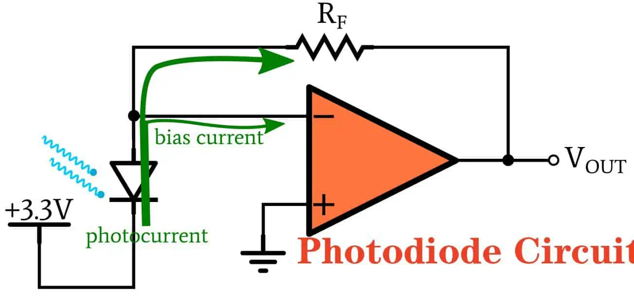
For starters, a photodiode is a little device that transforms light energy into current. These have mostly two corners called the P-side and N-side. You need to connect the P-side with a negative junction of the battery, and N-side goes with the positive one. 

So, if just a small amount of sunlight is put on a photodiode, it will change it into current in seconds. 

What is Photodiode Circuit?

A photodiode works similarly to a light detector that catches light and changes into current and voltage as per the use case. Now photodiodes are slow to respond in general cases when they are large.

It means the large surface area of a photodiode will not produce desired results

. You can also consider these similar to semiconductor diodes, but producing current and voltage from sunlight is the exception.ย 

Junctions of a Photodiode Circuit 

FULL PCB MANUFACTURING Quote

There are two types of junctions used by photodiodes, and these are:

  • PIN Junction
  • PN Junction


Components of a Photodiode Circuit 

There are different components of a photodiode. These include:

  • Lenses
  • Optical filters
  • Semiconductor

You must be thinking that a few types of photodiodes are the same as light-emitting diodes. Well, there are some similarities between the two that we need to discuss at this point. Both these diodes contain two junctions at the end. One is the cathode which is small, and the other is the anode which is large in size. 

  • Forward Bias: When the condition is forward bias, the current will be conventional, and its direction will be anode to cathode. 
  • Reverse Bias: Whereas when the condition is reverse bias, the current will go from cathode to anode. 

Types of Photodiode Circuit 

There is a large variety of photodiodes existing for the producers and users. These photodiodes vary in their features and purposes. Different types and different use cases. The functioning of these photodiodes is always the same; however, there are certain things that you must consider to get the appropriate photodiode for yourself. 

1. PN Photodiode Circuit 

  • It has been the first ever type of photodiode engineered and has vast applications in different domains.
  • Since it is an old type, you will not be stunned by its performance.
  • It performs its job mostly within its depletion area.
  • The size of the diode is really small compared to advanced diodes.
  • Also, it does not offer much sensitivity.

2. PIN Photodiode Circuit 

  • It is one of the typical photodiodes used nowadays.
  • Its role is to capture light and draw out photons from it. Also, this diode has no parallel for doing this job more efficiently.
  • The area between both the P and N terminals is large, which helps this diode trap more sunlight and get more photons out of it.
  • The capacitance of this diode is much smaller, which benefits its performance at the same time. 

3. Avalanche Photodiode Circuit 

  • Avalanche photodiodes are efficient for use when light is low.
  • The photon trapping ability of this photodiode is impressive, which is why it is exceptional in offering positive results.
  • However, one drawback of this photodiode is its noise which makes it less suitable for use in sensitive machines and other equipment.

4. Schottky Photodiode Circuit 

  • The junction of this diode is smaller in size, which reduces the capacitance at the same time.
  • Since the capacitance is less, it improves its performance at a fast speed.
  • Such a photodiode is crucial for improving the efficiency of optical communication, for example, fiber optics. 
  • It is beneficial when you need to work on higher bandwidth as well. 

How to choose the best Photodiode Circuit for yourself?

By far, it is clear that every photodiode has its own use cases and specifications. However, you don’t have to get confused between these since there are some factors that will help you for this purpose. Hereโ€™s how you can choose the best photodiode for your projects:

  • How much noise does the photodiode produce?
  • What is the wavelength of the photodiode?
  • Check about the reverse bias constraints of the photodiode you have your eyes on
  • What is the gain of the photodiode?
  • Is the photodiode responsive?
  • Does the photodiode support quantum efficiency?
  • What is the transit time of the photodiode?

Why do Photodiode circuits have extensive applications?

One reason can be their remarkable features. Due to this, several producers rely on different photodiodes to enhance the overall quality of their products. The devices that need to detect light mostly contain photodiodes. Letโ€™s take a look at the following reasons for the wide acceptance of photodiodes in different domains:

  • These offer impressive linearity as compared to incident light
  • The noise is low, which reduces the chances of failure
  • Wide spectral response for better performance
  • Mechanically rugged that enhances the efficiency 
  • Featherweight structure and small size for easy adjustment
  • More longevity, unlike other variants

How to make a Photodiode Circuit?

The discussion remains inadequate if we don’t teach you to make a photodiode with simple tips. Don’t worry; you don’t have to go above and beyond to make your first photodiode or maybe revise your style to make better ones. There is a list of important materials that you need to collect to combine them for a stunning and highly efficient photodiode! The list looks like this:

  • Silicon: The suitable electromagnetic spectrum wavelength ranges between (190-1100) nm
  • Germanium: Go for the wavelength that is between (400-1700) nm
  • Indium, Gallium, Arsenide: The recommended wavelength is (400-1700) nm
  • Lead II Sulfide: Use wavelength of <1000-3500 nm
  • Mercury, Cadmium, Telluride: A perfect wavelength ranges between (400-14000) nm


Which Photodiode circuits are lower in noise?

If we compare the abovementioned wavelengths of photodiodes, it is clear that Siliconโ€™s wavelength is suitable for producing less noise. 

Construction

Once you have all the important materials for the construction of a photodiode, it’s time to finally construct it. We are going to learn about the process in the following step-by-step guide:

  • You need two semiconductors (P-type and N-type) to produce a photodiode.
  • The P-type substrate is a little doped as compared to the N-type.
  • It enables seamless ion diffusion later.
  • The N-type substrate uses an epitaxial covering when constructing the photodiodes.
  • The purpose of this covering is to dope the N-type substrate more than the P-type.
  • Two contacts are important for developing the anode and cathode. 
  • You divide the diode among active and non-active regions for the sake of ease.
  • The non-active side is for Silicon Dioxide, while the active side is for trapping the sunlight.
  • The active side needs to be concealed with an anti-reflection substance that does not miss out on an iota of sunlight for transforming it into the current. 

Working on Photodiode Circuit 

Photodiodes follow a unique principle of working, and without discussing it, you will fail to understand the physics of photodiodes completely. So the function starts when the photodiode captures photons from sunlight. Now this will create electron holes on the photodiode because of the photoelectric effect. If absorption of these photons takes place in the depletion region, the electric field excludes the carriers present in this area. It will make the holes march toward the anode, and electrons will go toward the cathode. This movement will produce a photocurrent in the system. You need to keep the current as low as possible so that you can make the photodiode more sensitive for capturing sunlight.ย 

Modes of Operation of Photodiode Circuit 

There are three basic modes of operation among photodiodes. These include:

  • Photovoltaic Mode:  You can also call it zero-bias mode. There is a lightened photodiode that produces the voltage. It has a little dynamic range and does not need non-linear voltage at all. 
  • Photoconductive Mode: The type of photodiode required for this mode works on the reverse bias condition. The voltage is responsible for the improvement of the thickness of the depletion region. Due to this, the response time is less, along with the capacitance. Therefore, this is much faster than the photovoltaic mode. However, it makes a loud noise and might not be befitting for many applications. 
  • Avalanche Diode Mode: Avalanche diodes need high reverse bias conditions for work. The functioning of this mode looks like this. It amplifies the number of avalanches for all the electron holes. It results in more gain of the photodiode that gradually boosts the response. 

Advantages of Photodiode Circuit 

Wondering about the advantages of photodiodes? Well, these are not less! 

  • Photodiodes are efficient in offering less resistance when needed. 
  • These are reliable for fast speeds that are important for certain electronics.
  • These have more longevity.
  • The spectral response is also impressive of photodiodes.
  • Photodiodes do not consume much voltage.
  • These are durable, heavy-duty, and not heavy at all.
  • Photodiodes are highly sensitive to light which makes them efficient for several light-detecting devices.
  • Produce less dark current, which is important.
  • Offer impressive quantum frequency when needed.
  • Some types produce less mechanical noise, which is good.

Disadvantages of Photodiode Circuit 

Itโ€™s time to have an honest look at the drawbacks of photodiodes:

  • These are not reliable for temperature stabilization.
  • The current is not sufficient for operating the entire circuit at all.
  • The active area that traps sunlight is usually smaller in size.
  • Some types are poor, with light sensitivity.
  • An optimum temperature is important to make photodiodes work properly.
  • The photodiodes use offset voltage which can complicate different things.

Applications of Photodiode Circuit 

  • We are talking about some common applications of photodiodes first. These are photoconductors, photomultipliers, and photo-detecting devices.
  • Consumer electronics like CD players, TVs, smoke detectors, radios, clocks, camera light meters, and even streetlights use photodiodes.
  • Linear response photoconductors are crucial for the domain of science.
  • The medical field also relies on photodiodes, and medical equipment like monitors and tomography machines include photodiodes.
  • Optical communication also cannot breathe without such photodiodes for the sake of light regulation as well. 

An Ultimate Guide to Light Sensor Circuit: LDR Circuit

Light Sensor Circuit

In basic electronic projects, one of the coolest circuits is the light sensor circuit. Its main function is to detect the light in the surroundings, and the result can be detected by the brightness of the LED.

What does this circuit use for?? It is used for knowing the working of Light Dependant Resistors, Negative-Positive-Negative transistors, and the sensitivity of the resistor in the circuit. If we want to know the presence and absence of lights in the environment, these types of circuits can be used. These types of Light sensor circuits are used in commercial and non-commercial areas. These can be used in homes and industries. These can be used to save energy. If the street lights are on due to some negligence, then we can use these circuits to off them. These sensors can also detect X-rays.

It is a simple circuit that can control electrical appliances in homes and on the streets. We can control lights, fans, air coolers, street lights, and a number of other electrical appliances by using this circuit. To maintain load management, we can on and off these appliances by this circuit.

We can also control the street lights which are erected on risky highways. This circuit contains major electrical and electronic components

  1. Light sensors
  2. Darlington Pair
  3. Relay

Below is a brief introduction to these components.

ยท Light Sensor

Light Sensor Schematic

Different types of light sensors like photocells, photodiodes, PV cells, phototubes, PMT, phototransistor, and many more. But LDR is used as a light sensor in this light sensor circuit.

These circuits donโ€™t produce any kind of energy.

But the change in the light changes the resistance of LDR. It can be used in dirty environments. It can be used outdoors and indoors. We can say that this circuit is much preferable to another circuit with many qualities. Light intensity control Light DependentResistor (LDR). These resistors are composed of Calcium Sulfide (CAโ€™s), which is used to reveal photoconductivity. CAโ€™s is a high-resistance semiconductor material.

LDR exhibits a very high resistance of a few mega ohms during nighttime when the light illuminated on the LDR decreases. LDR exhibits very few resistances of 100ohms during day time when the light illuminated on the LDR increases. Hence the resistance decreases with the high intensity of the light illuminated on the LDR, and the resistance increases with the low intensity of the light illuminated on the LDR. We can say that the relation between resistance and the light is inversely proportional to each other.

ยท Darlington Pair:

Itโ€™s an electronic component made with the combination of two Bipolar Junction Transistors connected in such a way that it allows a very high amount of current gain. This transistor is used in this light sensor circuit. As compared to the general transistor, this Darlington transistor has a very high current gain.

The input delivered to the load through the Darlington pair is calculated as the sum of the transistor’s input current and gain. We are aware that if the base voltage is more than 0.7 volts, the transistor will turn on, but for a Darlington pair, two transistors must be turned on. Therefore, the base voltage must be 1.4 volts.

Relay:

In order to activate the load or to link the load to both the light sensor circuit and the AC mains, a relay is essential in the light sensor circuit.

The coil that typically makes up a relay is energized whenever it receives enough supply (the needed quantity of supply depends on the relay’s rating).

Practical Applications of Light Sensor Circuits:

FULL PCB MANUFACTURING Quote

The practical applications of Light Sensor Circuits are:

  1. It is used to design various embedded systems based on sensors such as security alarms and fire alarms etc.
  2. It controls street light systems automatically.
  3. It can manage a light system on a risky and dirty highway.

ยท Sunset to Sunrise Lightning Switch:

This switch is specially designed to control the light illuminated on the LDR light sensor automatically, as we know that the LDR resistance changes with the change in the light intensity illuminated on the LDR. The 555 timers are linked in biostable mode and receive the LDR output. The trigger of a load through a TRIAC is managed by the 555 timer’s output. As a result, this light sensor circuit automatically turns on the load at sunset in the evening and turns it off at sunrise in the morning.

ยท LDR Based on light Intensity Control for Street Lights

We use HID Lamps in a proposed system to turn on and off the street lights because the energy consumption of these lamps is high. But this HID Lamps system has some drawbacks, so in order to overcome these drawbacks; we use LDR because this system has LEDs to meet up the needs.

This project consumes low power as compared to HID Lamps because the light-depending resistor is installed in it, which reduces the light according to the daylight.

A streetlight is made up of a bunch of LEDs that can be controlled by this LDR system as the microcontroller has been installed in it, which is comprised of programmable instructions that control the light.

As traffic on the roadways tends to drop in the late hours of the night, the light intensity is kept high during peak hours. It then gradually declines till dawn. Finally, the street lights go out fully in the morning and come back on at 6 o’clock in the evening.

Everything You Need to Know About Proximity Sensor Circuit

You use different types of sensors throughout your day, and you might not even know them! It is uncanny how these superb inventions of physics have made our lives so much easier. Since the advancement of technology, these sensors are undergoing incredible upgrades to provide you with more feasibility and edge. There is a large variety of sensors that are now a crucial component of huge consumer electronics.

Be it your AC, baking oven, street lights, or coolers, these sensors are everywhere, making your devices perform at their finest! Today, we cannot even imagine our lives without these sensors since they have been serving us efficiently due to their remarkable features.

We have picked the proximity sensor circuit to discuss in this post. You are going to have a look at these sensors from a different perspective which is going to be fun! So letโ€™s hop onto it without any delay!

Systems of different Proximity Sensor Circuits

Before we jump onto the actual discussion, its time that we see what systems are appropriate for particular sensors to work:

  • PIR sensors (automatic door opening/closing system)
  • LDR sensors (automatic street lighting system)
  • Piezoelectric sensors (power generation system)
  • IR sensors (traffic signal system)
  • Ultrasonic sensors (obstacle detection system)

Proximity Sensor Circuit

proximity sensor circuit

A proximity sensor is a mechanism that is reliable for verifying the objects present near it that might touch it as well. Such a system works with electromagnetic radiation, and it can use electromagnetic fields in some cases. The electromagnetic field will change if the sensor detects any object lying around it. Now when we talk about proximity sensors, we will call this object the target of the sensor. There are different types of targets that you can place around a proximity sensor. These can be of plastic or metals. As per these targets, we get different types of proximity sensors which lead us to our next section!

We will go in-depth about these types of proximity sensors later in the next sections for you!ย 

Features of Simple Proximity Sensor Circuit

  • These are highly precise in the results.
  • This offer a short response time.
  • These have more longevity.
  • These work on non-contact detection phenomenon.

Principle of Proximity Sensor Circuit

  • As you know, the purpose of a proximity sensor is to detect the objects around it within the nominal range. The sensor will not detect non-metallic objects at all. 
  • There is a magnetic coil that generates the electromagnetic field for the sensor when the power supply energizes the coil.
  • After this, when an external disturbance influences this electromagnetic field, it will cause it to produce an eddy current that will cover the disturbance. The disturbance, in this case, is our target which will interfere with this electromagnetic field. It will also cause the load to reduce the intensity of the electromagnetic field. 
  • Now here is what happens: When you will bring the target closer to the sensor, it will boost the eddy current, which will cause the load to amplify the vibrations as well. It will reduce the strength of the electromagnetic field ultimately.
  • There is a trigger that will detect these vibrations based on the distance of the target and will turn the switch ON/OFF as per the condition.
  • The opposite will happen, and the vibrations will boost when you take the target away from the sensor.  

Major Types of Proximity Sensor Circuits

FULL PCB MANUFACTURING Quote

1. Inductive Proximity Sensor Circuit

These sensors do not need contact for their performance. 

  • Inductive proximity sensors use inductive law for object detection.
  • The distance of the metallic object determines the oscillations produced by the coil.
  • You can find this sensor in two variants in the market. One is the shielded version, and the other is the unshielded version. 

2. Unshielded Proximity Sensor Circuit

  • There is no disturbance in the electromagnetic field of the coil which means it will allow a higher range of detection. 
  • The oscillator, Schmitt trigger, coil, and output switch circuit make up an unshielded version of an inductive proximity sensor. 
  • When the coil gets energized due to current, it will produce an electromagnetic field. 
    When the sensor detects a metallic object, the eddy currents will cause changes in the inductance. 
    After this, the current will also change the final output on the whole. It happens with the sensorโ€™s switch, which is responsible for monitoring. 
  • In the absence of a target, the sensor will keep vibrating, while in the presence of the target, it will cause the sensorโ€™s switch to trigger. 
  • The use cases of this circuit are mostly in commercial areas where land mining and metal detection are important applications. 

3. Capacitive Proximity Sensor Circuit

  • These are also non-contact sensors and can detect metallic and non-metallic objects. It means these are multipurpose, unlike inductive proximity sensors.
  • When this sensor detects any peculiar shifts in the capacitance, it will notify or beep. 
  • It has the same components as the inductive proximity sensors.
  • However, there are two capacitor plates in this sensor, from which one is present inside the sensor, and the other is outside. 
  • You connect the internal plate with an oscillator, while the external plate will pair up with the detecting region of the sensor. 
  • An electrostatic field is important to make this system work. 
    When it comes closer to a target, the capacitance will increase, and it will also boost the oscillatorโ€™s gain. 
  • Applications like touch devices and moisture controllers often use capacitive proximity sensors. 
  • Ultrasonic Proximity Sensor Circuit
  • Such a sensor is useful for applications like automation and production.
    It will detect its target based on the nominal range or, in simple words, distance. 
    These sensors work on a frequency of 20 kilo-hertz, which is higher than the audible frequency range of humans.
  • It does its job by generating an ultrasonic signal and receiving them back.
    After this, it will determine the time disparity between the outgoing and incoming ultrasonic signals, which helps it to find out the distance of the target. 
    Just a transmitter and a receiver will make this circuit up. You can palace them together or separate them for individual units.

5. Optical Proximity Sensor Circuit

  • These are among the most affordable types of proximity sensors that you would ever know.
    You can trust them for automated applications, and they are easily adjustable within congested areas.
  • There is a light source for this sensor which will enable it to detect light. 
    Now there is also a light sensor which is basically a semiconductor that is reliable for producing light for once only. 
  • These sensors have important applications in copy machines, light fixtures, and alarm systems. 

6. Magnetic Proximity Sensor Circuit

  • It works by detecting the magnetic field around it, which means it can only detect the presence of a magnetic object.
  • When the object interacts with the sensor, it will trigger the sensor causing it to turn ON. 
    These are also non-contact sensors and work more efficiently than the other versions of proximity sensors. 
  • There are many principles of physics that a magnetic proximity sensor works on. These are reed switches, GMR inductive, and magnetoresistive. 
  • Major Applications of Proximity Sensor Circuit
  • We have grouped some of the fascinating applications of proximity sensors for you!
    Whenever you need to detect a metallic object, you can use a proximity sensor for this purpose.
    It not only detects the presence of an object, but it also determines the distance within the nominal range.
  • Smartphones also use proximity sensors.
  • Smart home appliances and home automation devices completely rely on proximity sensors.
  • Different industrial-grade tools and rolling mills also use proximity sensors.
  • The conveyor belts used in the factories and at the airports use such sensors to count all the items moving on them.
  • Tracking systems, distance measurement devices, electrical motors, and speed determination also work with proximity sensors.
  • You can use photoelectric proximity sensors for the purpose of detecting the presence of plastic objects.
  • Inductive proximity sensors are for detecting metallic objects, and the ultrasonic version will identify the target based on this distance. 
  • Some proximity sensors will detect both metallic and non-metallic objects.

Disadvantages of Proximity Sensor Circuit

Irrespective of the fact that proximity sensors have remarkable features and have significant applications in different domains. There are some considerable drawbacks of these sensors that you should know. There have been cases when complications occurred for the projects since the users were unaware of these drawbacks of proximity sensors. So make sure you are choosing the right variant of a proximity sensor for yourself!

  • Temperature and humidity can influence the performance of proximity sensors.
  • Their designs are complex, and there is no margin of negligence when it comes to their construction.
    The range through which they can detect the objects is variable as per the sensorโ€™s type
    Some types are expensive to produce as well.
  • The inductive sensors are less accurate than other types of the proximity sensors.
  • Technical glitches in the proximity sensors can ruin the entire device.

How to Measure PCB Hole Size

Measure PCB Hole Size

During the production of electronic devices, some holes have to be drilled. Some years ago, PCB designers drilled simple holes to make their boards. Then, the circuit boards were moved onto the usual position and a lever began the drilling. After this, the same board would be moved to the next position for a repetition of this process.

As time went by, the circuit board became smaller and the manufacturing process became more complex. Therefore, this made the traditional drilling process impossible. These days, there are now standard drill sizes for circuit boards which make the drilling process much easier and even faster.

What are PCB Hole Sizes?

The printed circuit boards produced today are smaller in size and have more than 10,000 holes in different sizes. Although the automated CNC tools allow PCB manufacturers to drill any hope size without extra effort, this process is simpler with the standard drill sizes.

During the production of blank circuit board, there are some things you need to keep in mind. These are the purpose and the maintainability of the final PCB. Some circuit boards donโ€™t have the necessary thickness to withstand every drill bit. So, it is recommended to ensure the hole size is less than your PCB aspect ratio.

You donโ€™t just determine the hole size of your board, some factors do. A good example of such is the Vias. The sizes and shapes of Vias will usually vary and some things determine this. The complexity of a circuit determines the shape or size to use.

0.006 inches hole size is very small. For such holes, PCB manufacturers will need laser drills. However, the majority of builds will need “micro Vias.” Also, multiple size drills are usually a must if multiple board layers are involved.

Holes are usually drilled on every circuit board. These holes connect the board to the ground plane. This is because it is impossible to solder the hardware on the board. Sometimes, the PCB manufacturer adds some Vias to offer perfect ground connections. Also, these holes offer support to the circuit board when they are exposed to excess torque when the nut is being tightened.

How to Calculate PCB Hole Size

A VIA hole in a PCB

It is very easy to calculate the PCB hole size. All you need to do is to follow the necessary steps:

First, find the maximum diameter of the components. This determines the types and shapes of holes that needs to be drilled. You can use round holes if the PTH lead is round while the square shape is ideal for square PTH lead.

You can calculate the minimum size by determining the maximum Lead Diameter which could be +0.25mm or 0.20mm.

The next step is to determine the size of the annular ring. For level A, the size of the annular ring should be 0.05mm while 0.5mm should be for level B. Then 0.4mm for level C. This indicates that the pad diameter should be the sum of  the minimum home size,  minimum fabrication allowance, and minimum annular ring.

Calculating PCB Hole Diameter

The aspect ratio of a board determines the PCB determines the calculation of a PCB hole diameter. For instance, if the board thickness is 1.60mm, and the size of the hole is 0.49, the aspect ratio will be 1:4. When you reduce your board thickness, there should be a reduction in the aspect ratio.

The hole size diameter for a non-plated through hole differs from a plated through hole. For instance, when calculating for a non plated through-hole, you add the finished hole size and 0 mil.

On the other hand, calculating the hole size diameter for a plated through hole requires adding 0.10mm or 4 mil and the finished hole size.

What are the Standard PCB Hole Sizes?

There are various drill and hole sizes provided by the PCB industry. PCB manufacturers charge differently for hole sizes. While some PCB manufacturers charge for each drill size, some provide standard PCB hole sizes.

The PCB hole size chart provides PCB standard hole size in inches. A good number of PCB manufacturers offer their standard PCB hole sizes. The standard hole size can be calculated by subtracting the standard thickness of through-hole metal plating from standard drill bit sizes.

Furthermore, the printed circuit board must meet the specifications of the size state in the design drawing. This means the PCB must adhere to specifications like openings, cutouts, thickness, slots, and perimeter.  The bonding must be within ยฑ0.01millimeter and the error of the wire width must be within ยฑ5%.

The engineer handling the drill press will be forced to use the next larger drill bit or choose the next smaller drill bit if there are no standard sizes. Also, the engineer may consider the PCB as non manufacturable.

PCB designers approximate the non-standard PCB hole sizes closer to the larger standard hole size. For instance, the holes drilled for DIP packages are usually approximated to 0.9mm diameter.

There are different standard PCB hole sizes. But, it is important to adhere to a simple rule in order to choose the best PCB hole size. Ensure your holes are 0.3mm wider than the component in order to get the best fit. For instance, if your component is 0.4mm, the hole size will be 0.7mm.

According to the SSS specifications, only 500 holes should be created on a circuit board . However, the DSS specifies that the maximum number of holes on a PCB should be 2000.

Importance of the PCB Hole Size Chart

FULL PCB MANUFACTURING Quote

One of the vital things that help you determine the hole size of a board is the PCB hole size chart. It is simply a description of the general information of holes. With this chart, a PCB designer will be certain of where to place components. In quite a number of cases, creating the holes via which components are placed can be a very complex process.

Due to this, PCB manufacturers must specify the dimensions and tolerance of the holes. In this case,  the PCB hole size chart plays a huge role. A PCB hole size chart specifies important details about the hole size.  Such information helps you plate the circuit board in the right way.

How to Get the Perfect PCB Drill Size

If you want to achieve the perfect drill size for your circuit board, look into these guidelines.

Know the lead diameter

You need to be sure of the lead diameter of thick components on your board. Also, you need to determine the maximum lead diameters from the datasheets.

Calculate the Minimum Hole Size

You can calculate the minimum hole size once you know the maximum lead. You will get the minimum hole size by adding 0.25mm to maximum lead diameter. i.e Minimum Hole Size = Maximum Lead Diameter + 0.25mm.

Calculate the pad diameter

The minimum hole size will help you get the value of the pad diameter. When calculating, use the smallest pad area. Most times, the value is always about 50 micrometers it 0.05mm. Furthermore, it is advisable to add a fabrication allowance when calculating the pad diameter.

Know the difference between the density level

There are different level of ย component densities. These are level ย A, B, and C. ย Level A is highly preferred among the PCB manufacturers. This is because it offers benefits such as low component density and high footprint geometries. ย On the other hand, the default standard for the majority of PCB projects is Level B. This level is commonly known for solid solder attachments. The last level which is C features a high design productivity standard.

How to Calculate PCB Through Hole Size

Measure PCB Hole
Measure PCB Hole

You need to take account of the right size of the plated through-hole and its pad when creating a through-hole PCB footprint. Using the right dimensions will prevent any issue from occuring during the PCB assembly. If the hole size is very small, this component pins can’t go into the hole. Therefore, the PCB layout has to be redone.

If there is a small distance between the pin’s edge and the hole’s wall, there won’t be a smooth flow of  solder from one side of the board to the other. If otherwise, the solder will fill the hole. In these two cases, the components won’t solder firmly due to insufficient solder.

Also, if there is a small pad diameter is too small, there could be poor soldering connection.

There are four steps you need to follow to achieve accurate through hole size:

  • Be certain of the performance classes and density of PCB design
  • Find the lead diameter
  • Know  the size of the plated through-hole
  • Get the pad diameter

Conclusion

PCB hole specifies the best location to place the through holes or copper pads. When fabricating a board, holes are usually drilled. In most cases, PCB holes are usually not plated through. It is important to note that any hole drilled in a circuit board needs to be carefully measured. Therefore, it is crucial to drill holes perfectly. PCB holes enable a board to achieve proper functioning.

Thermal Via in PCB 101: Design Guidelines, Types, and Best Practices for Heat Dissipation

Active components can serve as significant heat sources in your PCB, directly influencing the board’s equilibrium temperature. Repeated thermal cycling (high-to-low transitions) and prolonged high-temperature operation degrade system longevity, often leading to premature component or trace failures. Implementing an effective thermal management strategy is critical to mitigating these risks.

A key element of this strategy is the strategic placement of thermal vias. These vias enhance heat dissipation away from high-power components such as processors, FPGAs, and power electronics. By optimizing thermal via placement in your PCB layout, you can reduce peak temperatures, eliminate hot spots, and significantly improve system reliability.

What Are Thermal Vias?

Thermal pad PCB
Thermal pad PCB

Thermal vias are specialized through-hole connections in a PCB designed primarily for heat transfer. Unlike standard vias used for electrical connections between layers, thermal vias are strategically placed to conduct heat away from components and distribute it more effectively across the board or to dedicated heat sinking layers.

Key Characteristics of Thermal Vias:

  • Typically smaller in diameter than standard vias
  • Often clustered in arrays beneath heat-generating components
  • May be filled with thermally conductive materials
  • Can span multiple layers of the PCB

Read more about:

How Thermal Vias Dissipate Heat

Understanding the mechanism behind heat dissipation through thermal vias is crucial for effective implementation. Thermal vias work on the principle of conduction, one of the three primary heat transfer methods (along with convection and radiation).

The Heat Dissipation Process:

  1. Heat Generation: Electronic components, such as power transistors or high-speed processors, generate heat during operation.
  2. Conduction to PCB: This heat is initially conducted to the PCB surface directly beneath the component.
  3. Thermal Via Network: An array of thermal vias beneath the component provides multiple pathways for heat to travel.
  4. Vertical Heat Transfer: Heat moves vertically through the vias, utilizing the high thermal conductivity of copper.
  5. Layer-to-Layer Spread: As heat travels through the vias, it spreads laterally at each layer, increasing the effective heat dissipation area.
  6. Heat Sinking: In many designs, thermal vias connect to internal ground planes or dedicated heat sinking layers, further enhancing heat distribution.
  7. External Dissipation: Finally, heat is dissipated to the environment through the PCB surfaces or additional heat sinking structures.

Types of Thermal Vias in PCBs

Thermal vias come in various configurations, each with its own set of advantages and use cases. Understanding these types can help designers choose the most appropriate solution for their specific thermal management needs.

1. Standard Thermal Vias

Standard thermal vias are the most basic and common type. They are essentially normal plated through-holes used for thermal purposes.

Characteristics:

  • Unfilled
  • Typically 0.3mm to 0.5mm in diameter
  • Used in arrays for increased thermal conductivity

Advantages:

  • Cost-effective
  • Easy to manufacture
  • Suitable for moderate heat dissipation needs

Disadvantages:

  • Less efficient than filled vias
  • Can trap air, reducing thermal performance

2. Via-in-Pad

Via-in-pad technology integrates thermal vias directly into the component’s solder pad, allowing for more efficient heat transfer and space-saving designs.

Characteristics:

  • Vias placed within the component’s footprint
  • Often used with BGAs and other dense packages

Advantages:

  • Improved thermal performance
  • Reduced PCB real estate usage
  • Shorter electrical paths

Disadvantages:

  • More complex manufacturing process
  • Risk of solder wicking during assembly

3. Filled and Capped Vias

Filled and capped vias represent the most advanced thermal via technology, offering superior heat dissipation capabilities.

Characteristics:

  • Vias filled with thermally conductive material (e.g., copper, silver, or thermal epoxy)
  • Capped with copper for a smooth surface

Advantages:

  • Excellent thermal conductivity
  • Prevents solder wicking
  • Allows for component placement over vias

Disadvantages:

  • Higher manufacturing costs
  • Requires specialized production processes

4. Micro Vias

Micro vias are extremely small thermal vias, typically used in high-density interconnect (HDI) boards.

Characteristics:

  • Diameter less than 0.15mm
  • Often laser-drilled
  • Can be stacked or staggered

Advantages:

  • Enables very high via density
  • Suitable for fine-pitch components
  • Improved signal integrity

Disadvantages:

  • More expensive to manufacture
  • May have limited depth due to aspect ratio constraints

How to Maximize the Effectiveness of Thermal Vias

To achieve optimal heat dissipation using thermal vias, designers must consider various factors and implement best practices. Here are key strategies to maximize the effectiveness of thermal vias:

1. Optimize Via Placement

  • Place vias as close to the heat source as possible
  • Use arrays of vias rather than single, larger vias
  • Consider the direction of heat flow when placing vias

2. Choose Appropriate Via Size and Spacing

  • Balance via diameter with manufacturing capabilities
  • Space vias close enough for effective heat spread, but not so close as to compromise board integrity

3. Utilize Multiple Layers

  • Connect thermal vias to internal ground planes and power planes
  • Use dedicated thermal layers in multi-layer designs

4. Consider Thermal Via Filling

  • For high-power applications, use filled vias for improved thermal conductivity
  • Choose filling materials based on thermal requirements and budget constraints

5. Implement Proper PCB Stackup

  • Place high-conductivity layers closer to heat-generating components
  • Use thicker copper layers for improved heat spreading

6. Combine with Other Cooling Techniques

  • Integrate thermal vias with heat sinks or cooling fans
  • Use thermal vias in conjunction with thermally conductive PCB materials

6 Benefits of Using Thermal Vias in Your PCBs

Incorporating thermal vias into PCB designs offers numerous advantages:

  1. Enhanced Heat Dissipation: Thermal vias significantly improve the board’s ability to remove heat from components.
  2. Improved Component Reliability: By reducing operating temperatures, thermal vias can extend the lifespan of electronic components.
  3. Space Efficiency: Thermal vias allow for more compact designs by reducing the need for large heat sinks or spacing between components.
  4. Flexibility in Component Placement: Effective heat management through thermal vias enables more freedom in component placement on the PCB.
  5. Cost-Effective Thermal Management: Compared to other cooling solutions, thermal vias are relatively inexpensive to implement.
  6. Compatibility with High-Density Designs: Thermal vias are crucial for managing heat in densely packed, high-performance PCBs.

Combining Thermal Vias with Other Thermal Management Strategies

A heatsink on a graphics chip

While thermal vias are highly effective, they are often most powerful when used in conjunction with other thermal management techniques. Here are some complementary strategies:

1. Heat Sinks

  • Attach heat sinks to components or PCB surfaces
  • Use thermal vias to enhance heat transfer to the heat sink

2. Thermal Interface Materials (TIMs)

  • Apply TIMs between heat-generating components and the PCB
  • Use in combination with thermal vias for improved heat conduction

3. Forced-Air Cooling

  • Implement fans or blowers for active cooling
  • Design thermal via patterns to work with airflow patterns

4. Liquid Cooling

  • For extreme thermal requirements, consider liquid cooling solutions
  • Use thermal vias to efficiently transfer heat to liquid cooling channels

5. Thermally Conductive PCB Materials

  • Select base materials with higher thermal conductivity
  • Combine with thermal vias for optimal heat spreading

6. Power Plane Design

  • Optimize power and ground plane design for heat distribution
  • Connect thermal vias to these planes for enhanced thermal performance

16 Thermal Via Design Tips for Efficient Heat Management

  1. Conduct Thermal Simulations: Use thermal modeling software to optimize via placement and size.
  2. Consider Manufacturability: Design thermal via patterns that are feasible to produce with available technology.
  3. Use Larger Diameter Vias for High-Power Components: Increase via size for components with higher heat output.
  4. Implement Redundancy: Design with extra thermal vias to account for potential manufacturing defects.
  5. Balance Thermal and Electrical Requirements: Ensure thermal via placement doesn’t compromise signal integrity.
  6. Adhere to IPC Standards: Follow industry guidelines, such as IPC-2221, for thermal via design.
  7. Optimize Via Aspect Ratio: Maintain appropriate depth-to-diameter ratios for effective plating and heat transfer.
  8. Consider Thermal Expansion: Account for differences in thermal expansion between PCB materials and components.
  9. Use Thermal Relief Patterns: Implement thermal relief connections to balance heat dissipation and solderability.
  10. Avoid Voids in Filled Vias: Ensure proper filling techniques to prevent air pockets that reduce thermal efficiency.
  11. Implement Teardrop Connections: Use teardrop patterns to strengthen via connections and improve heat spread.
  12. Design for Even Heat Distribution: Spread thermal vias evenly to avoid hot spots on the PCB.
  13. Consider Top and Bottom Layer Heat Dissipation: Utilize both sides of the PCB for maximum thermal performance.
  14. Optimize Copper Weight: Use heavier copper weights on layers connected to thermal vias for better heat spreading.
  15. Implement Thermal Fences: Create barriers of thermal vias to isolate heat-sensitive components.
  16. Document Thermal Design Intent: Clearly communicate thermal via requirements in PCB design files and documentation.

Thermal Vias Simulation and PCB Examples

To illustrate the effectiveness of thermal vias, let’s explore some simulation results and real-world PCB examples.

Thermal Simulation Example

A thermal simulation of a high-power LED module demonstrates the impact of thermal vias:

  • Without Thermal Vias: Peak temperature of 85ยฐC at the LED junction
  • With Thermal Vias: Peak temperature reduced to 65ยฐC
  • Result: 23.5% reduction in peak temperature, significantly improving LED lifespan and performance

PCB Design Example: Power Supply Board

In a 4-layer power supply PCB design:

  • Thermal Challenge: High-power MOSFETs generating significant heat
  • Solution: Array of 20 thermal vias (0.3mm diameter) under each MOSFET
  • Implementation: Vias connected to internal ground plane and bottom-layer copper pour
  • Outcome: 30% reduction in MOSFET operating temperature, enabling higher power output

High-Frequency RF Board Example

For a high-frequency RF amplifier board:

  • Thermal Challenge: Maintaining low temperatures while preserving signal integrity
  • Solution: Micro vias (0.1mm diameter) in via-in-pad configuration
  • Implementation: Stacked micro vias connecting to buried heat-spreading layer
  • Outcome: Achieved required thermal performance without compromising RF characteristics

Conclusion: The Critical Role of Thermal Vias in Modern PCB Design

As electronic devices continue to shrink in size while increasing in power and complexity, effective thermal management becomes ever more crucial. Thermal vias represent a powerful, flexible, and cost-effective solution for addressing these challenges in PCB design.

By understanding the principles behind thermal vias, their various types, and best practices for implementation, PCB designers can create more efficient, reliable, and high-performing electronic products. Whether you’re working on a simple consumer device or a complex industrial system, integrating thermal vias into your PCB design strategy can lead to significant improvements in thermal performance and overall product quality.

As technology evolves, we can expect to see further innovations in thermal via design and implementation. Staying informed about these developments and continuing to refine thermal management techniques will be essential for PCB designers aiming to push the boundaries of electronic design and meet the demands of future technologies.

Remember, effective thermal management is not just about preventing failureโ€”it’s about optimizing performance, extending product lifespan, and enabling the next generation of electronic innovations. Thermal vias are a key tool in achieving these goals, and mastering their use is a valuable skill for any PCB designer in today’s fast-paced technological landscape.

What is PCB Trace Impedance Calculator in Electronics Industry?

impedance control pcb

Mathematics and science follow a simple rule of precision and accuracy. They mainly give accurate measurements of events, actions, and items. It still leaves a person thinking; therefore, it needs key consideration while designing, manufacturing, and analyzing the physical structure. The uncertainty principle of Heisenberg is found in most mathematical, scientific, and engineering projects. However, this principle states that the speed and position of an item cannot be measured at the same time. Therefore, scientists and engineers are still looking for solutions to measure them altogether.

Determining an ideal value of impedance plays a vital role in designing a PCB, especially a high-speed PCB design. This gives the definition of trace parameter control and the choice of board material. Exclusively calculating and analyzing the impedance of a PCB brings various challenges. However, the impedance control significance of a board makes it necessary to use a reliable and durable method to give efficient results. Thus, letโ€™s dive into some available options and find a solution for calculating the impedance control of a PCB, which gives practical and accurate results.

Methods of PCB Trace Impedance Calculator

YouTube video

Propagation of signals in the layout of PCB occurs in the transmission line. But this task seems quite challenging. The circuits of today comprise compact, multifunctional, and complex designs. This literally implies that a PCB has to encounter various types of signals like DC, RF, and digital, distinct trace types like stripline and microstrip with variant orientation and size. However, there are some considerations to follow, which include clearance and creeping, edges of the board, design of footprint pad, and spacing and width of the trace. Moreover, there may add up more concerns like matching the impedance of output and input connections and the type of material that may affect the impedance. 

Thus, managing these considerations may end up in unmanageable situations. Besides these parameters, it may also include the goals of signal integrity maximization, removing reflection, and reducing the EMI or noise. Other than managing these parameters, the impedance control of PCB still comes first and needs serious interest and a determined approach. To make calculations simple, it’s important to deduct pre-hypothesis. This is associated with each design’s uniqueness which implies that it gives various possibilities for measuring the impedance control of the board. Eventually, the result you will get in the end may vary to a certain aspect because of different techniques. Anyhow, the methods described below are fully practical and applicable.

Methods for Calculation 

ยท Smith Chart

A Smith chart is one of the oldest methods. It came into being ages before PCB layout software and computers were developed. Its main purpose is to determine the relation of the reflection coefficient between load and source impedance. It then uses a mathematical manipulation series to get the value of impedance for a trace or line. 

ยท Computer Simulation

The advanced design software of PCB packages contains a feature of impedance control calculation. It gives benefits: you can access the available design parameter and can modify it automatically to perform different simulations. This way, you can choose an ideal design for PCB manufacturing. However, the only drawback of such type tools makes the software much more expensive. 

ยท Online Calculator

Online calculators prove an ideal than software with design packages of PCB for control impedance. As online calculators offer features to calculate impedance control or parameters of trace with desired impedance. Although it does not act as completely as simulation software, these may place you under the ballpark, which needs a little but necessary tweaking from your manufacturer for the PCB manufacturability. Most online calculators follow the principle of the Design Guide of standard IPC-2141A for Controlled Impedance of PCB with High-Speed.

How Does PCB Trace Impedance Calculator Works?

Core-built PCBs impedance control

Each trace possesses a small, almost unnoticeable series of inductance spread alongside the trace, which has a proportional relationship with a trace cross-sectional area. The impedance becomes noticeable as the time of rise increases. In the same manner, each trace also has capacitance alongside the return signal path and the trace. This serves as a function of trace width and material of dielectric between the trace and the return path of the signal. Here again, if the time of rise increases, the generated impedance becomes significant as the electrical current flies across this capacitance.

The drivers interpret traces in the form of transferred LC circuits and the AC impedance of the trace generated from this dispersed LC circuit. This refers to uncontrolled impedance. However, manufacturers do not try to design the environment for the trace for this very impedance. This allows the capacitance and the inductance to change along with the trace, as this impedance does not usually affect the operations, so you donโ€™t have to spend any money or time designing methods to manage it.

ยท Controlled Impedance

However, a question arises: what if the impedance affects the operations? In this situation, design a circuit where traces resemble the transmission lines. This allows us to terminate the trace capability of impedance to bypass the reflections. 

While controlling impedance, ensure that the trace has constant impedance at each end rather than changing from time to time, just like in a standard uncontrolled impedance case. Impedance control requires three parts of the geometry of the circuit to control. This includes trace width, the coefficient of dielectric of the substance around the trace, and the value of spacing between the trace signal and the return path signal. For instance, the coaxial cable serves as a transmission line with impedance control.

You can also alter these geometric aspects and get controlled impedance only as far as you keep altering other aspects as necessary. So that the relation between these features does not modify and the value of impedance stays constant.ย 

How To Confine Trace Impedance with PCB Trace Impedance Calculator?

PCB Impedance

The process of manufacturing circuit boards with controlled impedance must have the ability to calculate the impedance. The impedance trace calculator of PCBs helps in calculating the trace impedance. You can access these calculators in the CAD software or online. There are various factors to consider while calculating the impedances. This includes trace thickness, trace width, laminate thickness, copper weight, and dielectric thickness. 

Once you get the values of all the parameters, adjust them to a certain level to calculate the impedance. Once you reach a desirable level of impedance, test the effectiveness of the board through test coupons. These coupons are built altogether in the same plane. This way, you get an appropriate value of impedance without facing any trouble while accessing actual board traces. It gives an accurate value if the traces of the test coupon and the traces of the boards are similar.

Generally, the fabricator creates the test coupons over the edges of the manufacturing panel so that you can get the authentic value of impedance through these test coupons without defecting the circuit. 

The trace impedance can also be calculated through a network analyzer, TDR, or test system of controlled impedance with TDR techniques. A specialized and skilled engineer uses test systems of impedance to measure the impedance, which ensures high-end results. 

How Does Design and Layout Affect Trace Impedance?

In an actual PCB design, signal impedance can be quite distinct from the ideal desired value from the design schematic. This occurs because of the substrate’s presence and trace arrangement on the circuit. This increases some significant effects, such as crosstalk. This alters the value of impedance from the desired value. PCB may experience problems of power integrity, like ringing when a PCB shifts high frequencies. The power-delivered net impedance also turns from the desired capacitance behaviors of PCBs at higher frequencies. This takes part in the integrity of power and potential signal problems. 

ยท Transmission Line Impedance

The transmission line impedance is categorized through the values of impedances. Characteristics impedance plays one of the essential. This simply refers to the transmission line impedance of PCBs in complete isolation from other transmission lines. The value typically equals 50 ohms. Though, it takes distinct types of values based on the standard of signaling in a device. For instance, LVDS mainly features that the impedance differential of distinct parts must equal 85 Ohms.

Some other metrics that define the impedance of transmission lines mainly depend on the alignment of two distinct transmission lines. Because of the capacitance of parasitic effect which arises due to circuit substrate material and the shared inductance between 2 close transmission lines. Transmission lines are also categorized with odd and even values of impedance. Differential and common impedance is linked with other values, which brings the complete value of impedance that defines the transmission line up to five.

ยท Power Delivery Network Impedance

The network of power delivery may show the impedance capacitive at a very low frequency, which decreases power bus resistance in the series along with the return path of ground and load components at DC. The physical spacing between the traces, internal planes, and power planes in the circuit dominates this impedance. However, as the frequency of driving increases, the mutual inductance inside the circuit enhances the power delivery systemโ€™s impedance. Ultimately, the power delivery net impedance may exhibit various peaks at a high frequency

Ideally, the power delivery net impedance must be flat inside the band that you will work with. The bandwidth depicts all the frequencies between a knee frequency and a clock rate for digital. Moreover, if the harmonics that contain digital signals read a similar frequency, then a function of transfer for the return signals in the ground layer must be flat. Therefore, the same approach applies to the analog signals which travel throughout the ground planes and the board.

Whereas the spectrum of impedance becomes essential for determining the bandwidth that possesses minimum impedance of power delivery. The spatial impedance distribution in the ground planes plays a more important role, especially in devices with mixed signals. Signals pass through the path which has the least reactance on the return ground when passing through ground planes. Furthermore, the least reactance path in multipoint topology, point-to-point, and a star must lie under the conductors of the circuit. This ensures that the circuit must have a minimum inductance of the loop and have less EMI susceptibility.ย 

ยท PCB Substrate Material Selection

FULL PCB MANUFACTURING Quote

Because of the parasitic interference, you have to select the PCB substrate material carefully and design the stack-up. The substrate material has a dielectric constant which affects the design geometry to create transmission lines alongside specific impedance. This directly affects the net power delivery impedance. The conductors inside the planes also define the impedance of the loop in a PCB, which directly affects the EMI susceptibility of the circuit. 

ยท Impedance Matching Networks

The PCB stack-up affects various features of the design circuit. This includes routing strategy and thermal resistance. PCB design with appropriate substrate material can help in reducing the risk of loss of signals while managing the constant impedance across the circuit. The maintenance of PCB impedance to a certain value during the process of routing is essential. It ensures the matching of impedance throughout the net. Once the signals transfer to a transmission line mode, make sure that the drive, receiver, and transition line must have a constant impedance to avoid the reflections of signals.

Conclusion

Impedance control refers to a method of regulating PCB trace strength by calculating its impedance. The control of impedance has become the standard practice of PCB because of the frequently altering frequencies of high-tech devices and applications. 

Impedance control can be measured by utilizing the test coupons after the manufacturing of the PCB. Test coupons serve as a PCB which gauges the efficiency of the manufacturing process of PCBs. However, test coupons also make on the same line as a PCB, typically on the edges. After the production process, test coupons go through an evaluation process that checks the alignment of layers, internal structure, and electrical connectivity. You can choose coupons from the collection of suppliers or specially created for the PCBs. PCB manufacturers can also design test coupons or can place them on functional panels.

The Essential Guide to Voltage Sensor Circuit: Types & Working Principle

Voltage Sensor Circuit

What would you say if someone asked you to define the general purpose of a sensor? Well, a sensorโ€™s job is to detect an electrical signal and behave according to that signal. Now, the significance of sensors is unbelievable for the efficient performance of the electronics. In fact, some sensors even protect the devices from undergoing potential damage and failure.

These sensors are more feasible to use because of their small sizes, weight, and guarantee of safety at the same time. You can use a single sensor to determine current and voltage if the nature of your project is like this. However, we are going to take a look at voltage sensors and the major aspects of these circuits in detail. 

What is a Voltage Sensor Circuit?

The voltage sensor is not a simple circuit to describe. However, we are going to make its definition a lot more perceivable for you so that even if you don’t belong to a physics background, you can understand a voltage circuit quite well. Here we go:

We define a voltage sensor as a setup that is responsible for monitoring the voltage surge and voltage drops. These circuits show accurate readings and voltage traces. Since electronics need precise amounts of voltage to work efficiently, now you know a voltage sensor is a huge deal for such machines.

Some voltage sensors produce pulse waveforms and sine waveforms as well. Now if your project needs a different output, you need some standard voltage dividers to find this output accurately.ย 

Working Principle of Voltage Sensor Circuit

Voltage Sensor Circuit schematic

For AC voltage: 

When you are working with AC voltage, there are some considerations that you should keep in mind. Don’t worry if you do not know them yet; we are going to discuss these with you for the sake of the quality of your upcoming projects:

  • If your voltage sensor uses an AC voltage, then a transformer is important that should consist of sensing elements to make your setup work.
  • Other than a transformer, when you want, you should reduce the voltage level to low, which will cause the AC voltage to change into DC voltage. It means you can switch the nature of voltage from AC to DC and vice versa. 

For DC voltage: 

As you know the considerations of the AC voltage, its time to learn about what you are going to do when you are working with DC voltage in a voltage sensor:

  • In this case, a transformer is useless; instead, you need an A/D converter which is an important part of a complex voltage sensor.
  • Apart from an A/D converter, you need a resistor that consists of a sensing element that will pair up with the DC voltage.
  • However, remember to use more voltage than the sensing elements; otherwise, this setup won’t perform as per your expectations.
  • Also, power regulation and control are necessary when you are observing DC voltage. 

Characteristics of Voltage Sensor Circuit

It will be just redundant to say that voltage sensors have crucial applications for the well-being of giant industries around us. Isnโ€™t it so obvious to you?? Due to this reason, consumer electronics is no exception. Every type of voltage sensor has a different set of features that make it different from the others. Nevermind, we are going to take a quick look at the general characteristics of voltage sensors for you:

  • Excellent wireless nature so that you can connect it with as many external equipment and devices as you want.
  • These are able to proactively monitor voltage drops and voltage spikes for the real-time detection of technical problems.
  • Microcontrollers also work well with voltage sensors so that the devices can efficiently perform in their natural state. 
  • Voltage sensors are always accessible from the market, and producers can fully rely on them.
  • These are affordable to use for private projects, which helps students with their assignments as well. 

Different Types of Voltage Sensor Circuits

The following are two major and common types of voltage sensors:

Resistive Type Voltage Sensor Circuits

  • The resistive sensors include two circuits normally. One of them is a voltage divider circuit, and the other is a bridge circuit.ย 
  • This circuit also contains a resistor, and it has the simple job of functioning as a sensing element for this circuit. 
  • The voltage gets divided into both circuit units of this sensor equally. 
  • When the circuit receives the voltage supply, it allows you to find out the output voltage, and resistance helps you with this purpose.
  • Unlike the voltage divider circuit, the bridge circuit has a group of four resistors. 

Capacitor Type Voltage Sensor Circuits

  • There is a single insulator and two conductors present in this sensor.
  • These three components are present in the core of the circuit. 
  • You need an appropriate supply for this sensor to get the desired results. 
  • The applied voltage will repel the electrons, which will create a detectable difference. 
  • If you use a series circuit, you can combine the voltage and capacitance for this type of voltage sensor. 

Benefits of Voltage Sensor Circuitย 

FULL PCB MANUFACTURING Quote

The following benefits will convince you to replace typical measuring techniques with voltage sensors to make your projects stand out from your competitors:

  • Small size
  • Featherweight
  • More safety guaranteed
  • Hight accurate results
  • Non-saturable nature
  • Eco-friendly
  • Multipurpose circuit for voltage and current

Applications of Voltage Sensor Circuit

  • It is reliable for the purpose of Load sensing in various devices.
  • Fault identification with a voltage sensor becomes easy, and you can even save your devices from undergoing irreversible damage.
  • Power loss detection makes electronics power-efficient, and all this happens due to a voltage sensor.
  • Temperature control and regulation with a voltage sensor seem unusual, but it has a great impact on a deviceโ€™s overall health.
  • Power demand monitoring is also a fantastic use case for a voltage sensor.
  • A voltage sensor never compromises on safety which becomes more important than ever for the well-being of devices so that they can perform naturally in the long run. 

Frequently Asked Questions (FAQs):

What is the meaning of a Voltage Sensor Circuit?

Voltage sensors are important for monitoring and determining the voltage supply of the electronics. You can find out the AC/DC voltage levels as well. It uses voltage as input and switches as its output. 

What are the various kinds of Voltage Sensor circuits?

Following are the different types of sensors available in the market:

What is the working of the Voltage Sensor Circuit in Arduino?

It acts as a voltage divider in Arduino. Moreover, it works on the ratio of resistance 5:1. It has two resistors of 30kilo-ohms and 7.5kilo-ohms. Besides, It reduces the output voltage to factor 5, no matter the input voltage. 

What are the two elements of a Voltage Sensor Circuit?

There are two major parts within a voltage sensor. One is the voltage divider circuit, and the other is the bridge circuit. These two parts play their individual roles in making the sensor perform its role efficiently for the devices, even under unfavorable conditions. 

Exploring the Benefits of Frequency Counter Circuit Working and Applications

Frequency Counter Circuit

The counter is widely used in digital devices to count the number of signals or any other event. It stores information and creates flip-flop groups using clock signals. Counters help in measuring the time and frequency as well as commence the counting operation. This enhances the memory location based on the application and device.

Counters have two basic types. Asynchronous counter and synchronous counters. Moreover, the โ€˜Mod’ refers to the modulus counter, which determines the number of states that needs to apply before calculating the signals. Frequency counters are widely used in digital clocks, timer circuits, frequency dividers, and ana-to-digital converters. 

This article gives you a detailed insight into how a frequency counter works, its types, advantages, features, and applications. So letโ€™s dive into it. 

What Is a Frequency Counter Circuit?

Frequency counters refer to a type of device that integrates various types of radio frequency devices to measure the time and frequency of digital input signals.

They have the ability to measure the time and frequency of repeated input digital signals precisely and accurately. Moreover, the frequency counter also refers to a frequency meter as it calculates the time and frequency of input pulses and square wave signals.

RF range devices also use this. They simply use Prescaler, which minimizes the frequency of the signal and helps a digital circuit to operate. Moreover, it shows the frequency of analog or digital signals over the display screen in Hz.

The counter starts counting the pulses when the number of pulses occurs in a given interval of time. It transfers them to a frequency counter device. This, however, shows the frequency pulse range and sets the counter to zero. It has a digital display which makes it easy to use and operate. Moreover, it gives accurate results at affordable prices.

Block Diagram Explanation of Frequency Counter Circuit

Frequency Counter schematic

The block diagram of frequency contains threshold, input conditioning, input signal, AND gate, display, flip-flop, decade dividers, latch or counter, and accurate clock or time base.

1. Input

When a counter receives input signals with high-impedance input and low-impedance output, it sends it to an amplifier which converts the input signals into a rectangular wave or square wave for operating in a digital circuit. Thresholds and input conditions are utilized in amplifying and buffering input signals. Moreover, it uses Schmitt triggers to manage the additional counting pulses that occur because of the noise and disruption at the sides. Therefore, controlling the counter sensitivity and trigger level can minimize the counting of extra pulses. 

2. Clock

An accurate timebase or clock helps in creating various timing pulses at specified time intervals. Moreover, it uses high-quality crystal oscillators for accurate and controlled timing signals. This cloak is then applied over the decade divider. 

3. Decade Dividers & Flip Flop

The input and clock signals produce pulses that go through a decade divider. It divides the timing signals. The received output then goes through a flip-flop. It creates a precise enabling pulse to go to the AND gate.

4. Gate

The accurate enabling pulse from the flip-flop and input signal series then goes through the AND gate. Here it creates a pulse series at an accurate time interval. If the input signal has a 1 Mhz frequency and passes through the open gate just for 1 second, it creates 1 million output signal pulses.

5. Counter & Latch

The output from the gate then goes to the counter. It computes the number of pulses obtained from input signals. However, the latch holds the signals of output while the counter calculates the pulses and displays the figures over the display. The latch goes through 10 stages of counting and holding the pulses.

6. Display

The display shows the output signals received from the latch and the counter and displays them in an understandable format. It shows the signal frequency. It uses display screens like LED or LCD. As every decade counter has one digit, it displays the rest of the information over the display.

Circuit Diagram Explanation of Frequency Counter Circuit

The diagram of the frequency counter includes a counter, two timers, a potential resistor, an 8051 microcontroller, a generator of square waves, and a display (LCD).ย 

It uses an integrated circuit 1555 timer. It produces clock signals in one second of the specified time interval. Arduino UNO acts as a generator of square waves. Both the IC 555 counter and generator of a square wave refer to an astable multivibrator. Other than that, it uses an LCD of 16×2 inches which shows output signal frequency in Hz. 

It uses an 8051 microcontroller counter and IC 555 timer. The integrated circuit 555 timer produces oscillating signals using a 99% duty cycle and gives output signals with the highest interval period. The discharge resistor and threshold adjust in a way to get the required duty cycle value. It uses the duty cycle formula of

D = (R1+R2)/(R1+2R2)

The 8051 microcontroller counter generates the pulse frequency in Hz. As 8051 contains two timers, of which one acts as 0 timers and one-timer. At the same time, they operate in 0 modes and one mode. Timer 0 helps in producing a delay in time while timer 1 counts the number of pulses coming from the generator of the square wave.

 Operating Principle of Frequency Counter Circuit

FULL PCB MANUFACTURING Quote

The generator of square waves produces a pulse that goes through the 8051 counter. It uses two modes of operation, delay the time and pulse counting. The 8051 counter calculates the input signal number of pulses at a given time interval. The output received from the counter then displays to an LCD of 16×2 which shows signal frequency in Hz. This is how a frequency counter works. 

Major Types Of Frequency Counter Circuit

Frequency counters have two types that help in measuring the signal frequency. These types include Direct counting and Reciprocal. 

ยท Direct Counting 

This approach serves as the simplest and most common method to measure input signal frequency. First, it counts the input signal cycle every second. Then a common counter circuit is used to measure the frequency. This, however, does not give appropriate results and has limitations in measuring low-frequency resolution. It expands the time of the gate to measure the high resolution. For instance, to measure a high resolution of 1 MHz, then it needs a 1000 seconds interval to measure a one-time signal.

ยท Reciprocal Counter

This approach overcomes the drawback of the first direct counting approach. It calculates the input signal period rather than measuring the input signal cycles every second. It uses the formula F = 1/T to calculate the pulse frequency. However, the final resolution of frequency depends on input frequency independence and temporal resolution.

It has the ability to measure low frequencies at high resolution quickly. Moreover, it adjusts the trigger phrases and minimizes the noise. It measures input signal time and manages to maintain enough time resolution. Additionally, it does not cost much. 

Other than these two frequency counters also have other types. This includes a panel meter, a frequency counter with a digital multimeter, and a handheld frequency counter. Additionally, a bench frequency counter which is used in electronic test devices, and a PXI frequency counter. It is used in control and test systems and shows frequency in the formality of PXI.ย 

Advantages of Frequency Counter Circuit

Frequency counters offer various benefits and features. The measurement of square wave generating signal frequency happens in accurate time intervals. Moreover, frequency counters are vastly used in frequency measurement in the radio-frequency range.

It does not only give accurate results but also gives easy and quick. However, based on the usage and application, it costs less. Also, it makes sure that all frequencies must transmit within a band. 

Applications of Frequency Counter Circuit

A frequency counter is used in a variety of applications and devices. Firstly it is used to measure the square wave generating signal frequency. It also measures the signal frequency from an oscillator.

It does not only measure the frequency but gives an accurate measurement. Moreover, it measures input signal frequency over the receiver and transmission line. Due to clock signals, it uses data transmission. Moreover, it only works in the range of RF. In addition, it can also measure high power transmission data frequency.

Frequently Asked Questions 

What is the unit or symbol of word frequency?

Hertz or Hz is used as the unit of signal frequency.

What is the major benefit of a Frequency Counter Circuit?

A frequency counter is used to analyze accurate signal frequency produced from an oscillator or a square wave producer.

Which type of Frequency Counter Circuit is best to measure frequency with high values?

The high-frequency measurement uses an asynchronous and synchronous counter.

What is the meaning of Mod Counter?

Modulus counter refers to a Mod counter that uses clock signals to count a number of times a counter counts pulses sequence. 

What Are The Two Main Techniques Of Frequency Counter Circuit?

Frequency counters use Reciprocal and Direct counting methods. 

Conclusion

Frequency counters refer to a very sensitive device whose accuracy depends on the timebase precision. However, the timebase may vary according to age, instability, poor design, and movement. Therefore, make sure to give extra care to the timebase while working with frequency counter projects.

How to Use Desoldering Wire

Desoldering Wire

Soldering can be described as a reliable way for joining copper pipes during plumbing works as well as for assembling electrical components inside a printed circuit board. This creates reliable and strong joints.

However, what will happen when you solder a wrong pipe or component? What if the soldered pipe or component has no use and you want it to serve a different purpose? This is simple; all you need to do is to take out the component by desoldering this solder joint or melting the solder. Whenever you are Desoldering, you must choose the appropriate tool and method for removing these components. By this, re-using the components will be possible.

Otherwise, these components will become damaged during the whole process and using them again will be impossible.

YouTube video

What are Desoldering Wires?

How to Use Desoldering Wire

A desoldering wire, which is also called desolder wick, is made up of copper threads which are braided together. Normally, flux is added to aid the flowing of the solder from the jumper, where it isnโ€™t meant to be, into the wick. Therefore solder wick is at times referred to as desolder braid. You can solder virtually everything, and the desoldering wire forms a huge part of the entire process.

This method of soldering wick is useful for taking out any unwanted solder after the soldering process. The making of the soldering wick is made through the intertwining and braiding together of the copper coils. Therefore, it is termed desoldering braid.

Furthermore, soldering wick is manufactured using copper wires because they are great heat conductors. As this solder gets attracted to heat, these copper coils suck the solder up from the surface of the metal.

There are soldering wicks that come with flux. This allows solder to be removed from its surface. Also, when the solder wick doesnโ€™t have a flux, you may dip the wickโ€™s end part into some of the flux so as to enhance the solder removal speed. Three types of desoldering wires are possible to serve different uses. These include:

  • No-clean: These are low-residue halogen-free flux coated braids that are spooled on the ESD safe ribbons.
  • Unfluxed: The copper braid left untreated and spooled on the ESD safe ribbons
  • Regular: This is the rosin flux having treated copper braids

Things to Do To Desolder

Below are some of the things you must do to desolder

  • Intertwine few inches of the copper wire and then create a braid
  • Then apply some of the flux on this copper braid through the dipping of the end in flux
  • Place some of this solder wick on those joints you wish to desolder
  • Keep the hot soldering iron at the solder wickโ€™s tick as well as the desired pin
  • Wait for some seconds till this solder melts and the melted solder is sucked by the solder wick
  • Take this solder wick and then take that part of the wick, which has been covered using solder
  • Then, repeat this process until this unwanted solder has been removed.

When handling this solder wick, make sure that it isnโ€™t touched with your bands because of its extreme hotness. Just use some pliers to hold as well as position it.

What are the Safety Tips to Take Note of During Desoldering?

FULL PCB MANUFACTURING Quote

Similar to soldering, there are some safety precautions that you must adhere to strictly during desoldering. If you fail to do this, you could have serious injuries.

Work with these safety tips in order to have a safe a great desoldering experience

  • User well-ventilated areas during desoldering
  • Avoid touching the element or tip of the soldering iron
  • After use, ensure the soldering iron is placed on its stand
  • When handling the components, use pliers during desoldering
  • The solder must not be touched with your hands
  • Make use of gloves, masks, and safety glasses
  • Donโ€™t put on loose-fitting clothes
  • Have a fire extinguisher and first aid kit ready

When Should a Desoldering Wire be Used?

While the desoldering pump or solder sucker functions like the vacuum cleaner, the desoldering wick functions more like mops. The ability of the latter for absorbing solder ensures it is very useful in applications whereby solder splatter cannot be accepted.

This makes this desoldering wick better when cleaning off solder from the SMT pads as well as removing the solder bridge found on the BGA pads and fine-pitch SMT which are usually seen on modern PCBs that have been populated with the SMD components. Though the best way to desolder the SMD components are by making use of the hot air rework stations as well as special desoldering tweezers the desoldering wire or wick is also utilized for this task.

Also, the desoldering pump is clearly useless for all SMD reworks. This is due to the fact that the PCBโ€™s conductive pads are just too flat to allow the sucking out of the solder effectively. It is similar to drinking of soup from your dinner plate using a straw.

Removing Solder Using Desoldering Wire

Using the desoldering wire wrongly might tear patters from the PCB as well as damage some discrete components. To prevent problems like these, ensure these [preventive measures highlighted below are taken.

  • Apply flux to whatever joints you want to desolder
  • Place your desoldering wire on the joints and place this soldering wire on a wire
  • This soldering iron will melt the solder. This is pulled in the desoldering wire. Immediately this solder has been taken out, lift this wire and then iron the board off.

Tips for Proper Removal

Though using it seems easy, utilizing wrong techniques might lead to thermal damages to the printed circuit board and its components. Extending the soldering iron contact to the component or board might lead to thermal damage. Also, if this desoldering wick doesnโ€™t remove the solder, try the steps highlighted below.

  • Apply a little solder onto the joint
  • Also, apply some solder to the soldering iron tip
  • Apply little quantity of solder at the desoldering wire tip. This aids easy removal
  • Cut the wireโ€™s soldered tip at a 45 degree angle. This ensures that solder present at its tip isnโ€™t cut off

When you apply some solder to the joint, the tip of the desoldering wire, this helps to cut surface tension as well as permit the easy absorption of the jointโ€™s solder by the wires.

During the process of desoldering, if you need to cut the desoldering wire, cut it at an angle of 45 degrees with the solder still present, this also helps in trimming the wire whenever it is saturated with the solder and will not be able to absorb again.

Choosing the Right Desoldering Wire and Tip

electronic assembly soldering

Below are some things to consider when choosing the right desoldering wire and tip

Braid Width

You can find desoldering wick in different widths starting from 0.8 mm and can go above 5 mm. A general rule says that the width of the braid must be slightly larger or equal to the size of the pad. Braids that are smaller wonโ€™t wick off solder from the whole pad, whereas the oversized ones would affect the nearby pads that you didnโ€™t plan to solder

Size of Soldering Tip

This same logic is applicable to the tip of the soldering iron. It has to match the width of the braid. When it is too small, the heating becomes slower. This causes the dwell time as well as the risk of damages to the components. Also, the oversized tips may knock the neighboring components off.

Flux Composition

Finally, the composition of the flux utilized for the desoldering wick is important as well. If the workflow is relying on no-clean solder due to the fact that you want to do skip cleaning, then you have to make use of a desoldering wick which has no-clean flux infused with it. Also, if you want to clean the post rework of your PCB assembly, desoldering wick that has been imbued with a rosin flux ill have the fastest wicking action.

Advantages and Disadvantages of Desoldering Wire

Advantages

  • Simple, cheap, and easy method
  • Great method for taking out solder from the flat surfaces
  • Desoldered components can be reused
  • Supplied on pre-cut or spool strands
  • Soldering wick comes in different sizes; this depends on the quantity of solder that you wish to remove
  • The soldering wickโ€™s size can be modified. This depends on the quantity of solder that you wish to remove

Disadvantages

  • The soldering wick cannot be reused. The portion that is covered in solder must be cut
  • As this soldering wick become very hot, positioning it against its joint could be difficult
  • With this method, removing solder out of pinholes could be difficult

Conclusion

In summary, the process of desoldering is utilized in melting the solder as well as removing the materials that have been soldered. By making use of the right methods and tools, you can take out the components without causing any damage and then reuse them.

What is Electromechanical Assembly in Printed Circuit Board Assembly?

pcb assembly jobs

Electromechanical methods of assembling PCBs refer to the combined efforts of using electronic and mechanical processes for the circuit boardsโ€™ operations. This article highlights the basics of electromechanical assembly, the different variants you can choose from and some of the benefits.

What is Electromechanical Parts Assembly?

It refers to the process of using mechanical and electronic components, as well as subassemblies to manufacture an electronic device. The need for this process is buoyed by the need to make electronic devices fully electronic.

At the core of electromechanical assembly process is the creation of a definitive unit and the creation of a seamless integration of the productโ€™s mechanical and electronic aspects.

Here are some quick facts about the electromechanical assembly manufacturing process:

  • It allows for the creation of a fully-functional system โ€“ one that connects the electronic components to the mechanical elements.
  • The assembly process also leads to the creation of a system that utilizes electronic current for performing mechanical operations.

Electromechanical Components List

SMT-assembly-board

The list of components used for the electromechanical assembly often alternate between the mechanical and electronic elements. However, it is also possible to use other components, such as subassemblies.

Mechanical Components

The following are some of the mechanical elements used in electromechanical assembly:

  • Casings
  • Motors and;
  • Gears

Electronic Components

The following is a list of some of the electronic components used for electromechanical assembly:

  • Sensors
  • Printed Circuit Boards (PCBs)

The list of electromechanical components also includes the following:

  • Programmable Logic Controllers (PLCs)
  • DIN Rails
  • Power switches
  • Power supplies
  • Cable and wire assemblies
  • Enclosures
  • Electric motors and;
  • Varieties of circuitries.

Categories of Components Used in Electromechanical Assemblies

You may have thought that the assembly process uses just the combined components from both electronics and mechanics. However, there are three (3) broad categories of these parts, as discussed below:

Mechanical Components

The function of these parts is to account for the visible (physical) attributes of the electronic device. Parts like fasteners, motors, enclosures and gears are used for this purpose.

Electronic Parts

These components are used to build the electrical functionality of the electronic devices. The likes of capacitors, Integrated Circuits (ICs), Printed Circuit Boards (PCBs) and resistors are used here.

Electromechanical Parts

These are the combined components functioning both as electronics and mechanics. Connectors, switches, and solenoids are examples of the parts that have properties of both mechanical and electrical devices.

Types of Electromechanical Assembly Services

The complexity of the device and the targeted applications are some important considerations for the electromechanical assembly types.

These are some of the common ways to assemble electronic devices:

1. Cable and Harness Assemblies

This process refers to the use of wires or cables meant for transmitting electrical signals within the device.

Some of the cable and harness parts are:

  • Ties: these are used to affix the wire harness to the device.
  • Wires and Cables: these are designed to convey the signals and electrical current within the device.
  • Insulators: these components protect the electronic devicesโ€™ components from touching the environment and from touching each other.
  • Fuses: these are in place to regulate electrical current, and in extension, reduces the risks of power-induced damages to the device.
  • Connectors: these are used to connect the wires and cables in the electronic device.
  • Relays: the function of the relays is to turn on and off the power in the high-amperage circuits.

2. Mounting Rails

Also called the DIN Rails, these are used to mount several other components within the electromechanical assembly.

3. Motor Assemblies

These are the types of electromechanical assembly used for ensuring movement within the electronic device.

4. Switch and Sensor Assemblies

Also called the control panels, they help in bolstering the interactions and controls of the electronic device.

They are broadly categorized into:

Sensor Assemblies

These refer to the parts used for converting light, sound, motion and heat into the corresponding electrical signals.

Examples of the components used for the sensor assemblies are:

  • Connection Heads: these parts enable the sensor wiresโ€™ connection to the transmitter.
  • Sensing Elements: these components are used for detecting proximity and the physical properties, such as radiation and temperature.
  • Transmitters: these are used to transfer the data (pieces of information) obtained about the targeted property.
  • Housings:ย these are used to protect the sensor-related components.

Switch Assemblies

These components are primarily used for connecting or disconnecting the power supply to the electrical components.

Examples of the switch assembly components are:

  • The Switching Mechanism: this is a pushbutton used for controlling the electronic deviceโ€™s operations.
  • Contacts: these parts allow for the flow of electric current to the deviceโ€™s switch.
  • Wiring Harness: the harness provides the pathway for the entry and exit of electric current from the switch. It is also used for holding the electric switch in position.

5.ย Power Supply Assemblies

FULL PCB MANUFACTURING Quote

These are the components used for the conversion and distribution of electrical current within the electronic device. These parts include:

  • Regulators:ย these are used for reducing the filterโ€™s ripple voltages.
  • Transformers: these components are used for modifying the voltage coming into the system.
  • Filters: are used for smoothing out the waves in the Direct Current (DC) output. This happens after the rectification process.
  • Rectifiers: used to convert the incoming voltage from Alternating Current (AC) to Direct Current (DC).

6. Box Builds and Integrations

This infers to the process of building full systems of electromechanical assembly called box builds. We can also handle the integrations for you, such as integrating a circuit board into full harnesses, enclosures and a front panel assembly equipped with switches and connectors.

7. Panel Assemblies

This type of electromechanical contract manufacturing requires the integration of the components into panels. The aim of the integration is to streamline the process of distributing power into the connected circuits.

The panel assembly process includes wiring the panel, positioning the components in the back panel and drilling the holes for mounting the hardware.

8. Transformer Assemblies

The process of transformer assemblies involves aiding the transfer of electrical current between multiple circuits.

The process includes the insulation of materials, lamination of the core, making primary and secondary windings.

The Benefits of Electromechanical Assemblies

Despite the complexities, using the electromechanical process of assembling electronic devices comes with some perks, such as:

Device Modernization

Electromechanical assemblies support the reevaluation and upgrade of the existing electronic devices.

Specialized Services

You can get specialized electromechanical assembly services from the Contract Manufacturer (CM). With the longstanding years of experience and the use of specialized equipment, the electromechanical assembly technician has the know-how to optimize the complexity of the electronic devices.

Prototyping

The support for prototyping and testing allows for the early-stage validation of the electromechanical assembly products.

Affordable Electronic Product Manufacturing

You also get to save up on extra costs when using the electromechanical assembly. Thanks to the box build and integration process, you can reduce the overall production costs.

The electromechanical contract manufacturing company will be handling most aspects of the product, such as:

  • Component sourcing
  • Handling the facility, labor and equipment costs.
  • The manufacturerโ€™s access to a set of established supply chain networks also helps you to save costs on logistics.

How to Choose Electromechanical Contract Manufacturing Companies

pcba box build assembly

Want to work with a Contract Manufacturer (CM) for your electronic device production? Here are some of the tips on choosing the best company:

Quality Assurance

The products or electrical devices should meet the minimum quality standards. Therefore, the company should have the relevant facilities and certifications to offer electromechanical assembly services.

Check the Technical Capabilities

This refers to the Contract Manufacturer (CM)โ€™s ability to handle your electronic device project, as per your requirements.

The manufacturer needs the know-how and pieces of equipment to make this work.

Volume of Orders

Does the electromechanical assembly CM have what it takes to produce the volumes (numbers) of electronic devices you want?

First, find out if the company supports micro electromechanical assembly, which means that it allows for the production of a few products.

The manufacturer should also be able to handle large-volume orders.

Track Record

This refers to the Contract Manufacturer (CM)โ€™s many years of experience. It also refers to the different projects it has been able to process, thanks to the extensive years of experience.

The reason for this consideration is that an experienced CM is the one that can easily detect and fix issues, as well as produce your devices, as per the requirements.

Box Build Electromechanical Assemblies

Does the company offer box build solutions? If it does, it makes sense, as it saves you time and money. The specifications of the box build solutions include sourcing the components and managing the entire electromechanical assembly in-house.

How to Get Started with Electromechanical Assembly

Haven satisfied yourself that using electromechanical assembly can improve your electronic projects, start by contacting a professional manufacturer. We will help you make custom-built solutions that match your projectsโ€™ preferences, serve the needs of the target market and save you costs.

You can be sure of getting your electronic devicesโ€™ electromechanical assembly solutions handled in-house by our experienced engineers and all these will be completed in the shortest lead time possible.