What is the Importance of Optical PCB?

Optical PCB

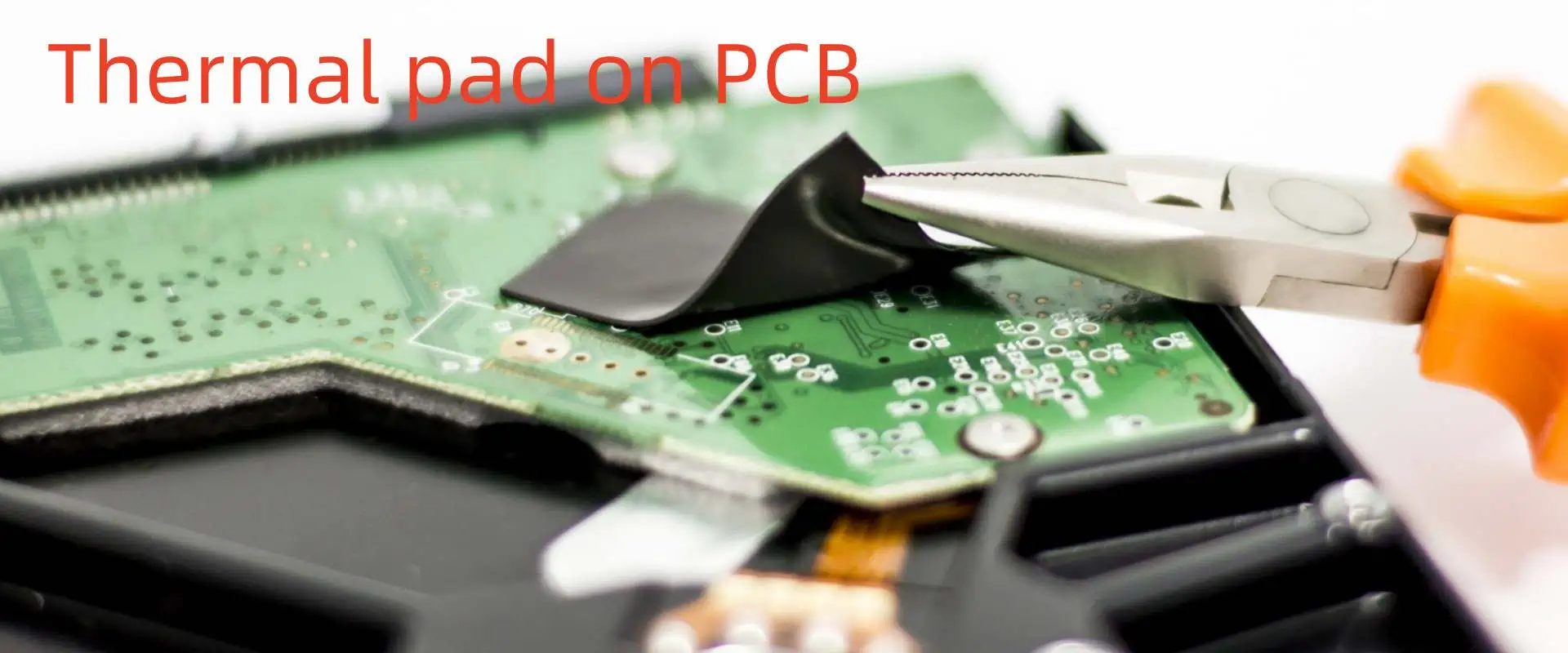
The interconnection required to boosting the performance of Internet switches is directly proportional to the final outcome of data aggregation. As the next-generation Internet switches emerge, we need a reliable interconnection to make them work. That is what you will get by using optical PCB.

In this article, we define what an optical circuit board is, the relevance in the market and some of the benefits.

What is an Optical Printed Circuit Board?

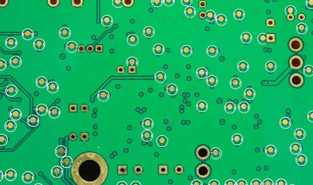
It is a type of circuit board used to produce dedicated interconnects, required for the connection of optical interconnects.

Optical Interconnects on a PCB?

You may be wondering why these interconnections are brought to the PCB-level. Given the ever-increasing use cases and or applications of Printed Circuit Boards (PCBs), it is not entirely surprising that optical interconnections are made here.

At the core is the need to leverage fiber optics, as a means to an โ€œendโ€ โ€“ towards forging an integration of optical interconnects onto Printed Circuit Boards (PCBs).

This is a step away from the conventional use of chip-to-chip interconnects, which, though have been in use for some decades, is now giving way to newer technologies.

Today, we can now commercialize optical interconnects, on the basis of Photonic Integrated Circuits (PICs).

Although todayโ€™s optical PCB is still based on a construction out of COTS components, we are optimistic of what the future holds.

Market Opportunity: Why Optical PCBs Became Popular

Automated-Optical-Inspection

The primary goal for producing optical circuits is to streamline the speed of processing data rates.

Other reasons include:

1.    The Need to Prevent Signal Loss Issues

The current Internet switches are not fully-equipped to handle the data rates. With the expectations of higher data rates from the next-generation Internet switches and high-end computers, it has become imperative to step-up on the performance of these switches.

However, the current switches are processing data packets (rates) in Gigabytes per second (Gbit/s). This is lower than the anticipated Terabytes per second (Tbit/s) data rates of next-generation Internet switches.

If the current switches and interconnection technologies are relied for this, one can be sure of signal loss, in the process of transmitting data rates.

2.    The Wire Geometry Consideration

This is another important consideration. The geometry of the wire makes it nearly impossible to leverage the existing electrical interconnection technology. For example, we currently have more of copper wiring that inhibits data transmission rates in the following ways:

  • The inverse proportion of the wireโ€™s length to the cross-sectional area, and the proportion of the resistance to the wireโ€™s length.
  • The wire is usually thinner, and this further reduces the data transmission rates.

3.    Limitations in Scaling

There is currently a challenge in scaling or extending the performances of electrical/optical interconnects. This is because of several factors, such as:

  • Reflection
  • Signal loss
  • Crosstalk
  • Space constraints that donโ€™t allow for thicker wire usage
  • An increase in noise and power consumption, due to the use of a harder connection to reduce conversion time.
  • An increase in power consumption and operational costs for scaling current interconnects, up to 100 Gb/s.

How Optical Interconnects are Integrated into PCBs

Optical interconnects are currently constructed from the COTS components, but there are indications that, in the future, we will have these interconnects directly printed on the circuitsโ€™ substrates.

It is also worth noting that the integration of optical waveguides in the PCBs also aid the integration of optical interconnects. With the potentials, these would greatly improve the overall performances of the onboard interconnects.

The Advantages of Optical PCB

Besides reducing the link length for the high-speed electrical signals, the integration of optical interconnects into PCBs also offer these benefits:

a.    Independent Propagation of Signals

Signal loss and integrity problems are the common challenges with conventional electrical interconnection technology. This is now been tackled with the fusion of optical interconnects into PCBs.

The optical signals can now make independent propagations, devoid of the restrictions in space. This is also enhanced by the use of an imaging processing technology that delivers good dimensional integrity of the waveguide layer.

b.    Improved Speed and Overall Performance

The overall performance of the optical circuit board is assured, because of these reasons:

  • The optical interconnectionโ€™s speed is separated from the interconnection channel.
  • A photo-imaginable waveguide material is used to help meet the processing and functional requirements.

c.    Improved Reliability

With the optical PCB technology, one can be certain of deriving improved reliability of the signals, courtesy of these reasons:

  • Optical signals can propagate in three-dimensional (3D) free space.
  • There is a considerable increase in the data transmission rate.

d.    Balancing Performance and Cost

It is now possible to have both an improved performance at affordable costs, with the new optical PCB framework.

In addition to reducing the physical size of the electrical connection, it also aids the reduction of power consumed, while cutting down on the cost of the material used.

Typical Applications for Optical PCB

Cavity PCB board
Cavity PCB board

With the inputs of the optical circuit boards, we can now see that the use cases for these boards are further expanding. Now, you can use these boards to enhance the different applications and communications.

The following are some examples of the typical applications:

  • Opto-micromachine
  • Telecommunications and;
  • Photonic interconnection

Besides the above, optical circuit boards have also been used in other places. Most importantly, the photonics and optical interconnects jointly enable the usage in advanced applications, such as:

  • Future Telecommunication Networks: these are used to reduce the numbers of electronic components in both base stations and edge servers used for future telecommunication networks, such as 5G.
  • Quantum Computing: photonics is used here to ease cryogenic requirements, as well as serving as an alternative to superconductors commonly used in quantum computing.
  • AI Applications: the applications and or devices powered by or leveraging Artificial Intelligence (AI) also benefit from optical circuit boards. In this case, both Integrated Circuits (ICs) and optical interconnects are used to facilitate a higher and speedier data transfer between the systems and different components in a datacenter.

Design Constraints for Optical PCBs

Although we are adopting optical circuit boards into modern consumer electronics and related products, there are still some gaps that need to be filled.

Here are some of the constraints or challenges facing the massive adoption of optical PCBs:

a.    Immature Technology

The first challenge is the inability to further the advancement of the technology required for building the optical circuit boards.

In the past, heavy reliance was placed on the use of material and processing technology for the fabrication of waveguides. With the recent developments, more efforts need to be in place for โ€œmature manufacturing technologyโ€ to be used, especially for the production of optical circuit boards in their numbers (mass productions).

b.    The Materialโ€™s Platform Needs to be Considered

One important consideration is the choice of the material platform to be used. As a rule of thumb, the platform needs to be scalable, as well as enabling the fabrication of interconnects, in-between the photonic circuits.

c.    The Choice of I/O Interfaces

The Inputs and Outputs (I/Os) interfaces are also worth considering. In this case, we are looking at the intersection or interface where the chip meets the circuit board.

d.    Reliability of the Final Product

There is a need to be certain of the reliability of the final product. This is important, considering that the waveguide layer, after being fabricated, would need to be laminated to a conventional electrical layer.

Therefore, the adhesion or reliability of the final product is a major concern, seeing that the material configuration of the two layers differ.

Thus, it is important to have a balanced view and process to the method, considering that the waveguide material would be subject to degradation, provided the lamination is higher.

e.    The Need to have a Functional Photo-Imaginable Material

There is also a need to have the photo-imaginable material developed to match both the processing and functional requirements. This is because the material is used to make-up the cladding layer and waveguide core.

Here are the different requirements:

  • The cladding layer should be compatible with traditional circuit board materials. An example is Flame Retardant 4 (FR-4). By so doing, the cladding material will provide excellent adhesion between the electrical and optical layers.
  • On the other hand, the waveguide core material should meet the basic functional requirements, such as optical loss. The core materials should also match the processing requirement, an example being viscosity.

f.     Good Dimensional Integrity

As a must, the waveguide core layer must be in a good dimensional integrity, especially after the development. A coating method that provides excellent thickness distribution across the circuit board is commonly used for this purpose.

Conclusion

In conclusion, you can use optical circuit boards can be used as a means to further the transfer of data across different electronic components and devices. In addition, you can further niche-down the use of these circuit boards, as per the applications.

For example, there is the fiber optic circuit board used to conduct or transfer large amounts of data at faster speeds, and with additional safeguards.

On the other hand, there is the oscilloscope PCB, which is a device dedicated to measuring different parameters of electric signals. By this provision, the device for these purposes:

  • Monitoring the operation of the electronic equipment.
  • Checking the circuit board and its componentsโ€™ quality.

Therefore, contact a professional optical PCB manufacturer today to help integrate the optical interconnects into your circuit boards for optimum data and signal transfer rates.

Why Consider Thermal Pad PCB in Manufacturing and Design?

Thermal pad on PCB

Soldering is crucial in PCB development. Without it, we cannot ensure strong connections between the PCB parts and the boards at all. The strength that soldering provides to our PCBs is unbelievable.ย 

Therefore producers pay close attention to the soldering process. However, since the entire PCB production is a sensitive process, we need to pay close attention to soldering as well. 

Sometimes, due to some reasons, poor solder joints develop, and the heat damage can also ruin the PCBโ€™s structure as well. Due to this reason, prolonged exposure to heat start melting the components. Therefore we need something to stop this from happening, which is thermal pad PCB. 

We are going to dig deeper into its role and find out how it regulates the heat within a PCB successfully. 

What is a Thermal Pad PCB?

We will mostly find the thermal pads attached to a copper surface. There are 3-4 traces, also known as spokes, that make this connection possible. This special Thermal pad PCB works and appears similar to the common pad, but the difference lies in its spokes which are made of metal that is present around the periphery of the copper plate. 

Functions of Thermal Pad PCB

Thermal pad PCB
Thermal pad PCB

There is no doubt that a thermal pad for PCBs is a multipurpose thing. It not only regulates the heat but also protects the PCBs from possible damage. There is a huge metallic copper surface area in regular pads which lets through a lot of heat. The surface acts as a heat sink which increases the chances of quick meltdown of the sensitive components.

This unregulated heat transfer can eventually cause problems in the PCB structure and functioning ultimately. The development of poor and weak solder joints is also due to this reason. If the joints are weak, it will also cause faulty attachment of SMT parts on the boards. Chances of tombstoning are also present, and due to this reason, PCBs can undergo complete failure in no time. We can sort out all of this with a single thermal pad PCB that can easily regulate the heat for these setups. Most pads don’t have big spokes, but if we use them, we can increase their efficiency of heat regulation as well. 

Importance of Thermal Pad PCB

 Problems occur when we don’t take thermal relief for PCBs seriously. Some producers don’t rely on such tactics that ensure seamless heat regulations and suffer huge losses later. When we talk about thermal pad PCB, it comes with spokes that are crucial for successful heat regulation.

These pads also have thermal reliefs because, without them, the system won’t be able to do its job efficiently. They are basically connecting the pad and plane so that the heat regulation can take place without any interruption.

The thermal reliefs always surround the green-colored copper platform, and this entire structure is responsible for protecting the PCBs from heat damage. Thermal reliefs are important to provide necessary protection and enhance the electrical performance of the PCBs at the same time. The system itself is a heat sink that controls the heat from time to time. 

Considerations of Thermal Pad PCB

When we are working with technical systems, we need to follow their guidelines and considerations to drive the best results from them. The designs of these thermal pads are important because faulty designs cannot later develop into industrial thermal pads PCB at all. Producers need to pay heed to the current loads to avoid electrical failures.

Other than this, power regulation and power nets also need proper control to make these pads work at their finest. Other than this, it is better to inspect the designs and prototypes for the pads to detect faults in time.ย 

Why Are There Thermal Pad PCBs in Manufacturing?

A thermal pad is just like a PCB raw material that works for heat regulation with the help of thermal reliefs in it. Therefore such pads are useful in precisely controlling the heat and protecting the heat-sensitive parts at the same time.

Silicone, graphite, and other heat-friendly materials are important for their functioning. These are present in the middle of the components and the boards to regulate the heat and protect them from heat damage. These are basically the heat sink for the setups. 

  • Temperature control: The way these pads provide sus with efficient temperature control cannot be done with any other system. Due to this reason, producers like to rely on these pads to protect sensitive components so that they can perform seamlessly. 
  • Thermal conductivity: Thermal pads consist of good thermally conductive materials, and due to this reason, materials like silicone and graphite contribute to their heat regulation function to a great extent. These pads become heat sinks and precisely reduce heat damage as well. 
  • Thermal stress: If the system keeps undergoing thermal fluctuations, then it can lead the setup to ultimate failure. Therefore it is important to reduce this thermal stress to increase the longevity of the PCBs, and pads are a good option for it. 
  • TIMs: These are small gaps that we create between the sensitive parts, and due to this reason, these pads are able to regulate heat and provide intermittent cooling to the entire setup. 
  • Electrical isolation: Excess electric transfers can negatively impact the PCBs by producing heat, and therefore, electrical isolation provided by thermal pad PCB is a great solution to this problem. 
  • Easy installation & maintenance: Thermal pads are easy to install and require less maintenance. We do not need to use advanced equipment for the installation. Therefore you won’t find producers charging extra for their installation as well. 

Designing Thermal Pad PCB

Electronic components are important in the designing of thermal reliefs present in the pads. Not to forget that these are the fundamental blocks that make the pads perform easily. With the passage of time, these thermal reliefs are undergoing different advancements to make the entire pads more efficient in their working. It is important to carefully join these reliefs to the pads through soldering. Negligence in this process can easily ruin the structure and function of thermal pads PCB. If a pad has low-quality reliefs, then it will develop tombstoning, weak solder joints, and several other problems leading to PCB failure. All of this will raise the need for reworking, and therefore, a producer would have to invest extra in developing thermal pads from scratch. So if we attach the reliefs carefully with the pads, there will be no need for reworking. The correct arrangement of thermal reliefs in heat regulation will also successfully control the heat. 

RayPCB help you with Designing Thermal Pad PCB

 It is obvious that you need to rely on professional help to procure industrial-grade thermal pads PCBs. There have been cases when producers were unable to cope with the problems, and it resulted in a complete loss of investment at the same time. Therefore it is better to avoid these complications; we need to rely on professionals. This is how you can select the right professional for this purpose: 

  • They are experienced in the development of thermal pads, PCB.
  • They strictly follow the pad development guidelines and meet industry standards.
  • Their pads are reliable and serve longer in terms of performance and durability.
  • See if the product comes under your budget and if their thermal pads are worth it.
  • Inquire about their knowledge regarding thermal pad development
  • Cross-check their customer reviews and portfolio.
  • It will be better to check if they can deliver under pressure and meet client deadlines.
  • You also need to inquire if they can do large-volume production or not.


Conclusion

 We hope that now you have a good idea about thermal pads PCB and you can easily leverage them to your own advantage. In this post, we have shed light on them through different aspects. It will help you with a complete understanding of these amazing heat regulators. It is also crucial that we consider their design guidelines so that they can perform for us longer without undergoing potential damage. 

What is Solder Skip on a PCB Board?

Melting Point of Solder

With respect to soldering of the PCB components, the use of hand soldering by manufacturers has been an important skill. If you will be dealing with high-level PCB manufacturing, for example, then it is very possible that you will solder making use of some specialized machines.

Anyone could try to use his or her hand in soldering components onto a PCB. However, with these parts becoming smaller and compact each passing day, there is an increased chance that you will encounter soldering issues. One of these problems is solder skip.

What Does Solder Skip Mean?

From the name, solder skips happen whenever solder gets to skip or spill over some of the surface mount pads. These solder skips are not desirable because they usually leave unconnected areas or pads. The solder skips are like surface mount joints that are unsoldered on the PCB.

Furthermore, the soldering quality has a great effect on the PCBโ€™s overall quality. With soldering, the different PCB components would be connected to the remaining electrical components in order to make the PCB function effectively and fulfill what it is intended for.

When professionals in the industry are checking the electronic componentsโ€™ quality, one important factor they consider during their assessment is the quality of soldering.

There could be solder skips in factories where robots take responsibility of soldering the components onto the printed circuit boards or someone inexperienced handles the job. This might happen as a result of the human operator not having full concentration. Also, robots that are poorly considered could easily skip joints, or just one of the parts.

When this happens, the circuit will be left open and then some or all of the entire PCB will be rendered non-functional. Ensure that you carefully inspect all solder joints.

How to Prevent Solder Skips

SMT-Through-Hole-Soldering

PCB manufacturers need to ensure the solder gets in contact with pads long enough when soldering surface mount components. Also, this process must be long enough for wetting to occur. Solder skip occurs when the solder fails to wet the interface and create a joint. It is not easy to deal with this problem. The best way to solve this problem is to create design strategies and machine modifications.

Soldering issues occur when surface mount components are wave-soldered to polymer PCBs. As chip components had fewer issues, active component formats werenโ€™t easy to solder, especially PLCCs and SOICs.

Molten solder has high surface tension and as such it is difficult for solder waves to get to these corners. The solder surface appears somehow when it is in contact with a component. When wetting occurs, the solder surface becomes better.

When there is no contact this means the smooth waves produce poor SM soldering results. This is because the movement canโ€™t break the solderโ€™s surface tension at the pad interface. A similar condition occurs in cases where there is a close spacing between SMT parts. This makes it hard for solder to have access to the joint.

Manufacturers usually address this problem during circuit board design. They use waves with a high level of turbulence and a proper angle of attack. Solder skip is a common problem that can be easily addressed with some preventive measures.

Important Precautions and Tips when Soldering

The task of soldering isnโ€™t an extremely tough one. Though this could be fun if we really wish to create great soldering. Below are some of the qualities of a high-quality PCB soldering.

First, we will consider some important tips to work with when soldering

Tips

  • Solder with a great electrical conductivity
  • Ensure that the soldering surface is kept clean
  • The joints must have a greater mechanical strength
  • Try to make use of a reliable solder for your soldering
  • Joints mustnโ€™t have loose connections

Precautions              

  • Your soldering gun must have a stand
  • When using your soldering gun, ensure that your face is kept at a height or distance from it
  • Any soldering gun that is heated during soldering could burn your face. Therefore, throughout this period avoid touching the gun
  • The place used for soldering has to be safe to prevent any harm from coming to others
  • When removing the PC boardsโ€™ bridging effect, avoid coming in contact with the solder. Make efforts to take out the solder using a gun as well as other materials that are safe.

Other Soldering Issues that may occur

Soldering Defects

Asides from solder skip, there are other soldering issues.  These issues are a major concern for PCB manufacturers.

Cold joints

Circuit boards with cold joints usually appear dull and lumpy. Sometimes, they even look pock-marked. So, what causes cold joints? A cold joint occurs when solder fails to melt completely which leads to a rough or lumpy surface. A good number of PCB manufacturers experience this problem; hence, it is a major concern for them. Cold joints can cause further issues in a circuit board as they are unreliable.

Excess solder

Another common soldering issue manufacturers face is excess solder. Excess solder results from circuit boards taking too much solder during wave soldering. In this case, the circuit board absorbs excess solder in the wave soldering machine. Too much solder on a circuit will have a negative effect on its functionality.

Solder balling

Solder balling occurs when a circuit board comes in contact with a moisture surface and water vapor begins to flow with heat. There are several reasons behind solder balling. This problem is most likely to occur during wave or reflow soldering.

Conclusion

If you will be dealing with high-level PCB manufacturing, for example, then it is very possible that you will solder making use of some specialized machines. Solder skips happen whenever solder gets to skip or spill over some of the surface mount pads. These solder skips are not desirable because they usually leave unconnected areas. There could be solder skips in factories where robots take responsibility of soldering the components onto the printed circuit boards or someone inexperienced handles the job.

What is Laminate PCB?

Laminate PCB

A PCB laminate is a non-conductive substrate, or the base material used for the production of Printed Circuit Boards (PCBs).

It is important to mention that this is usually the basis of the board and serves a definite purpose โ€“ to bolster the speed of producing the circuits.

Hence, you can understand the workings of a base laminate PCB by taking note of the following:

  • It is also called the Copper-Clad Laminate PCB, mainly because of the alignment of sheets of copper foil on either side of the prepreg.
  • The laminate is made of a composite material, which is made up of layers of fiberglass cloth. This layer is typically impregnated with an epoxy resin.
  • The fiberglass layers are stacked atop each other and are used to create a solid sheet of material. This is, of course, after the layers have been pressed together with both pressure and heat.

How are PCB Laminates Produced?

The development of circuit board laminates takes a defined process โ€“ via the curing under pressure and temperatures of cloth. This is also done using thermoset resin for the creation of the final piece of PCB laminate thickness.

The Copper-Clad Laminates (CCLD) comprising of sheets of prepreg are laminated with pressure and heat. The sheets of copper foil are aligned to either side and upon the hardening of the resin, the laminates will take the form of a plastic composite.

The Layers of a Circuit Board

A Printed Circuit Board (PCB) typically has four (4) layers. These include:

  • Substrate
  • Copper
  • Silkscreen and;
  • Soldermask

A major concentration is placed on the substrate, and this is where we find the laminate PCB. There are two (2) major types of substrates:

  • Organic and;
  • Inorganic

On the one hand, the organic substrates are the ones comprising reinforced materials, examples being glass fiber, which is impregnated with resin binders, and which is dried and covered with a copper foil. It would then be developed by high pressure and high temperature.

Another name for the aforementioned substrate is Copper-Clad Laminates (CCLD).

On the other hand, there is the inorganic substrates, which comprise enamel-coated steel substrates and ceramic plates.

The Types of PCB Laminates

Different kinds of laminates or non-conductive substrates can be used in the production of circuit boards.

These are also called the Printed Circuit Board (PCB) materials. In this section, we talk about some of the popular laminate materials.

1.    FR-4

When mention is made of PCB laminate materials, the FR-4 readily comes to mind. The reason why it is common can be attributed to different factors, most especially, the excellent performance, across all characteristics.

You might be wondering what the full meaning of the acronym is. It stands for Flame Retardant 4 (FR-4). This type of PCB laminate is noted for these attributes:

  • It is a glass-reinforced epoxy material.
  • The FR-4 circuit board material is commonly used in the production of different kinds of PCBs.
  • The material is designed as per the standards of the NEMA LI 1-1998.
  • Good strength-to-weight ratio.
  • Good thermal conductivity
  • Excellent mechanical strength.
  • The FR-4 material helps to maintain an effective balance of the following: production capacity, cost, performance, reliability and durability.
  • The material is not just strong and rigid. It also resists cracking and warping of the PCB.

a.    Flame Properties

FR-4 laminate is so-called because of the ability to retard flames. Hence, the flame-retardant properties are the reason for the reliability in a wide range of electronic devices.

b.    Typical Application

Although the popular opinion is that the FR-4 PCB laminate materials are used โ€œacross circuit boards,โ€ the fact is that the options are sometimes limited.

For example, these materials are mainly developed for use with PCBs that require a maximum of 14 layers.

Even at that, you can still use the FR-4 laminate materials for the double-layered circuit boards.

However, you must avoid using this laminate material to produce circuit boards optimized for high-temperature applications or uses.

Excellent Thermal Properties

The thermal capabilities of this laminate material are also a unique feature. These include excellent thermal stability, low dielectric constant and loss, enhanced UL flame ratings, power specifications and high insulation resistance.

c.     High-Performance FR-4

You can consider this to be the higher version of the FR-4 laminate material, in terms of the performance. However, there is more to that.

The high-performance FR-4 PCB laminate material refers to the type of laminate material that does not just offer improved mechanical and electrical properties, but also makes the usability extendable beyond the double-layer PCBs. You can also use these materials with the multilayered Printed Circuit Boards (PCBs).

The following are some of the attributes:

  • Better dimensional stability and a higher strength are realized because the material is made using a higher grade of epoxy resin, as well as a finer weave of glass fiber reinforcement.
  • High-performance FR-4 PCB materials offer improved mechanical strength, better thermal conductivity, and a lower dielectric loss, especially, when this is compared to the traditional FR-4 material.

Due to the increased Tg for better reliability and the decreased dielectric properties, this material is commonly deployed for use in the key industries where performance and reliability is required:

  • Telecommunication
  • Defense and;
  • Aerospace

d.    Copper-Clad Laminate (CCL)

This is another common type of circuit board laminate. The Copper-Clad Laminate (CCL) serves as the base material that comprises a layer of copper that is bonded to either one or both sides of the board.

The features of the CCL laminate material include:

  • It is relied on to meet the distinct needs of different electronic devices, thanks to the availability in several copper weights and thicknesses.

e.     Polyimide

This is a type of PCB laminate material noted for the higher temperature resistance, a property that makes it ideal for the electronic applications often exposed to harsh environments.

Other types of PCB laminate materials are:

  • Teflon
  • High Tg Epoxy
  • BT Epoxy

Conclusion

Circuit board laminates are used to provide electrical insulation between the copper traces, provide the needed mechanical strength for holding the electronic components in place, as well as providing consistent dielectric properties for ensuring ideal transmission of electrical currents through the non-attenuated copper traces.

Always consult a professional laminate PCB manufacturer to guidance before using these materials in your circuit boards.

What are the Common Considerations and Applications of RF Designs?

RF design

The designers of digital systems are usually familiar with some of the RF components as well as routing styles. However, there is usually more that occurs in the RF circuit designs. The RF circuit could include some integrated circuits (ICs), discrete semiconductors, as well as printed radio frequency elements, which function altogether to deliver the functionality required. Also, RF circuit designs deals with the combination of all these elements to create the whole system as well as the PCB layout.

The layouts for an RF circuit seem to violate the basic rules for electrical designs. Therefore, if you donโ€™t know much about RF designs, then it might seem like the printed circuit boards have to be discarded. For the RF circuits, these signals are both conducted and radiated.

Also, their nature for propagation makes the RF circuits look and function in a different manner from the ordinary DC and AC circuits. As the majority of electronics used today work with wireless communications and mixed-signals technologies, it is very important that you understand what RF designs are.

Understanding What RF Circuit Designs are

The design of RF circuits are done to look like the usual circuit elements as well as several simple ICs through the construction of structures with the use of printed elements on the circuit board designs. In addition, these RF circuits could seem a little foreign because they donโ€™t usually make use of the off-the-shelf components. Rather, the RF circuits utilize printed traces present on the PCB as well as several other components. This is to offer better functionality to the circuit boards.

What is a Printed RF Circuit?

The printed sections of the RF circuit board designs would make use of copper traces in building the circuit elements. Also, the arrangement of the inductor, capacitor, or traces elements, as well as semiconductors In the RF circuit might seem un-intuitive. However, they make use of the propagation behavior present in electromagnetic fields in producing the proper electrical behavior.

What is an Active RF Circuit Design?

The active RF circuits could include driven amplifiers, oscillators, transceivers, and ADCs. You can make use of these components with the printed traces. This delivers better functionality. Majority of wireless systems, radar modules, telecom components, and amplifiers make use of the active components. They work with passive circuits in routing RF signals, as well as offer the necessary behavior for signal propagation. Signal manipulation, sampling, as well as processing are usually done using active components. This could also offer an interface into the digital systems.

The radio circuit designs have an objective. This is to receive and transmit signal between a source and its destination with great quality and without resulting in high costs. You can achieve this through circuit design making use of design methods that are proven. RFICs are typically made up of filters, amplifiers, oscillators, mixers, as well as demodulators/modulators on one chip.

What are the Components of the RF Circuit Designs?

RF circuit designs are discrete technologies which make use of both the analog low-frequency design techniques, as well as methods utilized in designing microwave circuits. The RF circuit functions at high frequencies. The main components of RFIC designs include:

Antennas: These are used in transmitting as well as receiving the radio frequency signals.

Low-noise amplifiers: This amplifies weak signals and then filters noise response, as received signals arenโ€™t strong enough to be able to pass through a mixer directly.

Impedance matching: This helps in matching the load and source impedance to reduce signal reflection as well as maximize the power transfer.

Filter: It restricts a specific frequency bandโ€™s signal. This could be bandpass filters which permit a specific range of frequency to pass through. It can also be low pass filters that permits frequencies less than a particular level to pass through. Also, it might be high pass filters which permit frequencies higher than a particular level to pass through.

Modulator: This is useful for modulation of signals. This helps in the encoding of signals in a particular way to help in meeting the requirements for communication channels. This serves as up-converters in transmitters, where it combines with analog signals of low-frequency with local oscillator signals for generating RF signals.

Demodulator: Demodulators decode signals on a receiver. This takes out the initial information-carrying signals from modulated carrier waves.

Power amplifiers: They are useful for the amplification of the mixerโ€™s output onto higher powers for transmissions. This coverage range usually increases with transmission efficiency.

RF switch: This helps in the routing of high-frequency signals via transmission paths.

What are the Common Considerations for RF Circuit Designs?

As discussed above, the behavior of RF circuits differs from the digital or analog circuits. The RF circuitsโ€™ high frequency for operation needs the designers to consider a few things when designing. These include the following.

The selection of a PCB material must be of great importance. This is because it has an influence on a circuitโ€™s performance. When at high frequencies, the thermoset of PTFE polymer materials are usually preferred compared to the FR4 material.

Also, the design of the PCB stackup must be that it delivers the required impedance features to your RF components.

Take a look at parasitic influence and high-frequency behaviors whenever you are designing an RF circuit that involves passive components. For RF circuits, you have to make use of stable and accurate signals compared to crystals utilized for digital circuits.

When you are designing the antennas, the requirements and features of an RF system under the design has to be looked into. Also, you can give extra functionalities to the RF active components like oscillators, and low-noise amplifiers, by making use of the printed traces.

How to Plan the Board Construction

Similar to the high speed digital PCBs, the successful RF circuit design usually relies on building PCB stackups, which could support the RF circuits. You have to design the stackup so RF elements feature the needed characteristic impedance, though the systemโ€™s impedance function would be more complex for the RF circuit routing and layout.

Furthermore, the frequency where this board will function would help in determining the way stackups are built, what printed circuit design types you may need, as well as the RF components that you could make use of. The RFIC design works with a similar idea for the design of RF PCBs. Mastering these concepts would assist you in succeeding in all RF design areas.

Materials for RF PCB

You can work with FR4 materials for the RF interconnects and transmission lines that operate to a Wi-Fi frequency that can reach 6GHz. Above these frequencies, the RF engineers advise making use of alternative materials in supporting the propagation of RF signals as well as the RF circuit design. The FR4 laminates make use of fiberglass weaves that are resin filled to hold the components. However, the fiber weave effects in some materials can create power and signal integrity issues if the procedures for fabrication arenโ€™t properly specified.

Other material systems make use of bondply materials and PTFE-based laminates for bonding the PTFE layers with the following layers inside the PCB stackup.

RF Material PCB Stackups

Immediately you have chosen the bondply materials and laminates for the RF design, then you can now add them onto the stackup. While a full multilayer PCB stackup can be built with the RF materials, generally, it isnโ€™t needed and could be too expensive.

An option is to create one hybrid stackup, whereby you can place your RF laminate on the top layer. This will offer support to the RF transmission circuits and lines. Also, the internal layer would be used in supporting the ground planes, as well as routing for the digital power and signals.

What are the Common RF Circuit Designs?

RFT Testing

Designing the PCB stackup even before the RF circuit design is very important, most especially the passive RF circuit. This is because some impedance targets have to be reached in order to work effectively.

Furthermore, RF circuit designs work with the propagation of electromagnetic fields on the transmission lines, and this propagation behavior would be dependent on the substrate materialโ€™s dielectric function. After working out the details, you may start the design of the RF circuit and then choose more components for the system.

Furthermore, the design for the printed RF circuits is done through the calculation of sections of a transmission line for utilization in some structures of the printed circuit board. The designs of your transmission line will guide the propagation waves into components. It will also provide behaviors like amplification, attenuation, resonance, filtering, as well as emission (as antennas).

The internet transformation present at stubs usually interfaces with the components, and the antennas are usually required for overcoming an impedance mismatch that is seen by the RF signals as it propagates.

What are the Differences Between Microwave Design and RF Circuit Designs?

Microwave design circuits and RF circuits are some of the well-known PCB designs in the electronics industry. These are recognized for their capability to capture the higher frequencies more than the normal circuits do.

Initially, it was too expensive to work for anything other than the aerospace and military industries, the microwave and RF circuits are now very important components of different professional and commercial products, most especially devices for wireless communications such as wireless networks, satellite broadcasters, and cell phones.

The RF circuit designs forms a discrete technology that makes use of both analog design techniques of low-frequency as well as methods utilized in designing microwave circuits. One major difference between the low frequency analog designs and microwave designs has to do with the importance of the principles of the transmission lines. The microwave design works with the transmission line concept, whereby the other doesnโ€™t. This is why choosing impedance levels and describing the noise, signal size, distortion, and nose are all affected.

While the radio frequency signals usually cover a wide signal frequency range, the circuit designers usually make use of this term in narrower scopes. In this field, the frequency for RF signals falls between 50 MHZ and 1 GHz. These signal frequencies are the same utilized in the FM/AM transmission.

Furthermore, the microwave signals work with frequencies higher than 1 GHz. These signalsโ€™ upper limit stands at 30 GHz. These microwaves are the same used in cooking our foods inside microwave ovens. Also, they are used in communicating extremely high bandwidth signals.

Applications of the RF Circuit Design

Automotive Radar System: RF circuit designs are useful for automotive radar systems to work in applications such as adaptive cruise control, collision avoidance, as well as parking assistance. As a result of the compact nature, you can easily mount it in vehicles to offer enhanced safety.

Wireless Connectivity and Communication: The RF designs used widely for any wireless communications in IoT devices, mobile phones, home appliances, etc. Devices that are RFID-enabled are now an important aspect of our daily lives. Power management, compact integration, as well as high-speed transfer of data are some great benefits.

Satellite communication: The RF circuits are useful in a satellite communication system. This works for tasks like frequency conversion, signal amplification, and modulation. Some of its benefits include high rates of data transfer, wide coverage, as well as better signal processing.

Wireless sensor networks: The RF circuits are used in different wireless sensor networks for applications such as industrial automation, smart agriculture, and environmental monitoring. The wireless connectivity present between the sensor nodes gets rid of the extensive infrastructure and cabling. Making use of RF circuit applications offers scalability and flexibility, since reconfiguring or expanding RF circuit networks is easy.

Conclusion

Microwave design and RF PCB designers have to comprehend the sensitive nature of the high-frequency signals to noise. Most designers usually work with this sensitivity in the high speed digital signals; however, they need to be very cautious when working with the microwave and RF signals, because they are much more sensitive. Also, they are susceptible to different noise types. This high sensitivity means that you have to mitigate any signal noise, ringing, or reflection.

How to clean a circuit board without alcohol?

No-Clean Flux vs. Water Soluble Flux

Circuit boards are crucial for the basic functioning of the majority of electronics and tech gadgets. Any defects in these circuit boards can lead to the complete failure of a device. Due to this reason, it is important to maintain and clean them from time to time to keep them from possible risks and problems. 

Over time, due to the frequent working of these circuit boards, these can gather debris and dirt that hampers their performance in the long run. Cleaning these circuit boards with alcohol is a common practice, but there are other alternatives available that can help you in this regard. We are going to discuss them in this post for you! Letโ€™s get started! 

Why Clean a Printed Circuit Board?

Some people often think about why cleaning a circuit board matters. There are many reasons for it. We need to maintain these circuit boards so that they can serve us longer. Plus, these can remain protected from possible dirt and debris as well. Thus regular cleaning of circuit boards saves a producerโ€™s time and reduces the chances of reworking as well. 

ยท       Improve the Aesthetic Appearance of the Printed Circuit Board

The overall appearance of PCBs matters a lot in this industry, and due to this reason, producers have to pay close attention to it. One way of making these PCBs is to clean them properly. Dirty and greasy PCBs are not aesthetic, and due to this reason, there are more chances of short circuits and poor performance in the long run. 

ยท       Enhance the Reliability of Printed Circuit Board

Clean and maintained PCBs are more reliable for sensitive and high-frequency devices. The measure of PCB cleaning is important for making them reliable to perform under pressure conditions easily. The reason is that due to the accumulation of dirt and debris, there are chances that PCBs can undergo short circuits and technical failures from time to time. 

ยท       Control Printed Circuit Board Component Corrosion

The best part about PCB cleaning is that we can save sensitive PCB parts from rusting and corrosion over time. Proper cleaning can easily prevent this problem and removes the moisture from these parts that initiate corrosion. 

ยท       Avert Adhesion Issues 

Problems occur when we cannot handle the flux on PCBs properly. Due to this reason, adhesion can occur, and it can ruin the conformal coating and sensitive PCB layers at the same time. It means we can solve the adhesion problem by cleaning PCBs. 

ยท       Evade Dendritic Growth 

Sometimes workers can leave out the flux remains that are ionic particles. After some time, these can interact with moisture and can develop dendrites when the current is passing. This results in poor performance of PCBs for the electronics. The dendritic chain formed in this way can be a major cause of current leaks and other technical complications.ย 

What are the causes of Printed Circuit Board corrosion?

Clean a Printed Circuit Board

There might be electronic devices that do not come with circuit boards. These are highly significant in the fine performance of devices as well. When we frequently use our electronic devices, there are chances that, with time, they can undergo complete failure due to the accumulation of dirt and debris, leading to holding back our devices to perform smoothly. In some cases, the presence of moisture in the circuit boards can make them undergo corrosion as well.  

Why Avoid Alcohol for Printed Circuit Board Cleaning?

There is no doubt that using alcohol for circuit board cleaning is a common practice, but there are some concerns the experts have regarding it. Alcohol is good for intensive cleaning of circuit boards fastly, but some circuit boards are too sensitive to tolerate the impact of alcohol on them. Using alcohol on such circuit boards can erode their structure, and the metal on them might strip off as well. 

Essential Precautions Before Cleaning

Below you will find some effective safety tips that you have to consider while cleaning circuit boards by following any type of cleaning method: 

  1. Power Off and Unplug: Make sure to turn off/power off the electronic device that you want to clean and plug it out from the power source. 
  2. Antistatic Measures: Always make use of antistatic measures like weaning an antistatic wrist strap and using a mat to ensure quick discharging of static entities on the whole. 
  3. Visual Inspection: It is better to visually check the circuit board before cleaning and see if there are any broken traces and damaged components or not. Since any type of cleaning agent can easily do more damage to these damaged components of the circuit board. 
  4. Isopropyl Alcohol Concentration: Alway uses alcohol with 70% or less concentration since it won’t be harmful to the sensitive circuit boards. 

Methods to clean a circuit board without alcohol

PCB Cleaning
PCB Cleaning

Now we are going to see the alternative methods that we can opt for cleaning circuit boards other than alcohol. Letโ€™s check them out below: 

Method 1: Compressed Air

Compressed air is important when we want to reach the congested areas and remove the dust and debris tightly stuck in these restricted areas of the circuit boards: 

  • Hold the compressed air device and make sure to use small blows for cleaning the circuit board since harsh blowing can damage the components.
  • Make sure to blow the circuit board from some angles where you see excessive debris and dirt that needs immediate removal. 
  • Take care of the compressed air can as well since problems can occur if you want to make full use of this device in the long run. 

Method 2: Soft Brush and Cotton Swabs

You can even rely on a soft brush and cotton swabs for complete cleaning of circuit boards. These are fragile, and you can reach out to sensitive circuit board components through these tools quite easily. 

1.      Brush Cleaning: A brush with soft bristles can easily clean the circuit board without compromising the circuit parts. 

2.      Cotton Swabs: Immerse the cotton swabs with distilled water and then use them on the circuit board. 

3.      Spot Cleaning: Make sure to follow the spot cleaning approach that ensures complete debris removal from a circuit board.

Method 3: DIY Cleaning Solution

Another method is to use a DIY cleaning solution that you can easily make it home for the circuit board cleaning. 

1. Take a little amount of distilled water and mix it with a less-invasive cleaning detergent. 

2. Now, take a damp cloth and do not make it too wet since it can cause problems. 

3. Do gentle strokes and carefully clean the sensitive circuit board parts. 

4. Now dry the circuit board with a dry soft towel. 

Method 4: Baking Soda Paste

Baking soda is effective for intense and rigorous circuit board cleaning. Due to this reason, we have to be extra careful with it to drive positive results. 

1. Make a paste of baking soda & distilled water. 

2. Take a soft brush or a cotton swab and dit it in the mixture. 

3. Rub it on the dirty and greasy areas with utmost care. 

4. Use a dry cloth to remove any moisture left on the surface of the board. 

Method 5: Distilled Water Rinse

We can even use distilled water for solo rinsing of the circuit boards, and this is one of the easiest methods of cleaning circuit boards without alcohol. 

1. Use a soft cloth and dip it in the distilled water for cleaning. 

2. Remove any grease, residues, and debris on the surface with this cloth. 

3. Don’t forget to dry the circuit board using a dry cloth. 

4. Give the circuit board a compressed air blow to make sure that there is no moisture left in the setup. 

Method 6: White Vinegar Solution

Diluted vinegar is also good for removing the chemical stains left on the circuit boards. Letโ€™s see how we can use it effectively. 

1. Use diluted vinegar and distilled water to make a mixture. 

2. Use soft brushes and dip them in the mixture to use them for cleaning. 

3. Now clean the stains with the help of these brushes. 

4. Dry out the circuit board carefully to remove all the moisture. 

Tips for Safe Printed Circuit Board Cleaning

  • Never rely on invasive chemicals and intense cleaning agents for cleaning the circuit boards. 
  • Make sure to clean the circuit board in an open area that allows seamless ventilation.
  • Try to cover your face and eyes while cleaning the circuit boards to prevent any sort of skin and eye infection.
  • Wear protective cleaning equipment while cleaning the circuit boards. 
  • First, make sure to dry the circuit board before plugging your device back in. 
  • In any confusion, seek professional help from the experts. 

Conclusion

Cleaning circuit boards matter a lot for the performance of electronics. In this post, we have described effective methods that you can perform if you are unable to use alcohol for this purpose. From now on, you can easily maintain your circuit boards from dirt, debris, and possible damage from corrosion on all counts!

What is Corne PCB?

Corne PCB

Corne keyboard is a type of spilt keyboard with support for the ortho split keyboard structure. Designed by Foostan, it has become one of the best keyboards for people looking for a unique typing experience. With the RGB lighting, you can be sure of maximizing the keyboard for the best results.

In this blog post, we introduce you to what the Corne keyboard PCB is and the different variations you can find it.

Does the Corne Keyboard Need a PCB?

A Printed Circuit Board (PCB) is used to harmonize the performances of electronic components, especially by grouping them into one house.

With the Corne keyboards, the PCB has a special use โ€“ coordinating the interconnections of the components. You will find the circuit board handy when working with a Corne kit.

What is a Corne Kit?

The flexibility of the Corne keyboards allows you to assemble or couple new keyboards, depending on what you want them for.

In this case, you may not be going for the Corne keyboard prebuilt, but looking to build a custom variant. You need a Corne kit for this purpose โ€“ a set of components that make the custom keyboard development easier.

The Types of Corne Kits

Corne PCB Layout
Corne PCB Layout

There are different kinds of kits you can buy and use for assembling the Corne keyboards. It all depends on where you are buying from.

In this section, we outline some of the popular Corne kits you can use.

1.    Corne Cherry Kit

This is from the stables of KeebMaker. The Corne Cherry Kit is a โ€œsplit, columnar keyboard with a super small footprint.โ€

Kit Variations

You will find variants of the Corne Cherry Kit. You can use either of them for building custom keyboards.

The first variant is the 36-key kit, which supports the breakaway of the outer columns of the Corne keyboards. You will receive the v.2.1. Printed Circuit Boards (PCBs) alongside this kit.

The second variant is the 42-key kit, which provides you with the Corne V2 PCBs. These circuit boards also support the easier-to-solder SK6812 Mini-E LEDs.

Components of the Corne Cherry Kit

If you are buying this kit, irrespective of the variants, you will find included, a couple of base components. Examples are:

  • 2 TRSS Jacks
  • 2 Corne PCBS
  • 2 Reset Switches
  • Kailh Hotswap Sockets. You will receive the corresponding sockets depending on whether you are looking to build the Corne keyboards based on the V2.1. PCBs or the Corne V3 PCBs.
  • 2 USB-C Micro-controllers with square post headers and;
  • Diodes. You will get either that of 36 or 42, depending on the configuration of the PCB used.

Features of the Corne Cherry Kit

Besides offering two configuration options, as per the type of PCBs supported, the Corne Cherry Kit also has some impressive features. These include:

a.     Dual OLED Screens

The Corne keyboard kit supports the making of OLED screens on both halves. The screens are fully-programmable and support different kinds of displays, such as:

  • WPM graphs
  • Cute animations and;
  • Diagnostic charts
b.    MX Profile Support

The keyboards made out of the kit support all the MX profile key switches. Besides, the flexibility allows you to use custom key switches for this purpose, even if you donโ€™t source them from KeebMaster.

c.     Support for Breakaway Outer Columns

One of the major benefits of split keyboards is the two-piece design that improves typing speed and keeps the forearms, hands and wrists at a comfortable width.

Based on this, the Corne Cherry Kit supports the breakoff or breakaway of the PCBsโ€™ outer columns. This enables the further reduction of the keys from 42 to 36.

d.    Full RGB Lighting

The kit contains the easy-to-solder KeebMaker Corne SK6812 Mini-E LEDs for the per-key lighting.

Full RGB lighting is also provided via the placement of RGB lighting beneath the keyboard and under each of the keys.

2.    Aurora Corne PCB Kit

This is another type of PB kit you can use for the Corne keyboard. The kit is compatible with the following:

  • Choc/MX Hand Solder
  • MX Hotswap and;
  • Choc Hotswap

Design Specifications

It is worth point pointing out that the Aurora Corne PCB Kit is a redesign of the original keyboard by Foostan.

It is portable, and comes with a โ€œrelatively small split keyboard with 42 keys.โ€

Kitโ€™s Variants

You will find the kit available in 3 variants โ€“ Choc Hotswap, Choc/MX Hand Solder and MX Hotswap.

A special focus is on the hotswap kit, which comes with 42 pieces of the Hotswap socket in either MX or Choc.

The Choc Hotswap kit specifically, comes with additional properties, such as:

  • SMD resistors, which are used in place of the axial ones.
  • SMD diodes

Features of the Aurora Corne PCB Kit

This kit provides you with a lot of unique features, such as support for both tenting puck and a power switch for the wireless controllers. This comes in handy when making a Corne wireless PCB keyboard.

The kit also supports MX spacing for all the variants, up to two 128×32 pixel OLED displays, a compact layout featuring 42 keys; and is powered by either the ZMK or QMK firmware.

How to Build a โ€œWorking Corne Keyboardโ€

Corne keyboard PCB
Corne keyboard PCB

With the features and the inclusion of important components like 2 reset buttons, a left and a right PCB, as well as 5 pieces of the 4k7 Ohm axial resistors; you are almost on the way to build a custom Corne PCB keyboard.

However, to make the keyboard work as expected, you would need a couple of other components. These include:

  • 1 x TRRS cable
  • 2 pieces of the Pro Micro-compatible controllers
  • 42 x Kalih Choc or MX-compatible keycap
  • 42 x Kalih Choc or MX-compatible switch and;
  • 1 x USB cable that is compatible with the selected controller. You can choose between the Micro USB to USB A and USB-C.

You may also want to get additional components, such as a set of Corne keyboard cases required for protecting the keyboards during transport and when in use.

Conclusion

The popular Corne keyboard, also called the Helidox or crkbd was created by Foostan and has become a model for new keyboard kits. As an open-source keyboard kit, it paved the way for new kits to be produced and which would be used to enhance the production of more split keyboards based on the original Corne concept.

Flexible Copper PCB: What Makes this Circuit Board Bendable?

Flexible Copper PCB Laminate

Have you ever heard that a circuit board is โ€œbendable?โ€ Yes, it is possible for a circuit board to bend and the name for it is flexible copper PCB.

In case this is your first time of hearing the term, this article is a pointer to the right direction. You will find out the meaning of flexible copper circuit board, as well as some of the properties.

What is Flexible Copper PCB?

As the name suggests, it is a type of Printed Circuit Board (PCB) that is flexible, i.e., can be bent or turned into different forms โ€“ for different purposes.

Understanding the Structure of Flexible Copper PCB

fpc-flexible-printed-circuit

The first step to understanding how a flexible circuit board works is by taking note of the structure.

One unique feature is that it takes a similar pattern or shape to the rigid Printed Circuit Board (PCB), in the sense that the board has a good dielectric material and higher temperature resistances.

With that being said, here is a breakdown of all that go into the structure of the flexible copper circuit board.

a.    The Dielectric Substrate Film

This is the first thing you will notice about the flexible copper PCB. The board uses a layer of Polyimide (Pi), which serves as the base material. The material is also characterized by high resistance to both the temperature and traction.

b.    Electrical Conductors

This is where the โ€œcopperโ€ in flexible copper PCB is derived from. The electrical conductors refer to the copper, which represents and is used for routing the traces of the circuit board.

c.    The Coating/Protective Finish

This is the โ€œprotective featureโ€ used to prevent a contamination of the copper in particular and the PCB in general.

The protective finish is commonly made of cover coat.

d.    The Adhesive Material

Next on the list is the adhesive material, which is the material required for making the โ€œboard stick.โ€

The adhesive layer of epoxy resin is commonly used but you can also substitute with polyethylene. The goal of the adhesive material is to join the several parts of the flexible copper PCB, especially the bonding of the copper foil layer on the top layer.

The above is the function of the adhesive material on the single-sided flexible PCB. For the double-sided or multilayered version of the circuit board, you can use the adhesive material to join the upper and bottom layers of the copper foil.

The Classifications of Flexible Copper PCB

You can find different types of flexible circuit boards in the market. While the single-sided variant is the one you can commonly interact with, it has other variants.

There is the double-sided flexible board, which, as the name suggests, has two sides.

Then, there is the multi-sided or multilayered flexible copper board, which uses more than 2 layers or sides.

The Fabrication Processes of Flexible Copper PCBs

Note that the process of fabricating or manufacturing the flexible circuits differ, by the number of sides or layers. For example, you will find the process of the single-sided variant different and possibly, easier than that of the double-sided or the multilayered.

a.    Fabricating a Single-Sided Flexible Circuit Board

The flexible board using a single side is fabricated, first, by making a slit cut of the roll-shaped Polyimide copper flexible base material into the size of the flexible PCB, as specified by the customer(s).

The next steps include the development and transfer of the circuit to the copper foil. The process of exposure etching is used for the purpose and while the etching part of the PCB is retained, the other (residual) parts are taken off.

The required holes are made on the PCB, before E-testers will be used to validate the circuit boardโ€™s performance.

Subsequent steps to take include:

  • Pasting a Polyimide protective film on the copper layer to protect it from oxidation and contamination;
  • Lamination;
  • Apply the solder mask and legends;
  • Using curing bake to cure the solder mask and legends;
  • Implementing the surface treatments, such as Immersion Gold, OSP, and LF-HASL;
  • Doing a second test to confirm that the circuit board is of high-quality;
  • Fixing-up the boardโ€™s appearance, before packaging it.
  • The last round of inspections is made to validate the package before it is shipped.

b.    Fabricating Double-Sided and Multilayered Flexible Copper PCBs

The processes of manufacturing double-sided and multi-sided flexible circuit boards are similar to those of the single-sided variants โ€“ but with a few additions.

For example, as soon as the base material is transferred to the flexible PCB size, the first drilling should be done. This is to be followed by the electroplating the copper foil โ€“ and then, the plating of the vias with copper.

The circuit design will be transferred to the copper foil via exposure, and etching process takes place โ€“ removing the residual parts and retaining the etching part.

The fabrication continues with the punching of holes on the PCB, running the first round of inspections with E-testers and doing the cleaning and grinding of the board.

The protection of the PCB is done with the pasting of the Polyimide protective film, application of the solder mask and legends; curing of the legends and the solder mask; and the implementation of surface treatment as a way of preventing pad oxidation.

Just like the single-sided flexible copper PCB, the next processes include:

  • Running a second round of test/inspection to confirm that the circuit board is in good working condition.
  • Using a knife mold to cut-off the size, as specified by the customer(s).
  • Taking note of the physical appearance of the board and fixing any design flaws at this stage.
  • Packaging the double/multi-sided flexible copper PCBs and having random inspections to ensure the consistency of the number of labels, boxes and marks before shipping.

Final Words

Flexible copper circuit boards are popular because of the reliability, freedom it grants the designer to mold it into different shapes and for different purposes. These boards also have higher temperature resistances (especially between -200หšC and 400หšC) โ€“ and they can help reduce the incidences of human errors during wiring.

FCCL PCB: What is Flexible Copper Clad Laminate?

FCCL PCB

In the making of Printed Circuit Boards (PCBs), some materials are outstanding. For the flexible circuits, the use of Flexible Copper Clad Laminate (FCCL) has become a trend. In this article, you will learn about what the FCCL PCB means.

The Background

Flexible Copper Clad Laminate or FCCL PCB is a sub-section of the broader Copper Clad Laminate (CCL). It is categorized based on the mechanical rigidity of the CCL.

The FCCL is one of the two circuit board laminates categorized based on the mechanical rigidity. The other is the Rigid Copper Clad Laminate (RCCL).

What is Flexible Copper Clad Laminate?

This is the base or core laminate/component of the Flexible Printed Circuit Board (FPCB). As the key or main material, it plays an important role in the functions of the circuit board.

It is also worth noting here that the FCCL features the layers of Polyimide and copper foil, which, in turn, are used as an insulator and electrical conductor for the board.

How Does the Copper Clad Laminate Stack-Up?

The composition of this material includes the lamination of copper foil onto the Polyimide Film (PI).

Also, the laminate comprises both the Thin Copper Foil and Polyimide Film (PI). While the film acts as the insulating substrate material, the thin copper foil is used as an electrical conductor on the surface.

The Broad Classifications of FCCL PCBs

The Flexible Copper Clad Laminate (FCCL) can be broadly grouped into:

  • Single-sided
  • Double-sided and;
  • Multi-sided FCCL PCBs

Now, these classifications are based on the number of sides that the board has โ€“ and the trace density. For the single-sided, it means that the circuit board has only the copper foil on one side, while the double-sided means the inclusion of copper foil on both sides. For the multi-sided boards, we are looking at the ones with copper foil on more than two (2) sides.

The Classifications Based on the Structures

The Flexible Copper Clad Laminate (FCCL) PCB can be further classified, grouped or divided into other sub-categories, based on the structures of the product. In this case, the major divisions are based on whether the circuit board uses adhesive or not.

Also, the consideration is whether adhesive is added in-between the copper foil(s) and Polyimide Film (PI). Irrespective of the presence of adhesive or not, the FCCL can still be used to fabricate the flexible PCBs.

The adhesive Flexible Copper Clad Laminate is also called 3L-FCCL, while the non-adhesive or โ€œadhesivelessโ€ is called the 2L-FCCL.

Differentiating between the Adhesive and Non-Adhesive FCCL

The major differences between the two is that the adhesive FCCL features adhesive in-between the Polyimide Film (PI) and the copper, while the non-adhesive doesnโ€™t.

Another difference between the two is that the non-adhesive Flexible Copper Clad Laminate (FCCL) costs more than the FCCL using adhesive.

In terms of the production capabilities and or applications, you can also differentiate between the two. On the one hand, the adhesive FCCL is ideal for manufacturing the following kinds of flexible circuit boards:

  • Simple flexible boards
  • Double-sided flexible circuit boards and;
  • Single-sided flexible circuit boards.

On the other hand, the non-adhesive FCCL is ideal for manufacturing the following types of flexible boards:

  • High-density SMDs, especially the ones with overlay openings.
  • Multilayer circuit boards
  • Rigid-flexible circuit boards
  • Impedance-controlled circuit boards and;
  • High-Density Interconnect (HDI) PCBs.

What You Need to Know About FCCL PCBs

Before choosing to work with this material or laminate, take note of the following points:

a.    The Need for Desired Thickness

There is a need to attain both the desired thickness and controlled impedance. For this reason, there may be a need to combine the different thicknesses of the following:

  • Coverlay
  • Flexible Copper Clad Laminate (FCCL)
  • Adhesive

Note that the combination is commonly required for special applications/uses.

b.    The FCCL Copper Pour Design

The term, โ€œcopper pourโ€ means the cross-hatched or solid area on a bare PCB, and this area must be filled with copper.

The functions of copper pour include:

  • Reducing the number of etching materials required for producing circuit boards.
  • Being used to make connections on the circuit boards and;
  • Improving the flexible bending capability of the Flexible Printed Circuit Board (FPBC).

There are different kinds of copper pour, such as cross-hatching/cross-hatched copper, hatching pour and solid copper pour.

Differences between the Copper Pours

While the functions of these pours border on improving the circuit boardsโ€™ bendability, reducing the etching materials used and improving connections โ€“ they also differ individually.

Here is how they compare:

Solid Copper Pours

It has become common practice for circuit board designers to use the solid areas of copper pour as the ground layers that cover the remaining areas outside the stand-off regions, the traces and the pads.

The solid copper pour can also be used to provide better resistive characteristics for the circuit board.

Hatched Copper Pour

The hatched copper pour has its role to play in the FCCL PCB. Among many other functions, it supports the adjustment of the impedance of high-frequency traces. This comes in handy for the improvement of the impedance capabilities.

Cross-Hatched Copper Pour

This type of copper pour is used to make a balance the dilatation and heat on both sides of the Printed Circuit Board (PCB). This goes a long way to avoid warping of certain PCB substrate(s).

c.    The Bending Capabilities

One of the unique attributes of the Flexible Copper Clad Laminate (FCCL) is the improved bending it offers. This is because of the base or primary material comprising the lamination of copper foil onto Polyimide Film (PI). This supports the realization of the ideal product design, with a special concentration on the sliding, bending and folding attributes.

Despite improving the bendability and foldability of the Flexible PCBs, the FCCL might have some discrepancies. An example is the thickness of the FCCL, whereby if one is adhesive and the other is not, then, the flexibility and bending of the non-adhesive FCCL becomes more prominent than that of the adhesive FCCL.

Wrapping Up

Flexible Copper Clad Laminate (FCCL) helps to bolster the flexible bending of the flexible circuit boards. For the best results, use only the adhesive or the non-adhesive, as using the two makes the non-adhesive more prominent.

Nevertheless, you can do without any of the two and the FCCL can still be used to fabricate and manufacture flexible Printed Circuit Boards (PCBs).

How to remove gold from circuit boards?

how to remove gold from circuit boards

If you are into circuit boards, then you already know that we include some fine metals like steel, iron, and gold in their structure for different purposes. We are not going to dig deeper into their purposes since we will be off-topic. Instead, in this post, we are going to see some of the easiest and most effective methods for gold removal from sensitive circuit boards.

Make sure to stick to the tips given in this guide so that you can have a better understanding of performing this in the time of need without relying on external help and expensive tools.

So letโ€™s see how it’s done!ย 

How to remove gold from circuit boards?

Remove gold from PCB

1.     Be Careful 

When we need to remove gold from the circuit boards, it is better to become highly choosy for chemical selection. There are some considerations to follow while doing this. For example, carefully storing the chemicals and revising protective ways to handle them to avoid compromising the environment at all. If you are using cyanide, then it is better to not only check its shelf life but also wear protective wearables while working with it since it is a highly dangerous chemical for usage. 

2.     Prepare Materials & Safety Equipment

The next thing that we need to do is to keep our materials and safety tools ready at hand. This type of gear comes in handy when you are handling hazardous materials and want to protect yourself from them as well. Take masks, goggles, protective suits, and gloves, for example. All of these serve the purpose of complete protection of workers when they interact with harmful chemicals and acids for gold removal.

3.     Follow Safe Handling Instructions

It is better to always stick to safe handling procedures, and these always come in handy to prevent mishaps and emergencies during work. There is no doubt that personal protective equipment is crucial, but there are some other protective measures that are important to consider to ensure complete safety. For example, covering your eyes, face, and body parts while working with chemicals and acids. Ensuring proper air ventilation where you are dealing with chemicals and gold removal from circuit boards. Once you are done, then wash your hands with cleaning agents and use sanitizers before eating or shaking hands with someone. Other than this, there is still a chance of seeking professional help from experts to avoid mishaps on all counts. 

4.     Prepare Electronics for Gold Extraction

The next step is to prepare your electronics that need gold removal. It is better to detach the components of these devices and divide them into three categories of plastic, metal, and glass. You can even isolate flammable materials during this process and carefully dispose of them to avoid any sort of complications. 

5.     Clean Off PCBs

Now we need to start the cleaning and see if there are any fragments of plastic, glass, and metal on the PCBs or not. There are some residues that we can take out with our hands, while others need specialized equipment. Acetone comes in handy for this purpose. It easily melts down stubborn metal shards on the circuit boards. However, while using acetone, you need to be cautious with its handling and protect your skin and sensitive circuit board components from it as well. 

6.     Create The Etching Solution

At this point, we need to use the etching solution that assists in complete gold removal from the circuit boards. We can even use a cyanide and water mixture for this purpose, but it is better to wear a protective suit and cover yourself properly while doing it. The amount of gold removed from the circuit board depends on the concentration of cyanide that we use in this mixture. In case when we are using high cyanide concentration, we need to handle it with extra care to avoid problems. 

7.     Extract the Gold Foils

Here comes the step when we perform gould foil extraction. Before we do this, it is important to dip the PCBs in the etching solution and take them out after waiting for a while. By relying on a metal brush, we can easily remove the gold from the circuit boards. All of this happens under professional supervision and without wearing protecting suits and using protective equipment; experts don’t recommend performing this step at all. 

8.     Filter Out Gold Foils

The next step is to filter the gold foils after removing them from the circuit boards. We can filter them by using the same etching solution. The better way is to pour the solution into a plastic glass or container. It immerses the foils in the bottom of whatever you are using. After settling, it becomes easier for us to take them out of the container with a spoon and let them dry completely.  

9.     Remove the Gold Foils Sticking to the Coffee Filter

In some cases, gold foils often stick to the coffee filter, but we can remove them easily. We can position the coffee filter in a suitable plastic container and start putting acetone on it. The purpose of acetone here is to melt down the adhesive that is causing the gold to stick to the filter. After melting down, the foil will detach from the filter and will fall into the container that we are using. Since we are using acetone, we need to cover our skin properly for this step. 

10. Use Nitric Acid

Nitric acid also comes in handy when we want to remove gold foil from circuit boards. The acid will melt down the metallic circuit board parts, and the non-metallic components will remain intact. Also, with nitric acid, it is important to use protective equipment for your safety. We can use a beaker or a similar receptacle for this purpose and use nitric acid for immersing the beaker with it. Now we need to wait for 10-15 minutes and start stirring the acid carefully. We will see that the gold will leave the solution and settles down in the receptacle that we are using. The last thing to do is to wash the circuit board completely to remove excess acid present on it. 

11. Use Fire Assay

Relying on fire assay is a good option when it comes to bulk gold removal from circuit boards. The metal melts down and can gather it in special molds and ingots made of steel as well. For small-scale removal, we can use ingots made of clay and sand. 

12. Use a Gold Leaching Process

Gold leaching is also a good option for this purpose. Cyanidation and mercury amalgamation come under this process. We often perform this process on less valuable metals, which promises quick meltdown for the metals as well.ย 

Step-by-Step Procedure to remove gold from circuit boards

PCB Manufacturing with Immersion Gold-ENIG Surface Finish

Step 1: Safety Precautions: Wear your protective suit and perform the process in a fully ventilated area to avoid inhaling harmful fumes and intoxicated air. 

Step 2: Circuit Board Preparation: Now prepare the circuit boards that need to undergo gold removal. For this, gentle and less invasive cleaning agents will prove to be beneficial on all counts. 

Step 3: Chemical Preparation: We can use aqua Regina in adequate amounts as well. It includes hydrochloric acid and nitric acid in a mixture and is a crucial part of the gold extraction process. 

Step 4: Gold Dissolution: Now is the time for gold dissolution. It takes place by putting circuit boards in a chemical so that they can detach the gold from the surface of the boards easily. We can even speed up the process by using a Bunsen burner as well.    

Step 5: Precipitation of Gold: After the gold dissolution. We have to use a precipitant so that the gold can gain a solid form through it, and we can take it out of the solution easily. After cooling the solution, we can do this step since it will settle down the gold in the bottom after some while.

Step 6: Filtration: By using a strainer or filter paper, we can easily isolate the appreciated gold. Then we need to wash this gold with the help of distilled water to remove chemical residue as well. 

Step 7: Drying & Collection: The last step is to dry the rinsed gold particles. Collect them in a suitable container so that they can undergo further cutting and scaling.   

Conclusion

We hope that now you can easily remove gold from the circuit boards without damaging them even a little bit. In this guide, you will get all the necessary tips for performing this procedure safely and securely on all counts. You can even do further research on the process. Also, find out how you can improve the results in different ways.