How Do You Repair PCB Trace with Kit ?

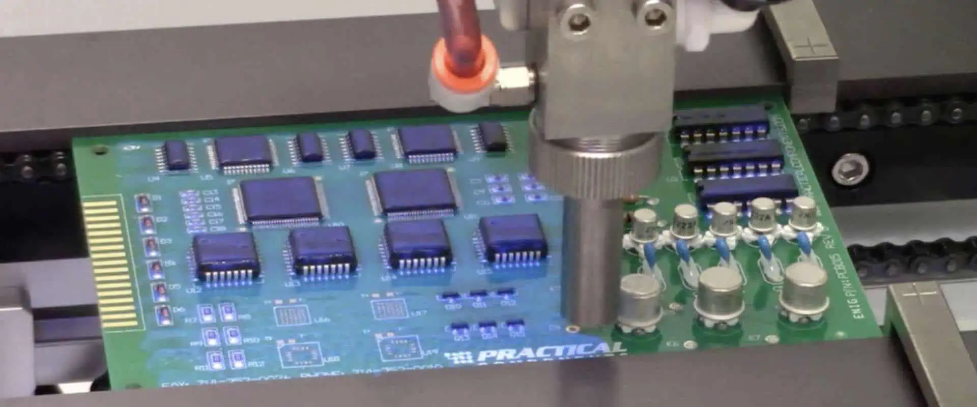
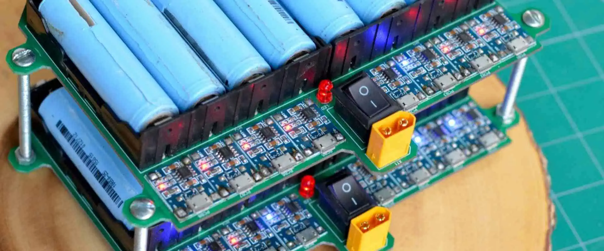
Printed circuit boards (PCBs) form the core of electronics products. Traces on the PCB conduct signals between components. If a trace gets damaged, it can disable the circuit. Instead of scrapping the PCB, trace damage can often be repaired. Specialized PCB trace repair kits provide materials and tools to fix broken traces quickly. This article provides a step-by-step guide to PCB trace repair using such DIY kits.

Overview of PCB Trace Repair Kits

PCB trace repair kits contain supplies to fix open or damaged traces and pads. A basic kit usually includes:

  • Conductive ink pen – repairs broken trace sections
  • Protective lacquer – isolates repaired areas
  • Precision tips – enable fine trace repairs
  • Cleaning accessories – prep surface before repair
  • Magnifier – helps detailed work

The core item is the conductive ink pen which recreates broken trace segments. The ink dries into a flexible conductive material repairing the electrical path. Other items aid the repair process.

More extensive kits add soldering accessories, replacement components, trace isolation materials, tools like tweezers and probes, and detailed manuals. However, even a basic kit with just the pens can fix many trace issues.

Example PCB trace repair kit

When to Repair Instead of Discarding PCBs

Common situations where PCB trace repair is worth trying instead of scrapping boards:

  • Prototyping – Fixing faults iteratively on prototype boards before final design.
  • Small Volume Boards – Unique/expensive boards where purchasing replacements has lead time and cost.
  • Legacy Boards – Old boards where replacements are unavailable.
  • Fast Turnaround – Faster to repair on-hand boards than order and wait for new ones.
  • Intermittent Issues – Flaky boards where problem is hard to reproduce.
  • Cosmetic Damage – Scrapes/nicks on surface that cut a trace completely.
  • Pad Repair – Missing pads prevent soldering components.

As long as the PCB substrate itself is intact, many types of trace-level damage can be repaired. This avoids unnecessary scrap costs.

Precautions When Repairing PCB Traces

Trace repair looks easy but requires care to succeed:

  • Review Schematics – Understand where the trace was routed and its connections.
  • Note Overall Damage – Assess if issues are limited to traces or more extensive.
  • Clean PCB – Remove all debris, residue and dust from repair area.
  • Magnify Work Area – Use a magnifier to clearly see fine traces.
  • Fine Control – Rest hands/arms to avoid shaking.
  • Verify Results – Inspect repair and test circuit before reassembly.

Rushing through repairs by taking shortcuts usually leads to failures. Careful attention to details ensures a working fix.

Step-by-Step Process for PCB Trace Repair

Here is a walkthrough of the trace repair process using a typical repair kit:

1. Assess Damage

  • Visually inspect the PCB to identify trace damage. Look for complete breaks in traces or scratched off areas.
  • Cross-check against board schematics to understand where the trace was routed and its connections.
  • Determine if surrounding areas are also damaged. Restrict repair to trace-level damage only.

2. Clean PCB Area

  • Clean the work area using the provided cleaning swabs/pads and alcohol solvent.
  • Remove all dirt, oxidation, residues or debris surrounding the damaged trace area.
  • Allow area to fully dry before continuing. Proper cleaning enables the repair to adhere.

3. Prepare Conductive Ink Pen

  • Select an appropriate tip size and attach it to the pen. Use finer tips for thin or intricate traces.
  • Shake the pen to mix the conductive ink which settles over time.
  • Prime the pen by pressing until ink flows out evenly. This prevents erratic flow.
  • Adjust ink flow if needed by turning the adjustment screw on the pen body.

4. Trace Repair Outline

  • Study the damaged trace path and determine where the ink will be applied to bridge the gap.
  • Lightly sketch along this path with a non-conductive pen as a guide for the actual conductive ink trace.

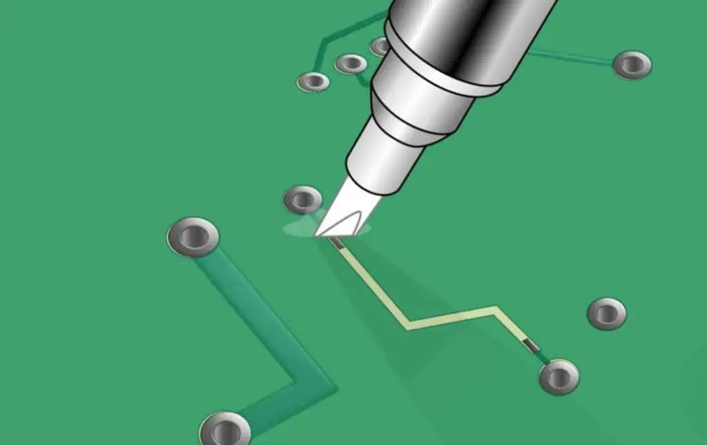
5. Apply Conductive Ink

  • Using the primed conductive ink pen, carefully draw a path following the outline to link the severed trace ends.
  • Try to recreate original trace dimensions – match width and follow original routing.
  • Overlap about 1 mm onto undamaged areas on each side for a robust joint.
  • Let ink fully dry. Apply a second pass if conductance is inadequate.

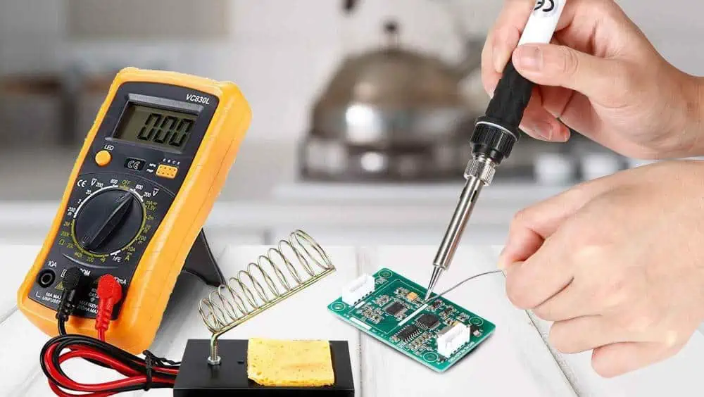
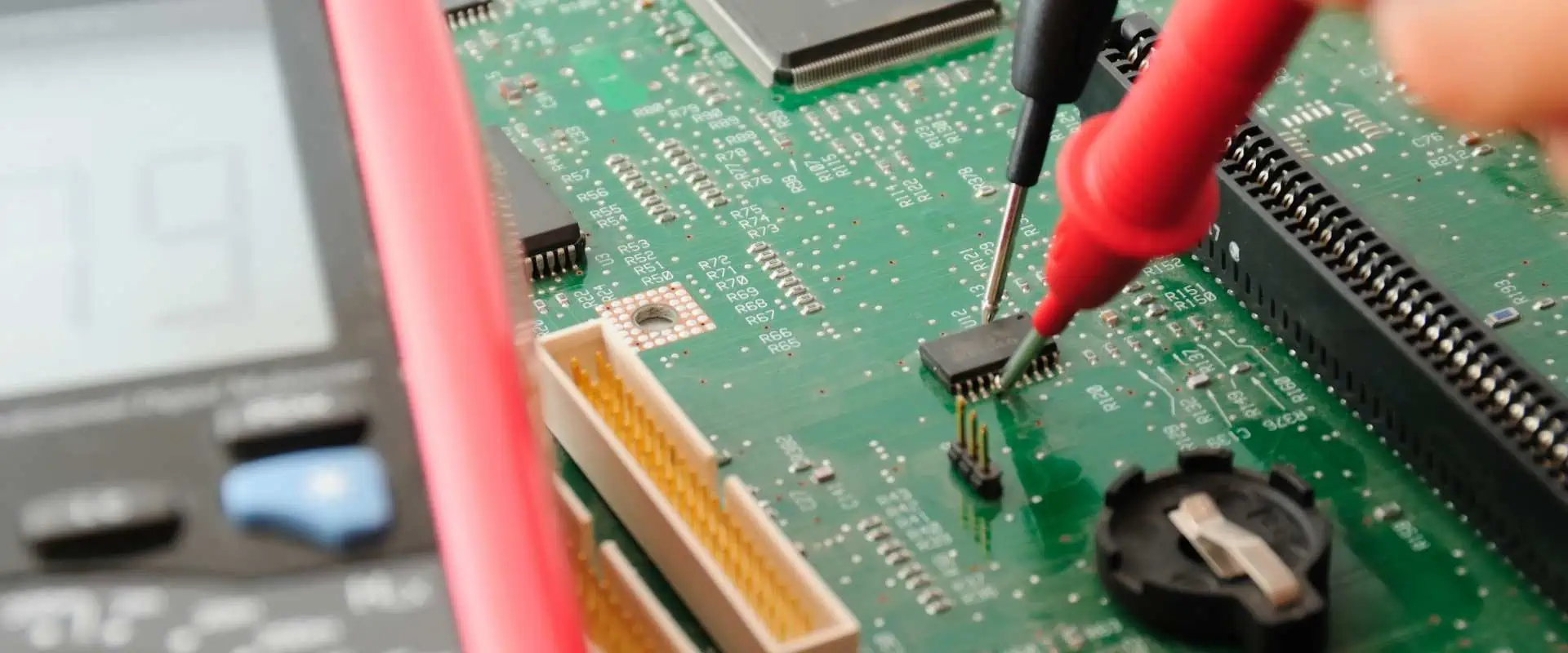
6. Test Conductivity

  • Use a multimeter or ohmmeter to check resistance along repaired trace. It should indicate continuity.
  • If no conduction, apply more ink over area to build up material. Let dry and recheck.

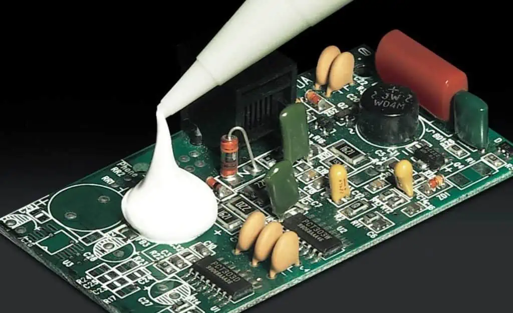
7. Apply Protective Coating

  • Paint a thin layer of the provided protective lacquer over the repaired region using an applicator.
  • Let protective coating dry fully to prevent smudging.
  • Optional step for extra isolation – helps prevent long term corrosion.

8. Reassemble and Test

  • If access permits, hand solder components to restored pads to verify conduction.
  • Fully reassemble the PCB and test its functionality. The circuit should operate normally now.

With practice, even intricate trace repairs can be executed reliably using this careful approach.

Tips for Repairing Different Trace Damage Cases

Besides complete breaks, various types of trace damage can occur. Here are tips for addressing each case:

Broken Trace

  • Bridge over the severed segment with conductive ink using multiple coats if needed for conductance.

Missing Pad

  • Rebuild pad area with conductive ink. Allow curing well to withstand soldering.

Damaged Solder Pad

  • Remove residual solder mask carefully using a craft knife. Repair pad outline with ink.

Scraped Trace Area

  • Lightly abrade scraped region to expose fresh conductor. Ink over it.

Partial Width Trace Scratch

  • Build up trace thickness along scratched portion using added ink coats.

Oxidized Copper Trace

  • Use fiberglass brush gently to reveal conductive copper before inking over.

With the right techniques, diverse trace damage scenarios can be successfully repaired.

Limitations of PCB Trace Repair

While trace repair kits are versatile, some limitations exist:

  • Very fine sub-1-mm traces are difficult to repair reliably.
  • Recreating complex pad geometries or dense via patterns may not be feasible.
  • Repairs lack long term robustness versus original copper traces.
  • Conductive ink pens have finite usage life and variable results.
  • Repairs are temporary if root cause of damage remains unaddressed.
  • Severe substrate damage affecting layers cannot be fixed.
  • High voltage, high frequency or precision analog circuits may not function properly after repair.
  • Insufficient cleaning and surface prep will undermine repair quality.

Understanding these caveats helps determine if repairing a particular board and type of damage makes sense over replacement.

Troubleshooting Common Trace Repair Issues

New PCB coating pen from Intertronics

Problems during trace repair are usually fixable with the right corrective measures:

IssuePossible CausesCorrective Actions
No conduction after repair– Insufficient ink thickness <br>- Ink smudged before drying <br>- Overlaps with undamaged areas inadequate– Apply more ink coats <br>- Allow each coat to dry fully before next <br>- Extend overlap with existing trace segment
Ink flows unevenly– Tip clogged <br>- Ink viscosity too high/low– Clean tip opening <br>- Adjust pen ink flow as needed
Repaired trace conducts initially but fails later– Flexing cracks ink trace over time <br>- Environmental exposure degrades ink– Reinforce with additional protective coating <br>- Minimize mechanical stress on repaired trace
Solder pad lifted during repair– Excessive heating during desoldering <br>- Aggressive scraping of residual mask– Use desoldering braid instead of hot air <br>- Remove mask carefully by scraping edges first
Repaired board functions inconsistently– Intermittent conduction along repaired area <br>- Unidentified damage elsewhere on board– Use multimeter to isolate conduction faults <br>- Thoroughly inspect board for any other issues needing repair

With good troubleshooting practices, most repair issues can be diagnosed and rectified.

Ensuring Long Term Reliability of Repairs

To improve long term reliability of trace repairs:

  • Flow slightly more ink than needed to create a robust conductor.
  • Overlap repaired and undamaged areas well for strong adhesion.
  • Apply protective coating to prevent corrosion over time.
  • Avoid mechanical stress on repaired trace – handle board carefully.
  • Periodically check repairs for deterioration and touch up if required.
  • If possible, run board at slightly lower than rated temperatures.
  • For very high reliability, consider having repaired boards professionally conformal coated.

With extra care during repair and follow-up maintenance, boards can function successfully long term following fixes.

PCB Trace Repair Alternatives

For damage beyond DIY repair capabilities, alternatives include:

Professional Repair Services – Many PCB assembly vendors offer repair services for complex damage. Useful for mission-critical boards.

Board Redesign – For systemic issues, re-designing the board with modifications may be better than repeated repairs.

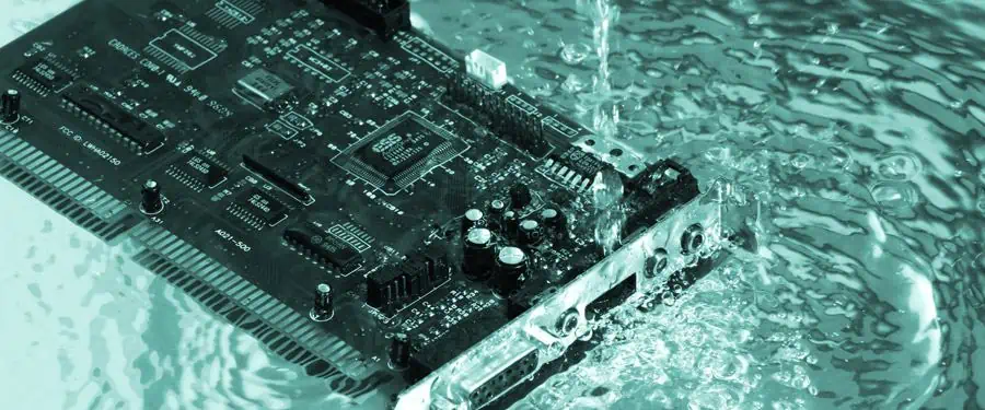
Board Protection – Conformal coatings, potting, protective enclosures can prevent future damage.

Better Handling Procedures – Many trace issues result from mishandling or weak packaging. Improving board handling minimizes damage.

Component-Level Repair – Swapping damaged components may be simpler than repairing traces.

Cabling – Using external cabling to bypass damaged areas on the PCB.

Combining DIY trace repairs for accessible issues and other solutions for severe damage provides a robust repair strategy.

Conclusion

PCB trace repair kits are a quick, affordable way to fix damaged traces and avoid discarding boards. With careful assessment of damage, preparation of the work area, precision use of conductive ink pens, and rigorous testing, broken traces can be restored successfully. Understanding repair limitations, troubleshooting issues, and implementing reliability best practices ensures long-lasting fixes. For optimal results, trace repair should be used alongside other mitigation approaches like enhanced handling procedures and board-level protection. By harnessing trace repair techniques, companies can save time and cost when dealing with damaged PCBs.

Frequently Asked Questions

Can solder mask repairs be done with trace repair kits?

No, the ink in basic kits is not formulated to adhere to solder mask surfaces. Special epoxy compounds and processes are required for solder mask repairs which most DIY kits do not provide.

How long does conductive ink take to dry?

Drying time depends on the ink chemistry, with most types drying within 5-10 minutes at room temperature. Curing can be accelerated by gently heating the board after ink application.

Can surface mount pads be repaired with these kits?

Yes, SMT pads can be reconstructed using the conductive ink but extra precision is required due to their small size. Allowing longer curing time improves durability for soldering.

Do the kits only work on copper traces?

The ink adheres well to copper so it works very effectively for copper traces. Performance will be degraded on other surfaces like gold or tin-plated traces.

How many times can a pen be used before replacing?

Dependent on the kit, each ink pen typically allows 10-25 repairs before needing replacement. Higher-end pens may enable more repairs. Checking conductivity after each repair detects any degradation in ink quality.

What is Silicone Conformal Coating For PCB ?

Introduction

Printed circuit boards (PCBs) are at the heart of electronics equipment providing the pathways for signals and power. However, PCBs are susceptible to contaminants, moisture, and temperature/humidity changes which can cause dendritic growth, corrosion, and short circuits. Applying a protective conformal coating on PCB assemblies safeguards against such damage and enhances reliability.

Silicone conformal coatings have emerged as a popular protective coating for PCBs due to their ability to repel water, provide insulation, and withstand wide temperature variations. This article provides an in-depth look into silicone conformal coatings, their properties, application methods, selection criteria, and benefits for PCB protection.

What is a Conformal Coating?

Conformal Coating

A conformal coating is a thin polymeric film applied on the PCB assembly to act as a barrier against contaminants like moisture, dust, chemicals, and temperature extremes. The conformal coating โ€œconformsโ€ evenly to the complex contours of PCB components, covering all surfaces.

Conformal coatings are dielectric (non-conductive) in nature to prevent shorting between adjacent traces and components on a crowded PCB. The coatings are applied in a thin layer – typically 25 to 200 microns thick. This protects the PCB without materially increasing weight or dimensions.

Some key functions of conformal coatings on PCBs are:

  • Prevent moisture ingress and chemical migration
  • Provide thermal and mechanical shock protection
  • Isolate high voltage areas on the PCB
  • Electrically insulate conductive elements from each other
  • Protect against dendritic growth between conductors
  • Reduce field failures and extend product life
YouTube video

Why Use a Silicone Conformal Coating?

Silicone conformal coatings provide distinct advantages that make them a popular PCB protection solution:

Hydrophobicity: Silicones have a highly hydrophobic (water repelling) nature. The water contact angle is over 90ยฐ for silicones. This property enables excellent moisture and condensation resistance.

Temperature stability: Silicone coatings retain their protective properties over a wide temperature range from -60ยฐC to 200ยฐC. They can withstand soldering temperatures.

Flexibility: Silicones have high elasticity to flex and absorb mechanical and thermal shocks. They resist cracking or chipping.

Dielectric strength: Silicones offer very high dielectric strength (>400V/mil) to insulate high voltage areas on PCBs.

Chemical resistance: Silicones are largely inert and resist a broad range of chemicals like acids, alkalis, and cleaning solvents.

Reparability: Silicone coatings can be selectively removed for rework using solvents without damaging the PCB components.

Processability: Liquid silicones are easy to apply on complex board geometries using spray or brush coating.

UL rating: Silicones can achieve UL 94 V-0 flammability rating – the highest standard.

In summary, the versatility, hydrophobicity, temperature resistance, flexibility, dielectric strength, chemical resistance, and processability make silicone an ideal conformal coating material for PCB protection.

Silicone Chemistry Overview

Silicone or polydimethylsiloxane (PDMS) is an inorganic polymer derived from silica (sand). It consists of a silicone backbone chain with organic methyl groups attached to the silicon atoms:

The Si-O bond gives high temperature stability, while the methyl groups (CH3) provide flexibility, hydrophobicity, and chemical inertness.

Varying the ratio of organic to inorganic content gives different silicone grades. Higher organic content imparts greater flexibility, while higher inorganic content increases hardness and temperature resistance.

Silicones containing reactive chemical groups can undergo further cross-linking to form protective conformal coatings. Moisture curing, UV curing, and thermal curing are popular methods to cure liquid silicones.

Types of Silicone Conformal Coatings

Silicone conformal coatings are available in one-part and two-part systems with different curing mechanisms:

1. One-Part Silicones

One-part silicones consist of siloxane polymers and cross-linking agents in a single container. They cure into solid films upon exposure to atmospheric moisture:

  • Acetoxy cure: Releases acetic acid as a byproduct while curing. Used where odor is not a concern.
  • Alkoxy cure: Releases alcohol, allowing low odor cure. Used for thick coatings.
  • Oxime cure: Cures via oxime linkages. Low odor but slower curing.

2. Two-Part Silicones

Two-part silicones consist of a base resin and a catalyst/curing agent in separate containers. They require mixing before application and cure:

  • Condensation cure: Base reacts with a tin, platinum or titanium catalyst. Fast curing, releases alcohol.
  • Addition cure: Uses a platinum catalyst to crosslink vinyl-functional polymers. Low odor, no byproducts.
  • UV Cure: Base resin cures under UV irradiation. Very fast cure speeds.

One-part silicones cure at room temperature upon exposure to ambient humidity. Two-part silicones provide more control over cure rate and properties.

Silicone Conformal Coating Properties

Silicone conformal coatings can be formulated in different viscosities from low viscosity liquids to thixotropic gels. Key properties include:

Viscosity: Liquid silicones have viscosity ranging from 300 to 1000 cPs, while gels are over 3500 cPs. Viscosity determines the coating thickness achievable.

Hardness: Silicones have Shore A hardness between 20 to 85 after curing. Softer grades are more flexible while harder grades are abrasion resistant.

Dielectric strength: Around 500 Volts/mil for most silicone coatings, enabling insulation of conductors with voltages differences.

Dielectric constant: 2.7 to 3.0 at 1 MHz frequency. Similar to PCB substrate materials.

Dissipation factor: Very low, 0.001 to 0.01 at 1 MHz showing minimal energy losses.

Volume resistivity: >10e15 Ohm-cm ensures electrical insulation.

Temperature range: Protective from -60ยฐC to 200ยฐC enables use under wide temperature swings. Withstands soldering heat.

Tensile strength: 200 psi and above makes silicone coatings tough and resistant to cracks/chips.

Elongation: Up to 150% elasticity allows silicones to bend and absorb stresses.

Flammability: Silicones achieve UL 94 V-0 rating – the highest flammability standard.

Moisture resistance: Silicones are highly hydrophobic with dielectric strength retained after 85ยฐC/85% RH exposure for over 1000 hours. Prevents corrosion and electrical leakage.

Chemical Resistance: Inert to most acids, alkalis, solvents etc. Allows cleaning and rework.

PCB Protection Applications of Silicone Conformal Coatings

Some major applications of silicone conformal coatings for PCB protection include:

Automotive Electronics: Protects against temperature extremes, vibration, moisture, and contaminants in under-the-hood automotive applications.

Power Supplies: Insulates high voltage PCBs and prevents arcing and short circuits in power supplies.

LED Lighting: Protects LED driver PCBs against moisture and corrosion. Maintains insulation resistance.

Control Equipment: Safeguards industrial control units in harsh plant environments against moisture, chemicals and particulate ingress.

Medical Electronics: Provides biocompatible, moisture-proof barrier for PCBs used in medical diagnostic equipment and body-worn devices.

IoT Devices: Extends service life of IoT endpoint devices deployed in uncontrolled ambient conditions exposed to spills, humidity, and pollutants.

Aerospace Avionics: Reliably insulates densely-packed PCBs on aircraft against vibration, shock, temperature swings, altitude changes etc.

Marine Electronics: Protects on-board electronics in marine vessels from salt spray, moisture condensation and water ingress.

Military Equipment: Ruggedizes electronics in battlefield conditions involving wide temperature variations, humidity, sand/dust ingress etc.

5G Telecom Gear: Maintains electrical isolation on sensitive RF PCBs against environmental contaminants.

Thus silicone conformal coatings safeguard PCBs across diverse operating environments and duty cycles throughout product lifecycle.

Benefits of Silicone Conformal Coatings on PCBs

Some key benefits offered by silicone conformal coatings to enhance PCB reliability are:

Moisture Resistance: Silicones provide a hydrophobic barrier preventing short circuits from dew condensation or water ingress.

Corrosion Prevention: The conformal coating isolates metal conductors from oxygen, moisture and contaminants to avoid corrosion.

Thermal Management: Silicones protect components from thermal extremes and minimize thermal shock damage due to their high flexibility.

Vibration/Shock Absorption: Cushions PCB assemblies from mechanical shocks and vibration through its damping properties.

Chemical Protection: Provides a barrier against splashes or leaks of chemicals like acids, solvents, fuels and alkaline cleaning agents.

Dendrite Prevention: Avoids growth of conductive dendrites between adjacent conductors that can cause shorting.

UV Resistance: Protects PCBs from damage by UV exposure during outdoor use.

Flame Retardancy: Silicone coatings achieve UL 94 V-0 rating to minimize fire hazard.

Electrical Isolation: Prevents arcing or short circuiting between closely spaced conductors due to the high dielectric strength.

Reworkability: Allows selective removal for repairs and rework without coating removal from the entire PCB.

Process Control: Liquid silicones are easy to apply on complex board geometries via spraying, brushing, or dipping.

Reliability: collectively, the protective properties enhance field reliability and extend service life of PCB assemblies.

Silicone Conformal Coating Application Process

Conformal Coating
Conformal Coating

A typical silicone conformal coating application process involves:

Surface Preparation

The PCB assembly is first cleaned to remove contaminants like dirt, oil or flux residues. An isopropyl alcohol (IPA) rinse cleans organic residues.

Programming Application Parameters

For automated Selective Coating Systems, the application parameters are programmed like coating area, thickness, speed etc.

Masking Sensitive Areas

Connectors, testpoints, and delicate components are masked using latex plugs or polymer tapes to prevent coating.

Mixing Two-Part Silicones

For two-part silicones, the resin and curing agent are precisely mixed just prior to application as per manufacturer instructions.

Coating Application

Liquid silicone is applied via spray coating, brushing, dipping or jetting based on PCB size and geometry. Uniform coverage is ensured.

Curing Process

The silicone coating is allowed to cure as a solid protective film, either at room temperature, with heat, or using UV lamps.

Unmasking and Inspection

After curing, masking materials are removed. The coating is visually inspected under brighter lighting for pinholes, thin spots or other defects.

Testing Protection Levels

The coated assembly may be subjected to insulation resistance, high voltage withstand, or other applicable tests.

Packaging for Shipment

The conformal coated board is then packed with moisture absorbents as needed for shipment to customers.

Selective Coating vs. Total Immersion

For high volume production, PCB assemblies are conformal coated using automated equipment:

Selective Coating uses programmable coating robots or mechanisms to deposit silicone only on the required areas, avoiding connectors or testpoints. This allows easy post-coating access.

Total Immersion dips the entire PCB assembly into a silicone bath to coat all surfaces. Additional steps may be needed to strip the coating from connectors and test areas.

Selective coating provides flexibility to customize the coating area for each board design. It consumes less coating material compared to total immersion. But total immersion allows very fast cycle times for high volume production.

Silicone Conformal Coating Selection Criteria

Key considerations for selecting a silicone conformal coating include:

  • Operating temperature range based on thermal loads on the PCB components and the application environment. Wide temperature range silicone coatings are preferred for versatility.
  • Flexibility levels based on mechanical stresses on the PCB. Softer, more flexible silicones cushion better against vibrations/shocks.
  • Hydrophobicity based on the level of moisture protection required. Higher water contact angle gives better moisture resistance.
  • Dielectric insulation needs based on conductor spacing and voltage isolation requirements on the PCB.
  • Coating thickness dictated by PCB component heights and conductor clearances. Thinner coatings 20-40 microns are suitable for most applications.
  • Viscosity should allow coating intricate PCB geometries. Thinner silicones with 300-1000 cPs viscosity are easier to apply on complex PCBs.
  • Cure speed required – one-part silicones for room temperature curing or two-part silicones for faster heat/UV curing.
  • Rework needs to remove and recoat certain sections if repairs are envisaged. One-part silicones allow simple rework using solvent stripping.
  • Outgassing requirements – for use in vacuum or hermetic environments, low outgassing silicones are chosen.
  • Biocompatibility for medical devices – specialized medical grade silicones are used.
  • Approvals like UL 94 V-0, IPC CC-830, RoHS compliance. Automotive grade silicones meet IATF 16949 standard.

Key Silicone Conformal Coating Manufacturers

Parylene Coating on PCB

Some leading manufacturers of silicone conformal coatings for PCB protection include:

  • Dow – SYLGARD conformal coatings
  • Shin-Etsu – KJR and KE Series silicone coatings
  • ACC Silicones – SILCOSET range of silicone coatings
  • Henkel – LOCTITE conformal coatings
  • Dow Corning – SE92XX silicone conformal coatings
  • Electrolube – UR5634 Underfill and Conformal Coating
  • Dymax Corporation – 9481 and 9482-LV silicones
  • MG Chemicals – 419 and 422 Series conformal coatings

These companies offer broad silicone conformal coating product lines catering to different PCB protection requirements across industry sectors with strong global technical support services.

Conclusion

Silicone conformal coatings deliver a unique combination of properties that make them ideally suited for protecting PCB assemblies from environmental and operational stresses. The hydrophobic nature, wide temperature range, high dielectric strength, chemical inertness, shock absorption, and easy application enable silicone coatings to safeguard the reliability of PCBs across diverse use conditions.

Both global manufacturers and local PCB assembly service providers offer a range of silicone coating products to suit specific application needs in terms of viscosity, flexibility, temperature resistance, dielectric rating, outgassing levels etc. By applying the optimal grade using controlled processes, silicone conformal coatings enhance the field reliability and extend service life of electronic systems.

Frequently Asked Questions

Q1. How does a silicone conformal coating protect a PCB?

Silicone coatings protect PCBs by:

  • Providing a moisture and chemical barrier
  • Electrically insulating high-voltage conductors
  • Absorbing mechanical and thermal shocks
  • Preventing growth of dendrites between traces
  • Shielding against environmental contaminants
  • Extending product reliability and lifespan

Q2. What are some key properties of silicone coatings?

Key properties include:

  • Hydrophobicity
  • Wide temperature range (-60ยฐC to 200ยฐC)
  • High flexibility and elongation
  • Excellent dielectric strength
  • Chemical and UV resistance
  • Thermal shock absorption
  • Flame retardancy

Q3. When should PCB assemblies be conformal coated?

Conformal coating should be applied when PCBs are used in:

  • High-humidity environments
  • Applications with large temperature swings
  • Presence of destructive contaminants or chemicals
  • Conditions prone to vibration/mechanical shock
  • High-voltage boards requiring insulation
  • Densely-packed boards susceptible to dendrite growth

Q4. How is silicone conformal coating applied to PCBs?

Typical application techniques include:

  • Selective spray coating using automated, programmable equipment
  • Dipping in silicone baths for total immersion
  • Manual brushing for coating selective areas
  • Jetting for precise coating of components
  • Self-healing silicones via microcapsules for repairable coatings

Q5. Can silicone coatings be removed for repairs/rework?

Yes, silicone coatings can be selectively stripped using solvents like xylene, toluene or THF for rework, without affecting the PCB. This allows easy repair of coated boards.

What is the difference between SMA and SMC connectors?

SMA and SMC connectors are two common radio frequency (RF) coaxial connector styles used in telecommunications, test equipment, aerospace, defense, and other microwave applications.

Both connector types provide excellent electrical performance at microwave and millimeter wave frequencies, but they have some distinct differences in their design and usage. Understanding these differences helps engineers select the right option for their specific application and performance requirements.

This comprehensive guide examines the key similarities and differences between SMA and SMC connectors in terms of design, performance, applications, standards and more.

SMA Connectors Overview

SMA (SubMiniature version A) connectors were introduced in the 1960s as a smaller alternative to Type N and C connectors used at the time. The SMA uses a snap-on coupling mechanism and offers broadband performance up to 18 GHz in some configurations.

Key Features

  • Compact threaded interface with snap-on coupling nut
  • Designed for semi-rigid and flexible cables
  • Widely used with test equipment, RF systems, microwave systems
  • Provides DC-18 GHz frequency range typically
  • Available in 50 ohm impedance
  • Robust mechanical design
  • Variants like reverse polarity SMA (RP-SMA)

SMA Connector

Where SMA Connectors are Used

SMA connectors are very popular for lower frequency microwave applications including:

  • Test and measurement equipment
  • Telecommunication equipment
  • Aerospace and military systems
  • Antennas
  • Medical devices
  • General purpose RF and microwave component interconnections

They are ideal for applications not requiring the ruggedness or precision of precision connectors. SMA strikes a good balance between performance, cost, and ease of use.

SMC Connectors Overview

SMC (SubMiniature type C) connectors were introduced in the 1980s as a smaller, higher performance alternative to SMA connectors. SMC uses a threaded coupling interface and offers excellent broadband performance to 26 GHz.

Key Features

  • Lightweight threaded coupling interface
  • Designed for semi-rigid cables
  • Stable performance to 26+ GHz
  • Broadband impedance of 50 ohms
  • Precision machined parts
  • Very low reflection coefficients
  • Attenuation comparable to 2.92mm connectors
  • Used for critical microwave connections

SMC Connector

Where SMC Connectors are Used

SMC connectors are well suited for high performance microwave applications including:

  • Aerospace and defense systems
  • Satellite communications
  • Test instrumentation
  • Microwave radio links
  • High speed data transmission
  • Laboratory equipment
  • Microwave component interfacing

Their precision and repeatability make them ideal for measurement, production, and field use in demanding environments.

SMA vs SMC Comparison

Now let’s look closely at how the two connector styles differ across various attributes:

ParameterSMA ConnectorSMC Connector
Frequency rangeDC – 18 GHzDC – 26 GHz+
Impedance50 ohms50 ohms
Connector interfaceThreaded coupling nutThreaded coupler
Coupling nut materialNickel plated brassStainless steel
DielectricPTFEPTFE
Body stylesStraight, bulkhead, jack, panel mountStraight, bulkhead
Durability500 mating cycles500+ mating cycles
RF leakageGood to 12 GHzExcellent to 18 GHz
IntermateabilityConnects with most SMAPrimarily mates with SMC
CostLow costHigher cost
Return lossAround -26 dB at 10 GHz-30 dB at 10 GHz
RepeatabilityModerateVery high
SizeLarger diameterMore compact
WeightHeavierLighter

As the table illustrates, SMC offers better electrical performance thanks to its precision design but at a higher cost and lower intermateability than SMA. Key differences are examined in more detail below.

Frequency Range

The SMA connector is intended for operation up to 18 GHz, while SMC provides excellent performance to 26 GHz and beyond. So for microwave applications above 18 GHz, the SMC is a better choice. Both connectors work very well at lower microwave frequencies.

Impedance

SMA and SMC connectors both provide 50 ohm coaxial impedance for matting with cables and components. This matches common RF system impedance.

Connector Interface

SMA uses a threaded coupling nut that snaps onto the receptacle so it can rotate independently. SMC utilizes a threaded coupler that engages directly with the receptacle interface.

This difference means SMA connectors tend to be easier to thread together, while SMC achieves better centering and microwave performance.

Coupling Nut Material

On SMA connectors the coupling nut is nickel plated brass. SMC uses passivated stainless steel for the coupler nut, improving corrosion resistance. Stainless steel also has less mass, reducing connector weight.

Dielectric Material

Both connector styles rely on PTFE (polytetrafluoroethylene) for the insulator dielectric material. PTFE provides excellent electrical properties at microwave frequencies along with chemical and temperature resistance.

Body Styles

SMA is available in a wider range of body configuration including straight, bulkhead, jack, panel mount and more. SMC tends to be offered in just straight and bulkhead connector versions.

Durability

The SMA and SMC are rated for approximately 500 mating cycles before performance degradation. This assumes proper mating and unmating procedures are followed. SMC provides a little better cycle life on average.

RF Leakage

SMC provides lower RF leakage than SMA, particularly at higher frequencies. This improves signal integrity and measurement accuracy. At 10 GHz SMC leakage is around -65 dB versus -55 dB for SMA.

Intermateability

Due to their different interfaces, SMA and SMC connectors are primarily intended to mate with same type. However, SMA connectors have some intermateability with Type N and 3.5mm connectors, while SMC connectors only reliably mate with other SMCs.

Cost

SMC connectors cost significantly more than SMA connectors, often 2-3 times as much. This is due to tighter tolerances and precision manufacturing of SMC components.

Return Loss

Return loss describes how much signal power is reflected back due to impedance mismatches in the connector. SMC provides excellent return loss of -30 dB or better at 10 GHz. SMA return loss is around -26 dB typically.

Repeatability

The SMC’s precision threaded interface allows greater mating repeatability than SMA. This ensures consistent performance over many connect/disconnect cycles.

Size

SMC connectors have a smaller diameter and take up less space than SMA connectors. SMC’s compactness provides more connector density in multi-connector assemblies.

Weight

Related to their size differences, SMC connectors are appreciably lighter than SMA models. This provides weight savings which are important in aerospace and portable applications.

SMA and SMC Standards

SMA and SMC connectors are standardized by different organizations:

  • SMA – MIL-PRF-39012, IEC 61169-42
  • SMC – MIL-PRF-39012, IEC 61169-65

These specifications define the critical dimensions, materials, electrical properties, environmental testing levels and other requirements that connectors must meet to be compliant.

Using connectors that adhere to the standards ensures interchangeability between suppliers and reliability in the field. The standards documents provide all the key technical details needed for manufacturers and users.

Typical Applications of SMA and SMC

SMA Applications

SMA connectors are very commonly used for:

  • Antenna connections
  • RF signal routing in wireless communications equipment
  • Interfacing test equipment like signal generators, spectrum analyzers, power meters and vector network analyzers
  • Microwave component evaluation and prototyping
  • General purpose coaxial jumpers and adapters
  • Lower frequency aerospace and defense electronics
  • Biomedical instruments like MRI machines

SMC Applications

SMC connectors are an excellent choice for:

  • High performance aerospace and defense communications
  • Fast data collection systems
  • Microwave instrumentation and metrology
  • High frequency antenna feeds
  • Satellite payloads
  • Microwave radio links
  • Calibrated measurement port extensions
  • Research labs and test facilities
  • Microwave component characterization

So SMCs are often found where accuracy, precision, and repeatability are paramount.

SMA and SMC Cable Assemblies

SMA and SMC connectors are frequently used on coaxial cable assemblies and adapters for interfacing equipment. Common cable types assembled with the connectors include:

Cable TypeDescriptionSMA UseSMC Use
Semi-rigid coaxSolid inner conductor with dielectric/outer conductor tubingCommonMost common
Flexible coaxCenter wire, dielectric, braided outer conductorCommonModerate use
WaveguideRectangular or circular metallic tubeVia adaptersVia adapters
Multi-cableMultiple coaxial lines bundled togetherYesLimited use

Semi-rigid cables are the preferred medium for both connectors. Flexible coax is more often used with SMA. Custom cable lengths, connector orientation, and configurations can be fabricated for various applications.

Choosing Between SMA and SMC

So when selecting between SMA and SMC connectors, consider the following:

Frequency Range โ€“ For applications over 18 GHz, SMC is likely the better choice. Under 18 GHz, either will work well.

Precision โ€“ If repeatability and accuracy under mating/unmating is critical, opt for SMC.

Performance โ€“ SMC provides lower reflection, leakage, and loss, so for demanding applications it is preferred.

Cost โ€“ SMA costs less than SMC, so use SMA if budget is a major factor and performance requirements are moderate.

Size โ€“ If a compact, lightweight connector is required, SMC is the smaller choice.

Environment โ€“ SMC offers better corrosion resistance for outdoor and humid applications.

Both connector families have proven reliability though, so performance tradeoffs, cost, and other factors specific to the application should all be weighed.

Conclusion

SMA and SMC connectors provide interconnect solutions across DC to 26+ GHz frequencies, with some important differences. SMA offers a balance of modest size, weight, cost and performance. SMC provides top-tier electrical performance for critical microwave connections, with tighter tolerances and somewhat higher cost.

Engineers have the luxury of choosing between two excellent coaxial connector platforms in SMA and SMC. By understanding their capabilities, limitations, and tradeoffs, informed design decisions can be made matching the connector technology to the demands of the application. Both SMA and SMC will continue serving the RF and microwave community well into the future.

Frequently Asked Questions

Here are some common FAQs about SMA and SMC connectors:

Q: Can SMA and SMC connectors be mated together?

A: Direct mating is not recommended. The different interfaces can cause damage. Adapters can allow interconnection in certain cases.

Q: How are SMA and SMC connectors identified when disconnected?

A: SMA has a larger nut with knurled brass surface. SMC uses a stainless steel threaded coupler. Visual markings also differentiate.

Q: What causes wear out in SMA and SMC connectors?

A: Debris entering the precision interface, contamination, exposure to weather extremes, improper mating, excessive mating cycles, etc. Proper care improves longevity.

Q: What torque should be used when tightening SMA and SMC connectors?

A: SMA is typically torqued to 4-5 in-lbs. SMC uses a lighter 0.9 in-lbs torque to avoid deforming precision threads.

Q: Can SMA or SMC connectors be used above 40 GHz?

A: Performance declines dramatically above 26 GHz for SMC and 18 GHz for SMA as coaxial modes are cut off. Other connector styles like 2.92mm are better beyond 40 GHz.

What Are Breakout Boards / SMT Breakout PCB ?

A breakout board (BOB) is a simple printed circuit board that allows access to the pins or leads on a surface-mount device (SMD or SMT) package. Breakout boards provide an easy way to prototype, test, or use an SMT component in a breadboard or through-hole application. They serve as an intermediate mounting platform to convert fine-pitched SMT components into more accessible thru-hole pins and connectors.

What Are SMT Components?

SMT, or surface-mount technology, refers to the method of mounting electronic components directly onto the surface of PCBs rather than with wire leads that pass through holes. Typical SMT component packages include:

  • Quad Flat Packages (QFP)
  • Ball Grid Arrays (BGA)
  • Tiny chip-scale packages like 0201 and 01005
  • Connectors like SMA, SMP, and uSD
  • Sensors, oscillators, resistors, capacitors

SMT enables great size reduction versus through hole components. However, the small size and dense connection pins also limit accessibility for prototyping. This is where breakout boards come in.

What Are Breakout Boards?

Breakout boards provide these key functions:

  • A simple PCB that an SMT component is mounted on
  • The dense SMT footprint is “broken out” into accessible through-hole pins
  • Allows easy connection of SMT parts to breadboards or cables for prototyping

Breakout boards make working with SMT components quick and easy for prototyping or testing, without requiring reflow soldering. They also enable easy incorporation of SMT parts into through-hole projects.

Typical Breakout Board Features

Breakout boards implement various features to improve usability:

  • Through-hole pins – The dense contacts of chips are converted to widely spaced pins.
  • Header sockets – Pin rows connect to standard 0.1″ pitch headers/connectors.
  • Castellated edges – Allow soldering wires directly to board edge.
  • Silkscreen labels – Identify pin names/numbers for reference.
  • Pad numbering – Match pinout diagrams on datasheets.
  • Test points – Exposed metal pads for multimeter probes.
  • Mounting holes – Allow securing board with standoffs.
  • Polarization keys – Help correctly orient polarized components.

Applications and Uses of Breakout Boards

Breakout boards are indispensable tools for working with SMT components in prototyping:

  • Interfacing SMT ICs – Quickly interface any SMT microcontroller, sensor, memory chip, etc.
  • Simplifying designs – Avoid complexity of mixing SMT and through-hole assemblies.
  • Testing and characterization – Convenient points to connect test probes and instruments.
  • SMT integration for hobbyists – Incorporate advanced SMT parts in DIY electronics projects.
  • Temporary adapter boards – Provide access to SMT parts for repair/reworging of consumer electronics.
  • Education – Allows students to easily experiment with SMT components with minimal tools and experience.

Types of Breakout Boards

There are a few common types and categories:

Generic Boards

  • SMT Carrier Boards – Accept a range of chip sizes from 0201 to QFN with changeable adapter sockets.
  • Universal Breakout Boards – Array of connect pads for hand-soldering SMT parts.

###chips.

  • Microcontroller Boards – Break out pins of SMT MCUs like ESP32, STM32, etc.
  • Sensor Boards – For SMT sensors like IMUs, magnetomers, PMICs.
  • Memory Boards – SD cards, EEPROMs, flash storage chips.
  • RF and Wireless Boards – Bluetooth, WiFi, GSM, NFC modules.
  • Display and LCD Boards – OLED, TFT displays.
  • Audio Boards – For SMT codecs, amps, DAC/ADC chips.

Any specialized SMT component can have a matching breakout board for easy interconnection.

How Are Breakout Boards Manufactured?

Specialized PCB assembly is used to mount SMT components onto breakout boards:

  • SMT Assembly – Pick-and-place machines precisely mount the chips using solder paste and reflow.
  • Selective wave soldering – Adds through-hole pins to bottom side after SMT loading.
  • Hand assembly – For quick prototyping, chips can be hand-soldered to blank generic boards.
  • Rework and QC – Optical inspection and rework of bridges or tombstoned parts.
  • Conformal coating – Protective epoxy layer prevents accidental short circuits.

Fully assembled boards with mounted SMT parts are available from electronics suppliers. But blank boards allow hand-assembly for custom parts.

Design Considerations for Breakout Boards

Several factors are considered when designing breakout boards:

  • Original footprint – Matching the SMT part’s datasheet footprint exactly.
  • Pad spacings – Sufficiently wide gaps between edge connection pads.
  • Routing channels – Areas clear of copper between pads for isolating signals.
  • Pinouts – Arranging edge pins to match reference designs.
  • Pin labeling – Clear silkscreen numbering matching datasheets.
  • Board shape/size – Rectangular or circular board large enough for part.
  • Mounting holes – Including fastening points if needed for stability.
  • Stackup – 4-layer boards with power/ground planes for high-frequency parts.

Careful breakout board design ensures the SMT component connects properly and signals are cleanly routed.

Creating Custom Breakout Boards

For highly specialized SMT parts, engineers may design custom breakout boards tailored to an exact application:

Design Process

  • Obtain datasheet for target SMT component
  • Import footprint into PCB CAD tool as new component
  • Arrange I/O pins on edges with spacings for connectivity
  • Add text labels, markers, mounting holes as needed
  • Export Gerber files of finished board layout

Manufacturing

  • Send Gerber files to trusted PCB fabrication vendor
  • Source compatible SMT components for assembly
  • Ship SMT parts and blank boards to assembly contractor
  • Have assembled boards delivered with mounted components

While more complex than generic boards, custom breakout PCBs enable specialized SMT components to be easily utilized in prototype projects.

Integrating Breakout Boards in Prototyping

Breakout boards are easy to integrate into electronics projects:

  • Solderless – Insert header pins into breadboard or use jumper wires for no-solder prototyping.
  • Soldered wires – Solder solid core wires directly to edge pads for semi-permanent connections.
  • Castellated edges – Allows soldering jumper wires neatly to board edge.
  • Stacking headers – Female headers on multiple boards stack together when prototyping complex circuits.
  • Screw terminals – Some boards provide screw terminals for field wiring.

With standardized pin spacing, breakout boards drop into breadboards or custom circuits easily.

Sourcing Breakout Boards

Many online retailers offer a wide selection of ready-made breakout boards:

  • SparkFun – Extensive catalog of over 1500 boards for most common SMT ICs and modules.
  • Adafruit – Another leading provider carrying 1000+ boards. Very beginner friendly.
  • Seeed Studio – Manufacture and sell many different breakout boards.
  • Tindie – Marketplace for unique products has breakouts made by DIY creators.
  • eBay/AliExpress – Cheap boards of common parts can be sourced directly from China. Quality varies.

For unusual or custom SMT chips, consider having PCB assembly houses manufacture a custom breakout board to your requirements.

Pros and Cons of Using Breakout Boards

Breakout boards provide unmatched convenience and usability but also some limitations:

Advantages

  • Extremely easy to prototype without soldering skills.
  • Integrates SMT components into breadboard or through-hole designs.
  • Cost effective compared to using development boards.
  • Wide selection of ready-made boards available.

Disadvantages

  • Adds parasitic capacitance that may affect high frequency signals.
  • Less compact than direct SMT integration.
  • Costly for low volume or custom designs.
  • Limited availability for uncommon components.

Overall, breakout boards provide the simplest path to utilizing SMT chips in prototype development and education applications. Their accessibility enables incredible innovation.

Example Breakout Boards

To illustrate typical breakout board implementations and usage, here are some examples for common SMT components:

ESP32 Series Module

  • Breaks out GPIO, power, and serial pins on popular ESP32 WiFi/BT module.
  • 0.1″ pitch castellated connection pads for easy breadboard use.
  • USB-serial interface eliminates need for FTDI cable.
  • Ready to load MicroPython firmware out of the box.

BME680 Sensor

  • Exposes I2C pins for Bosch’s integrated environment sensor.
  • Test points provided to probe SDA, SCL lines.
  • Qwiic connector for plug and play connection to development boards.
  • Minimalist design focused on easy connectivity.

AT24C02B EEPROM

  • Dual row female pinheaders interface to standard jumper wires.
  • Address select pins broken out to dip switches.
  • Test pads provided for ICSP interface.
  • Simple and general purpose.

Frequently Asked Questions

What is the difference between a breakout board and a development board?

Breakout boards just provide connectivity for a single SMT component. Development boards integrate multiple ICs and peripherals with power regulation to create a complete system for building applications on top of.

Can I solder wires directly to a breakout board?

Yes, the row of pads along the edges of most breakout boards are designed for easy soldering of solid core wire jumpers. Having castellated edges allows soldering wires right to the PCB edge.

How are breakout boards different from adapter boards?

Adapter boards convert between different pinouts or form factors rather than SMT to through-hole. For example, converting DIP chips to work in breadboards or SIL pin headers to SIP sockets. The goal of accessing SMT specifically defines breakout boards.

Can I probe test points on a breakout board while a circuit is powered?

Use extreme caution, as probing powered test points risks short circuits. Add jumper wires from test points to measurement equipment inputs instead of direct probing whenever possible. Power off completely if probing is required.

What is the most flexible breakout board for prototyping many different SMT ICs?

Generic SMT carrier boards accept different sized adapter sockets allowing a wide range of chip packages to be used. However, customized boards for specific components offer higher quality signal routing.

How do you calculate the PCB Trace Resistance ?

The resistance of copper traces on printed circuit boards impacts power distribution, signal integrity and overall circuit performance. Accurately calculating trace resistance is therefore an important skill for PCB designers. This article will provide an overview of the key parameters and formulas used to determine trace resistance.

Factors Affecting Trace Resistance

The resistance of a PCB trace depends on several factors:

  • Trace Geometry – Dimensions like length, width and thickness. Longer, narrower and thinner traces have higher resistance.
  • Copper Properties – Resistivity and temperature coefficient depend on copper purity and alloy percentages.
  • Trace Shape and Path – Meandering traces have more resistance than straight lines.
  • Copper Surface – Surface roughness from etching impacts resistance.
  • Temperature – Copper resistance increases with temperature.
  • Operating Current – At high currents, resistance increases due to self-heating.

Accurately accounting for all these parameters helps predict the trace resistance seen in the actual PCB circuit.

Trace Resistance Calculation Fundamentals

The resistance of a PCB trace depends on its resistivity, length and cross-sectional area as described by:

$$R_{trace} = \rho \frac{L}{A}$$

Where:

  • Rtrace = Trace resistance in ohms (ฮฉ)
  • ฯ = Resistivity of copper (ฮฉ.m)
  • L = Length of the trace (m)
  • A = Cross-sectional area of trace (m2)

Resistivity (ฯ)

Resistivity is a material property indicating how strongly it opposes electric current flow. For copper, it is:

  • 1.72 x 10<sup>-8</sup> ฮฉ.m at 20ยฐC
  • Increases by 0.00393 per ยฐC above 20ยฐC due to temperature coefficient of copper.

Length (L)

Length is the end-to-end distance travelled by the trace in meters. This should account for any meandering of the trace.

Cross-sectional Area (A)

For a standard rectangular trace, the cross-sectional area is:

$$A = T \times W$$

Where:

  • T = Trace thickness in meters
  • W = Trace width in meters

This simple model allows us to approximate the resistance of basic straight trace geometries. However, real-world traces often have more complex shapes which require further considerations.

Advanced Modelling for Trace Resistance

To account for various complexities in PCB traces, advanced modelling techniques are required:

Accounting for Non-Straight Traces

For meandering traces, break the path into straight rectangular segments and calculate resistance piece-wise before summing.

Accounting for Varying Widths

For traces with varying widths, break into segments of constant width and sum the resistances.

Accounting for Internal Layers

Traces in inner layers have reduced surface roughness. Use adjusted resistivity values.

Accounting for Self-Heating

At high currents, use incremental resistance ratios to model self-heating.

Accounting for High Frequencies

Consider skin and proximity effects that redistribute current at high frequencies.

Accounting for Non-Uniform Thickness

Use minimum expected thickness in calculations to account for fabrication variations.

Accounting for Surface Roughness

Model the uneven copper surface as a correction factor to the area.

Using 3D EM Simulation

For precision modelling, use 3D electromagnetic simulation of the entire trace shape.

By utilizing these advanced modelling techniques, very accurate estimation of trace resistances can be obtained.

Calculating Single-Layer Trace Resistance

For simple rectangular traces on a single layer, we can apply the fundamental resistance equation:

Example

Calculate resistance of a 200mm long, 0.5mm wide trace in 1oz (35ฮผm) copper.

Known:

  • Length (L) = 0.2 m
  • Width (W) = 0.0005 m
  • Thickness (T) = 35 x 10<sup>-6</sup> m (1oz)
  • Resistivity of Copper (ฯ) = 1.72 x 10<sup>-8</sup> ฮฉ.m

Cross-sectional Area (A)

A = T x W = (35 x 10<sup>-6</sup>) x (0.0005) = 17.5 x 10<sup>-6</sup> m<sup>2</sup>

Applying resistance equation:

Rtrace = (ฯ x L) / A = (1.72 x 10<sup>-8</sup> x 0.2) / 17.5 x 10<sup>-6</sup> = 0.0196 ฮฉ

Therefore, resistance of the 200mm long, 0.5mm wide trace in 1oz copper is 0.0196 ฮฉ.

This approach allows quickly estimating single-layer rectangular trace resistances.

Multi-Layer Trace Resistance Calculation

For traces passing between layers in a multi-layer PCB, adjustments are needed in the resistance calculations:

Accounting for Via Resistance

Add the resistance of vias connecting adjacent trace sections.

Accounting for Inter-Layer Dielectric

Account for dielectric thickness between layers when summing segment lengths.

Using Layer Adjusted Resistivity

Inner layers have smoother copper so lower resistivity. Outer layers are rougher.

Example Multi-Layer Calculation

  • 200mm long trace with 100mm on top layer and 100mm on inner layer
  • 2 vias connecting layers, each 0.1mm diameter, 0.2mm length
  • 0.5mm trace width
  • 1oz (35ฮผm) copper on outer layers
  • 1oz (35ฮผm) + 18ฮผm copper on inner layer
  • FR-4 dielectric between layers, 0.2mm thick

Via Resistance

Rvia = 2 x ฯCu x Lvia / Avia
= 2 x 1.72×10<sup>-8</sup> x 0.2 / (ฯ€ x (0.1/2)<sup>2</sup>) = 0.0079 ฮฉ

Outer Layer Trace

Rtop= ฯCu x Ltop / Atop
= 1.72×10<sup>-8</sup> x 0.1 / (35×10<sup>-6</sup> x 0.0005) = 0.0098 ฮฉ

Inner Layer Trace

Rinner = ฯCu x Linner / Ainner = 1.52×10<sup>-8</sup> x (0.1+0.2) / (35×10<sup>-6</sup>+18×10<sup>-6</sup>) x 0.0005
= 0.0067 ฮฉ

Total Resistance

Rtotal = Rtop + Rvia + Rinner = 0.0098 + 0.0079 + 0.0067 = 0.0244 ฮฉ

This demonstrates how to account for vias and different layers when calculating overall trace resistance for a multi-layer PCB.

Trace Resistance Calculation Tool

Manually applying the equations can get tedious. For convenience, online trace resistance calculators allow specifying all the parameters needed and provide the computed resistance.

Here is an example screenshot of a browser-based calculator:

These tools provide a quick and easy way to estimate trace resistances for your PCB designs.

Effects of Temperature on Trace Resistance

12 Functions of Zero Ohm (ฮฉ) Resistance

Due to the positive temperature coefficient of copper, resistance of traces increases with temperature:

Temperature Coefficient of Copper

Around 0.00393 ฮฉ/ฮฉ/ยฐC

Temperature Adjusted Resistivity

ฯT = ฯ20ยฐC [1 + ฮฑ (T – 20ยฐC)]

Where:

  • ฯT = Resistivity at temperature T
  • ฯ20ยฐC = Resistivity at 20ยฐC (1.72 x 10<sup>-8</sup> ฮฉ.m)
  • ฮฑ = Temperature coefficient (0.00393 for copper)
  • T = Actual operating temperature in ยฐC

This adjusted resistivity is then used in resistance calculations to account for temperature.

Example

A 50mm long, 0.25mm wide trace experiences 50ยฐC temperature rise during operation. Initial resistance at 20ยฐC is:

R20ยฐC = ฯ20ยฐC x L / A
= 1.72 x 10<sup>-8</sup> x 0.05 / (0.035 x 0.00025) = 0.0049 ฮฉ

Resistance at 70ยฐC is:

ฯ70ยฐC = 1.72 x 10<sup>-8</sup> [1 + 0.00393 x (70 – 20)] = 2.012 x 10<sup>-8</sup> ฮฉ.m

R70ยฐC = ฯ70ยฐC x L / A
= 2.012 x 10<sup>-8</sup> x 0.05 / (0.035 x 0.00025) = 0.0058 ฮฉ

The temperature rise has increased the trace resistance by 18%.

Impact of Trace Resistance

The resistance of PCB traces has several important effects on circuit performance:

  • Voltage drops along traces carrying high currents – can affect device operation.
  • Power loss and heating due to current flow – impacts thermal design.
  • Signal degradation and delays – limits maximum trace lengths for signals.
  • Impedance discontinuities – affects signal integrity especially for high-speed signals.
  • Noise pickup – higher resistance traces are more susceptible.

Hence considering trace resistance and mitigating its impact is crucial during PCB design to ensure proper functioning of circuits.

Techniques to Reduce Trace Resistance

Here are some methods to minimize trace resistance on PCBs:

  • Use thicker copper – 2oz and 3oz copper significantly reduce resistance.
  • Increase trace widths for power traces carrying higher currents.
  • Use shorter and straighter trace routing. Avoid meandering paths.
  • Use inner PCB layers which have smoother copper.
  • Use wider power/ground planes to distribute current.
  • Maintain lower ambient operating temperatures.
  • Coat traces with low-resistance silver, gold or tin alloys.

With careful design, the impact of inherent copper trace resistance can be mitigated, enabling high-performance PCB implementation.

Conclusion

  • The resistance of printed circuit board traces depends on resistivity of copper, trace length and cross-sectional area.
  • Advanced modelling techniques are needed to account for complex real-world trace geometries and multi-layer boards.
  • Trace resistance impacts power distribution, thermal design and signal integrity.
  • Careful calculations coupled with mitigation techniques help overcome limitations of inherent copper resistivity.

Top 5 FAQs on Calculating Trace Resistance

Q1: How accurate are simple trace resistance calculations?

For straight rectangular traces, the simple resistance equation provides a good estimate. Real-world complex traces require advanced modelling for accuracy.

Q2: Do wider traces always have lower resistance?

Yes, for the same thickness, increasing trace width reduces resistance. But wider traces have higher capacitance impacting signals.

Q3: Does trace length include bends and meanders?

Yes, total end-to-end length following the entire trace path must be used, not just linear distance between endpoints.

Q4: Can increasing copper thickness eliminate resistance issues?

Thicker copper helps reduce resistance but is limited by manufacturability and costs. Wide traces still provide lower resistance for power distribution.

Q5: What precision of trace resistance calculation is needed?

1-5% accuracy is sufficient for most needs. Precise modelling is required where resistance impacts impedance matching, voltage drops or thermal management.

How to Use a Soldering Iron for PCB Repair: Tips, Techniques & Safety

Printed Circuit Board (PCB) repair is an essential skill for electronics enthusiasts and professionals alike. At the heart of this process is the PCB soldering iron, a versatile tool that allows you to make precise connections and repairs. In this comprehensive guide, we’ll walk you through the steps of using a PCB soldering iron effectively, provide valuable tips and techniques, and emphasize important safety considerations.

Understanding the PCB Soldering Iron

Before diving into the repair process, it’s crucial to familiarize yourself with the PCB soldering iron and its components.

What is a PCB Soldering Iron?

A PCB soldering iron is a hand-held tool used to melt solder, allowing you to join electronic components to a printed circuit board or repair existing connections. It consists of a heated metal tip and an insulated handle.

Key Components of a PCB Soldering Iron

  1. Heating Element: Generates heat to melt the solder
  2. Tip: The pointed end that transfers heat to the solder and components
  3. Handle: Insulated grip for safe handling
  4. Power Cord: Connects the iron to a power source
  5. Temperature Controlย (on some models): Allows adjustment of the tip temperature

Preparing for PCB Soldering

PCB soldering problems

Proper preparation is key to successful PCB repair. Follow these steps to set up your workstation and prepare your PCB soldering iron.

Setting Up Your Workstation

  1. Choose a well-ventilated area with good lighting
  2. Use a heat-resistant work surface
  3. Keep a soldering iron stand nearby
  4. Have a damp sponge or brass wool tip cleaner ready

Preparing Your PCB Soldering Iron

  1. Inspect the iron: Check for any damage to the cord or handle
  2. Choose the right tip: Select a tip size appropriate for your task
  3. Clean the tip: Use a damp sponge or brass wool to clean the tip
  4. Tin the tip: Apply a small amount of solder to the tip to improve heat transfer

Read more about:

Step-by-Step Guide to Using a PCB Soldering Iron

Circuit board solder iron

Now that you’re set up, let’s go through the process of using a PCB soldering iron for repair work.

Step 1: Power On and Set Temperature

  1. Plug in your PCB soldering iron
  2. If your iron has temperature control, set it to the appropriate temperature for your solder (usually around 315-370ยฐC for lead-free solder)
  3. Allow the iron to heat up fully (usually takes 2-3 minutes)

Step 2: Prepare the PCB and Components

  1. Clean the PCB surface with isopropyl alcohol
  2. Identify the area that needs repair
  3. If replacing a component, remove the old one using desoldering techniques

Step 3: Apply Flux (Optional but Recommended)

  1. Use a flux pen or apply a small amount of liquid flux to the joint area
  2. Flux helps the solder flow and creates stronger joints

Step 4: Position the PCB Soldering Iron

  1. Hold the iron like a pencil, close to the tip for better control
  2. Place the tip of the PCB soldering iron so it contacts both the pad and the component lead

Step 5: Apply Solder

  1. Touch the solder to the joint, not directly to the iron tip
  2. The solder should flow smoothly onto the pad and component
  3. Use just enough solder to form a small, concave fillet

Step 6: Remove Heat and Allow Cooling

  1. Remove the solder first, then the PCB soldering iron
  2. Hold the board still for a few seconds to allow the joint to cool and solidify

Step 7: Inspect the Joint

  1. A good solder joint should be smooth, shiny, and concave
  2. Look for complete wetting of the pad and component lead

Step 8: Clean Up

  1. Clean any flux residue with isopropyl alcohol
  2. Trim any excess component leads

Advanced PCB Soldering Iron Techniques

Once you’ve mastered the basics, try these advanced techniques to improve your PCB repair skills.

Drag Soldering for Surface Mount Devices (SMDs)

  1. Apply flux to all pads
  2. Add a small amount of solder to the PCB soldering iron tip
  3. Drag the iron across the pins, allowing surface tension to separate the solder

Reflowing Solder

  1. Apply flux to the existing solder joint
  2. Heat the joint with the PCB soldering iron until the solder melts and reflows
  3. Remove the iron and allow the joint to cool

Using a PCB Soldering Iron for Desoldering

  1. Apply fresh solder to the joint you want to remove
  2. Heat the joint with the PCB soldering iron
  3. Use a solder sucker or desoldering braid to remove the molten solder

Tips for Effective PCB Soldering Iron Use

Improve your PCB repair skills with these helpful tips:

  1. Keep the tip clean: Regularly wipe the tip on a damp sponge or brass wool
  2. Maintain proper temperature: Too low, and the solder won’t flow; too high, and you risk damaging components
  3. Use flux: Flux improves solder flow and joint quality
  4. Practice good technique: Apply heat to the joint, not the solder
  5. Choose the right solder: Use appropriate solder for your application (lead-free for most modern electronics)
  6. Invest in quality tools: A good PCB soldering iron makes a significant difference in your work

Safety Considerations When Using a PCB Soldering Iron

Male hands solder components onto a printed circuit board using copper and a soldering iron. Electronics repair. Selective focus.

Safety should always be your top priority when working with a PCB soldering iron.

Personal Protective Equipment (PPE)

  1. Wear safety glasses to protect your eyes from solder splatter
  2. Use a fume extractor or work in a well-ventilated area to avoid inhaling solder fumes
  3. Consider wearing heat-resistant gloves for additional protection

Safe Handling of the PCB Soldering Iron

  1. Always return the iron to its stand when not in use
  2. Never leave a powered-on iron unattended
  3. Allow the iron to cool completely before changing tips or storing

Workspace Safety

  1. Keep your soldering area clean and organized
  2. Use a fire-resistant work surface
  3. Have a first aid kit nearby in case of minor burns

Troubleshooting Common PCB Soldering Iron Issues

Even experienced technicians encounter issues. Here’s how to address common problems:

Cold Solder Joints

Problem: Joint appears dull and grainy Solution: Reheat the joint and add a small amount of fresh solder

Solder Bridges

Problem: Solder connects two points that should be separate Solution: Use desoldering braid to remove excess solder

Lifted Pads

Problem: Copper pad separates from the PCB Solution: Carefully glue down the pad and use wire to make the connection

Overheating Components

Problem: Component becomes too hot during soldering Solution: Use a heat sink or reduce soldering time and temperature

Maintaining Your PCB Soldering Iron

Proper maintenance extends the life of your PCB soldering iron and ensures consistent performance.

Daily Maintenance

  1. Clean the tip before and after use
  2. Tin the tip before storage to prevent oxidation

Long-Term Maintenance

  1. Replace the tip when it becomes pitted or worn
  2. Check the cord for any signs of wear or damage
  3. Calibrate temperature-controlled irons periodically

Conclusion: Mastering the Art of PCB Soldering Iron Use

Using a PCB soldering iron effectively is a skill that improves with practice. By following the steps and tips outlined in this guide, you’ll be well on your way to becoming proficient in PCB repair. Remember to prioritize safety, maintain your equipment, and continuously refine your technique.

Whether you’re a hobbyist working on DIY projects or a professional in the electronics industry, mastering the use of a PCB soldering iron is an invaluable skill. With patience and persistence, you’ll be able to tackle even the most challenging PCB repair tasks with confidence.

Keep practicing, stay curious, and never stop learning about new techniques and technologies in the world of PCB repair. Your expertise with a PCB soldering iron will prove to be an asset in countless electronic projects and repairs.

What is PCB on 18650 Battery?

18650 batteries are cylindrical lithium-ion batteries that are commonly used in high drain devices like laptops, electric vehicles, and high-powered flashlights. At one end of the 18650 battery is the positive terminal, and at the other end is the negative terminal. In between the terminals is the PCB or protection circuit board.

The PCB serves some important functions:

  • Prevent over-charging and over-discharging of the battery
  • Protect against short circuits
  • Control current flow in and out of the battery
  • Provide a connection point for the terminals

Understanding what the PCB is and how it works is useful for anyone using 18650 batteries. This article will provide a detailed overview of the PCB on 18650 batteries.

What is a PCB?

PCB stands for Printed Circuit Board. A PCB is a thin board made of fiberglass or other composite materials that has copper tracings etched into it. Electronic components such as resistors, capacitors, and integrated circuits are mounted and soldered onto the PCB to create an electronic circuit.

A typical PCB with electronic components mounted on it

PCBs provide a sturdy base for mounting delicate electronic components and copper tracings to route electrical signals between components. PCBs are invaluable in all electronic devices, enabling compact and reliable construction.

PCB on 18650 Battery

18650 battery with protection circuit module attached

The PCB on an 18650 battery, also called a protection circuit module (PCM), serves the same purpose as a PCB in other electronic devices – it routes electrical connections and mounts electronic components. However, the PCM in an 18650 battery has some additional important functions:

Overcharge Protection

When charging, lithium-ion batteries must not be charged beyond their safe voltage range, which is typically 4.2V for most 18650 cells. The PCM contains an overvoltage protection circuit that monitors the battery voltage and disconnects the battery from the charger if the voltage exceeds the safe limit. This prevents the battery from being damaged by overcharging.

Overdischarge Protection

When discharging, lithium-ion batteries must not be drained below a certain voltage threshold, around 2.5-3V for most 18650 cells. The PCM contains an undervoltage protection circuit that monitors the battery voltage and disconnects the load if the voltage drops too low. This prevents the battery from being damaged by over-discharging.

Short Circuit Protection

Short circuits can draw huge currents and overheat batteries. The PCM contains current limiting circuitry such as fuses and PTC thermistors that cut off the current if a short circuit is detected. This protects the battery from excessive current.

Cell Balancing

In multi-cell battery packs, the cells can become imbalanced over time – one cell can become overcharged/overdischarged compared to the other cells. The PCM contains cell balancing circuits that keep the cells at equal voltage and charge levels for optimal performance and life.

Terminals

The positive and negative battery terminals are connected to the PCM, which routes the current in and out of the battery. So the PCM provides easily accessible battery terminals for devices to connect to.

Protection Circuit Components

The protection circuits on the PCM are created with various electronic components that perform specific functions:

MOSFETs

MOSFET symbol

MOSFETs (Metal-Oxide Semiconductor Field Effect Transistors) are used as electronic switches to turn current flow on and off. They act as control valves that open and close based on voltages applied to their pins. In the PCM, MOSFETs turn off the connection to the battery when protection circuits detect abnormal voltages or currents.

Resistors

Resistor symbol

Resistors limit and control the amount of current flowing in a circuit. They are used extensively in protection circuits to shape response times and sensitivity to voltage/current levels. Typical resistor values in PCMs range from 1 ohm to 1 megaohm.

Capacitors

Capacitor symbol

Capacitors are energy storage devices used to smooth out voltage spikes and ripples. They help filter noise from measurements and control response rate of protection circuits. PCMs use ceramic, tantalum and electrolytic capacitors in the ranges of nano-Farads to milli-Farads.

IC Chips

IC chip symbol

Integrated chips contain complex protection circuitry in a tiny footprint. Protection ICs monitor voltage, current, temperature and control charging/discharging parameters. They may also balance cell voltages in battery packs. Common ICs in PCMs include bq20z45, DW01, S-8261 series.

PCB Design and Construction

The PCB for the protection circuit is designed using CAD software that enables routing of copper traces to connect components as per the circuit diagram. The design is etched onto the PCB which is usually a double-sided or multi-layer board with copper on both sides for complex circuitry.

Components are precisely mounted onto the PCB using modern pick and place machines, then soldered into place. PCMs require compact designs to fit in the confined space of an 18650 battery casing. So surface mount devices are used instead of through-hole components.

The PCB fabrication uses automated processes for etching copper layers, drilling holes, applying solder mask and screen printing labels to create professional looking and functional boards. The populated PCBs then undergo functional testing before being paired with the cylindrical cell cores.

Here is a comparison of a bare 18650 cell core versus one with a PCM installed:

18650 Cell18650 Cell with PCM

The PCM gets fitted onto the cell core and makes electrical contact with the terminals. The whole assembly is then shrink wrapped with insulating material to create the finished 18650 cell.

Advantages of PCM Protection

Installing a protection circuit module onto 18650 cells has several benefits:

  • Prevents cell damage from over-charging or over-discharging
  • Protects against short circuits that can cause fires
  • Balances cells in multi-cell packs for optimal performance
  • Safety certified cells reassure end-users
  • Enables use of inexpensive core cells without native protection
  • Gives clear battery voltage indicators via protection IC communications

This allows lower cost unprotected cell cores to be transformed into safer and smarter batteries for diverse applications. The minor added cost of the PCM results in greatly improved battery performance, safety and life.

Unprotected cells should never be used standalone in devices or battery packs. The investment into a protection circuit is worthwhile for the immense dividends in battery longevity and risk reduction.

Protection Circuit Limitations

While PCMs provide invaluable protection, they do have some limitations:

  • The protection circuits consume a small amount of standby current which gradually drains the battery. The battery will still slowly self-discharge even when turned off.
  • Voltage and current thresholds have some tolerance so there is a gap between detection and complete disconnect. Some marginal over-charging or over-discharging may occur.
  • The MOSFET switches and fuses have their own resistance which causes some power loss. This increases with higher currents.
  • High currents from short circuits can sometimes exceed the speed of protection circuit response. Brief high currents may flow before being cut off.
  • Excessive ambient temperatures can prevent circuits from operating properly. Thermal overload can lead to failure.

So PCM protection should not be considered foolproof. Batteries should not be discharged below recommended cutoffs or charged beyond maximum levels. Short circuits should still be avoided. And proper heat dissipation is still necessary in battery pack design. The PCM just provides a crucial additional layer of safety.

Protection Circuit Testing

Since the PCM is so vital for battery safety, all reputable battery manufacturers perform extensive testing to ensure the protection circuits work as intended. Here are some common tests conducted:

Overcharge Protection Verification

Batteries are charged to progressively higher voltages to ensure overcharge protection activates within the specified range and prevents further charging. This confirms the upper cutoff voltage limit.

Overdischarge Protection Verification

Batteries are discharged through fixed loads down to progressively lower voltages to ensure overdischarge protection activates within the specified range. This confirms the lower cutoff voltage limit.

Short Circuit Test

A dead short is applied across the battery terminals and the resulting peak current and disconnect time are measured. This verifies the PCM can withstand and protect from short circuits.

Charge/Discharge Cycling

Batteries undergo repeated charge/discharge cycles while monitoring voltages, currents and temperatures. This evaluates protection performance over time as the battery ages.

Drop/Shock/Vibration

Physical drop tests, shock tests and vibration tests are performed to ensure PCM integrity is maintained after impacts or shaking.

Extensive testing over diverse operating conditions ensures the PCM provides robust protection throughout the battery’s service life. Independent lab certification is the gold standard for safety-critical lithium-ion batteries.

Common Protection ICs

There are a variety of integrated circuits designed specifically for lithium battery protection. Here are some of the most popular ICs used on 18650 PCMs:

Seiko S-8261 Series

The S-8261A, S-8261AB, and S-8261BA are widely used single cell lithium battery protection ICs from Seiko. They provide overcharge, overdischarge and overcurrent protection. Newer versions add cell balancing and temperature protection.

Texas Instruments BQ20z45 Series

The bq20z45 and bq2046 ICs integrate battery management and protection in a single chip. They allow communication with a host controller over an I2C interface. This enables fuel gauging and optimization of charging/discharging parameters.

Analog Devices ADP5052/5053

The ADP5052 and ADP5053 offer low power consumption single cell protection. They have undervoltage, overvoltage, and current limit protection. Thermal regulation protects during high temperature fault conditions.

Mini-Circuits ZXCT1009F

The ZXCT1009 provides simple and compact overvoltage and undervoltage protection in a tiny SC70-6 package. It consumes just 1.2ฮผA supply current making it suitable for low power applications.

DW01-P/CF/DF

The DW01 range of lithium battery protection ICs from DOWN Stream Technologies offer full protection features and safe battery state monitoring through a simple UART interface.

Conclusion

In summary, the PCB or protection circuit module on an 18650 lithium-ion battery plays a crucial role in:

  • Preventing damage from over-charge/over-discharge
  • Protecting against short circuits
  • Monitoring cell state
  • Providing easy battery connections

It allows unprotected cell cores to be turned into smart, safe batteries. The protection electronics guard against the risks of lithium-ion batteries whilst allowing them to provide high energy density storage.

Carefully designed PCMs with quality components from reputable brands help ensure the protection reliability needed in lithium battery packs. Extensive testing and safety certification provides confidence in PCM performance over thousands of charge cycles.

So next time you use an 18650 lithium-ion battery, appreciate the importance of that little PCB inside to its safe and effective operation. The PCM makes high power portable applications viable and provides peace of mind to users.

FAQs

What are the key functions of the PCM?

The main functions of the PCM are:

  • Overcharge protection to prevent over-charging above 4.2V
  • Overdischarge protection to prevent over-discharging below 2.5-3V
  • Short circuit protection via fuses and current monitoring
  • Cell balancing in multi-cell packs
  • Providing connection points for battery terminals

Does every 18650 battery have a PCB?

The vast majority of 18650 cells will have a PCB installed, but there are some “raw” unprotected cells without PCMs. These should not be used without an external PCM for safety. Protected cells with onboard PCMs are recommended.

Where is the PCM located on an 18650?

The PCM is located on the bottom end of an 18650 cell, connected between the positive and negative terminals. The protection IC and other components are on the flat surface of the PCM board.

Can an 18650 work without a PCM?

Bare 18650 cell cores will function without a PCM but have risks. There is potential for over-charge, over-discharge, short circuits and cell imbalance in packs. For reliable and safe operation, a PCM is highly recommended.

Is the PCM replaceable if damaged?

Generally no, the PCM on most 18650 cells is factory fitted and not designed to be replaced. If the PCM is damaged, the entire cell/pack should be replaced for safety. Trying to replace the PCM carries risks of short circuits.

Does a PCM reduce the battery capacity?

The PCM does use a tiny amount of power itself, so it causes a minor reduction in usable capacity. But this is small (under 5%) compared to the huge benefits in battery protection and enhanced safety it provides.

What Is The Reliability Test in PCB ?

Printed circuit boards (PCBs) must withstand years of service in demanding operating environments, from consumer devices to automotive, aerospace, medical and industrial applications. Validating PCB reliability requires testing samples under accelerated stress conditions across temperature, vibration, humidity, mechanical shock, and power cycling.

This article explores common PCB reliability tests, failure modes revealed, and how test results validate design margin and process quality. Weโ€™ll examine test methodologies, challenges interpreting results, qualifications standards, and how reliability testing reduces field failure risks. Read on for an in-depth look at this vital aspect of proving out PCB technology before volume deployment.

Reasons for PCB Reliability Testing

Thorough reliability testing provides confidence that PCBs will survive expected conditions over target lifespan requirements. Key drivers for reliability testing include:

  • Risk reduction โ€“ Identify and correct flaws before volume production
  • Process validation โ€“ Quantify manufacturing consistency and quality
  • Material selection โ€“ Prove out substrate, bonding, and coating materials
  • Design verification โ€“ Validate robustness of board stackup, layout, components
  • Qualification โ€“ Certify boards meet applicable standards like IPC or military specs
  • Improvement โ€“ Feedback to enhance design rules, processes, and QC

By stressing PCB samples beyond normal use environments, latent weaknesses are revealed enabling corrective actions. This prevents field failures and costly recalls.

PCB Failure Mechanisms and Fault Models

To develop effective reliability tests, the potential failure mechanisms in PCBs must be considered:

Electrical Shorts

  • Conductive debris creating short circuits
  • Electrical clearance inadequate under bias/humidity
  • Dendrite formation on closely spaced conductors

Open Conductors

  • Copper traces cracked by thermal cycling or shock
  • Solder joint fractures from vibration or fatigue
  • Contact pad lift or delamination

Intermittent Contacts

  • Vibration causes temporary loss of contact
  • Fretting corrosion and oxidation increases contact resistance

Dielectric Breakdown

  • Electrical arcing under high voltage bias and moisture

Cracking/Fracture

  • Thermal expansion mismatch causes component fracture
  • Vibration or shock cracks PCB substrate or joints

Corrosion/Dendrites

  • Environmental chemicals induce electrical leakage
  • Electrochemical migration of metal grows between conductors

Tests target replicating these fault conditions in an accelerated manner.

PCB Reliability Test Methods

Common PCB reliability tests include:

Temperature Cycling

  • Cycles board between hot and cold extremes
  • Assesses thermal expansion stresses and cracking
  • Standard cycles: -55ยฐC to 125ยฐC

Power Cycling

  • Power boards on and off repeatedly
  • Evaluates stresses from thermal transients
  • Checks for intermittent contacts or cracks

Vibration

  • Subjects PCB to vibration profiles
  • Screens for cracked solder joints and metal fatigue
  • Common test frequency range: 10-2000Hz

Mechanical Shock

  • Applies high G impulses to board
  • Shakes loose marginal solder joints
  • Tests for fractured components or traces

Humidity/Temperature/Bias (HTB)

  • Exposes PCBs to high heat, humidity, and voltage
  • Accelerates conditions promoting arcing, corrosion, electrochemical migration

Mixed Flowing Gas (MFG)

  • Flows mixed gas over powered boards
  • Accelerates surface corrosion and metal migration

Test standards define profiles tailored to replicate use conditions and accelerate anticipated failure mechanisms.

Interpreting PCB Reliability Testing Results

RFT Testing

The main results obtained from reliability testing are:

Pass/Fail Data

  • Were samples functional after testing?
  • Used to validate passing qualification requirements

Parametric Drift Data

  • Change in electrical parameters like resistance and capacitance
  • Gives insight into level of degradation or intermittent issues

Failure Analysis

  • Inspect failed samples to determine root cause
  • SEM, thermal imaging, bench probing used

Bathtub Curve

  • Plotting cumulative failures over test duration or cycles
  • Indicates failure rates and susceptibilities

The goal is not necessarily zero failures but rather validating design margin exists for minimal field failure rates. Extensive results enable feedback to improve manufacturing processes, design rules, components, materials and modeling.

Industry Reliability Qualification Standards

Many reliability standards exist covering various aspects of electronics:

IPC Standards

  • IPC-SM-785 โ€“ Guidelines for accelerated reliability testing of surface mount solder attachments
  • IPC-9701 โ€“ Performance test methods and qualification requirements for high frequency boards

JEDEC Standards

  • JESD22 โ€“ Extensive reliability test methods for electronics components and boards

Telcordia GR Standards

  • Telcordia GR-63-CORE โ€“ Network equipment reliability assurance
  • Telcordia GR-1221-CORE โ€“ Electrostatic discharge tolerance

MIL-STD Standards

  • MIL-STD-202 โ€“ Environmental stress testing methods for electronics
  • MIL-PRF-31032 โ€“ Certification requirements for high reliability PCBs

IEC Standards

  • IEC 60068 โ€“ Environmental testing of electronics across vibration, shock, temperature, humidity and more

Qualifying for these established standards validates achieving baseline reliability benchmarks needed for commercial and industrial applications.

Building in Design Margin

fct test

Aside from process controls, the PCB design can incorporate margin to enhance reliability:

  • Derating โ€“ Reduce voltage, current, and power limits to levels below maximums
  • Redundancy โ€“ Include backup circuits or pathways
  • Guard Banding โ€“ Provide spacing margins in layout – increase creepage, clearance
  • Simulation โ€“ Use accelerated models that consider aging effects
  • Sizing โ€“ Right-size traces, pads, and components for stresses
  • Materials โ€“ Select robust substrate materials and protective coatings
  • Diversification โ€“ Use component families with alternate internal construction
  • Monitoring โ€“ Built-in sensors to monitor temperature, vibration, etc.
  • Quality Components โ€“ Select reputable suppliers and proven parts

Building in margin provides insurance should unanticipated overload or use conditions emerge. This avoids โ€œjust good enoughโ€ designs prone to field failures.

Incorporating Reliability Testing in PCB Development

A strategic approach to reliability testing balances risk reduction with development costs:

Material and Component Testing โ€“ Start reliability testing at the material level before full PCB design to validate robustness.

HALT/HASS โ€“ Highly Accelerated Life Testing reveals failure points through extreme stressing.

FMEA โ€“ Failure Mode and Effects Analysis predicts risk areas to guide qualification.

Early Prototypes โ€“ Test initial prototypes under accelerated conditions to guide design revisions.

Process Validation โ€“ Apply reliability tests for new technologies before volume ramp.

Qualification Testing โ€“ Certify boards meet requirements as part of architecture freeze.

Ongoing Monitoring โ€“ Continue testing during volume production for process control and outlier detection.

Regression Testing โ€“ Validate reliability when revising designs or upgrading manufacturing lines.

Reliability cannot be an afterthought but must factor in throughout the PCB development, qualification, and production lifecycle.

Conclusion

Rigorously testing PCBs under accelerated stress conditions reveals design flaws and manufacturing defects before volume deployment. While passing established reliability qualifications provides a baseline level of confidence, continuous failure analysis and process improvements are needed to meet modern demands for service life spanning decades in challenging operating environments.

By incorporating reliability engineering principles spanning design, materials selection, modeling, testing, inspection, and continuous feedback, electronics producers can deliver robust PCB products with minimized risks of field failures. The result is dependable electronics underpinning safety-critical infrastructure across end-markets from automotive to medical to aerospace applications.

Frequently Asked Questions

What is the typical sample size used for qualification testing?

Sample sizes vary based on program criticality. High volume consumer devices may use 3-5 samples. High reliability military boards may test 25+ samples per lot. Setting sample criteria depends on risk analysis and desired statistical confidence.

How should I interpret intermittent faults during testing?

Intermittent failures often point to marginal design margin, manufacturing variances, or component inconsistencies. Any tendency for intermittent operation under stress should be investigated through root cause analysis, as it may indicate susceptibility to field failure.

What is an appropriate length of time for power or temperature cycling testing?

There is no set rule. Choosing numbers of cycles and test duration involves tradeoffs between risk reduction, development time, and cost. Hundreds to thousands of cycles spanning days to weeks of continuous testing is typical.

Should every PCB design go through rigorous qualification testing?

It depends on production volume and end use environment. High volume consumer goods and safety-critical boards should undergo extensive qualification. Low volume lab equipment may rely more on design margin.

How are results from accelerated testing correlated to real world conditions?

Careful analysis is required using acceleration factors and reliability models. But uncertainties remain, so it is recommended to test with greater than actual severity and duration to provide engineering margin.

What Are Nets on PCB?

In printed circuit board (PCB) design, the term “net” refers to electrical nodes or points that need to be connected together in the circuit layout. Nets represent the logical connectivity defined in the schematics. All pins and ports that are connected together electrically belong to the same net.

PCB layout involves identifying all nets and then connecting them on the board layout using copper traces and vias while meeting design rules. Understanding the role of nets is key for successful board layout and manufacturing. This article provides an in-depth overview of PCB nets – what they are, how they are specified, routing considerations, and more.

What is a Net in PCB Layout?

A net is defined as a collection of electrically connected nodes or points which need to be joined with copper tracking to make them a single signal or potential point. Some key points:

  • Nets represent logical rather than physical connections.
  • All component pins part of a net must be at same electrical potential.
  • A net may have 2 or more component pins/pads connected to it.
  • Multi-point connections define nets – e.g. common power or ground nets.
  • Nets get mapped to physical PCB copper tracking during layout.
  • Each net is identified by a unique name or number.

Essentially, nets list which pins and ports on the schematic are meant to be connected electrically on the PCB layout. Correct netlist definition is crucial.

Example of multiple PCB component pins belonging to a common net

Why Specify Nets in PCB Layout?

Defining nets serves several important purposes:

  • Captures logical connectivity – Nets represent schematic connectivity requirements that must be achieved with physical layout.
  • Enables ERC – Electrical rules checking verifies all nets are properly connected with no opens or shorts.
  • Facilitates autorouting – Routers can use net info to automatically connect defined nets.
  • Allows design validation – Netlist can be cross-checked against schematics for correctness.
  • Aids manufacturability – Unconnected nets highlight problems for assembly and test.
  • Speeds fault isolation – Confirms if bad joints/breaks are causing net opens.

In summary, identifying nets is key to translating the electrical connectivity model into the physical PCB layout correctly while meeting design rules.

Specifying Nets in CAD Tools

PCB layout CAD tools like Altium Designer provide powerful support for defining, managing and routing nets spanning multiple component pins. Some key features related to nets:

Net Identifier

A unique name or number assigned to each net. Can be auto-generated or user-defined. Examples: NetA, Power, +5V, Audio_Out etc.

Net Scope

The logical boundary or extent of a net. Allows optimization of routing boundaries.

Net Classes

Nets can be grouped into classes with shared rules like routing widths, spacing, via styles etc.

Net Tie

An electrical connection defined between two different nets that forces them to be shorted.

Power Planes

Entire plane layers can define nets like GND or VCC, allowing connections through vias.

Differential Pairs

Grouping differential signal nets enables linked length-matching routing.

Net Properties

Nets can have attributes like drive current, impedance, delay etc. attached for analysis.

Proper specification of these net parameters in the PCB CAD system is needed for robust ERC checks, autorouting and design validation against schematics.

Guidelines for Naming Nets

When defining custom net names, following naming conventions helps keep netlists well-organized and easy to understand:

  • Keep names short but meaningful e.g. “PWREN” instead of “POWERENABLE”.
  • Use consistent prefixes for net types e.g. “SIG_” for signals, “PWR_” for power.
  • Avoid using non-alphanumeric characters in names to prevent tool issues.
  • Use uppercase letters to make names stand out.
  • Include pin numbers if needed for clarity e.g. “CLK2”
  • Use sequential numbers for grouped nets e.g. “D0-D7”.
  • Add relevant functional descriptions e.g. “LED_STATUS”
  • Designate I/O signals clearly e.g. “USB_D+”

Intelligent net naming strategies help identify the signal or connection purpose at a glance during layout routing and inspection.

Cross-Probing to Schematics

Modern PCB CAD tools allow cross-probing from PCB layout to schematics to quickly understand net connectivity and context. When clicking a net in layout, the associated pins/nodes in the schematics are automatically highlighted.

Visual cross-probing from PCB layout net to schematic net highlights associated pins

This very useful feature allows layout designers to instantly visualize which component pins belong to a net. It aids in layout decisions like optimal component placement and routing paths to maintain net integrity.

Routing Considerations for Nets

When laying out nets using copper tracks and vias, several factors must be considered:

  • Priority – Route critical nets like clocks and power first.
  • Topology – Use point-to-point, daisy chains or tree routing as appropriate.
  • Impedance – Match trace geometry to required impedance.
  • Currents – Size tracks based on expected current.
  • Length Matching – Equal net lengths for clocks, differential signals etc.
  • Crosstalk – Provide adequate spacing between nets.
  • Stackup – Use correct signal layers.
  • Shielding – Shield noisy traces using ground planes.
  • Terminations – Add resistors at line ends when needed.
  • Vias – Minimize/avoid vias on critical nets.

Applying these rules during layout ensures nets get implemented with the desired signal quality and integrity.

Best Practices for Defining Nets

Follow these guidelines when specifying nets for a PCB layout:

  • Capture all component-to-component connections as nets – avoid assuming implied connections.
  • Group multiple pins of IC/connectors into nets representing bussed signals.
  • Review the netlist against schematics and datasheets thoroughly to prevent omissions.
  • Define power and ground nets carefully for power integrity analysis.
  • Use named nets rather than direct component-to-component connections for clarity.
  • Re-use common nets rather than defining duplicates to minimize errors.
  • Create differential pair and bus nets to simplify routing and constraints.
  • Specify net classes and routing rules based on signal types – clock, data, analog etc.

Well-defined nets are crucial for achieving smooth PCB layout implementation and avoiding manufacturing issues due to incorrect copper connectivity.

Conclusion

In summary, PCB nets provide the vital link between the logical connectivity in an electrical schematic and the physical layout topology on the board. Defining nets correctly and routing them according to electrical and layout constraints is key to creating fabrication-ready PCB artwork. CAD systems simplify net handling with features like auto-naming, cross-probing, classes and differential pairs. With the growth in design complexity, net management has become critical for layout success. Understanding every aspect of PCB nets is essential for both design engineers and layout specialists.

FAQ

Here are some common questions about nets in PCB layout:

Q1: Can two nets have the same name in a PCB layout?

No, each defined net must have a unique name to avoid ambiguity during layout. Identical names would lead to connection errors.

Q2: How are net names transferred from schematic capture to PCB layout?

The netlist, which maps net names to component pins, is passed from schematics to PCB layout either as a file or through direct tool integration.

Q3: Can net scope constrain routing to a particular PCB region?

Yes, the scope can define a keep-in or keep-out region for a net’s routing to optimize layout.

Q4: What is a net tie?

A net tie intentionally shorts two nets together by defining a connection between them. It is useful for tying power/ground nets.

Q5: Can simulation use the netlist from PCB layout?

Yes, the layout netlist can be used for signal integrity and power integrity analyses using simulators.

UNDERSTANDING THE DESIGN AND MANUFACTURE OF ELECTRIC VEHICLES

Electric vehicles (EVs) are automobiles powered entirely or significantly by electricity. Unlike conventional vehicles that rely solely on internal combustion engines, EVs use electric motors and motor controllers for propulsion. This provides quieter, smoother operation and substantially reduced air pollution compared to gasoline-powered vehicles.

Below we examine the key components and systems involved in EV design and manufacturing that enable sustainable personal transportation.

Drivetrain Design

The drivetrain provides power to the wheels for propulsion. A typical EV drivetrain consists of:

  • Traction batteries – Provide electrical energy storage
  • Electric motor – Converts stored electricity into mechanical power
  • Power electronics – Controls motor operation
  • Transmission – Transfers torque to wheels
  • Wheels/axles – Deliver driving force to road

Traction Batteries

Rechargeable lithium-ion batteries are predominantly used:

  • High energy and power density
  • High cycle life
  • Reasonable cost
  • Require sophisticated battery management system (BMS)

Battery packs contain many cells connected in series and parallel to deliver high voltage (200 to 400V) and capacity (50 to 100+ kWh). The large battery capacity provides an EV’s driving range on each charge.

Electric Motors

Permanent magnet AC synchronous and induction motors are common choices due to their high efficiency and performance:

  • Compact and lightweight
  • High torque capability for acceleration
  • Operate at over 90% efficiency

Motors are typically in the 50 to 150 kW continuous power range, using high density magnets and advanced control algorithms. Some EVs use multiple motors for all-wheel drive capabilities or independent torque control.

Power Electronics

Power electronic inverters and converters provide precise motor control:

  • Convert DC battery output to adjustable AC for motor
  • Allows torque and speed regulation through pulse width modulation
  • Facilitates regenerative braking for energy recovery

The power electronics strongly influence overall drivetrain efficiency.

Transmission

A single speed gear reduction transmission is typically used:

  • Maximizes efficiency by avoiding losses in a multi-gear transmission
  • Simpler, more reliable, and lower cost
  • Electric motor provides wide torque/speed range needed for desired performance

Some EVs use a 2-speed transmission for improved highway range and efficiency.

Vehicle Design Optimization

EVs are designed for maximum range, performance, safety and efficiency:

Lightweighting

  • Use of lightweight materials like aluminum and carbon fiber reduces mass
  • Lower mass requires less energy to accelerate and climb hills

Aerodynamics

  • Streamlined body shapes minimize air resistance
  • Improves highway range where air drag is dominant

Regenerative Braking

  • Kinetic energy during braking is recovered as electricity
  • Stores energy in battery rather than wasting it as heat

Thermal Management

  • Liquid heating and cooling loops optimize temperatures for batteries, motors, and power electronics

Low Rolling Resistance Tires

  • Tires specifically engineered to minimize road friction
  • Reduce energy lost deforming tires while driving

Careful attention to these factors maximizes the vehicle’s driving range per battery charge.

EV Manufacturing

Producing EVs involves some unique processes:

Battery Module/Pack Assembly

  • Individual cells closely packed together into modules
  • Modules assembled and interconnected into a full battery pack
  • Enclosure integrates cooling plates, monitoring electronics, and safety features

Powertrain Integration

  • Electric motor(s), gearbox, inverter, charger, converter, etc. assembled into a modular powertrain system
  • Simplifies manufacturing by integrating components together early

Alignment of Chassis and Powertrain

  • Motor and gearboxes aligned precisely to axles and wheels
  • Eliminates driveline vibrations and noise

Lightweighting Processes

  • Extensive use of aluminum and plastics instead of steel
  • Carbon fiber, magnesium, and other exotic materials utilized
  • Advanced joining techniques like aluminum laser welding

Battery Installation

  • Entire battery pack inserted and secured as single unit
  • Simplifies assembly compared to positioning many small cells

Testing and Validation

  • Extensive voak testing to ensure battery safety
  • Validating vehicle range and performance specifications
  • Verifying adherence to regulatory compliance

These processes aim to streamline manufacturing by designing assemblies for ease of automation, reducing part counts, and utilizing techniques tailored for EV architectures.

Battery Technology Innovations

Developing better batteries is central to making affordable, long range EVs. Key areas of battery research:

Cell Chemistries

  • Alternative anodes like lithium titanium oxide (LTO)
  • Advanced cathodes like lithium nickel manganese cobalt oxide (NMC)
  • Solid state electrolytes to replace liquid electrolytes
  • Lithium sulfur and lithium air as potential high energy chemistries

Active Materials

  • Silicon composite anodes for higher energy density
  • Nickel-rich cathodes to reduce cobalt content
  • Nanomaterials to shorten lithium ion diffusion pathways

Cell Design

  • Tabless electrodes to improve thermal performance
  • Dry electrode coating processes to increase energy density
  • Three-dimensional electrode architectures

Manufacturing Improvements

  • Wet coating processes for thicker, more uniform electrodes
  • Advanced drying techniques like freeze drying
  • Roll-to-roll production for higher volumes

These innovations aim to improve battery energy density, power, durability, safety, production volume, and cost – all factors critical to widespread EV adoption.

Charging Infrastructure Growth

Convenient public and home charging options are essential to make EVs practical:

Home Charging

  • Faster Level 2 chargers (6-20 kW) reduce charge times
  • Smart charging coordinates with grid to lower costs
  • Bidirectional charging allows V2G electricity flow

Public Charging

  • DC fast chargers (50-350 kW) enable long distance travel
  • Workplace charging expands opportunities

Grid Integration

  • Easy payment methods via apps, cards, automatic billing
  • Universal connectors and charging standards
  • Improved reliability and uptime

Widespread charging availability addresses range anxiety and improves EV satisfaction.

Emerging Trends

Electric Vehicle Based on Battery Charging Fuel Independent
  • Declining battery prices will reach $100/kWh threshold enabling cost parity with gas vehicles
  • Faster charging rates will minimize charging times to add hundreds of miles quickly
  • New learning-based battery management systems will extend range and lifetime
  • Simplified drivetrain architectures will reduce manufacturing costs
  • Enhanced vehicle-grid coordination will make EVs valuable grid assets

These trends will drive continued EV adoption and improvement.

Frequently Asked Questions

  1. What are the main components in an electric vehicle drivetrain?

The key components are the traction batteries, electric motor(s), power electronics, transmission, and wheels/axles.

  1. How do manufacturers optimize EVs for maximum range?

Range is extended through lightweighting, aerodynamics, regenerative braking, thermal management, and low rolling resistance tires.

  1. What manufacturing processes are unique to EVs?

Key EV manufacturing processes include battery assembly, powertrain integration, precision motor-wheel alignment, lightweight material fabrication, and battery installation.

  1. What battery innovations are being worked on for EVs?

Important areas of battery research are new chemistries, advanced active materials, innovative cell designs, and improved manufacturing processes.

  1. Why is public charging infrastructure so important for EVs?

Convenient and plentiful public charging enables long distance travel and assures drivers they can charge when needed, reducing range anxiety.