What is the PCB Depaneling process? ๏ผˆ From Manual to Laser Machine)

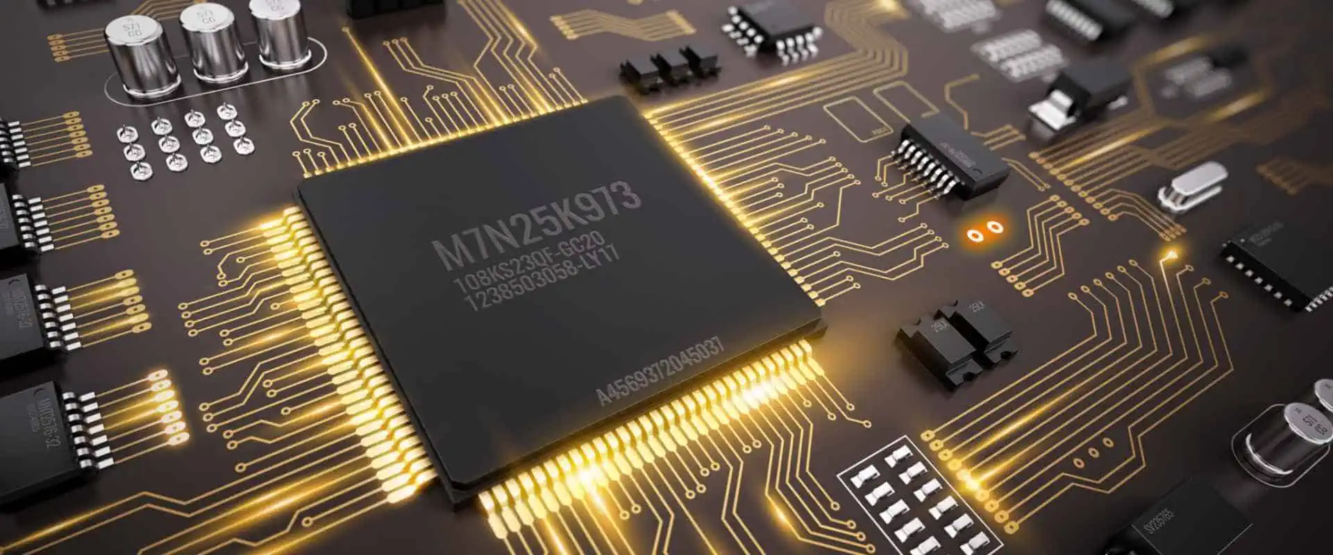
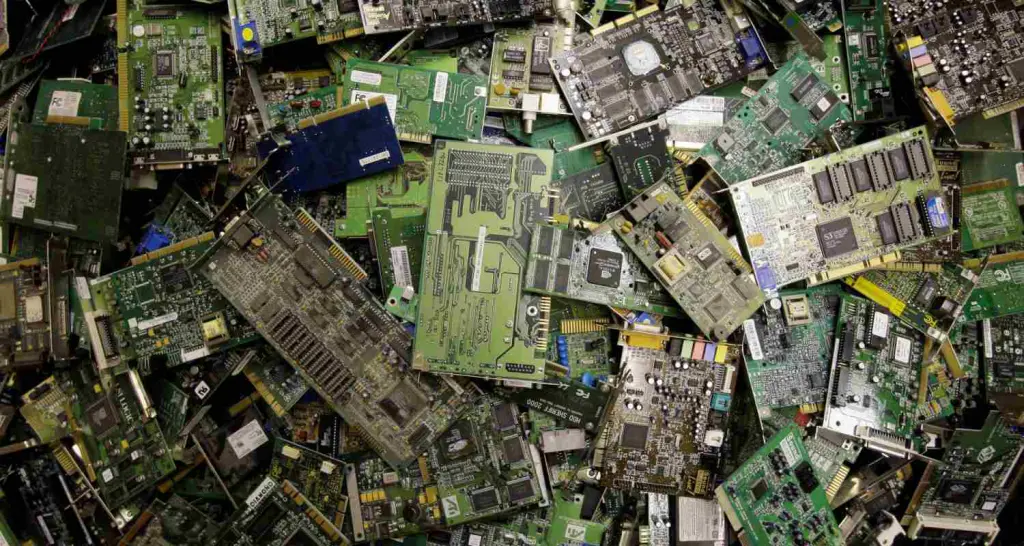
PCB Depaneling, also referred to as singulation, is the process of separating printed circuit board (PCB) assemblies from large fabricated panels into individual PCB units.

This article provides a comprehensive overview of conventional manual and automated laser-based PCB depaneling approaches. Key aspects covered include:

  • Need for panelization in PCB fabrication
  • Manual depaneling tools and techniques
  • Overview of laser depaneling/singulation
  • Working mechanism of laser systems
  • Laser parameters and considerations
  • Quality comparison between methods
  • Advantages of laser depaneling
YouTube video

Why Panelize PCBs During Fabrication?

How to Panelize in AlTIum Designer

As PCB technology evolved towards reduced feature sizes and tighter tolerances, handling of individual PCBs through fabrication steps became highly impractical and yield-unfriendly.

Panelization techniques were adopted where instead of processing single boards, multiple circuits are arranged in a large panel format and taken through fabrication flow as a whole:

  • Enables batch processing for improved throughput and yield
  • Easier handling of small circuits
  • Common tooling and nests for uniformity
  • Compatible with standard equipment
  • Panel stiffeners prevent warpage
  • Cost-effective by distributing fixed costs

After completion of all board fabrication and assembly operations as a panel, it then enters the depaneling stage.

Read more about:

Need for Depaneling Before End Use

Although PCBs are fabricated and assembled in panel formats, they need to be separated down into individual boards before final integration and end-use by customers. This is carried out through the depaneling or singulation process.

Why Depanel PCBs?

  • Panels sizes incompatible with target enclosures
  • Enable handling of PCBs during QA/testing
  • Different board formats on same panel
  • Route signals between separated boards
  • Mounting provisions require board clearance
  • Allow unit-level repair/rework
  • Accommodate contour dimensions

Thus, depaneling is an indispensable step to retrieve standalone functional boards from panels.

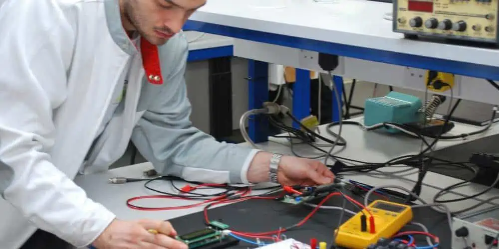
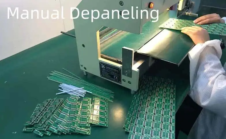
Manual Depaneling Methods

Before the advent of automated PCB singulation equipment, depaneling was performed using manual tools and procedures. These approaches are still relevant for low volume or prototype assembly pcb runs where automation is uneconomical.

Typical Manual Depaneling Techniques:

  1. Scoring and Snapping
  2. Shearing/Punching
  3. Routing
  4. Cutting with High-Speed Blade

Scoring and Snapping

This involves selectively engraving lines on the panel surface along intended breakout regions using a scoring tool. The residual web is then flexed manually to snap boards apart.

Advantages

  • Simple process without investment
  • No adhesion issues versus boards

Limitations

  • High tear rates with brittle, thin boards
  • Incapable of precision cuts
  • Large panel flexing difficulties
  • High labor involvement

Shearing/Punching

Deploys mechanical dies which impact the board with pressure sufficient to shear through board thickness when panels are loaded between top and bottom tools.

Benefits

  • Handles PCBs with components mounted
  • No debris generation risks

Shortcomings

  • Limited positioning accuracy
  • High tooling maintenance
  • Slow process speed per station
  • Risk of board flexure damage

Routing

pcb-cnc-router

Involves programmed drilling machines with routing/milling bits to cut required depaneling profiles through panel thickness.

Advantages

  • Handles close conductor spacings
  • No extensive tooling upkeep
  • Decent dimensional precision

Disadvantages

  • Unable to resolve dense board escapes
  • Generates cutting debris
  • Slow process throughput

Cutting with High-Speed Blade

Uses table-top presses with provision to mount high RPM rotary blades operated manually. Panels are pressed down during blades movement across boards for shearing action.

Pros

  • High speeds with no drilling drips
  • No plastic deformation versus boards
  • Room temperature operation

Cons

  • Limited positioning accuracy
  • Generates debris and dust
  • Risk of conductor nicking
  • High blade wear and maintenance

While suitable for small quantities, manual methods compromise production rate, precision, quality consistency and yield. They also rely extensively on operator skills.

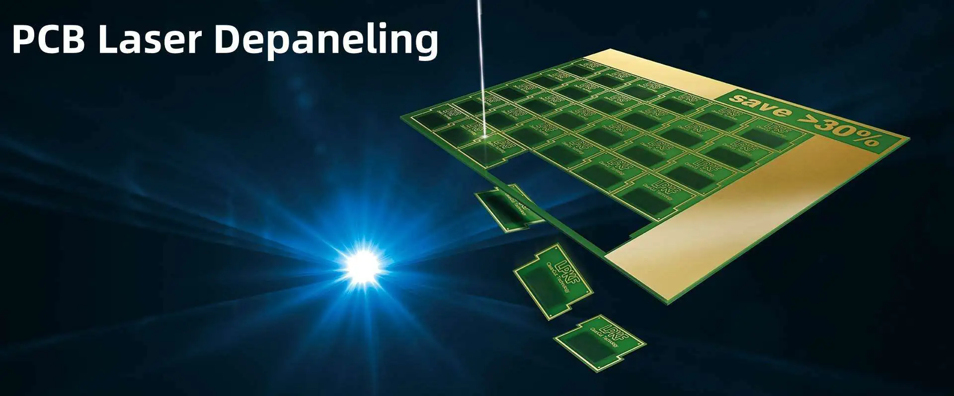
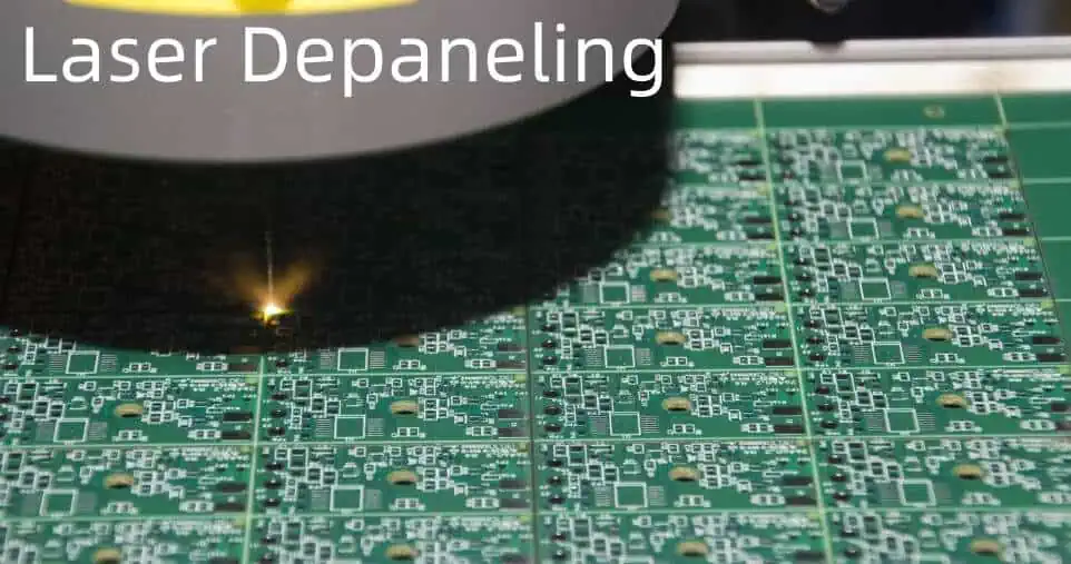
Overview of Laser Depaneling

YouTube video

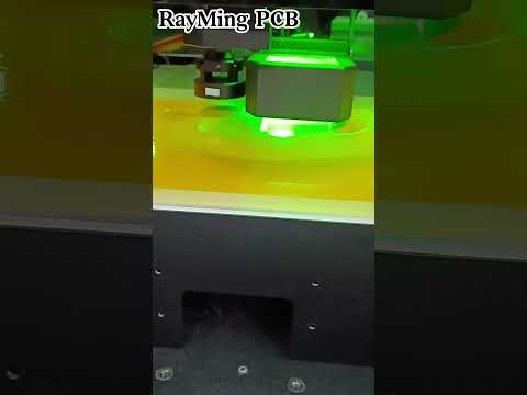
Laser depaneling involves scanning focused laser over lines corresponding to required cut paths for pyrolytical ablation of board materials. The intense laser heat vaporizes polymers, ceramics and composites to singulate boards.

It constitutes a major technological advancement versus manual means by offering:

Benefits of Laser Singulation

  • Minimal kerf widths down to ~25ฮผm
  • No mechanical contact or tool wear
  • High positioning accuracy (~25ฮผm)
  • Excellent cut quality with no micro-cracks
  • Easy depth control without exit burrs
  • Fine pitch compatibility (~100ฮผm)
  • No board flexure or dust generation
  • Automated, programmable process
  • Handling Heat-sensitive boards with components

Thus, lasers present a versatile, non-contact singulation technique. Both UV (355nm) and CO2 (10.6ฮผm) laser configurations are popular for PCB depaneling.

Laser Depaneling Methods

There are two techniques for laser-based PCB singulation:

Scribing:

Laser is used to cut specific dashed lines or patterns along the depanel regions. It creates deep grooves without going fully through the panel thickness. The boards are later snapped apart manually or using a breaking fixture.

Advantages:

  • Fast process and low power consumption
  • No complicated dust/debris extraction

Limitations:

  • Limited thickness scribing capability
  • Risk of conductor exposure or tear
  • Extra post-processing steps needed

Full/Blind Depth Cutting:

The laser completely cuts through the full board thickness to achieve complete isolation of boards in a single pass. Most common depaneling technique.

Can further be implemented through:

  • Sequential Processing: Board is moved relative to stationary laser for tracing separation path.
  • Simultaneous Full Cut: Panel traversed under large beam emitting array of laser diodes cutting all dicing streets concurrently.

Among laser techniques, sequential full-depth cutting technique offers optimal quality, precision and capability to handle high board thicknesses.

Working Principle of Laser Depaneling

Key laser ablation mechanisms:

  • Laser beam is focused on substrate through optics
  • Board material absorb photon energy inducing molecular bond breakup
  • Resultant violent vaporization causes clean material removal
  • Inert gas (N2) assists blowing away ejected particles
  • Multiple passes create cuts through full thickness

Process parameters like average power, frequency, scanning speed govern cut quality characteristics. Computerized G-code programming controls laser firing to trace complex 2D profiles.

Laser Parameters and Considerations

To achieve robust depaneling performance, appropriate laser settings need to be deployed based on board stackup.

Laser Wavelength and Type

Shorter UV wavelengths offer higher resolution but get absorbed easily requiring moisture-free boards. Longer CO2 wavelengths penetrate deeper with lower resolution. Both produce excellent cut quality without heat damage.

Pulse Repetition Frequency

Influences average laser power output. Typical range 100 Hz to 80 KHz. Lower frequencies limit material heating but reduce throughput.

Pulse Width / Duty Cycle

Proportion of laser on-time per cycle governing pulse peak power. Lower duty cycles prevent overburning. Range of 10-100 nS common.

Beam Quality Factor

Defined as laser beam diameter-to-divergence ratio indicating beam sharpness. Higher >0.8 preferred for smaller spot sizes and smooth kerf walls.

Cut Speed

Laser systems support programmable scanning velocities from 10 to 1000mm/s. Faster the cut speed lower the heat exposure for adjacent areas.

Gas Pressure

Process gas pressure between 0.5 to 6 bar helps evacuate melt on time preventing re-deposition.

Quality Comparison of Methods

Depaneling Quality Characteristics

ParameterManualLaser
Cut Accuracies+/- 0.2mm+/- 0.025mm
Width/Channel Compatibility>2mm>0.1mm
Debris GenerationHighNone
Conductor Damage RiskHighNone
Process ControlLowExcellent
Automation ScopeMinimalHigh
Throughput SpeedSlowVery high

Lasers match closest to the accuracy, precision and quality demands of current-age PCBs designs containing shrinking features and tight clearances while minimizing damage risks.

Advantages of Laser Depaneling

Benefits of Laser Depaneling Systems

  • Extremely narrow cut widths with fine control
  • Permit very close proximities to conductors
  • Clean, dross-free cuts without cracks
  • No mechanical stresses or board handling
  • High depth resolution without exit burrs
  • Excellent precision and repeatability
  • Environment-friendly process
  • Minimal heat induction in materials
  • Works reliably across panel sizes

These characteristics make laser depaneling the technology of choice for next-generation PCB singulation and dicing applications.

FAQs

Can components remain populated during laser depaneling?

Yes, most laser singulation systems permit cutting around components without causing damage. Unique galvo-split optic technology allows navigating around parts and connectors.

What safety measures are essential for laser systems?

Critical precautions involve proper public safety cage around equipment, fail-safe galvo motor controls, dual interlock switches, emission indicators and correctly rated optics among other aspects.

Does laser cutting leave behind harmful fumes?

Laser ablation generates only negligible smoke limited to the kerf width. Extractor systems filter out minute particulate matter to prevent operator exposure. No chemical effluents involved.

Can stress relief be incorporated during depaneling?

Laser systems support adding โ€œmouse bitesโ€ or tabs structures at dicing streets which act as stress relieving features preventing pad lift off or solder joint damage.

Is laser cutting technology expensive to adopt?

Although high initial capital investment is required, lasers offer strong ROI through process speed, quality and yield over other alternative approaches to PCB singulation. Operating costs are also minimal without expendables.

25+ Best PCB Design Courses and Certifications for Beginners ( 2023 Updated with Cost)

Printed circuit board (PCB) design is an exciting career integrating cutting-edge hardware technologies and software tools to implement next-generation electronics. As products continue getting smarter and more connected, demand for capable PCB designers keeps rising.

However, learning PCB layout software and design principles on your own can be challenging. Quality courses efficiently build beginner competencies through structured curriculums and practical projects.

This guide compares over 25 different PCB design classes and certification programs from online platforms like Udemy to dedicated training centers. Whether wanting to reskill into electronics design roles or advance existing embedded hardware careers, these educational resources provide ideal launch points.

Best Online PCB Design Courses

Online platforms allow accessing beginner-friendly PCB design courses from home on flexible schedules. While lacking equipment for physical board fabrication, these classes offer strong foundations in EDA software and PCB layout fundamentals through pre-recorded content.

Udemy

With over 213,000 students enrolled to date, Udemy offers popular on-demand video courses teaching Altium Designer and other EDA tools.

Key Courses

CourseInstructorDurationRatingPrice
Complete Electronics Design using Altium DesignerReshmiSK23.5 hours4.4 โ˜… (772)$99.99
The Complete PCB Design Course Using Altium DesignerSyed Noman Hanif10.5 hours4.4 โ˜… (154)$94.99
PCB Design for ManufactureChris Gammell1.5 hours4.2 โ˜… (51)$19.99

Udemy classes let you learn at your own pace for one-time fee. Their highly-rated curriculums designed by industry experts build strong proficiency in tools like Altium Designer through detailed explanations plus downloadable project files to follow along. Monthly subscriptions around $30 also enable unlimited course access.

Key Strengths

  • Top-rated classes with thousands of reviews
  • Project-based learning using actual tools
  • Flexible on-demand video format
  • Frequent discounts up to 90% off

Considerations

  • Self-directed learning without direct instructor access
  • Limited hardware design/build opportunities
  • Skill application still requires portfolio projects

Pluralsight

As another online learning platform, Pluralsight offers extensive libraries of PCB design and EDA software video courses from authors like Rusty Armstead.

Example Courses

Introduction to Altium Designer
Printed Circuit Board Design Using Altium Designer
Creating Manufacturable Designs with Altium and OrCAD

Structured curriculums systematically build PCB layout expertise leveraging quizzes, coding challenges, supplemental resources and progress tracking. Access requires monthly ($45) or annual ($495) subscriptions.

Key Strengths

  • Taught by practicing engineering leaders
  • Engaging teaching formats
  • Alignment to relevant job skills

Considerations

  • Subscription cost
  • Less hands-on than dedicated PCB EDA tools

Coursera

Programs from major universities like University of Colorado Boulder introduce PCB layout software and hardware design skills through guided projects.

For instance, their hands-on Introduction to Electronics series explores simulation tools, soldering, and measuring circuits assembled on tester boards. Self-pacing makes achieving Specializations convenient despite weekly deadlines.

Key Strengths

  • Instuctor support and graded assignments
  • Build physical validation skills
  • Accredited certifications

Considerations

  • Slower paced/less tools depth than dedicated courses
  • Pay per Specialization instead of unlimited access

LinkedIn Learning

Over 1,000+ electronics design courses are available on demand through LinkedIn Learning (formerly Lynda) for approximately $30/month. While most focus on analog circuits and programming, many modules like Altium Essential Training offer strong introductions to key PCB design tools and concepts.

Key Strengths

  • Taught by practicing engineers
  • Certificates to validate completion
  • Frequent new releases

Considerations

  • Limited advanced PCB-specific design content
  • Shorter format lacks complex projects

Udacity

Specialized Nanodegree programs from Udacity like Embedded Systems provide self-paced instruction spanning prototyping, simulation, and troubleshooting with mentor support. The project-based curriculum has students assemble and debug a microcontroller-based robot.

Key Strengths

  • Live expert project reviews
  • Certification builds resume credentials
  • Aligns content to job requirements

Considerations

  • Nanodegrees have limited PCB-focused content
  • Higher cost than single courses

On-site PCB Design Institutes

Embedded Hardware Engineer

For those able to attend intensive multi-day programs in person, dedicated training centers around the world offer extensive hands-on PCB design and fabrication instruction leveraging professional grade lab equipment.

EPTAC Corporation

EPTAC leads public, private and custom PCB design courses including 5-day bootcamps and multi-week certifications on tools like Altium, Allegro, and PADs. Their expert instructors balance lectures with individual/group project modules that cement learnings.

Key Programs

CourseDurationFormatPrice
Fundamentals of High-Speed PCB Design5 daysIn-person/Online$2,495
Allegro PCB Editor v17.25 daysIn-person/Online$2,495
Altium Designer for High-Speed5 daysIn-person/Online$2,495

In addition to classes nationwide, EPTAC offers scheduled online offeringsand private sessions at client sites. Their combination of theory and practical application accelerates PCB design skill building.

Key Strengths

  • 30+ years delivering PCB training
  • Balance of tools + design principles
  • Expert instructors with Brown University pedigree

Considerations

  • Class schedules vary by location
  • Limited hardware fabrication

PCB Design LAB

This German technical training institute focuses exclusively on electronics design instruction including week-long PCB workshops. Attendees gain intensive hands-on experience under expert guidance fabricating actual boards to cement concepts.

Sample Workshops

CourseDurationFormatPrice
Professional PCB Design with EAGLE5 daysIn-personโ‚ฌ1,625
Professional PCB Design with Altium5 daysIn-personโ‚ฌ1,625
Embedded Systems Programming5 daysIn-personโ‚ฌ1,625

These immersive programs rapidly accelerate practical board design and development competencies. Small class sizes ensure personalized attention troubleshooting challenges during projects.

Key Strengths

  • Specialized pure technical training
  • Create boards start to finish
  • Build portfolio pieces

Considerations

  • Limited schedule offerings
  • Outside US-based location

Synopsys DesignWare Technical Training

Covering tools from Synopsys like SaberRDDRN, HSPICEยฎ, and CodeLink this dedicated curriculum develops skills for simulation, analysis and PCB design specialties like DDR interfaces. Custom private courses also available.

Curriculum Sample

CourseDurationFormatPrice
Simulation with SaberRDDRN4 daysIn-person$1,850
Hspice/FineSim Circuit Simulation5 daysIn-person$1,995
Introduction to DesignWare IP for PCB Design2 daysOnline$995

Their globally recognized certifications confirm expertise across Synopsysโ€™ Electronic Design Automation (EDA) tool suite critical for PCB design roles.

Key Strengths

  • Aligned to industry standard EDA tools
  • Certificates from EDA leader
  • Specialized niche skill development

Considerations

  • Narrower curriculum focus
  • Limited public schedule

University PCB Design Programs

PCB Programmer Debugger

Formal engineering degrees offer the most comprehensive foundation combining extended curriculums spanning electronics principles, simulation, and PCB CAD software proficiency needed for advanced roles.

BSc Electronics Engineering

A dedicated electronics engineering bachelorโ€™s degree provides rigorous grounding in topics like:

  • Embedded Systems Programming
  • Circuit Simulation and Analysis
  • IC Architecture and PCB Design
  • Signal Processing Theory

Capstone design projects have students assemble functioning boards addressing real-world product requirements.

Key Strengths

  • Complete skillset spanning hardware and software applied through complex projects
  • Recognized Engineering qualification

Considerations

  • 4-year full-time commitment
  • High tuition costs

Vocational IT Qualifications

Specialize official competencies through shorter technology-focused qualifications like:

BTEC Level 3 Diploma Engineering – Electronics

Key Details

DurationAssessmentsLevel
1-2 YearsAssignments + ExamsA-Levels / AP Exams

Topics encompass analog/digital electronics, PCB layout/manufacturing methods, embedded systems, and project design/testing processrigor.

Key Strengths

  • Formal certification of specific skills
  • Aligns content directly to job functions

Considerations

  • Less generalized than university Engineering degrees
  • Still 1-2 year endeavour

Getting Recognized Credentials

Certifications confirm attainment of industry-defined PCB design standards. While voluntary, they signal commitment to stay updated on latest tools/regulations.

EPTAC Certified IPC Specialist Programs

Key Credentials

AreaExam Code
IPC-A-600 PCB AcceptabilityCIS-110
IPC-A-610 PCB Assembly AcceptabilityCIS 150
IPC J-STD-001 PCB Soldering CompetencyCIS 205

Dramatically boost employability passing one or more niche assessments offered through authorized centers worldwide like EPTAC.

Benefits

  • Confirms specialized capabilities beyond just software self-learning
  • Differentiates commitment to quality
  • Often required at larger corporations

Preparation Needed

  • Study materials span hundreds of pages per test
  • Many still only pass final exams after taking aligned courses

Altium Certified Designer

Formalize Altium expertise through their globally recognized certification program available at Associate, Professional, and Expert progression levels. Testing occurs at PearsonVUE test centers.

Key Details

  • Self-study learning materials provided
  • Online practice exam identifies weak points
  • 90 minute 50 question final test

Attaining ADC status signals competence both capturing complex designs and applying best practices.

Benefits

  • Confirms real-world proficiency vs just tool tutorials
  • Continuous skill benchmarking path
  • Highlights dedication attracting job opportunities

Preparation Needed

  • Months of hands-on experience before attempting
  • Expect questions spanning hundreds of features

Keeping Skills Current

Hardware Testing
Hardware Testing

The fast pace of progress in PCB design requires ongoing education every few years as tools and regulations advance.

Approaches to Consider

  • Attend 1-2 day conferences like PCB West covering latest technology
  • Take new Altium/Allegro/OrCAD courses on revised versions
  • Refresh key standards knowledge like IPC-2221Design before seeking updated certifications
  • Signup for monthly design industry newsletters highlighting changes

Staying current is critical as expectations continuously rise for what PCB designers must comprehensively understand implementing cutting edge products. Lifelong learning enables securing ideal roles.

Selecting the Optimal PCB Design Course

With so many learning options available, focus training plans based on current objectives:

PurposeRecommended Format
Switch careers to PCB designUniversity engineering degree or vocational circuit/electronics diploma qualification
Gain beginner PCB layout familiarityIntroductory Udemy or LinkedIn Learning courses
Specialize existing EE skillsDedicated tool (ex. Altium, Allegro) training through Synopsys/EPTAC
Validate knowledge depth through certificationSelf-study then sit IPC/Altium/Allegro credential exams

While unchecked online content risks perpetuating misconceptions, trusted providers with strong reputations avoid bad practices hindering real designs. Hands-on project application cements lessons.

Conclusion

This guide summarized over 25 different training resources from online platforms to university degrees suitable for efficiently developing PCB design competencies. Whether wanting to reskill into electronics hardware roles or expand existing embedded systems backgrounds, quality courses provide structured knowledge with expert support.

Match learning formats like short tool-centric bootcamps, accredited curriculums granting formal qualifications, and globally recognized certifications to current objectives. Lifelong occasional retraining enables staying abreast of relentless industry tool/standards innovation.

Investing in robust initial training combined with ongoing education throughout a career allows reliably applying evolving technologies critical for next-generation product development and sustainable employment.

FAQ

Q: Can I learn PCB design without enrolling in courses?

Self-teaching PCB layout software is possible using hobbyist licenses and online resources. However, missing critical context risks developing knowledge gaps that manifest in unusable board designs. Quality courses efficiently build competencies.

Q: How much does a PCB design course cost?

Prices vary widely from $15 online introductory modules to $5,000+ for multi-week intensive certifications. Consider investing at least $100 per major tool needed for local jobs. Subscription access enables trying libraries affordably.

Q: What software should PCB design courses teach?

Priority mastering platforms like Altium Designer, OrCAD, PADs, Allegro, and Zuken widely used at electronics companies hiring designers both locally and remotely. Once proficient in one tool, skills more easily transfer.

Q: Can I work professionally after taking a Udemy PCB course?

While quality Udemy classes build software familiarity, applying skills designing manufacturing-ready boards still requires months of practice. Pair online learning with portfolio projects. Entry-level roles may expect vocational certifications too.

Q: How long does it take to become a skilled PCB designer?

Expect at least 2-3 years growing from beginner to mastery. Take incremental courses while gaining progressive hands-on application opportunities through volunteer designs, hobbyist projects, freelancing, and formal intern roles. Experience breadth accelerates competence.

How to Become a PCB Design Freelance ? ( Tools and Skills )

Getting Started as a Freelance PCB Designer

Printed circuit board (PCB) design is an in-demand field as electronics manufacturers rely on freelancers to supplement internal teams designing boards for new products. With more companies outsourcing at least some of their PCB design needs, freelancing lets experienced layout engineers take greater control over their schedule and income.

However, successfully transitioning to full-time PCB design freelancing requires more than just technical competency. This guide covers key steps needed to establish and sustain an independent freelance business designing printed circuit boards:

Learn In-Demand PCB Design Skills

While entry-level PCB roles may involve PCB librarian responsibilities, most freelance work centers around board layout and schematic capture. So your first priority is gaining proficiency in PCB design tools like:

Altium Designer – The industry standard for PCB layout and MCAD collaboration

Cadence Allegro – Widely used at mid/large size companies

Mentor Graphics Xpedition – Particularly popular at semiconductor firms

Zuken CR-8000 – Has a strong presence in several verticals like automotive

Check job listings in your target market to identify which EDA platforms are most requested. While tool principles translate, focus initial training on commonly used PCB design environments in your region to offer immediately productive services.

Beyond software expertise, assemble a portfolio highlighting experience delivering production-ready PCB layouts, library management, DFx, signal integrity simulation and prototyping collaboration. Document your capabilities across the end-to-end design flow.

Purchase Necessary Tools and Infrastructure

Once ready to start operating as freelancer, invest in software licenses and equipment enabling delivery of professional services:

EDA Software

ItemDescriptionEst. Cost
Altium DesignerPCB/FPGA Layout + MCAD Integration$7,000/year
ANSYS SIwaveSignal Integrity Simulation$5,000/year
Multiple EDA ToolsEnsure support for client preferences$10,000+/year

Computing Hardware

ItemDescriptionEst. Cost
High Core Count Workstation16+ core CPU, 64GB+ RAM, GPU acceleration$4,000+
Large Monitors>= 32โ€ for visibility$800 ea
Fast Network ConnectionLow latency for remote access$500/year

Productivity Software

ItemDescriptionEst. Cost
Microsoft OfficeDocumentation, analysis, client comms$70/year
Video ConferencingMeetings with clientsFree – $20/month
Project ManagementTrack milestonesFree – $20/user/month

Leverage tax write-offs/depreciation to offset costs of requisite software, accessories, reference materials, and dedicated home office workspace ergonomic equipment as permissible.

Establish Freelance Business Processes

With tools in place, formalizerepeatable processes that enable delivery of quality services at scale to multiple clients:

  • Document design, analysis, review, and handoff procedures in a quality system
  • Standardize file management conventions for projects
  • Setup design templates, symbol libraries to jumpstart new designs
  • Identify preferred component datasheets/models/footprint sources
  • Check pricing and order parts for quick prototyping / evaluation
  • Develop scripts to automate repetitive EDA tasks

Refine templates and flows using version control systems like SVN or Git for change tracking. Be meticulous capturing critical project details so new engagements ramp quickly.

Build Client Portfolio

A healthy roster of ongoing client projects provides steady freelance work. Diversify your customer base across industries and PCB types to smooth volatility from individual businesses.

Marketing Activity Ideas

  • Website showcasing capabilities & past project examples
  • PCB design conferences & tradeshow attendance
  • Guest blog posts for industry websites
  • Promotion through freelance job boards
  • Search ads for relevant design keywords
  • Cold call/email small/mid-size local engineering firms

While early leads may start slowly through individual outreach efforts, as your reputation and portfolio growsrecurrent customers will transmit several new opportunities. Deliver exemplary services that make clients want to recommend you within their networks.

Operating as a PCB Design Freelancer

Managing the business aspects from acquiring customers to delivering finished boards can be quite demanding. Follow best practices to streamline operations:

Secure Design Contracts

Treat the sales process professionally using engagement letters detailing:

  • Clearly defined scope – Requirements, deliverables, and key milestones
  • Payment terms – Amount, schedule, reimbursements, late fees
  • IP ownership – Licensing/transfer specifics
  • Liability limits – Protect yourself appropriately

Do not proceed without signed approval from all stakeholders to avoid future disputes.

Maintain Organized Design Data

Stay on top of documentation, analysis, and project data using tools like:

  • Microsoft OneNote – central working notebook
  • Microsoft OneDrive – synchronize files across clients
  • Altium 365 – access design files from anywhere

Share real-time PCB views augmented with live annotations to ease remote reviews. Store prior projects on spinning disks for rapid comparable retrieval.

Communicate Proactively

Set client expectations upfront through regular status reports detailing:

  • Recent progress over past week
  • Planned tasks for next week
  • Summary of any obstacles impeding completion

Raise issues early through email/calls if priorities shift or problems emerge needing customer feedback to resolve. Be responsive addressing questions to prevent delays.

Stay Current on EDA Advancements

While mastering a specific PCB design toolset enables efficiently delivering projects, regularly refresh skills by:

  • Reading EDA release notes and evaluating new versions
  • Testing complementary analysis/simulation tools
  • Experimenting with emerging technologies like machine learning-assisted layout

Significant innovation happens between major tool revisions. Don’t let comfort with existing environments breed complacency.

Sustaining an Ongoing Freelance PCB Design Business

Maintaining a consistently booked schedule across years as freelancer requires ongoing hustle:

Maintain Visibility

Continue cultivating organic growth through:

  • Speaking at local engineering Meetups
  • Publishing tutorials / videos / webinars
  • Attending regional PCB design events
  • Contributing to online technical forums

This exposure seeds inquires from members of your broader professional community.

Explore Services Expansion

Occasionally evaluate opportunities to expand your capabilities:

  • Learn additional PCB layout tools
  • Offer design reviews based on deep expertise
  • Provide mentoring for early career designers
  • Train companies’ layout teams on complex methodologies

This diversifies income streams while leveraging hard-won talents.

Preparing for Retirement

If desiring to step away from intensive daily design project work over longer term, start gradually shifting directions through steps like:

  • Reduce client workload over multiple years
  • Refer trusted associates to take on customers as you wind down
  • Transition to advisory roles leveraging your expertise
  • Focus on creating online courses, blogs rather than delivering bespoke designs

Plan ahead to reduce shock going from active projects one day to absence the next. Customers and colleagues will appreciate continued wisdom even as design tools eventually retire too.

FAQ – PCB Design Freelancing

Q: Is freelancing riskier than traditional employment for PCB designers?

Freelancing does involve additional uncertainty from inconsistent project pipelines and responsibility for your own benefits. However, compensating higher rates over time can offset periods with fewer customers. Many find the flexibility and control over work rewarding.

Q: Can I work full-time remotely as a freelance PCB designer?

Absolutely. Remote work is common for freelancers using collaboration platforms like Altium 365 and video conferencing. Some independent designers even operate while traveling around the world!

Q: What tax implications exist when freelancing?

You are responsible for quarterly estimated income taxes, self-employment taxes, and tax documents like 1099 forms. Consider meeting with an accountant to understand write-offs and optimal corporate structures. Significant tax savings for businesses help offset the additional planning workload.

Q: Is freelancing lonelier than office jobs?

Freelancing does require more initiative developing professional connections. However, remote tools enable easy communication with collaborators. Consider co-working spaces or local networking events to prevent isolation.

Q: Can I use freelancing to transition into retirement?

Yes, freelancing supports gradually scaling down through fewer or more flexible projects. Some even shift into training or blogging roles leveraging their expertise while slowing direct design work. Plan ahead for this evolution.

Conclusion

Launching a freelance PCB layout business allows experienced designers the freedom to control their schedules and leverage specialized skills honed over past projects. While establishing steady clients takes consistent self-promotion, word of mouth referrals facilitate growth over time. Savvy independents also watch industry trends to offer complementary training or advisory services in the future.

Careful upfront planning enables smoothly operating the business aspects like contracting, taxes, tool management that support consistently delivering quality designs according to committed schedules. However, by following best practices covered here, PCB designers can thrive taking their careers in an independent direction.

15 PCB Design Interview Questions (With Example Answers)

Printed circuit board (PCB) design is an essential engineering function for developing electronic devices and components. PCB designers are highly sought-after to help create circuit boards that are compact, efficient, and robust enough for today’s complex electronics.

Companies seek experienced PCB designers who understand schematics, can effectively use PCB design software, and know how to transform electrical engineers’ functional requirements into optimized board layouts ready for fabrication. Strong communication skills are equally critical for collaborating across engineering teams and manufacturing partners.

This article summarizes commonly asked interview questions for PCB design engineers to assess hard and soft skills relevant to the role. We provide illustrative answers to the questions along with data tables on key PCB design principles that new hires should understand. An FAQ section also covers additional questions candidates have when preparing for PCB design interviews.

Technical PCB Design Interview Questions and Answers

The following are examples of role-relevant technical questions interviewers may ask related to PCB architecture, material selection, component placement, design analysis, and prototyping methods.

1. How do you ensure optimal trace routing in complex multilayer PCBs?

To optimize multilayer PCB trace routing:

  • Analyze signal return pathsย to minimize noise, EMI, and parasitic impedances
  • Maintain separationย between critical traces to prevent coupling interference
  • Balance trace lengthsย to synchronize timing-critical signals like clocks
  • Avoid 90ยฐ anglesย on traces which creates discontinuities that disrupt high-speed signals
  • Route clock/data traces orthogonallyย to isolate signals and minimize crosstalk
  • Use wider traces for powerย to handle required current capacity
  • Add shieldingย (e.g ground planes) between noisy and sensitive circuitry

Proper trace routingminimizes noise, interference, and timing issues in complex PCBs, enabling reliable performance from integrated circuits even at fast clock rates. I would also run signal integrity simulations of proposed PCB stackups using software like HyperLynx to validate trace routing before manufacturing prototypes.

2. How do you manage heat dissipation and thermal issues in PCB design?

To manage PCB thermal issues, I would:

  • Identify high-power componentsย early in the design process
  • Create local areasย on the board to mount heat-sensitive components
  • Add thermal vias/padsย under hot components to conduct heat into ground planes
  • Incorporate exposed copper planesย on outer board layers to spread and dissipate heat
  • Use PCB finishes likeย ENIG that enhance thermal transfer
  • Simulate airflowย across board with CFD software and refine enclosure/cooling approach
  • Verify temperatureย at critical components through thermal imaging of working prototypes

Considering thermal design from the beginning prevents hot spots on circuit boards that can impact device reliability and performance. I collaborate closely with mechanical engineers to optimize cooling system approaches while ensuring the electronics can withstand any vibrations or other environmental conditions.

3. How would you test a new PCB design before manufacturing a full production run?

To fully validate a new PCB design before high-volume manufacturing, I would build and test prototypes in stages:

Stage 1:

  • Perform design rule checks and useย CAM filesย for initialย prototypingย usingย PCB milling
  • Functionally test withย breakout boardsย to check each IC/component

Stage 2:

  • Manufacture ~5ย test boardsย from theย fabrication house
  • Performย bare-board testingย to validate electrical connectivity
  • Assemble boards toย validate functionalityย against schematics with basic programming

Stage 3:

  • Manufacture ~50ย pilot run boards
  • Test withย final assemblyย (processors, peripherals etc.)
  • Run boards forย extended soak testingย under environmental stress conditions

Prototyping catches design errors early, while pilot runs validate manufacturing and assembly processes. This staged testing lowers risks prior to large-scale PCB fabrication for new products. I work closely with techs and engineers during each test phase and enter issues into bug tracking tools to enable rapid design modifications.

4. How do you ensure manufacturability and DFM (design for manufacturing) in your PCB layouts?

Corne PCB Layout
Corne PCB Layout

I optimize PCB layouts for manufacturing success and yield by:

  • Leaving adequate clearance around pads/vias based on fabrication capabilities
  • Addingย fiducialsย for precise alignment during PCB assembly -Using minimum pad sizes for best soldering results and eliminating thermal relief that reduces pad size
  • Creatingย test pointsย to enable quality assurance checking during production
  • Selecting standardย thicknessesย for laminate/copper that match manufacturing inventories
  • Defining route paths between pins that allow forย chemical etching
  • Specifyingย panel sizesย that maximize board quantity per panel production run

I also communicate frequently with our fabrication partners, sending regular design updates and discussing any potential manufacturability issues I foresee in layouts. This design-for-manufacturing (DFM) approach prevents delays and unnecessary costs in Readying designs for volume production.

5. What are some best practices for spacing PCB components and traces?

Some key PCB component and trace spacing best practices include:

  • Maintainย 2-3x dielectric spacingย between traces to prevent short circuits
  • Keepย 3-5x width spacingย between high-speed or noise-sensitive traces
  • Allowย 5-10x dielectric spacingย around integral ICs (e.g. microprocessors)
  • Placeย 0402 size passives 0.1mm apart, while larger components need 0.2mm spacing
  • Ensure adequate clearance between traces and edges/holes to account for fabrication tolerance
  • Use wider gaps (up to 25x dielectric) for very high voltage traces (>100V)
  • Keep soldermask expansion modest (0.075mm) to prevent exposed copper shorting

I reference IPC standards like IPC-2221 and stay in close contact with fabrication/assembly partners regarding spacing requirements for manufacturability and reliability. Component placement software is invaluable for rapidly validating spacing rules.

6. How would you perform signal integrity analysis on a new PCB layout?

My general signal integrity analysis approach is:

  1. Identifyย critical timing paths and interfaces (e.g SPI, USB) on schematics along with theirย characteristic impedances
  2. Select PCB stackupย using impedance calculators to match transmission line properties
  3. Route tracesย for those nets with controlled widths/spacings to achieve impedance targets
  4. Model transmission linesย and attached drivers/receivers in SPICE or IBIS
  5. Simulate signal waveformsย with real world effects like cross-talk to identify reflections/ringing
  6. Re-route tracesย as needed to correct issues observed in simulations
  7. Measure eye diagrams and signal qualityย on working prototypes using oscilloscope and probing

This workflow validates all signals will have intersymbol interference below permitted thresholds despite noise from high-speed routing complexities. I pay special attention to clock distribution networks which are sensitive to reflections. Signal integrity is key for avoiding errors and timing problems in precision circuit boards.

7. What are some suitable PCB substrate/laminate materials for RF circuits designs?

Good PCB substrate materials for RF designs have consistent dielectric properties, low loss tangents, and use high resistivity laminates:

  • PTFE compositesย like Rogers RO4000 series have stable dielectric constants and low loss
  • Ceramic filled PTFE boardsย provide thermal stability for precision RF circuits
  • High frequency/speed FR4ย improved for RF performance
  • Halogen-free laminatesย like Isola Astra MT77 meet strict environmental requirements
  • Glass reinforced hydrocarbonsย offer high flexural strength for rigid-flex RF constructions

Material selection depends on balancing cost, thermal capabilities, moisture absorption, Z-axis expansion, and dielectric properties across operating bands and temperatures. I collaborate with RF engineers to model proposed stackups in electromagnetic simulators like Keysight ADS to determine if materials provide adequate isolation and controlled impedances.

8. How would you verify manufacturability constraints are met during PCB layout at companies like ours with 6 mil line/space capabilities?

To confirm my PCB layouts meet or exceed the fabrication constraints at our company such as 6 mil line/space, drill sizes and other tolerances, I would:

  • Maintainย design rulesย file specified by the manufacturer inside layout software that enforces their design constraints
  • Have our CAM team generateย gerber filesย from my board layouts
  • Submit gerbers directly to manufacturer forย design rule checkย through their portal to validate no violations
  • Work with fabrication partners onย DFM reviews earlyย during layout and modify boards based on their feedback
  • Procureย test couponsย with representative line/space traces for quality assurance
  • Visually inspect PCBsย under microscope once received to check line widths across layers

This comprehensive strategy ensures manufacturability is built into the design from the start and any capability issues get identified prior to running my layouts through production. I also stay current on process improvement roadmaps from partners to maximize exploitation of latest line resolution and via structure capabilities.

9. What advantages does using through hole vias offer compared to other interconnect options in multilayer PCBs?

Using plated through hole (PTH) vias instead of other via structures offers several advantages for multilayer PCB interconnect:

Reliability

  • Provenย robust connectionsย between layers with complete plating coverage inside holes
  • Does not require filling thusย avoids voidsย which improves thermal transfer

Process Compatibility

  • Works withย nearly all board fabricationย processes (subtractive, semi-additive, etc)
  • Enables joiningย dissimilar laminatesย since holes span all layers

Layout Flexibility

  • Can connect any layer atย angles not feasibleย with staggered/skip vias
  • Simplifies routingย since traces can jog vertically between signal layers

Cost Savings

  • Lower drilling costsย compared to using multiple blind/buried vias
  • Reduce lamination costs when thicker dielectrics not required for other via approaches

For these reasons, many high reliability or cost-optimized PCB designs still leverage PTH vias for optimal connectivity despite continuing advances in blind/buried via fabrication capabilities.

10. How would you design impedance matched traces to interface with a 25 Gbps NRZ serializer IC in a complex PCB stackup?

jlcpcb impedance control

Here is my approach to routing 25Gbps single-ended traces matched to serializer ICs:

  1. Obtainย target differential impedanceย from IC datasheet, usually aroundย 100 ฮฉ
  2. Useย Saturn PCB toolkitย to calculate widths/spacings in our board stackup to achieve impedance
  3. Define matched traceย design rulesย (e.g. 6 mil width / 11 mil spacing to layer 2 refernce)
  4. Ensure traces have >=ย 50 mil separationย from other nets to minimize interference impact
  5. Model transmission lines in HyperLynx and simulate with IBIS models to verify impedance tolerance across insertion loss peak
  6. Implement matchedย length tuningย using meandered geometry if simulations show significant impedance deviations
  7. Focus on symmetrical routingย of the differential pair to provide consistent propagation delay

Close collaboration with signal integrity engineers at each step validates simulations match measured results from working prototypes. Impedance control is critical to allow multi-gigabit serializer ICs to perform reliably.

11. How can you prevent field failures related to electromagnetic interference (EMI) in complex PCBs?

To prevent issues from electromagnetic interference in complex circuit boards, I would employ shielding, component placement/routing approaches that reduce unwanted emissions at key harmonics:

  • Use aย continuous ground planeย to provide low impedance return paths
  • Place potential noise sources (processors, crystals, inductors etc) distant from sensitive analog inputs
  • Enclose radiating ICs in isolatedย compartments/cagesย connected to ground planes
  • Designย cutouts in planesย that form filters blocking emission around critical traces
  • Specify ferrite beads, bypass capacitors, and otherย filtering components
  • Validate EMI emission spectrum against regulatory limits by testing prototypes in RF chambers

By dedicating sufficient layout real estate for isolation and control of radiated/conducted interference, I can prevent external noise disrupting inner layer signals in densely packed PCBs operating in noisy environments. Proper EMI management is mandatory for devices like medical equipment with life-critical functions.

12. How do you ensure SPICE circuit simulations correlate accurately to measured data from physical PCB prototype builds?

To accurately correlate PCB simulations to measured data, I work methodically through the following areas to build confidence that simulated behavior mimicks real world performance within acceptable tolerances:

Model Accuracy

  • Verifyย component modelsย used match manufacturer spice/IBIS models for each device’s package/pins/parasitics
  • Define boards power architecture from schematics and validate rail sequencing/voltage thresholds

Test Correlation

  • Ensure properย test conditionsย set in spice align to physical hardware test setup
  • Correlate results from simulations ‘best case‘ ‘worst case‘ and ‘nominal voltage‘ conditions

Parametric Sweeping

  • Run monte carlo simulations sweeping values of critical passives, trace impedances etc through realistic tolerance ranges
  • Confirm measured data falls within expectation bands of sweep analysis

Design Iterations

  • Tweak component values and routing based on correlation findings
  • Progressively reduce differences between simulated estimates and measured characteristics

Through careful, iterative verification of simulation settings and assumptions against real hardware, I can reliably use simulations to predict performance issues and hunt down root causes when prototypes exhibit issues not observed in initial desktop analyses.

13. How would you measure timing delays between key signals during prototype bring-up to validate schematic specifications?

My approach to validate PCB signal timing against schematic requirements would be:

  1. Identify critical paths like clock distribution, chip selects, resets withย timing budgetsย defined
  2. Probe waveforms usingย >1 GHz bandwidth oscilloscopeย with active probes to minimize loading
  3. Use marker measurements toย quantify timing delaysย between waveform transitions
  4. Compare measured intervals toย datasheet hold/setup timesย and schematic jitter allocations
  5. Capture timing violation windows by deliberatelyย altering clock delays
  6. Adjust componentsย like series terminations to shape waveforms if measurements fall outside of permitted jitter error bands per protocol specifications

I would capture debug data across operating voltage, current consumption and temperature extremes to validate robust timing margins sufficient for unrelenting part variability and environmental stress over lifelong product operation.

14. How does transmission line theory relate to PCB design? Why is managing transmission line effects important?

Transmission line theory describes how electrical signals propagate along conductors in PCBs. Understanding these effects is key for trace routing in high speed designs:

  • Traces over ~1/10 wavelength of signal frequencies act asย transmission lines
  • Signals exhibitย reflected noise, ringning if trace impedances mismatched to source/load
  • Eye diagramsย show intersymbol interference caused by dispersion/reflections
  • Terminationsย like series resistors reduce reflections but add jitter
  • Carefulย impedance controlย through trace geometry matching and Reference planes manages transmission line effects

If uncontrolled, transmission line behaviors introduce data errors, electromagnetic interference and prevent reliable performance as data rates rise into the Gbps range. Through precise modeling and layout techniques, I can satisfy impedance targets to ensure clean signal transfer between ICs even with today’s fast edge rates.

15. How could 3D printing be used when developing new PCB boards?

2.4 ghz pcb antenna design

3D printing has a few applications that could help accelerate PCB prototyping:

  • 3D printย plastic board shapesย for trial fitting enclosures
  • Print customย jig bracketsย tailored to hold PCBs during assembly
  • Create specialย test clipsย that easily interface test gear to boards under test
  • Rapidly iterateย non-conductive standoffย shapes that securely mount boards
  • Fabricate initial runs ofย low-temperature co-fired ceramic substratesย via print processes before final LTCC production
  • Help visualize board layouts through printingย 3D modelsย highlighting component placement

While print quality is generally inadequate for conductive metallic traces on production boards, innovators continually extend 3D printing into more electronics fabrication use cases. As resolution, conductive fill materials and printable dielectric polymers improve, the technology promises toaid PCB designers refine mechanical integration even while boards themselves must use conventional subtractive/additive fabrication means for production runs.

General PCB Design Interview Questions

In addition to testing technical competencies, hiring managers often evaluate a candidate’s soft skills and cultural fit during interviews through open-ended questions like these examples:

1. Describe a case where you successfully delivered a complex PCB project with tight timelines. What challenges did you face and how did you overcome roadblocks?

Early in my career at Glorytech, we won a contract supplying motor controller boards for a major electric vehicle program with an extremely aggressive 4-month deadline from project award to delivering prototypes for design verification.

While our team was excited, I voiced concerns in our planning sessions regarding the schedule risk given several new complex features we aimed to implement that stretched our previous PCB capabilities. Rather than dilute our compelling technical proposal, the engineering lead and I rallied the team to brainstorm parallel paths we could pursue and distributed additional upfront simulation/analysis tasks to derisk elements identified on the critical path.

Leveraging lessons learned from prior projects, I optimized component placement for thermal performance and manufacturing efficiency while also

Tips for Choosing The Best PCB Design Services ( Cost, Payment Plan, Prototyping)

design for manufacturing

Choosing a reliable PCB design partner is crucial for building innovative electronic hardware products across consumer, industrial and medical segments. The expertise transforms electronic circuit schematics into manufacturable printed circuit board (PCB) layouts ready for component integration and system assembly.

This guide shares tips for smartly selecting PCB design service vendors based on critical aspects like cost models, prototyping capacities and overall technology compatibility.

Contents:

  • PCB Design Expertise Evaluation
  • Cost Models Comparison
  • Payment Plans Analysis
  • Prototyping board Capabilities
  • Ensuring Design Eco-system Fit
  • Other Considerations
  • Conclusion

Evaluating PCB Design Expertise

Foremost, assess the vendorโ€™s technical capabilities aligned to your applications through parameters like:

Skill Domains โ€“ High speed digital, analog/RF, power electronics

Tools Proficiency โ€“ Altium, Cadence Allegro, Mentor Xpedition etc.

Industry Experience โ€“ Consumer wearables, telecom systems, medical devices etc.

Complex Project Exposure โ€“ Multi-layer HDI PCBs, Flex-rigid boards etc.

Regulatory Compliances โ€“ Medical, defense standards certifications

Miniaturization Skills โ€“ Crucial for wearable and mobility applications

Library Depth โ€“ Comprehensive component library sporadic to your bill of materials accelerates design reuse

Evaluate design samples, client testimonials and capability decks during the partner selection process. Credible vendors proactively demonstrate expertise levels required for program success.

Comparing Cost Models

Broadly, PCB design services follow:

Hourly Based Pricing โ€“ Complex or iterative projects

Fixed Bid Project Pricing โ€“ Clear requirements with minimal change orders

Monthly Retainers โ€“ Long term partnerships focusing continuous design improvements

Risk-Reward Model โ€“ Shared risk for startups compensated through equity

Compare appropriate models against typical order sizes, variability, lifecycles and product roadmap visibility to identify optimal payment structures.

We next assess popular payment plans provided.

Payment Plans Analysis

2.4 ghz pcb antenna design

Design services offer flexible payment options to ease cash flows for startups and enterprises alike:

Progressive Milestones โ€“ Break down large programs into smaller milestone based payouts. Unlocks working capital while allowing better project visibility.

Bridge Financing Services โ€“ Design partners align third party financing backing prototype build costs through lending partners. Enables access to capital for enterprises pending product sales receivables.

Extended Terms โ€“ Larger vendors provide 30-60-90 days payment terms for repeat large customers. though this may cost a slight premium. Smaller firms stay limited to 30 days payment maximum.

Online Escrows โ€“ Specialized design marketplaces enable securing initial payments which are released to the vendor upon satisfaction of promised deliverables thereby reducing risk for enterprise buyers.

Evaluate if payment norms align to company financial protocols and product development budgets adequately.

Assessing Prototyping Abilities

Ideally, design partners should provide concurrent rapid prototyping facilities enabling:

Faster Design Validation โ€“ Prototypes serve proving ground for layouts ahead of final test runs

Quicker Design Revisions โ€“ Hands-on provides intuitive feedback to modify layouts, placement or thermal performance

Smooth Manufacturing Transition โ€“ Consistent build partner aligns quality standards between prototype and production

Lower Minimum Order Quantities โ€“ Enables lower volume batches for field trials

Simpler Data Packages โ€“ Single window data directly transfers from design to prototyping stage

Having synchronized prototyping capacities avoids delays between design finalization and testing product boards.

Ensuring Design Ecosystem Fit

Confirm the design tool stack integrates smoothly across your broader product realization ecosystem spanning simulation, analysis, mechanical integration, manufacturing and sustenance.

Data exchange ease across platforms like Xpedition, Solidworks, Ansys or Altium verifies optimized ecosystem fit assuring automation ability.

We finally highlight additional evaluation parameters.

Other Selection Considerations

Specializations Fit โ€“ Domain capabilities match technology roadmap

Scalability โ€“ Handle design load fluctuations

Communication โ€“ Interaction modes fit org structure

Security โ€“ Robust IP protection protocols

Geography โ€“ Time zone alignment enables collaboration

Reviews Cadence โ€“ Fits product iteration cycles

Team Retention โ€“ Lesser attrition ensures continuity

Cultural Sync โ€“ Working styles match for harmony

Balancing technical competencies along process maturity parameters upholds long term customer relationships.

Conclusion

Evaluating PCB solution partners across cost models, payments norms, prototyping synchronization and overall ecosystem integration ensures enterprise grade readiness for shortening product development cycles across cutting edge connected devices. Leverage the guidelines outlined here for smart partner selection.

Please share feedback or suggestions on enhancing this article!

How Much Does PCB Design Cost Per Hour?

Hardware Layout

Printed circuit board (PCB) design forms the core foundation transforming electronic product concepts into functioning hardware. However, specialized skills and experience are vital to expertly design the critical interconnections enabling complex circuitry operations.

This article provides an approximate per hour cost analysis for utilizing professional PCB design services either in-house or through hired contractors.

Contents:

  • Cost Influencing Factors
  • Hourly Rate Estimates
    • Entry Level Designers
    • Medium Level Designers
    • Senior Designers
    • Subject Matter Experts
  • Ways To Reduce Design Costs
  • Is Outsourcing Worth It?
  • Conclusion

Key Factors Influencing PCB Design Rates Per Hour

Several parameters impact how much organizations spend on on-demand PCB design activities:

Designer Expertise โ€“ Costs rise for niche high-speed, RF, thermal specializations

Design Complexity โ€“ High-density PCBs with tighter tolerances are pricier

Production Volumes โ€“ Higher quantities dictate more validation tests

Timelines โ€“ Rush orders or quick-turnaround accrue premium fees

Tools and IP โ€“ Specialized CAD software, license costs apply

Geography โ€“ North America and Europe have higher hourly charges over Asia

Let’s analyze approximate per hour PCB design costs across different skill levels.

Hourly Rate Estimates

Entry Level Designers โ€“ $25 to $45 per hour

Fresh graduates offer cost-efficient design services for simple, low-volume PCB applications, reference layouts etc. Firms across hardware startups and smaller product companies utilize junior talent.

Medium Level Designers โ€“ $45 to $70 per hour

Engineers with over 3 years experience adept in daily design activities such as schematics capture, placement, routing and library management. They handle moderate complexity levels for IoT devices, industrial equipment, consumer electronics etc.

Senior Designers โ€“ $70 to $150 per hour

Veterans with 8+ years experience manage intricate high-speed digital, RF and flex PCB projects. Skilled in signal integrity; thermal analysis and DFM practices. Well suited for medical, aerospace, automotive, communications systems.

Subject Matter Experts โ€“ $125 to $250+ per hour

World-class specialists with 15+ years expertise serve cutting edge organisations in silicon engineering, automotive chips, defense systems etc. Handle advanced processes like 2.5D interposers; 10+ layer high density PCBs.

Note that the above rates card is a broad benchmark. Actual pricing depends on designer background, company size and order complexity among other parameters. Geographic factors also drive some cost variance.

Now let’s explore options to reduce design overheads followed by studying the outsourcing decision economically.

Ways to Reduce Design Costs

esp32 pcb design
esp32 pcb design

Here are effective ways organizations can lower program spending on PCB design activities:

Standardize Design Templates โ€“ Enforce template re-use with predefined specs suitable for 80% projects based on technology domains like digital logic, analog sensing or power electronics PCBs. Limiting custom tools for niche applications curtails cost.

Resource Pooling โ€“ Train internal cross-functional teams across mechanical, test and systems roles on design tools. Enable groups to handle basic layout reviews, documentation and drawing updates to ease designer bandwidth.

Design Reuse โ€“ Maintain existing layouts, footprints and symbol libraries to repurpose across quick new product iterations. Further cost savings apply through panelization i.e aligning PCB sizes for optimal material utilization across each panel.

Digitize Workflows โ€“ Automate repetitive design rule checks through coding scripts rather than manual verification. Similarly standardizing analysis metrics using digital dashboards cuts down manual collation.

Offshore Captives โ€“ Expand teams through offshoringdesign captive centers in regions with lower resource wages. However, this necessitates strong IP practices.

While tight control on budgets is necessary, compromising design quality could risk product failures outweighing temporary savings. We next assess the value of outsourcing services.

Is Outsourcing PCB Design Worth It?

PCB Antenna Design
PCB Antenna Design

Organizations lacking specialized layout engineers or facing peak project loads tend to utilize external design consultants or contract engineering service partners. Does outsourcing PCB design provide real ROI against managing local teams? Let’s evaluate scenarios where outsourcing adds value:

Variable Cost Model โ€“ Efficiently scale-up or down based on design cycles rather than fixed employee costs

Niche Expertise Access โ€“ Get proficiency in complex RF, FPGA, Flex-Rigid layouts

Proximity to Supply Chain โ€“ Language/logistics alignment with PCB manufacturing regions in Asia

Accelerated Time-to-Market โ€“ Parallel multisite work drives faster turnaround

Design Innovation โ€“ External viewpoints identify creative miniaturization options

However, outsourcing has caveats around overheads of communicating elaborate requirements to outside parties. Analyze expected order volumes and product longevity scenarios along target cost structures while making the offshore decision.

Conclusion

In summary, PCB design services cost between $25 to $250 per hour relying on various factors like complexity levels, expertise required and order volumes along with timelines. While outsourcing provides access to niche resources, building some internal capabilities helps balance costs and quality for the long run.

I hope this guide offers a broad framework to estimate budgets required towards PCB design activities either through internal teams or external partners. Please share feedback/thoughts to improve the analysis!

What is the salary of PCB designer in USA ? (2023 Updated)

Human:
I’d like you to write an article using the following instructions:
Title:What is the salary of PCB designer in USA ? (2023 Updated)
Keyword:pcb designer salary
Article length: more than 5000 words
You should definitely use markdown language when creating headings, i.e. the main title should be h1 and keyword rich subheadings should be h2, h3, h4.
create appropriate tables based on the context to visualize the data for the reader.
include writing the FQA part of the article (No more than 5 questions and answers).
Assistant:

Printed circuit board (PCB) designers play a critical role in engineering electronic hardware products across consumer electronics, automotive systems, medical devices, aerospace, telecom infrastructure and more. But what salary can an experienced PCB design engineer expect to earn in United States?

This article analyzes the standard PCB designer salary ranges in USA across junior and senior levels. We examine the influencing factors driving compensation levels and top paying industries.

Contents:

  • Average Salary of PCB Designers
  • Salary Range Based on Experience
  • Industries With Top Paying Jobs
  • Factors Affecting Salaries
  • Job Outlook for PCB Designers
  • Conclusion

Average Salary of PCB Designers in USA

As per latest salary surveys and job listings analytics, the average annual pay for a PCB Designer in USA is estimated to be $73,000 as of Q1 2023.

However, salaries can span anywhere between $55,000 to $130,000 based on expertise, industry, company size and region. The visual below depicts this overall range:

Next, we analyze the standard salary brackets aligned to professional experience levels.

Salary Range Based on Experience

Entry Level (0-2 years): $55,000 to $68,000

New graduates or junior designers with below 2 years experience get average starting salaries around $62,500 annually. Interns can expect to earn $15-$25 per hour based on academic courses and skills acquisition.

Mid-Level (2-5 years): $68,000 to $83,000

With 2-5 years substantial work exposure, compensation for PCB designers typically reaches $75,500 per annum on average. Independent contracting rates also hover within the same range.

Senior Level (5-10 years): $83,000 to $130,000

Veterans with over 5 years niche experience can negotiate salaries up to $100,000 or even exceed six figures with technical specializations, domain expertise and leadership roles. Freelancing charges also scale proportionally.

Industries With Top Paying PCB Design Jobs

Domain specialization and type of company/industry drives pay variance for senior PCB designers. Aerospace and defense sector offers the most lucrative salaries upto $115,000 yearly for niche skillsets. Other top paying industries include:

  • Medical Devices – $95,000+ for regulated skills
  • Telecommunications โ€“ $92,000+ for RF/microwave capabilities
  • Automotive โ€“ $85,000+ for embedded systems knowledge
  • Consumer Electronics – $80,000+ for IoT integration domains
  • Power Electronics โ€“ $88,000+ for thermal design nuances

Engineers having specific expertise like signal integrity analysis or EMI containment can also attract 10-15% better package from technology companies.

Factors Affecting PCB Designer Salaries

Embedded Hardware Engineer

The annual salary scale for any PCB design specialist depends upon multiple aspects:

Education โ€“ Master’s degree accentuates 15-20% higher salary potential over bachelor’s alone.

Tool Skills โ€“ Proficiency levels with CAD suites like Altium, Cadence or Mentor Graphics drives premiums.

Domain Experience โ€“ Specialized know-how in high speed digital, RF analog, FPGA, flex PCB etc. fetches increased remuneration.

Complex Project Exposure โ€“ Work scope covering HDI, controlled impedance, rigid-flex, tolerance analysis etc. increases pay.

Industry โ€“ Defense and medical devices provide the best compensations presently.

Company Size โ€“ Larger product engineering firms assure higher packages over startups or SMEs.

Certifications โ€“ Professional certifications affirm deeper expertise that companies reward suitably.

Location โ€“ California, Texas and Midwest states trail higher average salaries over national median.

Beyond technical capabilities, soft skills related to communication, collaboration and critical thinking further enable professional growth and pay rise trajectories for any PCB specialist.

Job Outlook for PCB Designers

The increased electronics content across industrial systems, vehicles and gadgets makes PCB design a steady, promising career option. As per estimates, the number of PCB designer job openings in USA will grow by over 5000 within this decade.

Advancements in smart automation across manufacturing also escalates the need for next-gen PCB designers integrating sensors, data analytics and connected tech. They drive innovation across designing sophisticated electronics hardware integrating ICs, antennas, power systems etc. enabling new applications.

Conclusion

In summary, PCB designers in United States can expect to earn between $73,000 to $100,000 based on niche technical specializations and industry segments they cater to. The exponential demand for electronics and IoT products assures accelerating career opportunities for skilled PCB engineers.

With growing industry focus on expanding local chip fabrication and engineering capacity globally, exciting prospects await talented PCB design experts over the next decade spans ahead.

I hope this brief overview offers useful insights on standard salary expectations and trends for PCB design professionals within USA. Please share your feedback or queries through comments!

What is the disposal method for PCB Waste?

Printed circuit boards (PCBs) are essential components of almost every electronic device we use today. However, at the end of their useful life, disposing PCB waste requires special attention owing to the complex mix of metals and hazardous compounds present on boards.

This article explores recommended techniques for responsible PCB waste management across various categories:<h2>Contents</h2>

  • Overview of PCB Waste Generation
  • PCB Disposal Challenges
  • Best Practices for PCB Waste Management
    • Reuse
    • Recycling and Recovery
    • Incineration
    • Landfilling
  • Legislations Governing PCB Disposal
  • Role of Standards in PCB Waste Processing
  • Conclusion
  • FQA on PCB Disposal

Overview of Global PCB Waste Generation

Printed circuit boards are indispensable components across computers, communication infrastructures, transport systems, home appliances and consumer electronics worldwide. The global PCB industry reached a size exceeding $72.6 billion in 2021 supporting an ever-growing range of complex electronic devices.

However, the flip side is the massive amount of waste PCBs being discarded annually across the world. According to estimates, the total e-waste generation consisting of end-of-life electronic products will touch 75 million metric tons (MMT) by 2030, the weight of over 125 Empire State Buildings!

Another worrying insight is that only 20% of global e-waste is documented to be collected and recycled. The remaining waste accumulates in landfills, gets incinerated, or exported illicitly. Such reckless dumping causes substantial harm from the release of dangerous substances especially from PCB waste.

Table showing projected global e-waste generation:

YearEstimated E-Waste Generated (MMT)
201953.6 MMT
202057.4 MMT
203075 MMT (projected)

This highlights the urgent need to implement responsible and sustainable e-waste management practices targeting PCB waste recycling and recovery.

Next, let’s analyze the key challenges in PCB disposal and essential best practices manufacturers must adopt.

PCB Disposal Challenges

PCB waste poses complex disposal risks due to:

Hazardous Substances Composition

Printed circuit boards contain over 60 metals and metalloids including lead, cadmium, chromium, mercury, beryllium, and flame retardants. Such toxic substances can contaminate soil and groundwater if landfilled.

Difficult Separation and Collection

E-waste is difficult to systematically collect and transportation proves costly owing to the presence of hazardous fractions mixed with benign metals. Sorting different material fractions require advanced processing.

Unsafe Treatment in Unorganized Sector

In emerging economies, the unorganized sector handles 80% of e-waste including PCBs. Uncontrolled recycling techniques like acid leaching, open burning or landfilling create severe environmental and health issues.

Lack of Policy Implementation

There is inadequate regulation and enforcement checks on illegal waste trade and substandard treatment practices especially in developing countries which import bulk discarded electronics from the developed world.

However, adopting best practices and circular economy models for PCB waste management can help overcome these barriers across the industry value chain while extracting economic value from end-of-life boards.

Best Practices for PCB Waste Management

In this Aug. 27, 2009 photo, circuit boards fill a bin at a recycling center in Indianapolis, at Workforce Inc., a nonprofit electronics recycler that contracts with the city of Indianapolis to recycle electronic waste the city collects at hazardous household waste drop-off sites. (AP Photo/Michael Conroy)

Responsible PCB waste management integrates multiple approaches from reuse to recycling and energy recovery. The foremost priorities as per WEEE (Waste Electrical and Electronic Equipment) directives are:

Reuse – Extend lifespan by reselling to new users

Recycle & Recover – Recover metals, polymers, glass; dispose non-recyclables responsibly

Energy Recovery – Incinerate waste in controlled facilities

Disposal – Landfill restricted fractions in designated sites

The choice depends upon composition, available processing infrastructure and regulations. Let’s examine these strategies involving PCB waste.

1. Reuse

PCBs comprising functioning components can be directly reused via repair, refurbishment or remanufacturing in different applications. Testing, cleaning and minor rework helps restore used PCBs supporting the circular economy. Advances in remanufacturing technology enables upgrading circuitry and durability.

Certified public reuse platforms now facilitate the sale of previously used electronics and PCB modules. They evaluate material quality to maximize utilization lifespan across second users. While reuse helps extend value, most waste PCBs ultimately require material recovery.

2. Recycling and Recovery

Recycling involves specialized processes for dismantling, separation, shredding, and smelting to extract constituent metals, solder, polymers and glass powder from waste PCBs.<h3>Key stages comprise:</h3>

Manual dismantling – Remove reusable components

Size reduction โ€“ Shredding andgrinding improves material liberation and handling

Mechanical separation – Magnetic, density separation extracts ferrous and non-ferrous metals

Hydrometallurgical recovery โ€“ Leaches metals using chemicals/solvents

Smelting and refining – Recover high purity metals mainly Cu, Al, Sn, Pb, Ni, Au

Plastic recovery โ€“ Clean/grind thermoset polymers into filler material

Such recycling enables efficient material recovery beyond 50% from waste PCBs with steady improvements in separation technology. Ensuring minimal toxic emissions into soil, water and air is vital across these processes.

3. Incineration

Waste with no scope for material recovery gets incinerated to reduce volume (upto 90% volume reduction) while also generating electricity. Modern incinerators feature air pollution control systems with specific gas treatment equipment.

Several countries now have dedicated waste to energy (WTE) bio-mass plants suitable for treating specific electronic waste fractions containing wood, plastics etc. However, burning e-waste openly or in inappropriate facilities remain banned owing to high toxicity. While controlled incineration reduces landfills, the focus still lies on maximizing product reuse and recycling over energy recovery.

4. Landfilling

Landfills serve as the last resort for restricted residual material like fiberglass and other inert e-waste constituents not viable for recovery. Stable toxic residues get specially handled and capped with layers of impermeable liners within landfills to minimize groundwater contamination risks.

Sustainable landfill management demands systematic storage, sealing barriers and prolonged aftercare post closure. For instance, Germany mandates a 30 year minimum aftercare monitoring period for municipal landfills receiving PCB waste disposal. With specialized handling and containment measures, landfills provide the final containment step as per EU’s waste framework model.

Legislations Governing PCB Disposal

Several regions now implement dedicated regulations around disposal, transport and treatment for end-of-life electronics containing PCB waste.

Europe – Waste Electrical and Electronic Equipment (WEEE) directive

USA – Resource Conservation and Recovery Act (RCRA); Toxic Substances Control Act

Japan โ€“ Law for Promotion of Effective Utilization of Resources

These define collection targets, restricted substances limits, and phase-out timelines for toxic materials like lead, mercury, cadmium and hexavalent chromium now banned in manufacturing. Developing nations also enact parallel e-waste rules aligned to the above global guidelines.

Furthermore, regulations necessitate permits/licenses for authorized recycling facilities meeting environmental compliances. Approved Treatment, Storage and Disposal Facilities (TSDFs) help implement responsible PCB disposal and combat illegal waste exports. Expanding these regulated recycling infrastructures particularly across Asia and Africa remains vital to manage rapidly rising waste volumes.

Role of Standards in PCB waste processing

Voluntary consensus standards provide consistent protocols and control criteria across PCB waste management operations namely –

  • Collection โ€“ ANSI/IICRC S500 Standard for Professional Water Damage Restoration outlines waste sorting categories to segregate PCB containing electronics.
  • Transportation – Responsible e-waste transportation protocols defined under R2 and RIOS standards minimize environmental and health risks.
  • Recycling โ€“ R2 Standard for Responsible Recycling of E-waste controls material processing via environmental, health and safety management specifications.
  • Incineration and Landfills โ€“ Relevant standards monitor air emissions, ash disposal limits, leachate quality parameters etc. to improve PCB incineration and landfill disposal safety.

Such standards mature waste management ecosystems once widely adopted by industry operators and local municipalities. Voluntary adoption even drives innovations in sustainable PCB disposal technology.

Conclusion

In summary, PCB waste requires coordinated progress across policy definition, compliant infrastructure advancements and voluntary standardization for extracting maximum value while also mitigating ecological risks. The priority action areas involve:

โ™ป๏ธ Improving collection systems and recycling rates

โ™ป๏ธ Expanding regulated recycling capacities by permitting more treatment facilities

โ™ป๏ธ Advancing separation techniques targeting improved material purity and recovery

โ™ป๏ธ Encouraging product-centric eco-designs supporting reusability and recyclability

โ™ป๏ธ Monitoring disposal procedures via integrated electronics supply chains

โ™ป๏ธ Implementing global circular economy models for electronic waste comprising PCBs

With electronics getting increasingly interconnected across critical functions, managing soaring volumes of complex end-of-life products demands urgent priority to transition towards smart, ethical and efficient PCB waste management.

FQA on PCB Disposal

What percentage of PCB waste gets recycled globally?

As per estimates, only around 30% of end-of-life PCBs are documented to be responsibly collected and recycled worldwide as of 2020. Bulk fractions of PCB waste still get incinerated or landfilled due to processing complexity and inadequate recycling infrastructure currently.

Does PCB waste require special handling measures?

Yes, owing to presence of heavy metals and brominated flame retardants, PCB waste warrants special safety precautions during handling, storage, transportation and treatment. Workers need adequate protective gear while manual dismantling given toxicity risks via dust inhalation, cuts or burns.

What alternative technology shows promise for improved PCB recycling rates?

Emerging pyrolysis techniques using high temperature decomposition in the absence of oxygen can selectively separate complex e-waste. Pyrolysis optimizes PCB recycling by lower energy usage and better brominated flame retardant capture compared to incineration. However, the process requires further commercial scale-up.

Can good product design enable easier PCB recycling?

Yes, designing hardware focused on extended lifespan along easier disassembly, repair and modular upgrades aids PCB circularity. Eliminating toxic materials and using more easily separable component joining techniques (like snap fits) facilitates cleaner material segregation from waste PCBs as well.

Do PCBs get exported abroad for treatment from developed countries?

While legally prohibited, investigations reveal that discarded electronics from the EU, USA and Japan rampantly get labeled as second-hand goods for re-export into poorer nations where unregulated backyard operations use hazardous recycling methods generating immense pollution and health issues. Global cooperation is vital to curb this unauthorized waste trade.

What is PCB Edge Mount ?( Kits, Connects and Process)

Printed circuit boards (PCBs) form the backbone of electronics products housing several crucial components. PCBs utilize tiny metallic tracks deposited on insulating substrate to interconnect components forming functional circuits. Signals enter and leave the PCB through connectors interfacing with other world interfaces.

Edge mount connectors facilitate connecting external devices or cables to boardโ€™s edges without occupying valuable board real estate. They deliver signals through durable, replaceable interfaces mounted along periphery of boards.

This article explores PCB edge mount connectors examining types, benefits, mounting considerations and installation processes.

What is PCB Edge Mounting?

PCB edge mounting refers to interfacing external electronics to a printed circuit board by installing connector modules along the edges of the board instead of directly soldering cables.

They are commonly used in applications like:

  • Pluggable daughtercards in large systems
  • Digital processor and memory card add-ons
  • Control equipment sensor wiring interfaces
  • Analog data acquisition card cabling

Edge mount approach minimizes need for onboard connectors occupying valuable layout space. They simplify integrating additional functions through plug-in peripheral boards.

Why Use Edge Mount Connectors on PCBs

Installing durable edge connectors offer several advantages versus soldering wire harnesses directly:

Removability โ€“ Facilitates card swapping by avoiding direct cables soldering during upgrades

Pitch Options – High-density mounts maximize contacts in constrained PCB zones

Strain Relief โ€“ Robust housing withstands vibration, flexing, frequent mating cycles

Simplifies Testing โ€“ Test probe access to signals without affecting functioning system

Custom Configurations โ€“ Tailor edge card dimensions, contact density, placement etc. per application

Time Savings โ€“ Fast installation compared to manual wiring and strain relief

Edge mounts essentially modularize a PCBโ€™s external interfaces allowing additional functions prototyped via plug-in approach. Let us look at various edge connector types available.

Types of PCB Edge Mount Connectors

Industry offers a range of durable PCB edge connectors targeted to different applications:

Board-to-Wire Edge Mounts

  • Interconnects PCB to external device cables
  • Insulation piercing contacts bite through insulation
  • High density soil-resistant contact tails
  • Operation up to 30 A/600 V rating
  • Pitch options from 1.27 mm to over 5 mm

Uses: Industrial controllers, motor drives, power supplies

Board-to-Board Edge Connectors

Plug-in daughtercards or peripheral modules internally

  • Gold plated contacts handle signals & power
  • Up to 10 A per circuit, 300 V rating
  • 1 mm to 2.54 mm pitch spacing
  • Standoffs guide card alignment

Uses: Memory modules, telecom cards, test points

Wire-to-Board Single Row Headers

  • Double beam female contacts
  • Scoop-proof housings with board locks
  • Stranded wire gauges up to 16 AWG
  • Friction lock strain relief
  • 1.27mm, 2.0mm, 2.54mm pitch options

Uses: Analog signals, electronic controls, measurement systems

This wide variety caters from low power signals to high current connections in diverse applications. Engineers enjoy flexibility to select optimal edge mount style for needs.

Key Considerations for Edge Connectors

Keep these aspects in mind when planning edge mounts on your PCB:

Pitch and Contact Density โ€“ Choose based on signal count and max board edge allotted

Current Loads โ€“ Seek connector slots to handle all power traces capacity

Mechanical Stresses โ€“ Account for vibration, temperature shifts, mating cycles

Signal Types โ€“ Want gold-plated contacts for low level logic, resistance modes?

User Access Needs โ€“ Consider wire-to-board headers for easy test probing

Assembly Methods โ€“ Pick types suiting soldering or press-fit technologies used

Compliance Needs โ€“ Meet safety, EMI/EMC specs like IPC, UL, CSA

Cost Targets โ€“ Compare compatible options fitting budget

Analyzing key technical and compliance requirements helps select optimal edge connectors fitting performance, reliability and budgets needs for target application.

PCB Edge Mounting Process Steps

Installing edge connectors require careful planning starting from product design stage. Let’s walk through the end-to-end PCB edge mounting steps:

1. Finalize Edge Zone

Determine maximum PCB real estate available for edge connector during board layout design. Account for panel spacing, device clearances and stiffness needs. Confine to one edge or distribute across sides.

2. Select Edge Mount Product

Choose connector model based on pitch, mating type, density, current capacity and compliance reports studied. Get free samples to gauge quality.

3. Design Housing Cutout

Specify connector footprint dimensions as board cutout in PCB CAD software. Carefully match with edge mount mechanical drawings. Account for tolerances.

4. Assign Reference Designators

Identify contact pad designators for assembly drawing and documentation. Add connector part in Bill of Materials (BOM) for procurement.

5. Fabricate Prototype PCB

Get initial test boards made with panel cutouts. Confirm sample mounts correctly mate into slots before full production.

6. Perform Electrical Testing

Test continuity between board pads and edge mount tails to validate solder connections.

7. Carry Reliability Testing

Subject mated assembly to vibration, thermal cycling, mechanical shocks etc. Determine resultant signal integrity or intermittency before release.

8. Finalize Documentation

Update all component datasheets, reference design docs, assembly files and user manuals with edge mount details for production release.

While seemingly straightforward, meticulously executing each step verifies quality before product ships.

Now that fundamental knowledge is covered, letโ€™s look at some real-world applications.

Example Application Cases

PCB edge mounting approach finds numerous applications for modular, accessible and condensed electronics:

Memory Module Edge Connectors

Dual Inline Memory Modules use high density board-to-board edge mounts to plug into motherboard sockets in personal computers. They allow upgrading system memory capacity via clip-in peripherals connected through gold plated contacts. Dense 1 mm pitch transports data, address and control signals reliably.

PLC Analog Signal Cards

Programmable Logic Controllers use edge mount daughtercards to enhance analog IO capabilities through convenient plug-in approach. Ribbon cables with insulation displacement terminals simplify field wiring handling voltage signals. Cards can be readily swapped without using tools meeting changing needs.

Inverter Drive Controller Cards

VFD motor drives use edge connectors to interface control electronics with high voltage inverter bridge modules. High density board-to-board mounts transport PWM logic signals with power plane. Connectors allow controller cards replaced in the events of drive firmware upgrades or transportability to other motor ratings. High temperature materials ensure durable performance in plethora of industrial ambients.

Creative PCB edge mounting opens up exciting possibilities for innovative electronics modularization in next generation products through stacking daughtercards, external instrument integration and functional upgrades.

Frequently Asked Questions

pcb edge connector

Q1. Can I solder wires directly to a PCB instead of edge connectors to save cost?

Soldering cable wires directly works for prototypes but not advisable for production due to field reliability concerns. Vibration and thermal movements crack joints over time requiring extensive rework. Edge mounts offer vibration-proof durability withstanding years mechanical stresses.

Q2. How many mating cycles do PCB edge connectors support?

Most board-to-board and board-to-wire models support 500-1000 mating cycles minimum. Heavy duty connectors using thicker gold plating on contacts manage >5000 insertion cycles. Careful material selection ensures years of replacements-free usage even in demanding industries like telecom, defense, aerospace etc.

Q3. Can edge mount connectors handle high speed data communication needs?

Yes, several edge mount models meet requirements of high speed protocols like PCI Express, USB 2.0, Ethernet, SATA etc. Careful contact density, gold plating thickness and molding geometry design ensures matched impedance signal transport minimizing distortions meeting industry standard compliance needs.

Q4. What are some best practices to install PCB edge connectors?

Some design and assembly recommendations include:

  • Limit maximum board flexing through adequate stiffeners
  • Utilize connector polarization features to avoid misinsertions
  • Specify generous fillet radii matching mating chamfers
  • Follow recommended torque levels for securing hardware
  • Validate solder joint integrity after placements
  • Lab test mated assemblies under environmental stresses

Q5. Can edge connectors be mounted on both sides of a PCB card?

Yes, many daughtercard applications utilize edge connectors on both sides. For example, dual inline memory modules use mirrored high density connectors on either sides to double signal contacts while meeting tight space constraints. Standoff heights are accordingly adjusted to ensure planarity across side-A and side-B connectors. Such configurations maximize edge card utilization.

All about PCB Etching Kits List You Should Know

Printed circuit boards (PCBs) form the basis of all electronic products, connecting multiple components together in one substrate to realize complex functionality. While large-scale commercial PCB production works for final products, it is not feasible for quick design iterations during prototyping phase.

This is where DIY PCB etching kits empower hobbyists and electronics innovators to fabricate PCB samples rapidly at home or makerspaces without huge equipment investments. They provide all necessary materials and simplified tools compared to setting up industrial grade etching machinery.

This guide covers PCB etching kit options, making suitable kits selection, usage guidance and tips to maximize utility.

Benefits of Using a PCB Etching Kit

Constructing PCBs manually using etching kits offers several advantages over commodity PCB production during design development cycles:

Faster Turnaround – Produce test boards within hours instead of waiting days for commercial fab house delivery

Lower Costs – Avoid paying for shipping, panelizing or minimum order quantities

Design Iteration – Validate, tweak and re-fabricate boards frequently as layout evolves

Customization – Flexible DIY process supports any copper thickness, substrate material or shape

Educational – Hands-on learning about inner workings of PCB creation process

Hence starter etching kits equip electronics enthusiasts with affordable in-house rapid prototyping capabilities.

Working Principle of PCB Etching Kits

Let’s understand the core mechanisms of how etching kits work to transfer electronic circuit layouts onto blank boards:

A PCB etching kit enables selectively dissolving copper cladding from laminate boards surface using etchant liquids to leave behind just intended conductor pattern defined under a protective resist layer.

Similar to photographic prints emerging when exposed areas of photo papers dissolve, etching removes unwanted copper exposing the masked printed wiring layout.

The DIY etching kit provides all necessary materials and accessories in a ready kit format to perform this key circuit patterning process before electronic components can be soldered.

Underlying approach involves:

  • Start with copper clad laminate PCB blank
  • Print layout plan on resist coating using laser/inkjet
  • Etch-resistant resist layer masks areas to retain copper
  • Etchant dissolves exposed copper surface cleanly
  • Resist stripped off leaving just circuit conductors

Now let us explore popular etching kit options available.

YouTube video

Types of PCB Etching Kits

A multitude of etching kits exist to meet different needs and budgets. Broad categorizations are:

Complete Starter Kit

All inclusive kits with materials, tools and instructions for new users:

  • Copper clad boards
  • Etchant chemicals
  • Etch resist pens/film
  • Protective gear
  • Processing trays, holders etc

Economy Component Kit

Contains just the chemicals and stock boards:

  • Ferric chloride crystals
  • Marker ink resist pen
  • Copper laminate sheet

Premium Kit

Improved components for faster, cleaner results

  • High capability etchant concentrate
  • Laminator for dry film resist
  • Pre-sensitized PCB blanks
  • Reusable etchant container

We will explore popular options across these kit variants.

Selecting Suitable Etching Kits

With myriad kit choices available, how do you pick the right DIY etching system matching needs?

Consider these aspects when deciding appropriate PCB etching starter kit:

Budget – Complete kits cost higher but have built-in instructions and components. Economy kits need supplementary tools purchased separately.

Safety – Check etchant type and included protective equipment compatibility. Eye shield, gloves etc minimize risks.

PCBs Produced – Required copper thickness, board sizes supported, resolution capability etc.

Repeat Usage – Reusable components allow frequent prototyping. Single-use kits offer limited runs.

Convenience – Pre-treated boards and simplified tools choose ease of use over customization.

Scalability – Upgrade potential to higher volume production determines extended utility.

With these parameters in mind, let’s examine popular PCB etching kit composition available for home users and schools.

Top Etching Kits List with Details

Here is a curation of versatile PCB etching starters kit covering entry-level to advanced user needs:

1. Gikfun EK8508 Complete Kit

All-in-one inclusive kit contains materials, tools and instructions for beginners:

  • FeCl Ferric chloride etchant sachets
  • 10 PCB copper clad boards
  • Inkjet film and laser toner transfer
  • Etchant tank, eye shield, gloves
  • Transfer paper, tweezers, tapes

Best for: Complete newbie packages. Replenishable etchant and boards.

2. geeetech Double-sided Kit

Economical starter bundle with chemicals and supplies:

  • Ammonium persulfate etchant
  • 10 double-sided copper boards
  • Laser printer transparency film
  • Marker ink resist pen
  • Powder developer

Best for: Cost-effective starter kit. Safer etchant.

3. HiLetgo Professional Etching System

Advanced etching system for premium results:

  • High speed etchant concentrate
  • Laminator applicator
  • 10 photosensitive PCB blanks
  • Etchant tank, pump, tubing
  • Tweezers, transfer film

Best for: Superior quality PCBs. Reusable equipment.

4. VoBan TE899 Glass Etching Tank Kit

Refillable glass tank with etching production capabilities:

  • 1 liter glass tank
  • Chemical resistance etchant
  • Submersible pump
  • PVC tubing, filter, lid
  • Blank PCB panels

Best for: Upgradable to high volume etching. Robust receptacle.

5. MG Chemicals Ferric Chloride Kit

Commercial grade vertical etching system:

  • High purity FeCl3 etchant
  • Reusable PP tank
  • Basket for vertical dipping
  • Copper clad laminate boards
  • Transfer film, gloves, instructions

Best for: Superior etching performance. Reusable tank.

This wide variety allows selecting DIY PCB etching kits precisely tailored to skill levels, accuracy needs and usage scales etc. Even basic kits facilitate affordable prototyping while premium offerings help scale limits.

How to Use PCB Etching Kits

We will outline general steps in using the DIY etching method to fabricate custom printed circuit boards successfully:

Step 1 – Design Circuit Layout

  • Create copper layout plan for target board using CAD
  • Print transparency film image for photoresist transfer

Step 2 – Prepare Copper Board

  • Select etched copper clad laminate board with desired thickness
  • Clean PCB surface completely ensuring degreased

Step 3 – Apply Etch Resist

  • Cover board with dry film photoresist using hot laminator
  • Run transparency film print exposed to UV light
  • Alternatively directly draw layout using etch resist markers

Step 4 – Mix and Heat Etchant

  • Prepare ferric chloride solution at suitable concentration
  • Pour etchant into kit tank and heat to 30-45ยฐC

Step 5 – Immerse Board in Etchant

  • Position masked PCB into etchant bath using kit holders
  • Agitate boards constantly monitoring progress

Step 6 – Clean and Finish

  • Retrieve board after etching completes
  • Wash off resist coating under water spray
  • Check for unetched spots and repeat if needed

This forms ready-to-use PCB substrate with copper tracks in desired electrical layout ready for drilling holes and populating components to build circuits.

Tips for Using DIY Etching Kits

Here are some suggestions to use etching starter kits effectively:

Safety First

  • Wear eye shield, gloves, work in ventilated zone
  • Follow all handling instructions carefully

Test Runs

  • Experiment with dummy boards first
  • Dial-in steps before final PCB

Pre-Clean

  • Degrease blank copper boards prior to resist application for max adhesion

Optimizing Etching

  • Maintain optimum etchant temperature
  • Constant gentle agitation for uniformity

Extending Etchant Life

  • Allow sludge settlement after each use
  • Filter/decant clear solution for next run

Double Check

  • Inspect post-etch boards thoroughly under bright light for pinholes
  • Spot treat locally if needed before final resist removal

Adhering to usage guidance and learning by experimenting helps harness full benefits from affordable in-house PCB prototyping capacity using DIY etching technique.

Scaling Beyond Starter Kits

The starter etching kits serve as a launch pad to validate electronics ideas quickly transitioning from design to first prototype boards.

As product ideas gain momentum, you would need iterating faster with improved quality – demanding enhanced etching equipment:

  • Tank Heatingย – Solution temperature control for faster etching
  • False Bottomย – Optimize tank internals preventing dead zones
  • Bubble Agitationย – Improve solution mixing action
  • Sparger Treeย – Distribute air uniformly across tank area
  • Robust Constructionย – Long-term durable materials with minimal corrosion

Investing in custom etching machinery setup offers reliable production-environment capabilities right in your garage or lab space.

Frequently Asked Questions

Q1. Are ferric chloride based etching kits safe for homes and schools?

Yes, ferric chloride kits are safe if elementary precautions like chemical handling gloves, eye shield and ventilation are in place. Avoid skin contact and inhalation. Ammonium persulfate offers a safer alternative. Good kits highlight safety procedures upfront.

Q2. Can I use a PCB etching kit outdoors?

It is not advisable to use etching kits directly outdoor due to splash risks and lack of controlled conditions. Maintain constant heating, adequate ventilation and necessary protection gear with indoor or covered garage working areas.

Q3. How to dispose excess ferric chloride etchant waste after using etching kits?

Allow etchant sludge residue to settle completely in the kit tank undisturbed overnight for liquid separation. Carefully decant clear solution on top into sealable polyethylene container for reuse. Dry remaining solid mass completely. Wrap in multiple plastic bags marked “Hazardous Waste” for responsible handoff to facilities regulated by state environmental agencies.

Q4. Can I use a marker ink pen instead of dry film in my PCB etching kit?

Yes, directly drawing circuit layout on copper laminate using permanent marker pens serves as etch resist layer similar to photoexpose process. While less accurate, it offers simplified protective coating for starter kits. However dry film works better for complex professional grade boards.

Q5. What can cause black spots on PCBs etched using hobbyist kits?

Incomplete etching due to particulates on blank board surface before applying resist often creates localized pitting. Also aged etchant solutions with reduced potency give uneven etching. Precleaning raw boards using degreaser and maintaining optimum etchant strength minimizes black spots. Gentle post-etch scrub removal also helps reduce blemishes.