What is Solder Beading?

In the world of electronics manufacturing, particularly in the realm of printed circuit board (PCB) assembly, various phenomena can occur during the soldering process. One such phenomenon is solder beading, a defect that can have significant implications for the quality and reliability of electronic devices. This article delves into the intricacies of solder beading, exploring its causes, effects, prevention methods, and importance in the context of modern electronics manufacturing.

Understanding Solder Beading

Definition of Solder Beading

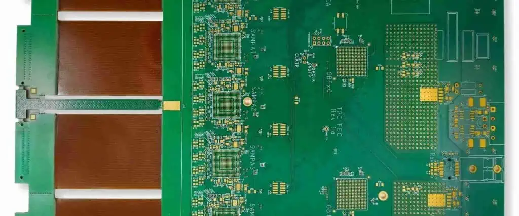
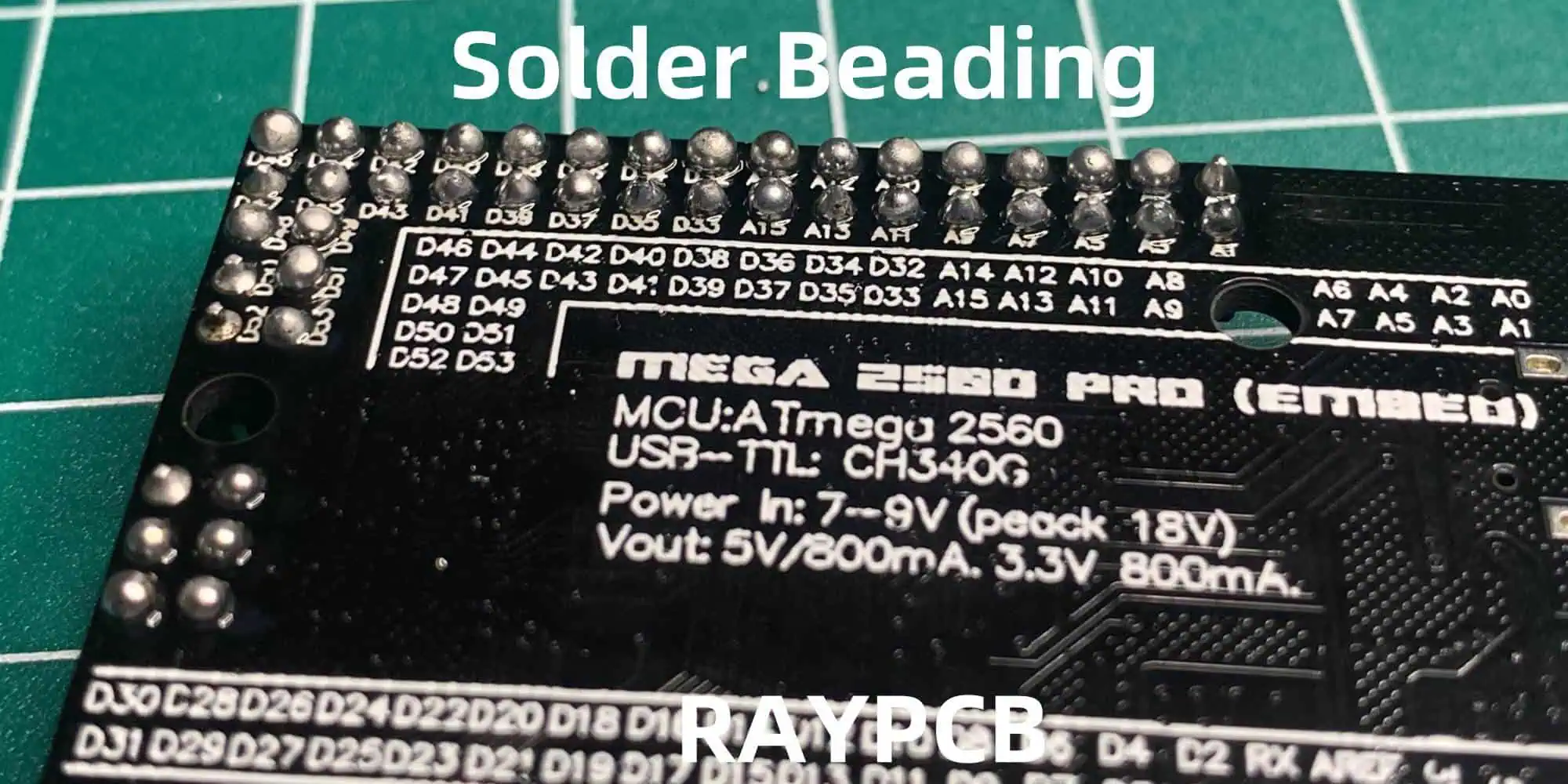
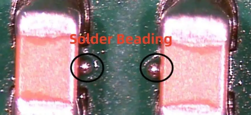
Solder beading, also known as solder balling or solder splatter, refers to the formation of small, spherical particles of solder that appear on a PCB during the soldering process. These tiny balls of solder, typically ranging from 0.1 to 0.3 mm in diameter, can be found scattered across the board surface, often in areas where they are not intended to be.

The Soldering Process

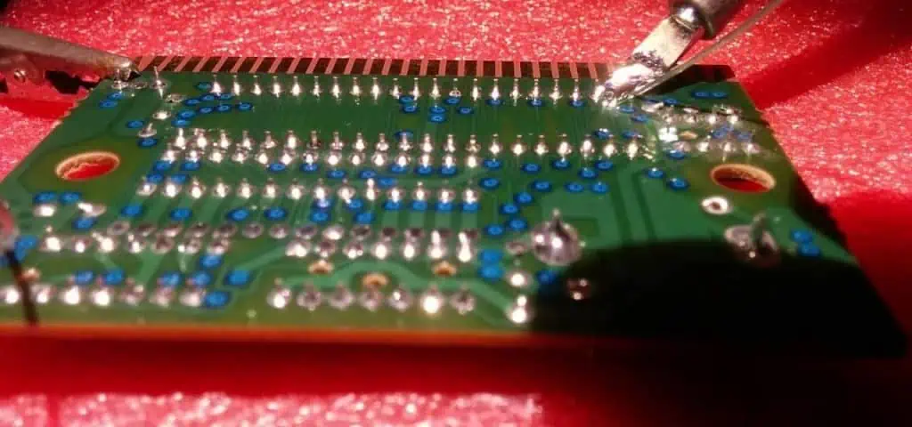
To understand solder beading, it’s essential to have a basic grasp of the soldering process. Soldering is a method of joining metal parts using a filler metal (solder) with a lower melting point than the base metals being joined. In PCB assembly, this process is used to create electrical connections between components and the board.

The typical steps in the soldering process include:

  1. Application of solder paste to the PCB pads
  2. Placement of components onto the board
  3. Heating the assembly to melt the solder (reflow soldering)
  4. Cooling to solidify the solder joints

It’s during the heating and cooling phases that solder beading can occur.

Types of Solder Beading

Solder beading can manifest in several forms:

  1. Mid-chip beading: Occurs under components, particularly between leads
  2. Peripheral beading: Forms around the edges of components
  3. Random beading: Appears scattered across the board surface
  4. Aligned beading: Forms in a linear pattern, often along board features

Causes of Solder Beading

Solder Paste-Related Factors

The characteristics and quality of the solder paste play a significant role in the occurrence of solder beading:

  1. Excessive solder paste: Overapplication can lead to excess solder forming beads
  2. Solder paste viscosity: Incorrect viscosity can affect the paste’s behavior during reflow
  3. Metal content: Higher metal content in the paste can increase the likelihood of beading
  4. Flux activity: Insufficient flux activity may fail to properly clean and wet surfaces

PCB Design Factors

The design of the PCB itself can contribute to solder beading:

  1. Pad design: Oversized or poorly designed pads can lead to excess solder
  2. Component spacing: Inadequate spacing can cause solder bridging and beading
  3. Solder mask definition: Poor solder mask design can affect solder paste deposition

Process-Related Factors

The soldering process and equipment used can influence solder beading:

  1. Reflow profile: Incorrect temperature profiles can cause solder to splatter
  2. Conveyor speed: Too rapid movement can disturb molten solder
  3. Nitrogen atmosphere: Lack of or excessive nitrogen can affect solder behavior
  4. Equipment maintenance: Poorly maintained equipment can lead to inconsistent results

Environmental Factors

Environmental conditions in the manufacturing facility can also play a role:

  1. Humidity: High humidity can affect solder paste properties
  2. Temperature fluctuations: Can impact the consistency of the soldering process
  3. Contamination: Airborne particles can interfere with solder joint formation

Effects of Solder Beading

Electrical Issues

Solder beading can lead to various electrical problems in the assembled PCB:

  1. Short circuits: Beads can create unintended connections between conductors
  2. Signal interference: Beads near high-frequency traces can cause signal distortion
  3. Increased capacitance: Beads can alter the capacitance between board features

Mechanical Issues

The presence of solder beads can also cause mechanical problems:

  1. Component misalignment: Beads can push components out of position
  2. Reduced clearance: Beads can interfere with the assembly of the final product
  3. Stress points: Beads can create areas of mechanical stress on the board

Reliability Concerns

Solder beading can have long-term implications for product reliability:

  1. Reduced insulation resistance: Beads can compromise the insulation between conductors
  2. Potential for migration: Over time, beads may move and cause new issues
  3. Increased susceptibility to environmental factors: Beads can trap contaminants

Cosmetic Issues

While not always functionally problematic, solder beading can affect the appearance of the product:

  1. Visual defects: Visible beads can be perceived as quality issues by customers
  2. Inconsistent appearance: Can lead to rejection in industries with strict visual standards

Prevention and Mitigation of Solder Beading

Solder Paste Optimization

Proper selection and handling of solder paste can significantly reduce the occurrence of beading:

  1. Use high-quality solder paste with appropriate metal content
  2. Ensure proper storage and handling to maintain paste characteristics
  3. Optimize paste application volume and method

PCB Design Considerations

Implementing design-for-manufacturing (DFM) principles can help prevent solder beading:

  1. Optimize pad sizes and shapes for each component
  2. Ensure adequate spacing between components and features
  3. Design solder masks to precisely control solder paste deposition

Process Optimization

Refining the soldering process is crucial in preventing solder beading:

  1. Develop and maintain optimal reflow profiles
  2. Implement proper nitrogen atmosphere control
  3. Regularly calibrate and maintain soldering equipment

Environmental Control

Maintaining a controlled manufacturing environment can reduce solder beading:

  1. Implement humidity control measures
  2. Maintain consistent ambient temperature
  3. Use air filtration systems to minimize contamination

Detection and Inspection Methods

Visual Inspection

Manual and automated visual inspection techniques can be used to detect solder beading:

  1. Manual microscopic inspection
  2. Automated optical inspection (AOI) systems
  3. High-magnification cameras for detailed examination

X-ray Inspection

X-ray inspection can reveal solder beading hidden under components:

  1. 2D X-ray systems for general inspection
  2. 3D X-ray tomography for detailed analysis of complex assemblies

Electrical Testing

Various electrical tests can help identify issues caused by solder beading:

  1. In-circuit testing (ICT) for detecting short circuits
  2. Functional testing to identify performance issues
  3. High-frequency testing for signal integrity problems

Industry Standards and Specifications

Several industry standards address solder beading and related defects:

  1. IPC-A-610: Acceptability of Electronic Assemblies
  2. J-STD-001: Requirements for Soldered Electrical and Electronic Assemblies
  3. IPC-7095: Design and Assembly Process Implementation for BGAs

These standards provide guidelines for acceptable levels of solder beading and methods for classification and mitigation.

Solder Beading in Different Soldering Technologies
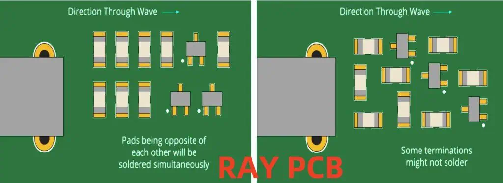
Wave Soldering

In wave soldering, solder beading can occur due to:

  1. Excessive wave height
  2. Improper pallet design
  3. Contamination in the solder pot

Reflow Soldering

Reflow soldering is particularly prone to solder beading due to:

  1. Solder paste characteristics
  2. Reflow profile issues
  3. Component outgassing

Selective Soldering

Selective soldering may experience solder beading due to:

  1. Improper nozzle design or maintenance
  2. Inconsistent solder flow
  3. Board warpage during the process

Impact of Miniaturization on Solder Beading

As electronic devices continue to shrink, the challenges associated with solder beading become more pronounced:

  1. Reduced spacing between components increases the risk of shorts
  2. Smaller solder joints are more susceptible to defects
  3. Inspection becomes more challenging as bead sizes decrease

Solder Beading in Advanced Packaging Technologies

BGA
BGA

Ball Grid Arrays (BGAs)

BGAs present unique challenges for solder beading:

  1. Hidden solder joints make inspection difficult
  2. Large number of connections increases the probability of defects
  3. Warpage during reflow can exacerbate beading issues

Chip Scale Packages (CSPs)

CSPs face similar issues to BGAs, but on a smaller scale:

  1. Extremely fine pitch increases the risk of bridging and beading
  2. Smaller solder volumes are more sensitive to process variations

Flip Chip Technology

Flip chip assemblies can experience solder beading due to:

  1. Underfill material interactions
  2. Thermal mismatch between chip and substrate
  3. Complex reflow profiles required for assembly

Economic Impact of Solder Beading

The occurrence of solder beading can have significant economic implications:

  1. Increased rework and repair costs
  2. Higher scrap rates in production
  3. Potential field failures and warranty claims
  4. Damage to company reputation due to quality issues

To illustrate the potential costs, consider the following table:

Impact AreaEstimated Cost (per 1000 boards)
Rework$500 – $2000
Scrap$1000 – $5000
Field Failures$5000 – $50000
Reputation DamageDifficult to quantify

These figures can vary widely depending on the product complexity, volume, and industry.

Future Trends in Solder Beading Management

As the electronics industry continues to evolve, several trends are emerging in the management of solder beading:

  1. Advanced simulation tools for predicting and preventing beading
  2. Development of new solder alloys and paste formulations
  3. Integration of AI and machine learning in inspection processes
  4. Implementation of Industry 4.0 principles for real-time process control

Conclusion

Solder beading, while a seemingly small defect, can have far-reaching consequences in the world of electronics manufacturing. Understanding its causes, effects, and prevention methods is crucial for producing high-quality, reliable electronic devices. As technology continues to advance, with components becoming smaller and more densely packed, the challenges associated with solder beading will likely increase.

However, with ongoing research, improved materials, and advanced manufacturing techniques, the industry is well-positioned to tackle these challenges. By implementing best practices in design, process control, and inspection, manufacturers can minimize the occurrence of solder beading and its impact on product quality and reliability.

As we move into an era of increasingly sophisticated electronic devices, the management of defects like solder beading will play a critical role in ensuring the continued advancement and reliability of technology that has become integral to our daily lives.

Frequently Asked Questions (FAQ)

  1. Q: How does solder beading differ from solder bridging? A: While both are soldering defects, they differ in nature and appearance. Solder beading refers to the formation of small, spherical particles of solder scattered on the PCB surface or under components. Solder bridging, on the other hand, occurs when excess solder forms a connection between two adjacent solder joints or pads that should remain electrically isolated. Bridging creates a direct short circuit, while beading may or may not cause immediate electrical issues depending on the location and size of the beads.
  2. Q: Can solder beading occur in lead-free soldering processes? A: Yes, solder beading can occur in both leaded and lead-free soldering processes. In fact, lead-free solders often have a higher melting point and different surface tension characteristics compared to traditional lead-based solders, which can sometimes make them more prone to beading. The transition to lead-free soldering has required adjustments in paste formulations, reflow profiles, and process controls to manage issues like solder beading.
  3. Q: How small can solder beads be, and at what size do they become a concern? A: Solder beads can vary in size, typically ranging from as small as 0.1 mm to 0.3 mm in diameter. However, with advancing miniaturization in electronics, even smaller beads can be problematic. Generally, any visible bead is a potential concern, as it represents a process deviation. The level of concern increases with bead size and proximity to other conductive elements on the board. In high-reliability applications or with very fine-pitch components, even beads as small as 0.05 mm could be significant.
  4. Q: Are there any situations where solder beading is considered acceptable? A: While solder beading is generally considered a defect, there are situations where very minor beading might be deemed acceptable, depending on the product’s requirements and applicable industry standards. For example, IPC-A-610, a widely used standard for electronics assemblies, defines different classes of products with varying acceptability criteria. In some cases, isolated, small beads that do not pose a risk of short circuits or other functional issues might be acceptable for less critical applications. However, for high-reliability products like medical devices or aerospace electronics, any solder beading is typically considered unacceptable.
  5. Q: How has the advent of 5G technology impacted concerns about solder beading? A: The introduction of 5G technology has heightened concerns about solder beading due to several factors:
    1. Higher frequencies: 5G operates at much higher frequencies than previous generations, making signal integrity more susceptible to small physical defects like solder beads.
    2. Increased component density: 5G devices often require more components in a smaller space, increasing the risk and potential impact of solder beading.
    3. Stricter performance requirements: 5G systems have more stringent performance criteria, making even small defects potentially significant.
    4. New materials and designs: The implementation of 5G has led to the use of new PCB materials and designs, which may require adjusted soldering processes to prevent beading.
    As a result, manufacturers working on 5G technology must be particularly vigilant in preventing and detecting solder beading to ensure optimal performance and reliability of these advanced systems.

What is the Coefficient of Thermal Expansion (CTE) in a PCB?

In the world of electronics manufacturing, understanding the physical properties of materials is crucial for designing reliable and long-lasting products. One of the most important properties to consider when dealing with Printed Circuit Boards (PCBs) is the Coefficient of Thermal Expansion (CTE). This property plays a significant role in determining the performance and reliability of PCBs, especially in applications where temperature fluctuations are common.

This article will delve into the concept of CTE, its importance in PCB design and manufacturing, and how it affects the overall performance of electronic devices. We’ll explore the various factors that influence CTE, methods for measuring and controlling it, and best practices for managing CTE in PCB design.

Understanding the Coefficient of Thermal Expansion

Definition of CTE

The Coefficient of Thermal Expansion (CTE) is a measure of how much a material expands or contracts with changes in temperature. It is typically expressed as the fractional change in size per degree of temperature change. In the context of PCBs, CTE is usually measured in parts per million per degree Celsius (ppm/ยฐC).

The Physics Behind CTE

At the atomic level, CTE is a result of the increased vibration of atoms as temperature rises. As atoms vibrate more vigorously, they require more space, causing the material to expand. Conversely, as temperature decreases, atomic vibrations decrease, leading to material contraction.

Types of CTE

There are three main types of CTE that are relevant to PCB design:

  1. Linear CTE: Measures expansion in one dimension
  2. Area CTE: Measures expansion in two dimensions
  3. Volumetric CTE: Measures expansion in three dimensions

For PCBs, the linear and area CTEs are most commonly used, as boards are primarily concerned with expansion in the x, y, and z directions.

The Importance of CTE in PCB Design

Thermal Stress and Reliability

One of the primary reasons CTE is crucial in PCB design is its impact on thermal stress. When different materials with varying CTEs are combined in a PCB, temperature changes can lead to mechanical stress at the interfaces between these materials. This stress can cause a variety of reliability issues, including:

  1. Solder joint fatigue
  2. Component cracking
  3. Delamination of PCB layers
  4. Warpage of the board

Impact on Electrical Performance

CTE can also affect the electrical performance of a PCB. As materials expand and contract, the following issues may arise:

  1. Changes in impedance of transmission lines
  2. Alterations in capacitance between conductors
  3. Variations in the dielectric constant of insulating materials

These changes can lead to signal integrity problems, especially in high-frequency applications.

Manufacturing Considerations

CTE plays a significant role in the PCB manufacturing process, particularly during:

  1. Lamination: Mismatched CTEs can cause warpage during the high-temperature lamination process.
  2. Soldering: Differences in CTE between components and the board can lead to solder joint reliability issues.
  3. Assembly: CTE mismatches can cause alignment problems during pick-and-place operations.

Factors Affecting CTE in PCBs

Material Composition

The CTE of a PCB is primarily determined by the materials used in its construction. Common PCB materials and their typical CTE values include:

MaterialCTE (ppm/ยฐC)
FR-4 (x-y direction)14-17
FR-4 (z direction)50-70
Polyimide12.-16
PTFE100-280
Copper17
Aluminum23
Silicon2.6

Layer Stack-up

The overall CTE of a multilayer PCB is influenced by the arrangement and thickness of its layers. Factors to consider include:

  1. The ratio of copper to dielectric material
  2. The orientation of fiberglass weave in FR-4 boards
  3. The use of constraining cores or stiffeners

Temperature Range

It’s important to note that CTE is not always constant across all temperature ranges. Some materials exhibit different expansion rates at different temperatures, which can complicate PCB design for applications with wide temperature ranges.

Moisture Content

The presence of moisture in PCB materials can affect their CTE. Absorbed moisture can cause materials to swell, altering their expansion characteristics.

Measuring and Controlling CTE in PCBs

Measurement Techniques

Several methods are used to measure CTE in PCB materials:

  1. Thermomechanical Analysis (TMA): Measures dimensional changes in a sample as it is heated or cooled.
  2. Dilatometry: Uses a high-precision instrument to measure length changes in a sample over a temperature range.
  3. Interferometry: Utilizes light interference patterns to detect minute changes in dimensions.

CTE Control Strategies

To manage CTE in PCB design, several strategies can be employed:

  1. Material Selection: Choosing materials with compatible CTEs for different layers and components.
  2. Symmetrical Design: Balancing the PCB stack-up to minimize warpage.
  3. Use of Constraining Cores: Incorporating low-CTE materials in the stack-up to reduce overall expansion.
  4. Thermal Management: Implementing effective heat dissipation to minimize temperature fluctuations.

CTE Matching in PCB Design

Board-to-Component Matching

One of the most critical aspects of CTE management in PCB design is matching the expansion rates of the board to those of the components. This is particularly important for:

  1. Ball Grid Array (BGA) packages
  2. Large integrated circuits
  3. Surface-mount components with a large footprint

Mismatches in CTE between the board and components can lead to solder joint fatigue and eventual failure.

Strategies for CTE Matching

To achieve better CTE matching, designers can:

  1. Use low-CTE laminates for critical areas of the board
  2. Implement selective use of high-Tg (glass transition temperature) materials
  3. Design with compliant lead structures for components
  4. Utilize underfill materials to distribute stress in BGA packages

CTE Considerations for Different PCB Applications

fr4 thermal conductivity

High-Reliability Applications

In applications where reliability is paramount, such as aerospace or medical devices, CTE management is critical. Strategies for these applications include:

  1. Use of polyimide or other low-CTE materials
  2. Extensive thermal cycling testing
  3. Implementation of redundant design features

High-Temperature Applications

For PCBs that operate in high-temperature environments, special considerations for CTE include:

  1. Selection of materials with stable CTEs at elevated temperatures
  2. Use of ceramic or metal-core PCBs for better thermal management
  3. Implementation of stress-relief design features

Flexible and Rigid-Flex PCBs

Flexible and rigid-flex PCBs present unique challenges for CTE management due to the combination of different materials. Considerations include:

  1. Matching CTEs between rigid and flexible sections
  2. Designing transition zones to manage stress
  3. Selecting adhesives that can accommodate CTE differences

Advanced Topics in CTE Management

Finite Element Analysis (FEA)

Finite Element Analysis is a powerful tool for predicting the effects of CTE in complex PCB designs. FEA can help designers:

  1. Identify areas of high stress due to CTE mismatches
  2. Optimize component placement and board layout
  3. Evaluate the effectiveness of different CTE management strategies

Novel Materials for CTE Control

Research into new materials for PCB manufacturing is ongoing, with a focus on improving CTE characteristics. Some promising developments include:

  1. Carbon fiber reinforced laminates
  2. Liquid crystal polymer (LCP) materials
  3. Ceramic-filled composites

These materials offer the potential for better CTE matching and improved thermal performance.

CTE in High-Frequency Applications

For high-frequency and microwave applications, CTE management becomes even more critical due to the sensitivity of these circuits to dimensional changes. Considerations include:

  1. Use of low-loss, low-CTE materials like PTFE composites
  2. Careful control of dielectric thickness variations
  3. Implementation of temperature compensation techniques in circuit design

Best Practices for CTE Management in PCB Design

Design Guidelines

To effectively manage CTE in PCB design, consider the following guidelines:

  1. Start with CTE considerations early in the design process
  2. Use symmetrical layer stack-ups whenever possible
  3. Pay special attention to CTE matching for large components
  4. Implement thermal relief patterns for better stress distribution
  5. Use via-in-pad designs cautiously, as they can exacerbate CTE-related stress

Material Selection Criteria

When selecting materials for a PCB design, consider the following CTE-related factors:

  1. CTE values in x, y, and z directions
  2. CTE stability across the expected temperature range
  3. Glass transition temperature (Tg) of the material
  4. Moisture absorption characteristics
  5. Compatibility with other materials in the design

Testing and Validation

To ensure that CTE-related issues are properly addressed, consider implementing the following testing and validation procedures:

  1. Thermal cycling tests to simulate real-world conditions
  2. X-ray inspection of solder joints after thermal stress
  3. Warpage measurements at different temperatures
  4. Electrical testing across the operating temperature range

Future Trends in CTE Management

Emerging Technologies

As the electronics industry continues to evolve, new technologies are emerging that may impact CTE management in PCBs:

  1. 3D-printed electronics with custom CTE profiles
  2. Embedded components for reduced surface CTE stress
  3. Advanced thermal management materials and techniques

Sustainability Considerations

As the industry moves towards more sustainable practices, CTE management may be influenced by:

  1. The development of bio-based PCB materials with unique CTE properties
  2. Increased focus on recyclable and repairable designs
  3. Implementation of life cycle assessment tools that consider CTE-related reliability factors

Conclusion

Understanding and managing the Coefficient of Thermal Expansion is crucial for designing reliable and high-performance PCBs. As electronic devices continue to become more compact and operate in more demanding environments, the importance of CTE management will only increase.

By considering CTE throughout the design process, selecting appropriate materials, and implementing effective testing and validation procedures, PCB designers can create boards that maintain their integrity and performance across a wide range of temperatures and operating conditions.

As new materials and technologies emerge, the field of CTE management in PCBs will continue to evolve, offering new opportunities for innovation and improved reliability in electronic devices.

Frequently Asked Questions (FAQ)

  1. Q: How does CTE affect the reliability of solder joints in a PCB? A: CTE differences between the PCB and components can cause stress on solder joints during temperature changes. This stress can lead to fatigue and eventual failure of the joints, especially in applications with frequent thermal cycling. To mitigate this, designers must carefully consider CTE matching between the board and components, and may implement strategies such as using compliant lead structures or underfill materials.
  2. Q: What is the significance of the glass transition temperature (Tg) in relation to CTE? A: The glass transition temperature (Tg) is the point at which a polymer transitions from a rigid to a more flexible state. This transition is often accompanied by a significant change in CTE. Below Tg, materials typically have a lower and more stable CTE, while above Tg, the CTE can increase dramatically. Understanding the Tg of PCB materials is crucial for predicting their behavior across different temperature ranges and ensuring reliable performance.
  3. Q: How do you manage CTE in a multilayer PCB with different materials? A: Managing CTE in multilayer PCBs with different materials involves several strategies:
    • Using a symmetrical layer stack-up to balance stress
    • Selecting materials with compatible CTEs
    • Incorporating low-CTE constraining cores
    • Carefully considering the thickness and placement of different materials
    • Using modeling and simulation tools to predict and optimize CTE behavior The goal is to create a balanced design that minimizes overall warpage and stress concentrations.
  4. Q: What are the challenges of CTE management in high-frequency PCB applications? A: High-frequency PCB applications face unique CTE challenges due to their sensitivity to dimensional changes. Key issues include:
    • Maintaining consistent impedance in transmission lines as dimensions change
    • Preserving the stability of the dielectric constant across temperature ranges
    • Minimizing signal skew caused by differential expansion
    • Ensuring reliable connections for sensitive high-frequency components To address these challenges, designers often use specialized low-CTE, low-loss materials and implement careful thermal management strategies.
  5. Q: How does moisture absorption in PCB materials affect CTE? A: Moisture absorption can significantly impact the CTE of PCB materials, particularly in polymer-based substrates like FR-4. As materials absorb moisture, they can swell, altering their dimensions and effective CTE. This can lead to several issues:
    • Increased warpage and stress in the board
    • Changes in electrical properties, such as dielectric constant
    • Potential delamination during high-temperature processes like soldering To mitigate these effects, designers must consider moisture absorption characteristics when selecting materials and may implement measures such as baking boards before assembly or using moisture-resistant coatings.

Rogers Releases New Waterproof Flexible Heater Substrate for Flex Heater Applications

Introduction

In a significant development for the flexible heater industry, Rogers Corporation has unveiled its latest innovation: a new waterproof flexible heater substrate designed specifically for flex heater applications. This breakthrough product promises to revolutionize the way manufacturers approach flexible heating solutions, offering enhanced performance, durability, and versatility across a wide range of industries and applications.

Understanding Flexible Heaters and Their Applications

What are Flexible Heaters?

Flexible heaters are thin, lightweight heating elements that can conform to various shapes and surfaces. They are designed to provide efficient and uniform heat distribution in applications where traditional rigid heating elements are impractical or inefficient.

Key Applications of Flexible Heaters

Flexible heaters find use in numerous industries and applications, including:

  1. Aerospace and aviation
  2. Automotive
  3. Medical devices
  4. Food service equipment
  5. Industrial processes
  6. Consumer electronics
  7. Outdoor gear and clothing

Advantages of Flexible Heaters

The popularity of flexible heaters stems from several key advantages:

  • Conformability to complex shapes
  • Uniform heat distribution
  • Lightweight and space-saving design
  • Rapid heating and cooling
  • Energy efficiency
  • Customizable to specific requirements

Rogers Corporation: A Leader in Advanced Materials

Company Background

Rogers Corporation has been at the forefront of engineered materials solutions for over 180 years. The company specializes in developing and manufacturing high-performance materials for various industries, including electronics, automotive, and aerospace.

Expertise in Flexible Materials

Rogers has a long history of innovation in flexible materials, including:

  • Flexible circuit materials
  • Elastomeric materials
  • High-frequency laminates
  • Thermal management solutions

This extensive experience and expertise have positioned Rogers as a trusted provider of advanced materials for flexible heater applications.

The New Waterproof Flexible Heater Substrate

Product Overview

Rogers’ new waterproof flexible heater substrate represents a significant advancement in flexible heater technology. This innovative material is designed to meet the growing demand for reliable, high-performance heating solutions in challenging environments.

Key Features and Benefits

Waterproof Design

  • Resistant to water ingress and moisture damage
  • Suitable for use in wet or humid environments
  • Improved reliability and longevity

Flexibility and Conformability

  • Ability to bend and flex without compromising performance
  • Conforms to complex shapes and contours
  • Enables design freedom for engineers and product developers

Enhanced Thermal Performance

  • Efficient heat transfer and distribution
  • Rapid heating and cooling capabilities
  • Uniform temperature across the heating surface

Durability and Reliability

  • Resistant to mechanical stress and fatigue
  • Stable performance over a wide temperature range
  • Long operational life

Customizability

  • Available in various thicknesses and dimensions
  • Compatible with different heating element designs
  • Adaptable to specific application requirements

Technical Specifications

PropertyValue
Operating Temperature Range-40ยฐC to 150ยฐC
Dielectric Strength>1000 V/mil
Thermal Conductivity0.5 W/mยทK
Water Absorption<0.1%
Flexibility (Minimum Bend Radius)3mm
Available Thicknesses0.1mm to 2.0mm

Note: Specific values may vary depending on the exact product variant and configuration.

Applications of the New Waterproof Flexible Heater Substrate

Flexible PCB Assembly

Automotive Industry

Battery Thermal Management

  • Efficient heating of electric vehicle batteries in cold conditions
  • Improved battery performance and range

Sensor and Camera Defrosting

  • Reliable operation of autonomous driving systems in adverse weather
  • Enhanced safety and functionality of vehicle sensors

Seat Heating

  • Comfortable and energy-efficient seat warming systems
  • Improved passenger comfort in cold climates

Aerospace and Aviation

De-icing Systems

  • Efficient and lightweight de-icing solutions for aircraft wings and surfaces
  • Enhanced safety and reliability in cold weather operations

Cabin Comfort

  • Flexible heating elements for passenger seating and cabin walls
  • Improved passenger comfort and energy efficiency

Medical Devices

Patient Warming Systems

  • Gentle and uniform heating for surgical tables and recovery beds
  • Enhanced patient comfort and temperature management

Portable Medical Equipment

  • Reliable heating for portable diagnostic and treatment devices
  • Improved performance in various environmental conditions

Outdoor and Recreational Equipment

Heated Clothing and Gear

  • Flexible and durable heating elements for jackets, gloves, and boots
  • Enhanced comfort and safety in extreme cold conditions

Camping and Expedition Equipment

  • Reliable heating solutions for tents, sleeping bags, and portable shelters
  • Improved functionality and comfort in outdoor environments

Industrial Applications

Process Heating

  • Flexible heating solutions for tanks, pipes, and vessels
  • Improved efficiency and temperature control in industrial processes

Moisture and Condensation Prevention

  • Reliable heating to prevent moisture accumulation in sensitive equipment
  • Enhanced durability and performance of industrial machinery

Manufacturing Process and Quality Control

Material Composition

The new waterproof flexible heater substrate is composed of a proprietary blend of polymers and additives, carefully engineered to achieve the desired balance of flexibility, thermal performance, and water resistance.

Manufacturing Techniques

Rogers employs advanced manufacturing techniques to produce the substrate, including:

  1. Precision extrusion
  2. Controlled lamination processes
  3. Surface treatment for enhanced adhesion
  4. Rigorous quality control inspections

Quality Assurance Measures

To ensure consistent high quality, Rogers implements a comprehensive quality assurance program, including:

  • In-line process monitoring
  • Regular material testing and characterization
  • Batch sampling and analysis
  • Accelerated aging and environmental stress testing

Comparison with Existing Technologies

Traditional Flexible Heater Substrates

PropertyNew Waterproof SubstrateTraditional Substrates
Water ResistanceExcellentLimited to Poor
FlexibilityHighModerate to High
Temperature Range-40ยฐC to 150ยฐCTypically -30ยฐC to 120ยฐC
DurabilityExcellentGood
CustomizabilityHighModerate

Advantages Over Competing Solutions

  • Superior water resistance and reliability in wet environments
  • Extended operating temperature range
  • Improved flexibility and conformability
  • Enhanced durability and longevity
  • Greater design freedom and customization options

Environmental and Sustainability Considerations

Energy Efficiency

The new substrate’s efficient heat transfer properties contribute to reduced energy consumption in heating applications, aligning with global efforts to improve energy efficiency and reduce carbon emissions.

Material Sustainability

Rogers is committed to sustainable manufacturing practices and has implemented measures to minimize the environmental impact of production, including:

  • Use of recyclable and eco-friendly materials where possible
  • Reduction of waste and energy consumption in manufacturing processes
  • Compliance with global environmental regulations and standards

Product Lifecycle Considerations

The durability and long operational life of the new substrate contribute to reduced waste and resource consumption over time, as fewer replacements are needed compared to less durable alternatives.

Future Developments and Research Directions

Ongoing Research and Development

Rogers continues to invest in research and development to further enhance the performance and capabilities of its flexible heater substrates. Areas of focus include:

  • Improved thermal conductivity
  • Enhanced flexibility and stretchability
  • Integration of smart features and sensors
  • Exploration of bio-based and biodegradable materials

Potential Future Applications

As technology advances, new applications for waterproof flexible heater substrates are likely to emerge, including:

  • Advanced wearable technologies
  • Next-generation electric vehicles
  • Flexible electronics and displays
  • Biomedical implants and devices
  • Smart textiles and garments

Industry Impact and Market Outlook

Market Potential

The global flexible heater market is expected to experience significant growth in the coming years, driven by factors such as:

  • Increasing demand for electric vehicles
  • Growth in wearable technology and smart devices
  • Advancements in medical devices and healthcare technology
  • Expansion of industrial automation and IoT applications

Competitive Landscape

Rogers’ new waterproof flexible heater substrate positions the company as a leader in this growing market. However, competition from other materials manufacturers and emerging technologies is expected to drive further innovation and market expansion.

Adoption Challenges and Opportunities

While the new substrate offers significant advantages, potential challenges to widespread adoption include:

  • Initial cost considerations
  • Need for education and awareness among engineers and designers
  • Regulatory approvals for specific applications

Opportunities for accelerated adoption include:

  • Partnerships with OEMs and product manufacturers
  • Demonstration projects showcasing the substrate’s capabilities
  • Customization and co-development initiatives with key customers

Conclusion

Rogers Corporation’s new waterproof flexible heater substrate represents a significant advancement in flexible heating technology. By combining superior water resistance with excellent thermal performance and flexibility, this innovative material opens up new possibilities for designers and engineers across a wide range of industries.

As the demand for reliable, efficient, and versatile heating solutions continues to grow, Rogers’ new substrate is well-positioned to play a crucial role in shaping the future of flexible heater applications. From automotive and aerospace to medical devices and outdoor equipment, the potential applications for this technology are vast and diverse.

With ongoing research and development efforts, we can expect to see further innovations and improvements in flexible heater substrates, driving the industry forward and enabling new technologies and products that were previously impossible or impractical.

As manufacturers and designers explore the possibilities offered by this new waterproof flexible heater substrate, we are likely to witness a new wave of innovation in heating solutions, contributing to improved performance, energy efficiency, and reliability across various applications and industries.

Frequently Asked Questions (FAQ)

Q1: What makes Rogers’ new flexible heater substrate waterproof?

A1: The new substrate is made from a proprietary blend of polymers and additives specifically engineered to resist water ingress and moisture damage. The material’s composition and manufacturing process create a highly water-resistant structure that maintains its properties even when exposed to wet or humid environments.

Q2: How does the flexibility of this new substrate compare to traditional options?

A2: Rogers’ new substrate offers superior flexibility compared to many traditional options, with a minimum bend radius of 3mm. This high degree of flexibility allows the substrate to conform to complex shapes and contours more easily, enabling greater design freedom and application versatility.

Q3: What temperature range can this new substrate withstand?

A3: The new waterproof flexible heater substrate has an operating temperature range of -40ยฐC to 150ยฐC. This wide range makes it suitable for a diverse array of applications, from extreme cold environments to high-temperature industrial processes.

Q4: Is the new substrate compatible with different types of heating elements?

A4: Yes, the substrate is designed to be compatible with various heating element designs, including etched foil, wire wound, and printed elements. This versatility allows manufacturers to choose the most appropriate heating element technology for their specific application requirements.

Q5: How does this new substrate contribute to energy efficiency in heating applications?

A5: The substrate’s efficient heat transfer properties and uniform heat distribution capabilities contribute to improved energy efficiency in several ways. It allows for more precise temperature control, reduces heat loss, and enables faster heating and cooling cycles. These factors combine to minimize energy consumption while maintaining optimal heating performance.

RF Pool โ€“ Insights and Details: All You Need to Know

Radio Frequency (RF) technology is a fundamental component of modern wireless communication systems. From cellular networks to Wi-Fi and Bluetooth, RF plays a crucial role in our interconnected world. One concept that has gained significant attention in recent years is the RF pool. This article will delve deep into the world of RF pools, exploring their significance, applications, and impact on wireless communication technologies.

What is an RF Pool?

An RF pool, short for Radio Frequency Pool, refers to a collection of shared RF resources that can be dynamically allocated and managed to optimize wireless network performance. These resources typically include:

  1. Frequency bands
  2. Transmit power
  3. Antennas
  4. Signal processing capabilities

The primary goal of an RF pool is to improve spectrum efficiency, increase network capacity, and enhance overall system performance by intelligently distributing and utilizing available RF resources.

The Evolution of RF Resource Management

Traditional Approaches

Historically, RF resource management has been relatively static and inflexible. Traditional approaches include:

Fixed Frequency Allocation

  • Assigning specific frequency bands to particular services or operators
  • Limited ability to adapt to changing demand or interference conditions

Cell-Based Planning

  • Dividing geographical areas into cells with dedicated RF resources
  • Difficulty in handling uneven traffic distribution and hotspots

Manual Optimization

  • Periodic manual adjustments to network parameters
  • Time-consuming and often reactive rather than proactive

The Shift Towards Dynamic RF Pooling

As wireless networks have become more complex and demand has increased, there has been a shift towards more dynamic and flexible approaches to RF resource management:

Software-Defined Radio (SDR)

  • Enabling hardware to operate across a wide range of frequencies
  • Facilitating more flexible resource allocation

Cognitive Radio

  • Allowing devices to sense and adapt to their RF environment
  • Improving spectrum utilization and reducing interference

Cloud-Based Radio Access Networks (C-RAN)

  • Centralizing baseband processing and resource management
  • Enabling more coordinated and efficient use of RF resources

Key Components of an RF Pool

An effective RF pool system comprises several key components working together to optimize resource allocation:

Resource Inventory

  • Comprehensive database of available RF resources
  • Real-time tracking of resource status and utilization

Allocation Algorithms

  • Sophisticated algorithms for dynamic resource assignment
  • Consideration of factors such as traffic demand, interference, and quality of service requirements

Monitoring and Analytics

  • Continuous monitoring of network performance and resource utilization
  • Advanced analytics for identifying trends and optimization opportunities

Control and Management Interface

  • Centralized platform for managing and configuring the RF pool
  • Integration with existing network management systems

Virtualization Layer

  • Abstraction of physical RF resources into virtual resources
  • Enabling flexible allocation and sharing across multiple services or operators

Benefits of RF Pooling

Implementing an RF pool approach offers numerous advantages for wireless network operators and users:

Improved Spectrum Efficiency

  • Maximizing the use of available frequency bands
  • Reducing spectrum waste and underutilization

Enhanced Network Capacity

  • Dynamic allocation of resources to meet varying demand
  • Ability to handle traffic spikes and hotspots more effectively

Better Quality of Service

  • Optimizing resource allocation based on service requirements
  • Reducing interference and improving signal quality

Cost Reduction

  • More efficient use of existing infrastructure
  • Potential reduction in equipment and operational costs

Increased Flexibility and Scalability

  • Easier adaptation to new technologies and services
  • Simplified network expansion and upgrades

Energy Efficiency

  • Optimizing power allocation based on actual demand
  • Potential for reducing overall energy consumption

Applications of RF Pooling

RF Hardware Engineer

RF pooling concepts are being applied across various wireless communication domains:

5G and Beyond

  • Enabling dynamic spectrum sharing between different services
  • Supporting diverse use cases with varying resource requirements

Internet of Things (IoT)

  • Efficiently managing large numbers of low-power devices
  • Optimizing resource allocation for sporadic and bursty IoT traffic

Private Networks

  • Facilitating the deployment of enterprise and industrial wireless networks
  • Enabling efficient resource sharing between different applications

Satellite Communications

  • Optimizing the use of limited satellite spectrum resources
  • Supporting flexible allocation for varying geographical demand

Public Safety Networks

  • Ensuring critical communication resources are available when needed
  • Enabling dynamic prioritization during emergencies

Challenges in Implementing RF Pools

While RF pooling offers significant benefits, there are several challenges that need to be addressed:

Technical Complexity

  • Developing sophisticated algorithms for real-time resource allocation
  • Ensuring seamless integration with existing network infrastructure

Regulatory Constraints

  • Navigating spectrum licensing and regulatory requirements
  • Addressing potential concerns about interference and fairness

Interoperability

  • Ensuring compatibility between different vendors and technologies
  • Developing and adhering to industry standards for RF pooling

Security and Privacy

  • Protecting shared resources from unauthorized access or manipulation
  • Ensuring data privacy in multi-tenant environments

Performance Overhead

  • Managing the computational and signaling overhead of dynamic allocation
  • Minimizing latency in resource assignment decisions

RF Pool Architecture

A typical RF pool architecture consists of several layers working together to manage and allocate resources efficiently:

LayerFunctionComponents
Physical LayerRF hardware and infrastructureAntennas, amplifiers, filters
Virtualization LayerAbstraction of physical resourcesVirtual resource managers, hypervisors
Control LayerResource allocation and managementAllocation algorithms, monitoring systems
Service LayerUser and application interfaceAPI gateways, service orchestrators

This layered approach allows for flexible and scalable implementation of RF pooling concepts across different network types and technologies.

Implementation Strategies for RF Pooling

Successful implementation of RF pooling requires a strategic approach:

Assessment and Planning

  • Evaluate current network infrastructure and resource utilization
  • Identify key performance indicators and optimization goals

Pilot Implementation

  • Start with a small-scale deployment to validate concepts
  • Gather data on performance improvements and challenges

Gradual Rollout

  • Expand RF pooling implementation in phases
  • Continuously monitor and adjust based on real-world performance

Integration with Existing Systems

  • Ensure seamless integration with current network management tools
  • Develop interfaces for legacy systems where necessary

Training and Skill Development

  • Invest in training for network operators and engineers
  • Develop new skill sets for managing dynamic RF environments

Continuous Optimization

  • Implement processes for ongoing performance monitoring and optimization
  • Stay updated on emerging technologies and best practices

Future Trends in RF Pooling

As technology continues to evolve, several trends are shaping the future of RF pooling:

Artificial Intelligence and Machine Learning

  • AI-driven resource allocation and optimization
  • Predictive analytics for proactive network management

Edge Computing Integration

  • Distributed intelligence for faster and more localized decision-making
  • Enhanced coordination between edge and centralized resources

Open RAN and Virtualization

  • Increased disaggregation of network components
  • Greater flexibility in resource pooling across multi-vendor environments

Millimeter Wave and Terahertz Bands

  • Expansion of RF pooling concepts to higher frequency bands
  • New challenges and opportunities in resource management

Quantum Communication

  • Potential application of RF pooling concepts to quantum networks
  • Novel approaches to managing quantum entanglement as a resource

Case Studies: RF Pooling in Action

Mobile Network Operator in Urban Environment

A major mobile network operator implemented RF pooling in a densely populated urban area, resulting in:

  • 30% increase in network capacity
  • 25% reduction in dropped calls
  • 15% improvement in average data speeds

Industrial IoT Deployment

A large manufacturing facility adopted RF pooling for its industrial IoT network:

  • 40% reduction in spectrum usage
  • 50% decrease in network latency
  • Improved reliability for critical control systems

Public Safety Network

A regional public safety network implemented RF pooling to enhance emergency response capabilities:

  • 60% increase in available bandwidth during crisis situations
  • Seamless prioritization of critical communications
  • Improved interoperability between different agencies

Conclusion

RF pooling represents a significant advancement in wireless network resource management. By enabling dynamic and efficient allocation of RF resources, it offers the potential to dramatically improve network performance, capacity, and flexibility. As wireless technologies continue to evolve and demand for spectrum grows, RF pooling will play an increasingly crucial role in maximizing the utility of our limited RF resources.

While challenges remain in terms of implementation complexity and regulatory considerations, the benefits of RF pooling are clear. As the technology matures and best practices emerge, we can expect to see widespread adoption across various wireless communication domains. The future of wireless networks will undoubtedly be shaped by the intelligent and adaptive resource management enabled by RF pooling.

Frequently Asked Questions (FAQ)

Q1: What is the main difference between traditional RF management and RF pooling?

A1: Traditional RF management typically involves static allocation of resources, while RF pooling enables dynamic and flexible allocation based on real-time demand and network conditions. This allows for more efficient use of spectrum and improved network performance.

Q2: How does RF pooling contribute to improved spectrum efficiency?

A2: RF pooling improves spectrum efficiency by dynamically allocating resources where they are needed most, reducing waste and underutilization. It allows multiple services or users to share the same spectrum resources, maximizing their utility.

Q3: What are the main challenges in implementing RF pooling?

A3: Key challenges include technical complexity in developing allocation algorithms, regulatory constraints, ensuring interoperability between different systems, addressing security and privacy concerns, and managing the performance overhead of dynamic allocation.

Q4: How does AI and machine learning factor into RF pooling?

A4: AI and machine learning are increasingly being used to optimize resource allocation in RF pools. These technologies can predict network demand, identify patterns, and make intelligent decisions about resource distribution, leading to more efficient and adaptive network performance.

Q5: Can RF pooling be implemented in existing networks, or does it require new infrastructure?

A5: While RF pooling can be most effectively implemented in new network deployments, it is possible to introduce RF pooling concepts to existing networks through software upgrades and the addition of centralized management systems. The extent of implementation may depend on the existing infrastructure’s flexibility and capabilities.

Understanding the Importance of Front-End Data Optimization In PCB Assembly

In the rapidly evolving world of electronics manufacturing, printed circuit board (PCB) assembly plays a crucial role in creating the devices we use every day. As technology advances and products become more complex, the importance of efficient and accurate PCB assembly processes grows exponentially. One of the key factors in achieving high-quality, cost-effective PCB production is front-end data optimization. This article will explore the significance of front-end data optimization in PCB assembly, its impact on various aspects of the manufacturing process, and strategies for implementing effective optimization techniques.

What is Front-End Data Optimization?

Front-end data optimization in PCB assembly refers to the process of refining and enhancing the design and manufacturing data before it enters the production phase. This optimization involves several key steps:

  1. Design file preparation
  2. Component data management
  3. Manufacturing process planning
  4. Design for manufacturability (DFM) analysis
  5. Test and inspection strategy development

By focusing on these areas early in the PCB assembly process, manufacturers can significantly improve efficiency, reduce errors, and ultimately produce higher-quality products at lower costs.

The Impact of Front-End Data Optimization on PCB Assembly

High Volume Assembly Line

Improved Manufacturing Efficiency

One of the primary benefits of front-end data optimization is the substantial improvement in manufacturing efficiency. By addressing potential issues and optimizing design data before production begins, manufacturers can:

  • Reduce setup times
  • Minimize machine downtime
  • Streamline component placement
  • Optimize solder paste application
  • Enhance overall production throughput

These improvements translate directly into faster production cycles and increased capacity, allowing manufacturers to meet demanding schedules and take on more projects.

Enhanced Quality Control

Front-end data optimization plays a crucial role in ensuring the quality of the final PCB assembly. By identifying and addressing potential issues early in the process, manufacturers can:

  • Reduce defect rates
  • Improve first-pass yields
  • Enhance product reliability
  • Minimize rework and scrap

This proactive approach to quality control not only results in better products but also contributes to cost savings and improved customer satisfaction.

Cost Reduction

Optimizing front-end data can lead to significant cost reductions throughout the PCB assembly process. These savings come from various sources:

  • Reduced material waste
  • Lower rework and repair costs
  • Improved component utilization
  • Decreased machine setup and changeover times
  • Optimized production planning

By addressing these areas through front-end optimization, manufacturers can achieve substantial cost savings without compromising on quality or performance.

Faster Time-to-Market

In today’s competitive electronics market, reducing time-to-market is crucial for success. Front-end data optimization contributes to faster product launches by:

  • Minimizing design iterations
  • Reducing production delays
  • Streamlining the prototype-to-production transition
  • Enabling parallel processing of design and manufacturing tasks

These time savings can provide a significant competitive advantage, allowing companies to introduce new products more quickly and respond to market demands more effectively.

Key Components of Front-End Data Optimization

Design File Preparation

Proper preparation of design files is the foundation of effective front-end data optimization. This process involves:

CAD Data Cleaning and Normalization

  • Removing redundant or conflicting design elements
  • Standardizing layer naming conventions
  • Verifying design rule compliance

Design for Manufacturing (DFM) Analysis

  • Checking for manufacturability issues
  • Optimizing component placement and routing
  • Ensuring proper clearances and tolerances

Panelization Optimization

  • Determining the most efficient panel layout
  • Optimizing for material utilization and production efficiency
  • Considering test and breakout requirements

Component Data Management

Effective component data management is crucial for smooth PCB assembly. Key aspects include:

Bill of Materials (BOM) Optimization

  • Verifying component availability and lead times
  • Identifying alternative components for supply chain flexibility
  • Standardizing component descriptions and part numbers

Component Library Management

  • Maintaining up-to-date component footprints and models
  • Ensuring consistency across design and manufacturing data
  • Implementing version control for component libraries

Approved Vendor List (AVL) Management

  • Maintaining a curated list of approved suppliers
  • Ensuring component quality and reliability
  • Optimizing for cost and availability

Manufacturing Process Planning

Optimizing the manufacturing process plan is essential for efficient PCB assembly. This includes:

SMT Process Optimization

  • Determining optimal component placement sequences
  • Optimizing solder paste stencil design
  • Planning for efficient machine setup and changeover

Through-Hole Process Planning

  • Optimizing manual and automated insertion processes
  • Planning for wave soldering or selective soldering operations
  • Considering mixed-technology assembly requirements

Test and Inspection Strategy

  • Developing in-circuit test (ICT) and functional test plans
  • Optimizing automated optical inspection (AOI) programs
  • Planning for X-ray inspection of critical components

Strategies for Implementing Front-End Data Optimization

Leverage Advanced Software Tools

Utilizing specialized software tools can greatly enhance front-end data optimization efforts:

  • CAD/CAM integration software
  • DFM analysis tools
  • BOM management systems
  • Component library management software
  • Process planning and optimization tools

These tools can automate many aspects of the optimization process, improving accuracy and efficiency.

Establish Standardized Processes

Developing and implementing standardized processes for front-end data optimization ensures consistency and repeatability:

  • Create detailed checklists for design file preparation
  • Establish clear guidelines for component data management
  • Develop standard operating procedures for process planning
  • Implement quality control checkpoints throughout the optimization process

Foster Collaboration Between Design and Manufacturing Teams

Encouraging close collaboration between design and manufacturing teams can lead to significant improvements in front-end data optimization:

  • Conduct regular design reviews with manufacturing input
  • Implement feedback loops for continuous improvement
  • Provide cross-training opportunities to enhance understanding of both design and manufacturing considerations

Invest in Training and Skill Development

Ensuring that team members have the necessary skills and knowledge is crucial for effective front-end data optimization:

  • Provide training on advanced software tools
  • Offer workshops on DFM principles and best practices
  • Encourage participation in industry conferences and seminars
  • Develop internal knowledge-sharing initiatives

Implement Continuous Improvement Practices

Adopting a culture of continuous improvement can drive ongoing enhancements in front-end data optimization:

  • Regularly analyze production data to identify optimization opportunities
  • Encourage team members to suggest process improvements
  • Implement formal continuous improvement methodologies (e.g., Six Sigma, Lean)
  • Conduct periodic audits of optimization processes and outcomes

Measuring the Success of Front-End Data Optimization

To evaluate the effectiveness of front-end data optimization efforts, manufacturers should track key performance indicators (KPIs) such as:

KPI Description Target
First-Pass Yield Percentage of boards that pass initial testing without rework >95%
Defect Rate Number of defects per million opportunities (DPMO) <100 DPMO
Setup Time Time required to set up production for a new board design <2 hours
Time-to-Market Time from design completion to production readiness <4 weeks
Material Utilization Percentage of raw materials effectively used in production >95%

By monitoring these KPIs and comparing them to industry benchmarks, manufacturers can assess the impact of their front-end data optimization efforts and identify areas for further improvement.

Challenges in Front-End Data Optimization

While the benefits of front-end data optimization are clear, there are several challenges that manufacturers may face:

Data Integration and Compatibility

  • Ensuring seamless data transfer between different software systems
  • Managing multiple file formats and versions
  • Maintaining data integrity throughout the optimization process

Keeping Pace with Technological Advancements

  • Adapting to new component technologies and packaging types
  • Integrating emerging manufacturing processes and equipment
  • Updating optimization strategies for evolving design complexities

Balancing Optimization with Time Constraints

  • Meeting tight production schedules while ensuring thorough optimization
  • Allocating sufficient time and resources for front-end activities
  • Demonstrating the long-term value of optimization to stakeholders

Managing Complex Supply Chains

  • Optimizing for component availability and lead times
  • Adapting to supply chain disruptions and market fluctuations
  • Balancing cost considerations with quality and reliability requirements

Future Trends in Front-End Data Optimization

As technology continues to evolve, several trends are shaping the future of front-end data optimization in PCB assembly:

Artificial Intelligence and Machine Learning

  • AI-driven design rule checking and optimization
  • Machine learning algorithms for predictive process optimization
  • Automated component selection and substitution

Digital Twin Technology

  • Creating virtual representations of the entire PCB assembly process
  • Enabling real-time simulation and optimization of manufacturing processes
  • Facilitating predictive maintenance and quality control

Advanced Data Analytics

  • Leveraging big data analytics for continuous process improvement
  • Implementing real-time monitoring and adjustment of optimization parameters
  • Developing predictive models for yield and quality optimization

Cloud-Based Collaboration Tools

  • Enabling seamless collaboration between global design and manufacturing teams
  • Providing real-time access to optimization data and analytics
  • Facilitating version control and change management across the supply chain

Conclusion

Front-end data optimization is a critical factor in achieving efficient, high-quality PCB assembly. By focusing on optimizing design files, component data, and manufacturing processes before production begins, manufacturers can significantly improve efficiency, reduce costs, and enhance product quality. While challenges exist, the benefits of effective front-end data optimization far outweigh the initial investment required. As technology continues to advance, embracing new tools and methodologies for optimization will be crucial for staying competitive in the rapidly evolving electronics manufacturing industry.

Frequently Asked Questions (FAQ)

Q1: What are the key benefits of front-end data optimization in PCB assembly?

A1: The main benefits include improved manufacturing efficiency, enhanced quality control, cost reduction, and faster time-to-market. These advantages stem from addressing potential issues early in the process, optimizing design and component data, and streamlining manufacturing processes.

Q2: How does front-end data optimization impact product quality?

A2: Front-end data optimization significantly improves product quality by reducing defect rates, enhancing first-pass yields, and improving overall product reliability. By identifying and addressing potential issues before production, manufacturers can minimize errors and ensure higher-quality PCB assemblies.

Q3: What tools are essential for effective front-end data optimization?

A3: Essential tools include CAD/CAM integration software, DFM analysis tools, BOM management systems, component library management software, and process planning and optimization tools. These software solutions help automate and streamline various aspects of the optimization process.

Q4: How can manufacturers measure the success of their front-end data optimization efforts?

A4: Success can be measured by tracking key performance indicators (KPIs) such as first-pass yield, defect rate, setup time, time-to-market, and material utilization. Comparing these metrics to industry benchmarks and historical data can help assess the impact of optimization efforts.

Q5: What future trends are shaping front-end data optimization in PCB assembly?

A5: Emerging trends include the use of artificial intelligence and machine learning for process optimization, digital twin technology for virtual process simulation, advanced data analytics for continuous improvement, and cloud-based collaboration tools for enhanced teamwork across global supply chains.

Understanding Manufacturing Tolerances on a PCB โ€“ Track Width and Isolation Gap Tolerances

In the world of printed circuit board (PCB) design and manufacturing, understanding manufacturing tolerances is crucial for ensuring the reliability, performance, and cost-effectiveness of electronic products. One of the critical aspects of manufacturing tolerances is the track width and isolation gap tolerances, which directly impact the electrical characteristics, signal integrity, and manufacturability of the PCB.

In this article, we will delve into the details of track width and isolation gap tolerances, exploring their significance, the factors that influence them, and how designers can effectively manage these tolerances to optimize their PCB designs.

What are Track Width and Isolation Gap Tolerances?

Track width and isolation gap tolerances refer to the acceptable variations in the physical dimensions of the copper tracks (also known as traces) and the spacing between those tracks on a PCB, respectively.

Track Width Tolerance

The track width tolerance is the acceptable deviation from the designed or specified track width. It is typically expressed as a percentage or a range, such as ยฑ10% of the nominal track width.

For example, if the designed track width is 0.5 mm, a ยฑ10% tolerance would mean that the actual track width could be anywhere between 0.45 mm (0.5 mm – 10%) and 0.55 mm (0.5 mm + 10%).

Isolation Gap Tolerance

The isolation gap tolerance is the acceptable deviation from the designed or specified spacing between adjacent copper tracks. Similar to track width tolerance, it is typically expressed as a percentage or a range.

Continuing the previous example, if the designed isolation gap is 0.3 mm, a ยฑ10% tolerance would mean that the actual isolation gap could be anywhere between 0.27 mm (0.3 mm – 10%) and 0.33 mm (0.3 mm + 10%).

Importance of Track Width and Isolation Gap Tolerances

Tolerances on Printed Circuit Board

Understanding and managing track width and isolation gap tolerances are crucial for several reasons:

  1. Electrical Characteristics: The track width and isolation gap directly impact the electrical characteristics of the PCB, such as the impedance, current-carrying capacity, and signal integrity. Deviations from the designed values can lead to performance issues, such as increased signal reflections, electromagnetic interference (EMI), or even potential electrical failures.
  2. Manufacturability: Tight tolerances can be more challenging and costly to achieve during the PCB manufacturing process. Designers need to balance the desired electrical performance with the practical limitations of the manufacturing capabilities.
  3. Reliability: Consistent and reliable PCB manufacturing is essential for ensuring the long-term performance and stability of electronic products. Excessive variations in track width and isolation gap can increase the risk of failures, such as shorts, opens, or dielectric breakdown.
  4. Cost and Yield: Tighter tolerances generally require more precise and specialized manufacturing processes, which can increase the overall cost of the PCB. Designers must consider the tradeoffs between performance requirements and manufacturing costs to optimize the design.
  5. Design Flexibility: Understanding the available manufacturing tolerances can help designers make informed decisions about the PCB layout, component placement, and routing strategies, ultimately leading to more efficient and cost-effective designs.

Factors Affecting Track Width and Isolation Gap Tolerances

pcb trace resistance

Several factors can influence the track width and isolation gap tolerances on a PCB, including:

  1. Manufacturing Process: The specific manufacturing process used, such as subtractive (etching) or additive (plating), can have a significant impact on the achievable tolerances.
  2. PCB Material and Thickness: The properties of the PCB substrate material, including the dielectric constant and thickness, can affect the dimensional stability and the ability to maintain tight tolerances.
  3. Copper Thickness: The thickness of the copper layer can impact the track width and isolation gap tolerances, as thicker copper may be more challenging to etch or plate with high accuracy.
  4. PCB Fabrication Technology: The capabilities of the PCB fabrication equipment, such as the resolution and precision of the etching, drilling, or plating processes, can determine the achievable tolerances.
  5. Design Complexity: The complexity of the PCB design, including the number of layers, the feature density, and the overall size of the board, can also influence the tolerances that can be realistically achieved.
  6. PCB Manufacturer’s Capabilities: Different PCB manufacturers may have varying levels of expertise, equipment, and process controls, which can result in different tolerance capabilities.

To better understand the impact of these factors, let’s examine a comparison of typical track width and isolation gap tolerances for different PCB fabrication technologies:

Fabrication TechnologyTrack Width ToleranceIsolation Gap Tolerance
Subtractive (Etching)ยฑ10% to ยฑ20%ยฑ10% to ยฑ20%
Additive (Plating)ยฑ5% to ยฑ10%ยฑ5% to ยฑ10%
High-Density Interconnect (HDI)ยฑ5% to ยฑ10%ยฑ5% to ยฑ10%
Flex/Rigid-Flexยฑ10% to ยฑ20%ยฑ10% to ยฑ20%

This table provides a general overview of the typical tolerances, but it’s essential to note that the actual tolerances may vary depending on the specific manufacturing processes, equipment, and the PCB manufacturer’s capabilities.

Managing Track Width and Isolation Gap Tolerances

To effectively manage track width and isolation gap tolerances in PCB design, designers should follow these best practices:

  1. Understand the Manufacturer’s Capabilities: Engage with the PCB manufacturer early in the design process to understand their specific tolerance capabilities, manufacturing processes, and any limitations or constraints they may have.
  2. Specify Tolerances Appropriately: Define the required track width and isolation gap tolerances based on the electrical performance, reliability, and cost requirements of the project. Avoid specifying tighter tolerances than necessary, as this can increase the manufacturing complexity and cost.
  3. Design with Tolerance Margins: When laying out the PCB, incorporate appropriate tolerance margins in the track width and isolation gap dimensions to account for the expected variations during manufacturing. This can help ensure that the final product meets the design specifications.
  4. Utilize Design Rules Checks (DRCs): Leverage the design rule checking (DRC) capabilities of your PCB design software to validate that the track width and isolation gap dimensions, along with their tolerances, comply with the specified manufacturing requirements.
  5. Collaborate with Manufacturers: Maintain open communication with the PCB manufacturer throughout the design and manufacturing process. This allows for timely identification and resolution of any potential issues related to track width and isolation gap tolerances.
  6. Consider Tolerance-Friendly Design Practices: Adopt design practices that can help mitigate the impact of manufacturing tolerances, such as:
    • Increasing track widths and isolation gaps where possible
    • Using larger copper pour areas to enhance current-carrying capacity
    • Implementing redundant or parallel tracks for critical signals
    • Strategically placing vias and other features to maintain signal integrity
  7. Perform Design Validation and Testing: Conduct thorough design validation and testing, including electrical testing and inspection of physical samples, to ensure that the final PCB meets the intended performance and reliability requirements.

By following these best practices, PCB designers can effectively manage track width and isolation gap tolerances, leading to the production of reliable, high-performance, and cost-effective electronic products.

FAQ

1. What is the typical range of track width and isolation gap tolerances for PCB manufacturing?

The typical range of track width and isolation gap tolerances for PCB manufacturing can vary depending on the fabrication technology, as shown in the table in the article:

Fabrication TechnologyTrack Width ToleranceIsolation Gap Tolerance
Subtractive (Etching)ยฑ10% to ยฑ20%ยฑ10% to ยฑ20%
Additive (Plating)ยฑ5% to ยฑ10%ยฑ5% to ยฑ10%
High-Density Interconnect (HDI)ยฑ5% to ยฑ10%ยฑ5% to ยฑ10%
Flex/Rigid-Flexยฑ10% to ยฑ20%ยฑ10% to ยฑ20%

It’s important to note that these are general ranges, and the actual tolerances may vary depending on the specific PCB manufacturer’s capabilities and the requirements of the project.

2. How do track width and isolation gap tolerances impact the electrical characteristics of a PCB?

Track width and isolation gap tolerances can impact the electrical characteristics of a PCB in several ways:

  1. Impedance: Variations in the track width and isolation gap can affect the characteristic impedance of the traces, leading to impedance mismatches and potential signal reflections.
  2. Current-Carrying Capacity: Changes in the track width can impact the current-carrying capacity of the traces, potentially causing issues with voltage drops or overheating.
  3. Signal Integrity: Deviations from the designed track width and isolation gap can lead to changes in the electromagnetic field and coupling, affecting the signal integrity and increasing the risk of electromagnetic interference (EMI).
  4. Dielectric Breakdown: Insufficient isolation gap between traces can increase the risk of dielectric breakdown, leading to short circuits and potential failures.

Adhering to the specified tolerances is crucial to maintain the desired electrical characteristics and ensure the reliable operation of the PCB.

3. Why is it important to consider the PCB manufacturer’s capabilities when specifying tolerances?

It is important to consider the PCB manufacturer’s capabilities when specifying tolerances for several reasons:

  1. Manufacturability: Different PCB fabrication technologies and equipment have varying capabilities in terms of the achievable tolerances. Specifying tolerances that are too tight may make the PCB design unmanufacturable or significantly increase the production cost.
  2. Consistency and Reliability: The PCB manufacturer’s process controls and quality assurance measures directly impact their ability to consistently meet the specified tolerances. Aligning the tolerances with the manufacturer’s capabilities helps ensure the reliability of the final product.
  3. Communication and Collaboration: Engaging with the PCB manufacturer early in the design process allows for open communication and collaboration to establish realistic tolerance requirements that balance performance, cost, and manufacturability.
  4. Design Optimization: Understanding the manufacturer’s tolerance capabilities enables designers to make informed decisions about the PCB layout, track widths, and isolation gaps, leading to more efficient and cost-effective designs.

By considering the PCB manufacturer’s capabilities, designers can specify appropriate tolerances that are both achievable and aligned with the project’s requirements.

4. How can designers incorporate tolerance margins into their PCB layouts?

Designers can incorporate tolerance margins into their PCB layouts in the following ways:

  1. Increase Track Widths: Designing tracks that are slightly wider than the minimum required width can help accommodate variations in the manufacturing process.
  2. Increase Isolation Gaps: Specifying isolation gaps that are slightly larger than the minimum required distance can provide a buffer for potential variations.
  3. Utilize Design Rules Checks (DRCs): Leverage the DRC capabilities of PCB design software to validate that the track widths and isolation gaps, including the tolerance margins, meet the specified manufacturing requirements.
  4. Implement Design Redundancy: Consider adding redundant or parallel tracks for critical signals to mitigate the impact of potential manufacturing variations.
  5. Strategically Place Vias: Carefully position vias to maintain signal integrity and minimize the effects of track width and isolation gap tolerances.
  6. Perform Design Validation: Test and inspect physical PCB samples to ensure that the final product meets the intended performance and reliability requirements.

By incorporating appropriate tolerance margins, designers can help ensure that the PCB will function as intended, even with the expected manufacturing variations.

5. What are some best practices for collaborating with PCB manufacturers on tolerance management?

Some best practices for collaborating with PCB manufacturers on tolerance management include:

  1. Engage Early in the Design Process: Communicate with the PCB manufacturer during the early stages of the design process to understand their capabilities and any constraints they may have.
  2. Provide Clear Specifications: Clearly define the track width and isolation gap tolerances, as well as any other relevant design requirements, in the PCB fabrication documentation.
  3. Discuss Tolerance Optimization: Work with the manufacturer to explore opportunities for optimizing the tolerances, balancing performance, cost, and manufacturability.
  4. Conduct Joint Design Reviews: Regularly review the PCB design with the manufacturer to identify and address any potential tolerance-related issues.
  5. Establish Change Management Processes: Implement a structured change management process to ensure that any modifications to the design or tolerances are communicated and agreed upon with the manufacturer.
  6. Perform Acceptance Testing: Collaborate with the manufacturer to conduct thorough acceptance testing, including the inspection of physical PCB samples, to verify that the final product meets the specified tolerance requirements.

By following these best practices, designers and PCB manufacturers can work together effectively to manage track width and isolation gap tolerances, leading to the production of reliable and cost-effective electronic products.

What is a Component Orientation?

In the world of electronics and printed circuit board (PCB) design, component orientation is a crucial concept that plays a vital role in the efficient and reliable assembly of electronic devices. Understanding component orientation is essential for PCB designers, engineers, and manufacturers to ensure the proper placement, alignment, and integration of various electronic components on a circuit board.

Understanding Component Orientation

Component orientation refers to the directional positioning of an electronic component on a PCB. This orientation is typically defined by the specific way the component is meant to be placed and connected on the circuit board, based on its physical characteristics and the intended functionality.

The orientation of a component can be described using various terms, such as:

  1. Horizontal: The component is placed on the PCB with its longest axis parallel to the board’s surface.
  2. Vertical: The component is placed on the PCB with its longest axis perpendicular to the board’s surface.
  3. Flat: The component is placed on the PCB with its body lying flat on the board’s surface.
  4. Standing: The component is placed on the PCB with its body standing upright, perpendicular to the board’s surface.

These orientation terms are not mutually exclusive, as some components may have a combination of these orientations, depending on their physical design and the requirements of the PCB layout.

Importance of Component Orientation

Led Orientation
Led Orientation

Proper component orientation is crucial for several reasons:

  1. Functionality: The orientation of a component can directly impact its performance and functionality. For example, some components, such as capacitors or transistors, may only function correctly when placed in a specific orientation.
  2. Assembly and Manufacturability: Correctly orienting components on a PCB is essential for efficient and reliable assembly, whether done manually or through automated manufacturing processes, such as pick-and-place machines.
  3. Space Optimization: The orientation of components can affect the overall layout and space utilization of a PCB. Proper orientation can help maximize the available board space and minimize the overall size of the electronic device.
  4. Thermal Management: The orientation of components can impact heat dissipation and the overall thermal management of the PCB. Certain orientations may facilitate better airflow or heat transfer from critical components.
  5. Signal Integrity: The orientation of components, particularly those involved in high-speed signal transmission, can affect the signal integrity and performance of the electronic circuit.
  6. Aesthetics: In some cases, the orientation of components may also be considered for aesthetic reasons, ensuring a visually appealing and organized layout of the PCB.

Common Component Orientations

Different electronic components often have specific orientation requirements based on their design and functionality. Let’s explore some common component orientations and their considerations:

Resistors and Capacitors

Resistors and capacitors are typically placed in a horizontal orientation on the PCB, with their leads or terminations aligned perpendicular to the board’s surface. This orientation allows for efficient space utilization and facilitates the routing of traces and connections between components.

Integrated Circuits (ICs) and Microcontrollers

ICs and microcontrollers are often placed in a vertical orientation on the PCB, with the component’s body standing upright and the pins or leads facing the board’s surface. This orientation helps to minimize the footprint of the component and facilitates the routing of traces and connections.

Electrolytic Capacitors

Electrolytic capacitors are usually placed in a vertical orientation, with the component’s body standing upright on the PCB. This orientation is important because electrolytic capacitors have a polarity and must be placed correctly to ensure proper functionality.

Transformers and Inductors

Transformers and inductors are often placed in a horizontal orientation on the PCB, with their longest axis parallel to the board’s surface. This orientation helps to optimize the available space and minimizes the interference between these components and other nearby circuitry.

Transistors and Diodes

Transistors and diodes can be placed in either a horizontal or vertical orientation, depending on the specific component and the requirements of the circuit design. The orientation is usually determined by the component’s physical design and the need to optimize the routing of traces and connections.

Connectors and Headers

Connectors and headers, such as those used for power, data, or programming interfaces, are typically placed in a vertical orientation on the PCB. This orientation allows for easy access and connection to external devices or cables.

Switches and Potentiometers

Switches and potentiometers can be placed in either a horizontal or vertical orientation, depending on the specific design requirements and the available board space. The orientation is often chosen to optimize the accessibility and user interaction with these components.

To further illustrate the common component orientations, let’s examine a sample PCB layout in a tabular format:

ComponentOrientation
ResistorsHorizontal
Capacitors (Ceramic)Horizontal
Electrolytic CapacitorsVertical
Integrated Circuits (ICs)Vertical
TransistorsHorizontal
DiodesVertical
TransformersHorizontal
InductorsHorizontal
ConnectorsVertical
SwitchesHorizontal
PotentiometersVertical

This table provides a general overview of the typical component orientations found on a PCB, but it’s essential to note that the specific orientation requirements may vary depending on the design, manufacturing, and assembly constraints of the particular project.

Considerations for Component Orientation

When designing and placing components on a PCB, there are several factors to consider regarding component orientation:

  1. Functionality and Performance: Ensure that the component’s orientation aligns with its intended functionality and performance requirements.
  2. Manufacturing and Assembly: Coordinate with the PCB manufacturer and assembly team to understand their preferred component orientation guidelines and capabilities.
  3. Space Optimization: Carefully evaluate the available board space and optimize the component orientation to maximize the use of the PCB real estate.
  4. Thermal Management: Consider the component’s heat dissipation and the potential impact of its orientation on the overall thermal management of the PCB.
  5. Signal Integrity: For high-speed or sensitive circuits, analyze the impact of component orientation on signal integrity and electromagnetic interference (EMI) concerns.
  6. Accessibility and Serviceability: Ensure that the component orientation allows for easy access, maintenance, and potential future servicing of the PCB.
  7. Standardization and Consistency: Maintain consistency in component orientation across the PCB design to simplify the manufacturing, assembly, and maintenance processes.

By considering these factors, PCB designers can make informed decisions about component orientation, optimizing the overall performance, reliability, and manufacturability of the electronic device.

FAQ

1. What are the most common component orientations used in PCB design?

The most common component orientations used in PCB design include:

  1. Horizontal orientation for resistors, capacitors, transistors, and some transformers/inductors.
  2. Vertical orientation for integrated circuits (ICs), electrolytic capacitors, and connectors.
  3. Flat orientation for some surface-mount components.
  4. Standing orientation for certain specialized components.

The choice of orientation is primarily based on the component’s physical characteristics, functionality, and the design requirements of the PCB.

2. Why is component orientation important in PCB design?

Component orientation is important in PCB design for several reasons:

  1. Functionality: Ensuring that components are oriented correctly to support their intended functionality and performance.
  2. Assembly and Manufacturability: Facilitating efficient and reliable automated or manual assembly processes.
  3. Space Optimization: Maximizing the use of available board space through proper component orientation.
  4. Thermal Management: Considering the impact of orientation on heat dissipation and overall thermal performance.
  5. Signal Integrity: Minimizing the effect of component orientation on high-speed signal transmission and EMI.
  6. Accessibility and Serviceability: Enabling easy access and potential future servicing of the PCB.

Proper component orientation is crucial for the overall success and reliability of the electronic product.

3. Can I mix different component orientations on the same PCB?

Yes, it is generally possible to mix different component orientations on the same PCB. However, it is important to maintain consistency and follow best practices to ensure the efficient design, manufacturing, and assembly of the circuit board.

When mixing component orientations, consider the following:

  1. Ensure that the overall layout and orientation of components are optimized for the available board space and manufacturing/assembly constraints.
  2. Maintain consistent orientation for similar components or components with similar functionality.
  3. Coordinate with the PCB manufacturer and assembly team to understand their preferences and capabilities regarding mixed component orientations.
  4. Analyze the potential impact of mixed orientations on factors like thermal management, signal integrity, and accessibility.

By carefully managing the mix of component orientations, designers can achieve a well-organized and efficient PCB layout.

4. How do I determine the optimal component orientation for my PCB design?

Determining the optimal component orientation for a PCB design involves considering several factors:

  1. Component functionality and performance requirements
  2. Manufacturing and assembly capabilities and constraints
  3. Available board space and layout optimization
  4. Thermal management considerations
  5. Signal integrity and EMI concerns
  6. Accessibility and serviceability needs
  7. Standardization and consistency across the PCB design

The best approach is to collaborate with the PCB manufacturer, assembly team, and other stakeholders to understand the specific requirements and guidelines for your project. This will help you make informed decisions about component orientation that balance functionality, manufacturability, and overall design efficiency.

5. Can I change the orientation of a component during the PCB design process?

Yes, it is typically possible to change the orientation of a component during the PCB design process. However, it is important to consider the following:

  1. Functionality: Ensure that the new orientation does not adversely impact the component’s functionality or performance.
  2. Manufacturing and Assembly: Coordinate with the PCB manufacturer and assembly team to confirm that the new orientation is feasible and will not introduce any issues during the production process.
  3. Layout and Routing: Evaluate the impact of the orientation change on the overall PCB layout and trace routing. Adjustments may be necessary to maintain optimal use of the board space.
  4. Thermal Management: Consider the potential effects of the orientation change on heat dissipation and the overall thermal management of the PCB.
  5. Signal Integrity: Analyze the impact of the orientation change on high-speed signals and potential EMI concerns.

By carefully evaluating these factors, designers can make informed decisions about changing component orientations during the PCB design process, ensuring the overall quality, manufacturability, and performance of the electronic product.

What is the Difference Between Gerber and Gerber X2 Files?

In the world of printed circuit board (PCB) design and manufacturing, the Gerber file format has been the industry standard for decades. However, with the introduction of Gerber X2, a newer and more advanced file format, the PCB community has faced the challenge of understanding the differences and benefits of these two file formats. In this article, we will delve into the details of Gerber and Gerber X2, highlighting their respective features, capabilities, and the implications for PCB designers and manufacturers.

Understanding the Gerber File Format

The Gerber file format, also known as RS-274X, is a vector-based image format that has been widely used in the PCB industry for decades. Gerber files are used to represent the various layers of a PCB design, such as the copper layers, solder masks, silkscreens, and other essential elements.

Key Features of Gerber Files

  1. Vector-Based Representation: Gerber files use vector-based graphics, which means that the design elements are stored as a series of coordinates and commands, rather than as a rasterized image. This allows for high-resolution and scalable graphics, making Gerber files suitable for both small and large-scale PCB designs.
  2. Standardized Format: The Gerber file format is a well-established and standardized format, with clear guidelines and specifications that are widely recognized and supported by PCB design software, manufacturers, and the broader electronics industry.
  3. Backward Compatibility: The Gerber file format has evolved over time, but it maintains a high degree of backward compatibility, ensuring that older Gerber files can still be processed by modern PCB manufacturing equipment and software.
  4. Simplicity: Gerber files are relatively simple in their structure, making them easy to create, interpret, and process, even for those with limited experience in PCB design and manufacturing.

Limitations of Gerber Files

While the Gerber file format has served the PCB industry well for many years, it does have some limitations:

  1. Limited Data Representation: Gerber files are primarily focused on representing the physical layout and copper layers of a PCB design, with limited support for additional metadata or design-specific information.
  2. Lack of Traceability: Traditional Gerber files do not inherently provide a clear and comprehensive trail of the design process, making it challenging to track changes, revisions, and the overall design history.
  3. Potential for Ambiguity: Depending on the specific implementation and interpretation of the Gerber file format, there is a risk of ambiguity or inconsistencies, which can lead to manufacturing issues or delays.

Introducing Gerber X2 โ€“ The Next Generation

gerber D-code
gerber D-code

To address the limitations of the traditional Gerber file format, the PCB industry introduced Gerber X2, a newer and more advanced file format that aims to enhance the representation and traceability of PCB designs.

Key Features of Gerber X2

  1. Expanded Data Representation: Gerber X2 files can store additional metadata and design-specific information, such as layer properties, copper pour settings, and other design attributes. This expanded data representation helps to provide a more comprehensive and accurate representation of the PCB design.
  2. Improved Traceability: Gerber X2 includes features that enhance the traceability of the design process, such as the ability to store information about design revisions, file origins, and other relevant metadata.
  3. Backward Compatibility: Gerber X2 maintains a high degree of backward compatibility with the traditional Gerber file format, ensuring that Gerber X2 files can still be processed by older PCB manufacturing equipment and software.
  4. Enhanced Verification: Gerber X2 includes additional verification features, such as the ability to store design rules and layer-specific information, which can help to identify and address potential issues during the manufacturing process.
  5. Standardized Formatting: Gerber X2 adheres to a more standardized and well-defined file format specification, reducing the risk of ambiguity and inconsistencies in the data representation.

Differences Between Gerber and Gerber X2

To better understand the differences between Gerber and Gerber X2, let’s compare them side by side:

FeatureGerberGerber X2
Data RepresentationFocused on the physical layout and copper layersExpanded data representation, including metadata and design-specific information
TraceabilityLimited traceability of the design processImproved traceability, with the ability to store information about design revisions and file origins
VerificationMinimal built-in verification featuresEnhanced verification features, such as the ability to store design rules and layer-specific information
FormattingPotential for ambiguity in file interpretationStandardized and well-defined file format specification
Backward CompatibilityMaintains a high degree of backward compatibilityMaintains backward compatibilit

It’s important to note that while Gerber X2 offers several improvements over the traditional Gerber file format, the choice between the two ultimately depends on the specific requirements of the PCB design and manufacturing process, as well as the capabilities and preferences of the design and manufacturing teams.

Benefits of Adopting Gerber X2

The adoption of Gerber X2 can bring several benefits to both PCB designers and manufacturers:

  1. Improved Design Accuracy: The expanded data representation and enhanced verification features of Gerber X2 can help to identify and address potential issues in the PCB design, leading to a higher degree of accuracy and reducing the risk of manufacturing defects.
  2. Streamlined Manufacturing Process: Gerber X2’s standardized file format and improved traceability can help to streamline the manufacturing process, reducing the risk of confusion or errors during the production stage.
  3. Enhanced Collaboration: The additional metadata and design-specific information stored in Gerber X2 files can facilitate better collaboration between designers, manufacturers, and other stakeholders involved in the PCB development process.
  4. Increased Design Reusability: The expanded data representation in Gerber X2 can make it easier to track and manage design revisions, enabling designers to more easily reuse and repurpose existing PCB designs.
  5. Future-Proofing: As the electronics industry continues to evolve, the adoption of Gerber X2 can help to future-proof PCB design and manufacturing processes, ensuring that they remain compatible with the latest industry standards and technologies.

Transitioning from Gerber to Gerber X2

Generate the Gerber Files

Transitioning from the traditional Gerber file format to Gerber X2 can be a gradual process, as both designers and manufacturers need to adapt to the new file format and its capabilities. Here are some steps to consider when making the transition:

  1. Assess Current Workflow: Evaluate your existing PCB design and manufacturing workflow to identify the potential impact and benefits of adopting Gerber X2.
  2. Upgrade Design Software: Ensure that your PCB design software supports the Gerber X2 file format and provides the necessary tools and features to leverage its capabilities.
  3. Educate and Train Team: Provide training and educational resources to your design and manufacturing teams to ensure that they understand the differences between Gerber and Gerber X2, and how to effectively utilize the new file format.
  4. Collaborate with Manufacturers: Engage with your PCB manufacturing partners to ensure that they are equipped to handle Gerber X2 files and can take advantage of the enhanced data representation and traceability features.
  5. Implement a Phased Approach: Consider a phased approach to the transition, where you start by adopting Gerber X2 for selected projects or design teams, before eventually transitioning the entire organization to the new file format.

By following these steps, you can ensure a smooth and efficient transition from Gerber to Gerber X2, ultimately leading to improved design accuracy, streamlined manufacturing processes, and enhanced collaboration across the PCB development lifecycle.

FAQ

1. What are the key advantages of using Gerber X2 over the traditional Gerber file format?

The key advantages of using Gerber X2 over the traditional Gerber file format include:

  1. Expanded data representation, allowing for more comprehensive and accurate PCB design information.
  2. Improved traceability of the design process, making it easier to track changes and revisions.
  3. Enhanced verification features, helping to identify and address potential issues during the manufacturing process.
  4. Standardized and well-defined file format specification, reducing the risk of ambiguity and inconsistencies.
  5. Maintained backward compatibility with the traditional Gerber file format.

2. Can I use Gerber X2 files with my existing PCB design software and manufacturing equipment?

Yes, Gerber X2 maintains a high degree of backward compatibility with the traditional Gerber file format. Most modern PCB design software and manufacturing equipment should be able to process Gerber X2 files without issue. However, it’s always a good idea to check with your software vendor or manufacturing partners to ensure their specific support for the Gerber X2 file format.

3. What are the potential challenges in transitioning from Gerber to Gerber X2?

Some of the potential challenges in transitioning from Gerber to Gerber X2 include:

  1. Upgrading design software to support the Gerber X2 file format.
  2. Educating and training design and manufacturing teams on the differences between the two file formats.
  3. Ensuring that all stakeholders in the PCB development process, including manufacturers, are equipped to handle Gerber X2 files.
  4. Implementing a gradual and phased approach to the transition to minimize disruptions to existing workflows.
  5. Potential compatibility issues with legacy design files or manufacturing equipment that may not support Gerber X2.

4. Can I mix Gerber and Gerber X2 files in the same PCB design?

Yes, it is possible to mix Gerber and Gerber X2 files in the same PCB design. However, this approach is generally not recommended, as it can lead to potential issues and inconsistencies in the data representation and manufacturing process. The best practice is to use either Gerber or Gerber X2 files consistently throughout the entire PCB design and manufacturing workflow.

5. What are the typical use cases for Gerber X2 compared to traditional Gerber files?

Gerber X2 is typically more suitable for:

  1. Complex or high-density PCB designs that require more comprehensive data representation.
  2. PCB designs with a need for improved traceability and version control.
  3. Designs that require advanced verification and design rule checking.
  4. Collaborative projects where multiple stakeholders are involved in the design and manufacturing process.
  5. Situations where future-proofing and adherence to industry standards are important considerations.

Traditional Gerber files may still be preferred in simpler or legacy design workflows, or when working with manufacturing partners who have limited support for the Gerber X2 file format.

Drill & Slot Editor โ€“ A Free and Useful PCB Visualizer Tool

In the world of electronics and printed circuit board (PCB) design, having the right tools can make a significant difference in the efficiency and accuracy of the development process. One such tool that has gained popularity among PCB designers and enthusiasts is the Drill & Slot Editor, a free and versatile PCB visualizer software. In this article, we’ll explore the features, capabilities, and use cases of this powerful tool, and how it can enhance your PCB design workflow.

Understanding the Drill & Slot Editor

The Drill & Slot Editor is a free and open-source software application that allows users to visualize and inspect the drill and slot information of their PCB designs. Developed by the team at PCBWay, a leading PCB manufacturing service provider, the Drill & Slot Editor is designed to simplify the process of understanding and verifying the mechanical aspects of a PCB design.

Key Features of the Drill & Slot Editor

The Drill & Slot Editor offers a range of features that make it a valuable tool for PCB designers and hobbyists alike. Let’s explore some of the key features in detail:

1. Intuitive User Interface

The Drill & Slot Editor boasts an intuitive and user-friendly interface, making it easy for both novice and experienced users to navigate and utilize the tool. The clean layout and well-organized menus ensure a seamless user experience, allowing designers to focus on the task at hand without getting bogged down by complex software navigation.

2. Drill and Slot Visualization

The primary function of the Drill & Slot Editor is to visualize the drill and slot information of a PCB design. Users can import their Gerber or Excellon files, and the tool will generate a comprehensive visual representation of the drill and slot patterns on the board. This feature enables designers to quickly identify and inspect the mechanical aspects of their design, ensuring accuracy and adherence to manufacturing guidelines.

3. Measurement Tools

The Drill & Slot Editor includes a suite of measurement tools that allow users to analyze the dimensions and spacing of the drill and slot features on the PCB. These tools include:

  • Ruler: Measures the distance between two points on the board.
  • Angle Tool: Measures the angle between two lines or edges.
  • Diameter Tool: Provides the diameter of a selected hole or slot.

These measurement tools are invaluable for verifying the compliance of the PCB design with industry standards and manufacturing specifications.

4. Zoom and Pan

The Drill & Slot Editor offers advanced zoom and pan functionalities, enabling users to navigate and explore the PCB design in fine detail. This feature is particularly useful when working with complex or high-density boards, as it allows designers to inspect specific areas of the design with precision.

5. Layer Visibility Control

The tool provides the ability to selectively show or hide different layers of the PCB design, such as the top layer, bottom layer, and drill layer. This layer control feature helps users focus on specific aspects of the design, making it easier to identify and address any issues or discrepancies.

6. Design Verification

One of the key benefits of the Drill & Slot Editor is its ability to assist in the design verification process. Users can quickly check the drill and slot patterns against their design specifications, ensuring that the PCB layout meets the manufacturing requirements. This feature helps to catch potential issues early in the design cycle, reducing the risk of costly rework or delays in the manufacturing process.

7. Exportable Reports

The Drill & Slot Editor allows users to generate comprehensive reports of the drill and slot information, which can be exported in various formats, such as PDF or CSV. These reports can be shared with PCB manufacturers, design teams, or clients, providing a clear and concise overview of the mechanical aspects of the PCB design.

Use Cases for the Drill & Slot Editor

The Drill & Slot Editor is a versatile tool that can benefit a wide range of users in the electronics and PCB design industry. Here are some common use cases:

1. PCB Design Validation

Designers can use the Drill & Slot Editor to validate the mechanical aspects of their PCB designs before sending them to manufacturing. This includes checking the accuracy of the drill and slot patterns, ensuring that they meet the required specifications and guidelines.

2. Prototype Inspection

For those working on prototyping pcb or small-batch manufacturing, the Drill & Slot Editor can be a valuable tool for inspecting the physical PCB samples and verifying that the drill and slot features match the design intent.

3. Manufacturing Collaboration

The Drill & Slot Editor can facilitate effective collaboration between PCB designers and manufacturing partners. By sharing the visualizations and reports generated by the tool, designers can provide clear and accurate information to the manufacturers, reducing the risk of production issues and ensuring a smooth manufacturing process.

4. Education and Training

The Drill & Slot Editor can be a valuable resource for educational institutions and training programs focused on electronics and PCB design. Students and trainees can use the tool to understand the mechanical aspects of PCB design and gain practical experience in verifying and analyzing drill and slot patterns.

5. Hobbyist and DIY Projects

Even for hobbyists and DIY enthusiasts working on personal electronics projects, the Drill & Slot Editor can be a useful tool for visualizing and understanding the mechanical details of their PCB designs, helping them to ensure the quality and reliability of their projects.

Integrating the Drill & Slot Editor into your Workflow

Incorporating the Drill & Slot Editor into your PCB design workflow can be a straightforward process. Here’s a general overview of how you can integrate the tool:

  1. Obtain the Drill & Slot Editor: The Drill & Slot Editor is available for download from the PCBWay website, free of charge. Simply visit the website and follow the instructions to download and install the software.
  2. Import Your PCB Design: Once you have the Drill & Slot Editor installed, you can import your PCB design by loading the Gerber or Excellon files. The tool will automatically generate a visual representation of the drill and slot patterns on the board.
  3. Utilize the Visualization and Measurement Tools: Explore the various features of the Drill & Slot Editor, such as the zoom and pan functions, layer visibility controls, and measurement tools. Use these tools to inspect and analyze the mechanical aspects of your PCB design.
  4. Verify Design Compliance: Ensure that the drill and slot patterns on your PCB design meet the required manufacturing specifications and guidelines. The Drill & Slot Editor can help you identify any potential issues or discrepancies.
  5. Generate Reports: If necessary, create detailed reports of the drill and slot information using the export functionality of the Drill & Slot Editor. These reports can be shared with manufacturing partners or included in project documentation.
  6. Iterate and Refine: Based on the insights and findings from the Drill & Slot Editor, you can make any necessary adjustments or refinements to your PCB design before sending it to manufacturing.

By integrating the Drill & Slot Editor into your PCB design workflow, you can streamline the design verification process, improve the quality of your PCB designs, and enhance collaboration with manufacturing partners.

FAQ

1. Is the Drill & Slot Editor really free to use?

Yes, the Drill & Slot Editor is a completely free and open-source software application. There are no fees or subscription requirements to use the tool. PCBWay, the developers of the Drill & Slot Editor, provide it as a free resource to support the electronics and PCB design community.

2. What file formats does the Drill & Slot Editor support?

The Drill & Slot Editor primarily supports the Gerber and Excellon file formats, which are the industry-standard file formats for PCB design data. These file formats contain the necessary information about the drill and slot patterns on the PCB, allowing the Drill & Slot Editor to accurately visualize and analyze the mechanical aspects of the design.

3. Can the Drill & Slot Editor be used with other PCB design software?

Yes, the Drill & Slot Editor is designed to be a standalone tool that can be used in conjunction with a variety of PCB design software. Whether you’re using Altium Designer, KiCad, Eagle, or any other PCB design software, you can import the Gerber and Excellon files from your designs and use the Drill & Slot Editor to validate the mechanical aspects of your PCB.

4. What are the system requirements for the Drill & Slot Editor?

The Drill & Slot Editor is a lightweight and cross-platform application, making it compatible with a wide range of operating systems. The minimum system requirements include:

  • Windows 7 or later
  • macOS 10.12 or later
  • Linux (Ubuntu 18.04 or later) The tool does not have any specific hardware requirements, as it is primarily a software-based application.

5. Can I create custom reports or export the data in different formats?

Yes, the Drill & Slot Editor allows users to generate and export reports in various formats, including PDF and CSV. This enables you to share the drill and slot information with manufacturing partners, clients, or include it in project documentation. Additionally, the open-source nature of the tool means that users can potentially extend its functionality by developing custom plugins or integrations to suit their specific needs.

What does the MCU board do?

Microcontroller Unit (MCU) boards have become increasingly popular in the world of electronics and embedded systems. These small, versatile, and powerful devices are used in a wide range of applications, from simple home automation projects to complex industrial control systems. In this article, we will explore the fundamental role and functionalities of MCU boards, their key components, and the various use cases where they excel.

Understanding Microcontroller Units (MCUs)

At the heart of an MCU board lies a microcontroller, a single integrated circuit (IC) that combines a processor, memory, and input/output (I/O) peripherals on a single chip. Microcontrollers are designed to perform specific tasks efficiently, making them well-suited for embedded systems and real-time applications.

The primary function of an MCU board is to act as the “brain” of a system, processing data, controlling peripheral devices, and executing specific instructions based on the programmed firmware or software. MCU boards come in various sizes, with different processing capabilities, memory configurations, and peripheral interfaces, catering to a wide range of application requirements.

Key Components of an MCU Board

An MCU board typically consists of the following essential components:

  1. Microcontroller Chip: This is the core of the board, responsible for executing the program code and managing the various peripherals.
  2. Memory: MCU boards generally include different types of memory, such as:
    • Flash memory: Stores the program code and firmware.
    • RAM (Random Access Memory): Provides temporary storage for variables and data during program execution.
    • EEPROM (Electrically Erasable Programmable Read-Only Memory) or non-volatile memory: Allows for storing configuration settings or data that needs to be retained even when the power is turned off.
  3. Peripherals and Interfaces: MCU boards often include a variety of peripheral interfaces and components, such as:
    • GPIO (General-Purpose Input/Output) pins: Allow the MCU to interact with external devices, sensors, and actuators.
    • Analog-to-Digital Converters (ADCs): Enable the MCU to read and process analog signals from sensors or other analog devices.
    • Digital-to-Analog Converters (DACs): Allow the MCU to generate analog output signals.
    • Communication interfaces (e.g., UART, SPI, I2C, CAN, Ethernet): Facilitate data exchange with other devices or computer systems.
    • Timers and Counters: Provide timing and counting functionalities for various applications.
    • Interrupt Controllers: Handle external and internal interrupt requests, allowing the MCU to respond to time-critical events efficiently.
  4. Power Management: MCU boards typically include power supply circuitry, voltage regulators, and power-related components to ensure a stable and reliable power supply for the microcontroller and its connected peripherals.
  5. Programming and Debugging Interfaces: MCU boards often feature dedicated programming and debugging interfaces, such as USB, JTAG, or serial ports, which allow developers to upload firmware, debug the code, and interact with the MCU during the development process.
  6. Expansion Capabilities: Many MCU boards are designed with expansion capabilities, such as headers or connectors, to enable the addition of shields, modules, or peripheral boards. This allows users to easily extend the functionality of the MCU board to suit their specific needs.

Key Functionalities of MCU Boards

MCU boards possess a wide range of functionalities that make them versatile and suitable for a variety of applications. Some of the key functionalities include:

  1. Sensor Data Acquisition: MCU boards can interface with various sensors (e.g., temperature, humidity, light, motion, pressure) to collect and process data from the physical world. This data can be used for monitoring, control, or automation purposes.
  2. Motor and Actuator Control: MCU boards can control the operation of motors, servos, and other actuators, enabling them to be used in robotics, automation, and mechatronic systems.
  3. Digital and Analog Signal Processing: MCU boards can handle both digital and analog signals, allowing them to interface with a wide range of electronic devices and systems.
  4. Communication and Networking: MCU boards can communicate with other devices, computer systems, or networks using various communication protocols, such as UART, SPI, I2C, CAN, Ethernet, or wireless protocols like Wi-Fi, Bluetooth, or ZigBee.
  5. Real-Time Scheduling and Control: MCU boards can be programmed to execute tasks and respond to events in a time-critical manner, making them suitable for real-time applications like industrial control, audio processing, or embedded systems with strict timing requirements.
  6. Data Logging and Storage: MCU boards can be used to log and store sensor data, system status, or other relevant information, either locally or by interfacing with external storage devices or cloud-based platforms.
  7. User Interface and Display Control: MCU boards can drive various types of displays, such as LCD, OLED, or touchscreens, enabling the creation of interactive user interfaces for control panels, instrumentation, or human-machine interaction.
  8. Security and Encryption: Some MCU boards include hardware-based security features, such as encryption engines or secure elements, which can be used to implement secure communication, data protection, and authentication mechanisms.
  9. Energy Efficiency and Power Management: MCU boards are often designed with power-saving features and low-power modes, making them suitable for battery-powered or energy-constrained applications, such as wearables, IoT devices, or remote sensing systems.

Common MCU Board Architectures and Platforms

There are several popular MCU board architectures and platforms available in the market, each with its own strengths, target applications, and developer communities. Some of the most commonly used MCU board platforms include:

  1. Arduino: Arduino is a popular open-source electronics platform based on easy-to-use hardware and software. Arduino boards are widely used in hobbyist projects, prototyping, and educational settings due to their simplicity and large community support.
  2. Raspberry Pi: Raspberry Pi is a series of single-board computers (SBCs) that are often used for more advanced applications, such as media centers, home automation, robotics, and small-scale computing tasks. Raspberry Pi boards typically have more processing power and memory compared to traditional MCU boards.
  3. ESP32/ESP8266: These microcontroller boards, developed by Espressif Systems, are known for their Wi-Fi and Bluetooth connectivity, making them popular for internet-connected and IoT (Internet of Things) applications.
  4. PIC Microcontrollers: PIC (Peripheral Interface Controller) microcontrollers, developed by Microchip Technology, are widely used in industrial automation, automotive systems, and various embedded applications.
  5. ARM-based MCUs: ARM-based microcontrollers, such as those from STMicroelectronics (STM32), NXP (Kinetis), and Microchip (SAM), are known for their performance, power efficiency, and extensive peripheral support, making them suitable for a broad range of applications.
  6. RISC-V: RISC-V is an open-source instruction set architecture (ISA) that has gained significant traction in the MCU market, with various manufacturers offering RISC-V-based microcontroller boards for applications where customization, flexibility, and cost-effectiveness are important.
  7. Teensy: Teensy is a series of development boards based on ARM Cortex-M microcontrollers, known for their small form factor, high performance, and support for advanced features like USB, CAN, and MIDI.

Each MCU board platform has its own strengths, development tools, and target applications, so the choice of board depends on the specific requirements of the project, the desired level of performance, the need for connectivity, and the familiarity and preferences of the developer.

Use Cases for MCU Boards

MCU boards find applications across a wide range of industries and sectors, including:

  1. Industrial Automation and Control: MCU boards are widely used in industrial automation systems, such as programmable logic controllers (PLCs), motor drives, and process control equipment, where they handle tasks like sensor monitoring, data acquisition, and device actuation.
  2. Internet of Things (IoT) and Smart Devices: MCU boards, with their connectivity features and low power consumption, are integral components in IoT devices, enabling real-time monitoring, remote control, and data aggregation for applications like smart homes, wearables, and industrial IoT.
  3. Home Automation and Smart Home Systems: MCU boards can be used to control and integrate various home automation devices, such as lighting, HVAC systems, security systems, and smart appliances, providing centralized control and connectivity.
  4. Robotics and Mechatronics: MCU boards are essential in the development of robotic systems, drones, and other mechatronic devices, where they handle tasks like motion control, sensor data processing, and decision-making.
  5. Medical and Healthcare Devices: MCU boards are employed in various medical and healthcare applications, such as patient monitoring equipment, diagnostic devices, and wearable health trackers, where they ensure reliable data processing and control.
  6. Automotive and Transportation Systems: MCU boards are prevalent in automotive electronics, controlling and monitoring various systems, such as engine management, infotainment, and advanced driver-assistance systems (ADAS).
  7. Education and Maker Projects: MCU boards, especially affordable and easy-to-use platforms like Arduino and Raspberry Pi, are widely adopted in educational settings and the maker community for hands-on learning, prototyping, and the creation of various DIY projects.
  8. Audio and Music Applications: MCU boards can be used in audio processing, music synthesis, and sound effect generation for applications like musical instruments, audio effects pedals, and professional audio equipment.
  9. Scientific and Laboratory Instrumentation: MCU boards are integrated into scientific and laboratory instruments, such as data loggers, spectroscopy equipment, and test and measurement devices, where they handle data acquisition, control, and analysis.
  10. Energy Management and Smart Grid Systems: MCU boards play a role in energy management and smart grid applications, supporting tasks like renewable energy monitoring, smart metering, and distributed energy management.

These are just a few examples of the diverse use cases for MCU boards, showcasing their versatility and adaptability across various industries and domains.

FAQ

1. What are the key advantages of using an MCU board?

The key advantages of using an MCU board include:

  1. Flexibility: MCU boards can be programmed and configured to perform a wide range of tasks, making them suitable for a variety of applications.
  2. Cost-effectiveness: MCU boards are generally more affordable than custom-designed electronic systems, making them accessible for hobbyists, small businesses, and budget-conscious projects.
  3. Ease of Use: Many MCU board platforms, such as Arduino and Raspberry Pi, have user-friendly development environments and extensive community support, simplifying the development process.
  4. Compact Size: MCU boards are often small in size, allowing for easy integration into space-constrained applications or portable devices.
  5. Low Power Consumption: MCU boards are designed to be power-efficient, making them suitable for battery-powered or energy-constrained applications.
  6. Rapid Prototyping: MCU boards enable quick prototyping and iterative development, allowing for faster product development cycles.

2. What are the common peripheral interfaces available on MCU boards?

MCU boards typically offer a variety of peripheral interfaces, including:

  • General-Purpose Input/Output (GPIO) pins
  • Analog-to-Digital Converters (ADCs)
  • Digital-to-Analog Converters (DACs)
  • Serial communication interfaces (UART, SPI, I2C)
  • CAN (Controller Area Network) bus
  • Ethernet
  • USB
  • PWM (Pulse-Width Modulation) outputs
  • Timers and Counters
  • Interrupt controllers

The specific peripheral interfaces available on an MCU board will depend on the microcontroller chip and the board design.

3. How do I program an MCU board?

There are several ways to program an MCU board, depending on the board and the development tools available:

  1. Integrated Development Environments (IDEs): Many MCU board platforms, such as Arduino and Raspberry Pi, have their own dedicated IDEs that provide a user-friendly interface for writing, compiling, and uploading code to the board.
  2. Command-line Tools: Some MCU boards can be programmed using command-line tools, which may be more suitable for advanced users or integration with automated build systems.
  3. Firmware Programming: Some MCU boards require the user to program the firmware directly onto the microcontroller chip, often using specialized programming tools or interfaces like JTAG or SWD.
  4. Cloud-based Development: Newer MCU boards may offer cloud-based development platforms, where the code can be written and compiled in the cloud, and then downloaded and deployed to the physical board.

The specific programming process will vary depending on the MCU board and the development tools you choose to use.

4. Can I connect multiple MCU boards together?

Yes, it is possible to connect multiple MCU boards together to create more complex systems or distribute tasks across multiple processors. Some common ways to interconnect MCU boards include:

  1. Serial Communication: MCU boards can be connected using serial communication interfaces like UART, SPI, or I2C, allowing them to exchange data and coordinate their operations.
  2. Networking: MCU boards with networking capabilities, such as Ethernet or Wi-Fi, can be connected to a network and communicate with each other or with a central control system.
  3. CAN Bus: The Controller Area Network (CAN) bus protocol is widely used in industrial and automotive applications to connect multiple MCU boards or microcontrollers.
  4. Shared Memory or Peripherals: In some cases, MCU boards can be connected by sharing memory or peripherals, allowing them to collaborate on specific tasks or share data.

The specific method of interconnecting MCU boards will depend on the board capabilities, the application requirements, and the communication protocols supported.

5. What are the common challenges when working with MCU boards?

Some common challenges when working with MCU boards include:

  1. Limited Resources: MCU boards, especially lower-end models, may have limited processing power, memory, and storage compared to more powerful computing platforms, which can constrain the complexity of the applications.
  2. Debugging and Troubleshooting: Debugging issues on MCU boards can be more challenging due to their embedded nature and the lack of advanced debugging tools available.
  3. Power Management: Ensuring efficient power management and handling power-related issues, such as power-up/power-down sequences, can be a concern, especially in battery-powered or energy-constrained applications.
  4. Real-Time Performance: Achieving deterministic and reliable real-time performance can be more challenging on MCU boards, particularly when dealing with complex tasks or situations with multiple competing priorities.
  5. Firmware Development and Maintenance: Developing, testing, and maintaining firmware or software for MCU boards can be more complex than working with higher-level programming languages and development tools.

Addressing these challenges often requires a good understanding of the MCU board’s capabilities, careful design and implementation, and the use of appropriate development tools and techniques.

Conclusion

Microcontroller Unit (MCU) boards are versatile and powerful devices that play a crucial role in a wide range of electronic and embedded systems. From industrial automation to smart home applications, MCU boards offer a range of functionalities that make them indispensable in the modern technological landscape.

By understanding the key components, capabilities, and common use cases of MCU boards, developers and engineers can leverage these platforms to create innovative and efficient solutions that meet the evolving demands of the market. As technology continues to advance, the role of MCU boards will only become more significant, driving the continued growth and development of the embedded systems industry.