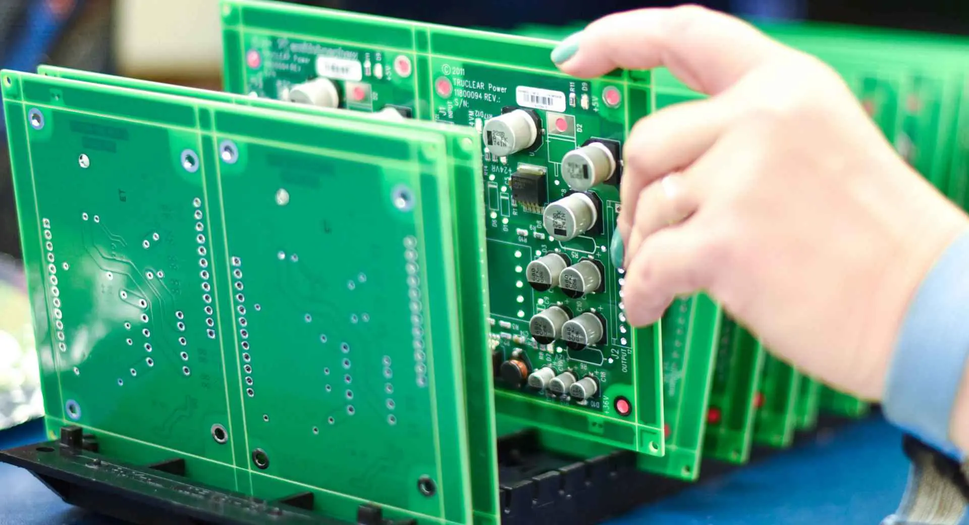
All about TACONIC material RF-35 PCB Manufacturing

taconic laminates

Introduction

Taconic RF-35 is a popular high frequency laminate material designed for performance-driven RF PCB applications. With a dielectric constant of 3.5, low loss, and tight material uniformity, RF-35 enables excellent signal integrity for today’s high speed digital and analog circuits.

This article provides an in-depth look at RF-35 material properties, performance capabilities, design considerations, and applications. We’ll explore everything engineers need to know about specifying and working with this versatile RF material.

RF-35 Overview

Taconic RF-35 is a PTFE composite laminate comprised of:

  • Woven fiberglass reinforcement
  • Ceramic filler particles
  • PTFE (polytetrafluoroethylene) resin system

With a dielectric constant of 3.5, it provides:

  • Excellent high frequency signal performance
  • Very low loss characteristics
  • Tight dielectric constant tolerance

RF-35’s properties make it suitable for a wide range of radio frequency, microwave, millimeter-wave, and multi-gigabit digital applications. It strikes an optimal balance between cost and high frequency signal integrity.

Some key traits of Taconic RF-35 include:

  • Dielectric constant of 3.5 +/- 0.05
  • Low loss with tight uniformity
  • Excellent thermal stability
  • Good CTE for reliability
  • Lead-free compatible
  • US laminator source
  • ITAR free
  • RoHS compliant
  • Cost-effectiveness

For designs from 10+ Gbps digital to Ku band RF, RF-35 delivers proven results across countless commercial and defense programs.

Material Properties

RF-35 is formulated from PTFE reinforced with ceramic particles to achieve:

Dielectric Constant – The k-value determines velocity of signal propagation and affects many circuit parameters. RF-35 provides an Er of 3.5 with very tight +/- 0.05 tolerance for consistent performance. This enables excellent impedance control compared to typical FR-4 (Er=4.5).

Loss Tangent – With a loss tangent of just 0.0019, RF-35 provides very low loss for high frequency energy. This maximizes Q factors in resonant circuits and insertion loss in transmission lines. Wide range of tested Dk from DC to Ku band.

Moisture Absorption – At just 0.02% moisture absorption, RF-35 resists detrimental effects of humidity and water ingress far better than conventional FR-4 material. This enhances long term reliability.

Thermal Performance – With a Z-axis CTE of 82 ppm/C, close PCB/laminate CTE matching reduces stresses under temperature cycling for excellent reliability. Good thermal conductivity (0.71 W/mK) spreads heat.

Lead-Free Assembly – RF-35 achieves high Tg (>280C) allowing compatibility with lead-free solder profiles of up to 260C for modern assembly.
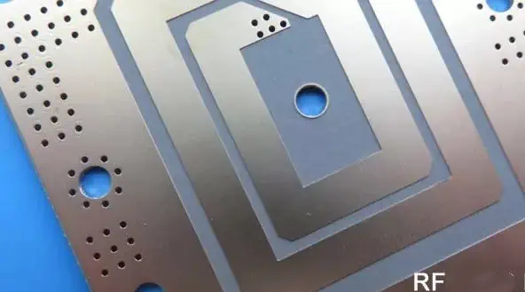
Available Forms

RF-35 laminate allows flexibility through different standard offerings:

Copper Cladding

  • 1⁄2, 1, and 2 oz ED copper foil
  • Standard HTE copper and rolled copper available
  • Double-sided cladding enables signal layers
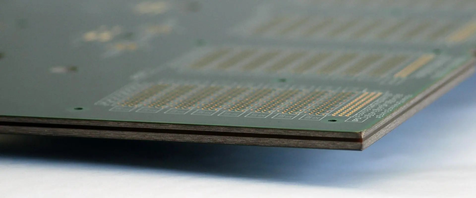
Core Thicknesses

  • From 0.005 inches to 0.125 inches
  • Typical stackups use multiple 0.005″ cores
  • Thicker cores provide rigidity when needed

Panel Sizes

  • 18” x 24”, 18” x 36”, and 24” x 36” standard panels
  • Custom panel sizes possible

Prepreg

  • 106 and 1067 styles available
  • Enables bonding multilayer board stackups
  • Matching resin system

Rod and Plate

  • For machined parts, spacers, and non-PCB applications
  • Reduces PIM in RF assemblies
  • Ideal for fixtures and testing

This range covers the needs of most RF-35 PCB implementations from prototyping to production.

PCB Performance Capabilities

Taconic RF-60TC PCB

RF-35 laminate provides excellent RF and high speed digital performance when designed properly:

Frequency Range

  • Usable continuous range from DC to Ku band (18 GHz)
  • Material characterizations up to 40+ GHz
  • Q factors exceeding 300 above 8 GHz

Loss

  • Low loss tangent of 0.0019
  • Insertion loss < 0.016 dB/inch at 20 GHz in 50Ω stripline

VSWR

  • Tight dielectric constant tolerance enables excellent impedance control
  • VSWR < 1.2 up to 15 GHz achievable

Propagation Delay

  • Delay = 1.7 ns/inch typical at 50Ω
  • Enables high data rates and rise time performance

Pulse Response

  • TDR shows minimal discontinuities and reflections
  • Clean time domain performance for ultra high-speed digital

Leveraging these attributes allows RF-35 PCBs to deliver highly repeatable RF and high speed digital operation.

Design Considerations

To obtain maximum benefit from RF-35 laminates, engineers should follow best design practices:

Stackup Planning

  • Use multiple thinner cores instead of one thick core
  • Alternating grain direction improves dimensional stability
  • Model expected performance in solver

Impedance Control

  • Leverage precise Er of 3.5 to maintain target impedance
  • 50Ω striplines for RF and high-speed routing
  • Controlled line width, dielectric height, trace geometry

Skin Effect

  • Consider skin effect depth above ~ 8-10 GHz
  • Utilize surface treatments like micro-etching

Signal Coupling

  • Careful gap/spacing rules between traces
  • Ground plane isolation techniques
  • Avoid 90 ̊ bends; use arc/tapered geometries

Thermal Management

  • Ensure sufficient thermal ground plane spreading
  • Efficient component layout to avoid hotspots
  • Consider thermal vias for heat transfer

Paying attention to these guidelines helps achieve first-pass PCB layout success with RF-35.

Recommended Stackups

Typical RF-35 PCB stackups may use configurations like:

Show Image

  • Multiple thin dielectric cores
  • Signal routing on surface layers
  • Dedicated ground planes near signals
  • Buried capacitance within stackup
  • Component cavities in ground planes

The thin cores and smooth copper foils of RF-35 enable tight impedance tolerance and high performance interconnects between ICs, filters, amplifiers, control logic, and other components.

Benefits vs. FR4

Compared to conventional FR-4 laminates, RF-35 provides:

Superior Loss Characteristics

  • Lower loss tangent: 0.0019 vs 0.02 for FR-4
  • Much flatter loss vs. frequency curve
  • Maintains low loss to > 10 GHz

Tighter Dielectric Constant Tolerance

  • Tolerance +/- 0.05 vs +/- 0.25 for FR-4
  • Enables consistent impedance across PCBs

Improved Moisture Resistance

  • 0.02% moisture absorption vs 0.2% for FR-4
  • Far less susceptible to humidity effects

Higher Frequency Support

  • Usable range to Ku band vs drop-off around 5 GHz with FR-4
  • Significantly better Q factors at high microwave bands

For peak signal integrity at microwave and mmWave frequencies, RF-35 is a clear choice over FR-4 material.

Typical RF-35 Applications

The capabilities of RF-35 make it a frequent choice for products including:

  • Satellite communications
  • Radar and remote sensing
  • 5G telecom infrastructure
  • Automotive radar
  • Wireless networking
  • Microwave radio/links
  • Defense electronics
  • Mobile devices
  • High speed digital design
  • Aerospace and avionics

Any application where optimizing signal integrity, reducing loss, and maintaining consistent performance over frequency are critical requirements will benefit from RF-35 PCB material.

Pros and Cons

Like any material, RF-35 has both advantages and disadvantages:

Pros

  • Excellent high frequency signal integrity
  • Low loss PTFE material
  • Tight dielectric constant tolerance
  • Lead-free assembly compatible
  • Good thermal conductivity
  • Reduced moisture absorption

Cons

  • Higher cost than FR-4
  • Lower flexural strength than glass-reinforced laminates
  • Requires advanced fabrication processes
  • Limited global supply chain

Conclusion

With its precise dielectric constant of 3.5 and low loss PTFE composition, Taconic RF-35 delivers proven performance for today’s emerging RF, microwave, and multi-gigabit digital designs. When engineered properly, RF-35 PCBs provide consistent behavior across fabrication lots and excellent high frequency response. For designers pursuing every last dB of loss or GHz of bandwidth, RF-35 remains an enabling material.

Frequently Asked Questions

Q: What are the key differences between RF-35 and common FR-4 laminates?

A: RF-35 provides much lower loss, tighter dielectric tolerance, lower moisture absorption, and extended high frequency range versus economical FR-4.

Q: What are some tips for working with thinner RF-35 cores?

A: Use dedicated layer alignment equipment, employ smaller component sizes, plan sufficient panelization spacing, and minimize handling to avoid cracking thin cores.

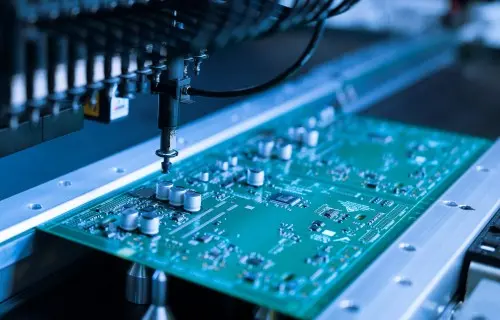
Q: Does RF-35 require special PCB fabrication processes?

A: RF-35 benefits from advanced PTFE processes for via formation, hole walls, and drilling. It also requires lamination processes tailored to thinner cores.

Q: What are typical finished RF-35 PCB thicknesses?

A: High frequency designs aim for overall PCB thickness under 0.030 inches. This requires precision lamination of multiple 0.005 inch dielectric cores.

Q: Are there lead-free soldering implications with RF-35 material?

A: RF-35 achieves high Tg (>280C) for compatibility with lead-free profiles up to 260C peak temperatures. Thermal relief in multilayers is recommended.

Do you know RF-35 (TACONIC material)?

RF-35(TACONIC material)

Performance:

(1) low cost;

(2) Excellent peel strength;

(3) Extraordinary low loss factor;

(4) low water absorption rate;

(5) Enhanced surface smoothness.

Application:

(1) power amplifier;

(2) filters and connectors;

(3) Passive components.

1)RF-35 is an organic-ceramic laminate material in the ORCER of TACONIC products.

2)It is a reinforced glass material based on woven glass cloth, and a combination of TACONIC’s ceramic filling technology and glass fiber coated PTFE technology.

3)RF-35 is the best choice for low cost, high volume commercial microwave and wireless frequency applications.

3)RF-35 of 1/20Z and 10Z copper foil boards, even with standard epoxy materials, have excellent peel strength and provide rework at any time.

4)The glass transition temperature of RF -35 exceeds 315 ℃.

5)The ultra-low water absorption and low loss factor of RF-35 minimizes phase shift in the frequency range of use.

6)The dimensional stability of RF-35 is due to the use of woven glass cloth in its design development.

7)RF-35 laminate material, generally with single or double-sided 1/20Z, 10Z and 20Z thickness of electrolytic copper foil. Different sizes of sheets can be selected according to requirements.

8)For the RF-35 microwave material, the relationship between the thermal expansion rate in the Z-axis direction and the temperature is shown in the figure below:

RF-35(TACONIC brand)

9)RF-35 dielectric constant changes with temperature:

PCB TACONIC brand material

10)RF-35 dielectric loss changes with temperature:

PCB RF-35 material

10)The relationship between the dielectric constant and frequency of RF-35 microwave materials is shown in the figure below:

Special PCB material

11)The relationship between the dielectric loss of RF and the frequency of microwave materials is shown in the figure below:

R35 TACONIC material

What is the difference between FFC connector and FPC connector ?

one layer flex pcb board

What is ffc wiring and what is  fpc wiring ?

Wiring, also known as flexible circuit board (FPC). It is used for the transmission of data within the active parts and areas, such as the hard disk connected to the mainboard of the computer, the data line of the optical drive, the data line of the mobile phone motherboard connected to the display screen, and so on. There are also connected devices between the data lines are collectively known as wiring. Wire layout is mainly divided into two kinds of round head (R-FFC for direct welding) and flat ends (for short FFC, for socket insertion). Most suitable for data transmission cables between moving parts and motherboards, between board and board, and for miniaturized electrical equipment. Because the price of FFC cable is better than that of FPC (flexible Printing Circuit), its application will become more and more extensive. In most places where FPC is used, you can basically replace it with FFC.

https://www.youtube.com/watch?v=pG2FsS7ZXuo
FPC

Wiring characteristics

  1. The wire layout is small, light weight, the original design of the wiring board is used to replace the larger wire harness wire. Wiring is usually the only solution to miniaturization and mobility on the current cut TIng-edge assembly board. Wire placement (sometimes referred to as flexible printed circuit) is the etching of copper circuit or printed polymer thick film circuit on the polymer substrate. For thin, light, compact and complex devices, the design solutions range from single-sided conductive circuits to complex multi-layer three-dimensional prototype pcb assembly. The total weight and volume of wire arrangement is 70% less than the traditional round wire harness method. Wire placement can also increase strength by using reinforced materials or linings to achieve additional mechanical stability.
  2. Wire placement can be moved, bent, twisted without damaging the wire, and can conform to different shapes and special package sizes. The only limitation is the volume space problem. Because it can withstand millions of times of dynamic bending, wiring can be well applied to continuous or periodic motion of the internal system, as part of the final product function. The solder joints on the rigid PCB are subjected to thermal mechanical stresses that fail after hundreds of cycles. “require electrical signals / power to move,” said Jenny, a product manager at EECX. Some products with smaller shape coefficients / package sizes benefit from wire placement.
long FPC board

3, wiring has excellent electrical properties and dielectric properties,” said the CEO of heat-resistant. LT Electronic. “low dielectric constants allow electrical signals to be transmitted quickly; Good thermal properties make the element easy to cool down; higher glass conversion temperature or melting point make the element work well at higher temperature.

4, wiring has higher assembly reliability and quality. Wiring reduces the hardware required for internal wiring, such as solder joints, trunk wires, backboard lines and cables commonly used in traditional electronic packaging, enabling wiring to provide higher assembly reliability and quality. Ping.Wu, a marketing manager with a higher misalignment rate of electronic components, said Ping.Wu, a marketing manager of. EECX Electronic Products Division, a market manager with complex multiple systems, said, “the stiffness of wiring is low and the size is small,” said Ping.Wu, the market manager of. EECX Electronic Products Division, which is composed of complex multiple systems. It is precisely because of the small size of the wiring board components, so the use of less material. ” With the emergence of quality engineering, a thin flexible system is designed to be assembled in only one way, thus eliminating many human errors usually associated with independent wiring engineering.

What is FFC wiring

FFC wiring is also called flexible flat cable, which can choose the number and spacing of wire arbitrarily, make the wire more convenient, greatly reduce the volume of electronic products, reduce production cost, improve production efficiency, and is most suitable for moving parts and motherboards. PCB board is used for data transmission cable between PCB boards and miniaturized electrical equipment. The common specifications are 0.5mm / 0.8mm / 1.0mm / 1.25mm / 1.27mm / 1.5mm / 2.0mm / 2.54mm and so on.

long fpc

Line arrangement difference between FFC and FPC

FPC is the Flexible Printed Circuit flexible printed circuit, and in terms of their manufacturing, they are formed in a different way:

1, FPC is a kind of flexible circuit board with different single and double sides and multilayer pcb structure, which is treated by FCCL (flexible copper foil) by chemical etching.

2, FFC is made of flat copper foil with upper and lower layers of insulating foil film, the finished product is simple and the thickness is thicker.

FPC

What is ENEPIG Plating Finish in PCBs?

ENEPIG pcb

Introduction

Printed circuit boards (PCBs) serve as the core component in virtually every electronic device. They provide the substrate to mount and interconnect electronic components using copper traces. To protect these copper traces from corrosion and ensure reliable solder joints, the copper pads are plated with solderable surface finishes.

ENEPIG (Electroless Nickel Electroless Palladium Immersion Gold) has emerged as an advanced plating finish for PCBs, providing excellent solderability while also resisting corrosion. This article provides a comprehensive understanding of ENEPIG plating technology, its properties, process steps, pros and cons, and applications.

YouTube video

What is ENEPIG Plating?

ENEPIG PCB

ENEPIG or electroless nickel electroless palladium immersion gold plating is a PCB surface finish comprising of three metal platings deposited sequentially on copper pads – nickel, palladium and gold.

  • Electroless nickel – Corrosion resistant layer
  • Electroless palladium – Barrier layer prevents nickel diffusion
  • Immersion gold – Outermost layer provides solderability

The term ‘electroless’ refers to autocatalytic deposition without using electrical current. The metals deposit through a chemical reduction reaction. ‘Immersion’ uses a chemical displacement reaction.

This tri-metal finish provides excellent solderability while also resisting corrosion and oxidation. It is an alternative to conventional finishes like electrolytic nickel/gold, immersion tin and OSP (Organic Solderability Preservatives).

Key Properties

  • Excellent solderability and wettability
  • Low and stable contact resistance
  • Corrosion resistance comparable to gold
  • Good wirebondability
  • Lead-free solder compatibility
  • Halogen-free formulation available

Why Use ENEPIG Plating?

Advantages of ENEPIG

ENEPIG plating offers following benefits over other PCB finishes:

1. Reliable Solderability

  • Gold outer layer provides excellent solderability, similar to immersion gold.
  • The underlying nickel and palladium enhance adhesion of the gold layer.

2. Lead-free Solder Compatibility

  • Gold allows reliable lead-free soldering, unlike tin finishes which are prone to tin whiskers.
  • Palladium barrier layer prevents diffusion of nickel into solder joint.

3. Corrosion Resistance

  • The nickel underlayer provides corrosion resistance comparable to gold.
  • Palladium isolates the nickel from the solder joint.

4. Halogen-free Formulations

  • Electroless nickel and palladium use halogen-free chemistries, avoiding issues with immersion gold.

5. Contact Resistance Stability

  • The nickel and palladium base preserves the low contact resistance of gold finishes.

6. Wire Bond Compatibility

7. Self-Limiting Thickness

  • Immersion plating process provides self-limited uniform thickness.

ENEPIG Plating Process Steps

The Features Between ENIG and ENEPIG

ENEPIG finish deposition involves sequential electroless plating of nickel, palladium and immersion gold:

1. Electroless Nickel Plating

  • PCB undergoes dilute acid cleaning and microetching.
  • Activated in palladium chloride to initiate nickel deposition.
  • Electroless nickel plating solution deposits nickel through an autocatalytic chemical reaction.
  • Thickness of 5 to 8 micro-inches nickel is plated.

2. Electroless Palladium Plating

  • Nickel layer is activated in an acidic solution.
  • Electroless palladium solution deposits a thin layer of palladium, typically 0.2 to 0.5 micro-inches.
  • Palladium prevents diffusion of nickel into solder joint.

3. Immersion Gold Plating

  • PCBs are dipped in immersion gold solution which contains gold salts.
  • The gold displaces palladium through a galvanic exchange reaction.
  • Gold layer of 0.1 to 0.5 micro-inches is plated.
  • Provides solderability and wire bondability.

Comparison of ENEPIG vs Other Finishes

ENEPIG and ENIG
ENEPIG and ENIG
ParametersENEPIGENIGImm. TinOSP
SolderabilityExcellentExcellentGoodFair
Process ControlModerateDifficultEasyEasy
Lead-free solder compatibleYesYesProne to whiskersYes
Corrosion resistanceExcellentModeratePoorFair
Contact resistanceLow and stableUnstableLowModerate
Shelf life12 months6-9 months4-6 months3-6 months
Soldering heat resistanceGoodFairExcellentPoor
Wirebond compatibilityExcellentExcellentFairPoor
CostModerateHighLowVery low

Pros and Cons of ENEPIG Finish

Pros:

  • Excellent solderability and contact reliability
  • Resists corrosion as effectively as gold
  • Compatible with lead-free solders
  • Allows wire bonding
  • Provides stable low contact resistance
  • Halogen-free formulations available
  • Self-limiting and uniform thickness

Cons:

  • More expensive than tin, silver, OSP finishes
  • Requires precise process control
  • Palladium is expensive
  • Multiple plating steps increase cycle time
  • Shelf life shorter than tin finishes

Applications of ENEPIG Plating

The key applications where ENEPIG finish provides benefits are:

1. Lead-free Soldering

Compatible with lead-free solders, unlike tin finishes prone to whiskering.

2. Automotive Electronics

Withstands under-hood temperatures. Halogen-free for reduced outgassing.

3. Avionics and Aerospace

High reliability needed for extreme conditions.

4. Medical Electronics

Biocompatible finish.

5. Wireless and Portable Electronics

Supports lead-free soldering and tin whisker mitigation.

6. High Speed Digital Circuits

Gold provides low contact resistance stability.

7. Wire Bonding

The gold layer enables wire bonding.

ENEPIG Plating on Different PCB Pad Types

ENEPIG can be deposited on various finishes present on PCB pads:

Pad TypeProcess
Bare CopperDirectly applies ENEPIG finish
Immersion TinPre-activates with palladium before ENEPIG
Immersion SilverMasks pad surface before ENEPIG deposition
OSPRemoves OSP completely prior to ENEPIG
Electrolytic Nickel GoldStrips nickel and activates for ENEPIG process
Immersion GoldStrips gold, activates nickel, then follows ENEPIG steps
Solder Mask DefinedSelectively strip solder mask before plating ENEPIG

Key Process Challenges with ENEPIG

Some process challenges associated with ENEPIG plating include:

  • Uniformity: Electroless deposition depends on local chemical conditions. Careful monitoring and tank agitation is required.
  • Palladium Activation: Insufficient activation can cause non-uniform nickel deposition and gold embrittlement.
  • Bath Maintenance: Regular analysis and replenishment of electroless baths is critical.
  • Solder Mask Adhesion: Compatibility between solder mask and ENEPIG chemistry must be ensured.
  • Via Filling: Deposits thin coating only. For thicker coatings, additional electroless copper buildup may be required.

Frequently Asked Questions (FAQs)

Q1. Does ENEPIG finish contain any nickel on the surface?

No. The top surface is pure gold, with palladium and nickel below it. Palladium acts as diffusion barrier to isolate nickel from gold layer.

Q2. Can ENEPIG finish withstand multiple reflow cycles?

Yes, ENEPIG provides excellent soldering heat resistance. The underlying nickel and palladium enhance adhesion of the gold layer through repeated temperature cycling.

Q3. What is the typical thickness of ENEPIG finish?

Thickness values are: Nickel: 5-8 microinches, Palladium: 0.2-0.5 microinches, Gold: 0.1-0.5 microinches. Total thickness is usually under 1 micron.

Q4. Does ENEPIG allow both lead and lead-free soldering?

Yes, the gold outer layer of ENEPIG is highly solderable with both lead-based and lead-free solders. Underlying nickel and palladium enhance intermetallic formation.

Q5. Can ENEPIG finish withstand board assembly in wave soldering?

ENEPIG finish has adequate thermal resistance to withstand wave soldering processes, unlike PCB finishes like OSP which have poor heat resistance.

What’s the Difference Between SMD and NSMD in BGA Footprint?

surface mount pcb assembly

Correct PCB pad design is crucial to effectively weld components to the circuit board. For bare pad  prototype pcb assembly , there are two common welding methods — SMD (Solder Mask Defined) and NSMD (Non-Solder Mask Defined), each with its own characteristics and advantages.

The Difference Between SMD and NSMD

SMD:

SMD refers to the resistance layer opening is less than the metal pad welding process. This process reduces the possibility of the welding plate falling off during welding or dewelding. However, the disadvantage is that the method reduces the copper surface area that can be used for solder joint connections and reduces the space between adjacent pads. This limits the thickness of the trace lines between the pads and may affect the use of through-hole.

NSMD:

NSMD refers to the welding plate process in which the opening of the resistance layer is larger than that of the welding plate. This process provides greater surface area for solder joint connections and greater clearance between solder pads (compared to SMD), allows for wider line width and more through-hole flexibility, but NSMD pads are more likely to fall off during welding and disassembly. Even so, NSMD still has a better welding firm performance and is suitable for solder joint sealing pads.

Introduction

Ball grid array (BGA) packages are widely used for integrated circuits as they provide a high density of interconnections beneath the package. BGA packages connect to the PCB through an array of solder balls that serve as the leads. When defining the PCB land patterns or footprint for the BGA package, the solder mask design requires special consideration for reliability. The solder mask can either cover the copper pad completely, known as solder mask defined (SMD), or have openings larger than the pad diameter, called non-solder mask defined (NSMD).

This article explains what SMD and NSMD BGA footprints are, their differences, key design considerations, assembly process impacts and applications.

Solder Mask Defined (SMD) BGA Footprints

YouTube video

In an SMD BGA footprint, the openings in the solder mask layer fully cover and intersect the underlying copper pads. This results in the solder mask itself defining the final land dimensions and controlling the volume of solder paste printed. Hence the name solder mask defined (SMD) footprint.

With SMD footprint, the copper pad size is typically 20 to 60 μm greater than the solder mask opening based on registration tolerances. The key characteristics of SMD BGA land patterns are:

  • Solder mask opening equals the intended land diameter for the BGA balls. This controls the amount of solder.
  • Excellent registration is needed between layers to keep the pad centered in the mask opening.
  • The pad shape is not critical and there is no risk of exposed copper.
  • Allows smaller pad and pitch dimensions since solder mask dams prevent bridge formation.
  • Solder voiding can occur more easily due to smaller paste volumes.

Here is an illustration of solder mask defined (SMD) BGA footprint:

The tight alignment between copper pad and solder mask opening required for SMD footprint necessitates use of the tightest manufacturing tolerances.

Non-Solder Mask Defined (NSMD) BGA Footprints

In a non-solder mask defined (NSMD) footprint, the openings in the solder mask layer are larger than the diameter of the copper pads. This exposes the entire copper pad allowing the pad size and shape to define the final land dimensions rather than the solder mask.

In NSMD footprint, the mask openings exceed the copper pad size by at least 150 μm based on registration tolerances. Key features are:

  • The pad diameter determines the solder volume. Solder mask does not restrict soldering.
  • Requires greater clearance between pads to prevent mask bridging since mask does not dam solder flow.
  • Copper pad can be dog-bone or dumbbell shaped to allow solder filleting.
  • Pad registration to mask opening is non-critical. Mask just needs to expose pad.
  • Allows larger paste deposit area so less prone to solder voids.

Here is an illustration of non-solder mask defined (NSMD) footprint:

The NSMD design provides more tolerance for pad positioning within the mask opening but demands greater spacing between adjacent pads.

Comparison Between SMD and NSMD Footprints

Here is a summary comparison of some key differences between the solder mask defined (SMD) and non-solder mask defined (NSMD) footprints for BGA packages:

ParameterSMD FootprintNSMD Footprint
Mask opening vs. padEqual to pad diameterAt least 150 μm greater than pad
Solder volume controlDefined by mask openingDefined by pad diameter
Pad shapeLimited by mask openingCan use dogbone, dumbbell shapes
bridging riskLower – mask dams prevent solder spreadHigher – no mask dams so needs more spacing
Registration needsTight mask to pad registration essentialPad registration non-critical
Solder voidingHigher risk due to small volumesLower risk thanks to larger paste deposits
Design and assembly costGenerally higherLower cost

In summary, SMD design works best for fine pitch parts where the solder mask yields precise solder volumes, while NSMD is preferable for larger packages needing greater process and registration tolerances.

SMD Footprint Design Guidelines

When designing an SMD footprint for a BGA package, here are some guidelines to follow:

  • Pad diameter should be 20 to 60 μm less than mask opening based on registration capabilities
  • A minimum web of 50 to 75 μm is required between adjacent mask openings
  • Laser cut mechanically drilled (LCMD) vias can be placed within pad area if space is tight
  • 1:1 pad to ball ratio should be used for perimeter balls
  • Non-perimeter pads can utilize area array patterns to increase routing space
  • Pad shapes are largely non-critical since mask controls shape and volume
  • Thermal reliefs in pad are not beneficial due to small paste volumes
  • For dense footprint, use tighter mask to pad tolerances for web reduction
  • Reduce pad spacing further by shifting adjacent rows/columns by 50% pitch
  • Use thicker mask of at least 150 μm to prevent tacky solder damage

NSMD Footprint Design Guidelines

For non-solder mask defined BGA footprints, following guidelines are recommended:

  • Pad diameter should be smaller than mask opening by at least 150 μm
  • Minimum web of 225 μm should be kept between mask openings
  • Dogbone, dumbbell pad shapes can be used to improve solder filleting
  • LCMD vias must be placed clear of extended pad edges
  • 1:1 pad assignment preferred on package perimeter
  • Thermal reliefs can be incorporated in pad shapes
  • Increased spacing required between pads due to lack of solder dams
  • Thinner solder mask down to 75 μm can suffice if bridging risks are low
  • Tighter mask to pad registration not needed allowing faster assembly
  • Can shift adjacent rows/columns by 25% pitch only due to bridging risks
  • Suitable for footprint sizes above 15mm × 15mm

Assembly Process Impacts

The choice between SMD or NSMD footprints for a BGA package influences various aspects of the assembly process:

Stencil Design

For SMD pads, stencil openings equal the pad size as mask defines shape. For NSMD pads, stencil openings must be smaller than pad area to control solder volume.

Solder Paste Printing

NSMD pads allow larger print deposits reducing voids. SMD pads need tighter print process control to prevent solder balls.

Pad Tolerance Changes

SMD needs tight mask to pad registration. NSMD relaxes this requirement allowing cheaper PCB fabrication.

Spacing and Routing

NSMD needs more clearance between pads forcing larger pitch. This consumes more PCB area but eases routing.

Voiding Risks

The smaller paste deposits of SMD make it more prone to voids versus NSMD pads.

Bridging Risks

Lack of mask dams means NSMD has higher bridging risks requiring careful paste volume control.

Fillet Formation

NSMD allows pad shapes to improve solder side filleting. SMD shape is restricted by mask aperture.

Rework Concerns

SMD pads limit where heat can be applied during rework. Mask restricts access to NSMD pads less.

SMD vs NSMD Applications

SMD footprints are preferred for:

  • Fine pitch BGA packages ≤ 0.8mm pitch
  • Small BGAs with pitch ≤ 0.5mm
  • Packages with high pin counts
  • Portable consumer electronics where space is critical

NSMD footprints suit:

  • Lower density BGA packages with >1mm pitch
  • Larger package sizes above 15mm x 15mm
  • Automotive grade parts needing greater process tolerances
  • Corner ball cases requiring dogbone pads for sufficient solder volume
  • Boards with fewer routing layers where pad spacing is less critical
  • Applications where solder voiding risks need minimization

Summary

In summary, solder mask defined (SMD) BGA footprints provide precision solder control by limiting paste volumes but demand tight fabrication tolerances. Non-solder mask defined (NSMD) pads relax tolerances but occupy more space on the PCB unless carefully designed. Making the right choice based on pitch, pad count, size constraints and process capabilities is key to designing a reliable and manufacturable BGA footprint.

FAQs

Can SMD or NSMD be used for any BGA pitch?

SMD is preferred for fine pitch below 0.65mm due to solder control. NSMD is unsuitable below 0.5mm because of bridging risks from lack of dams.

Which provides better resistance to shock and vibration?

NSMD allows larger fillets so can withstand mechanical stresses better. SMD may crack more easily at the package edges and corners.

Is NSMD also called extended pad in some datasheets?

Yes, extended pad is another term used to indicate NSMD footprint where pad extends beyond the solder mask opening.

Does NSMD increase the risk of thermomechanical fatigue?

Slightly – the larger pad size leads to higher shear stresses at the pad periphery which must be considered in reliability testing.

Can thermal vias be incorporated in BGA pads?

For SMD pads thermal vias will reduce solder volume further increasing void risks. In NSMD thermal vias can be safely placed provided they do not infringe on the extended pad area.

PCB vs PCBA: Understanding the Key Differences and Applications

pcb vs pcba

Introduction

In today’s world, electronics are marvels of engineering, combining intricate components to create devices with incredible capabilities. At the heart of this technological revolution lie two crucial elements: Printed Circuit Boards (PCBs) and Printed Circuit Board Assemblies (PCBAs). These unsung heroes form the backbone of modern electronic devices, enabling the powerful performance we’ve come to expect.

For anyone working in the electronics field – whether you’re an engineer, designer, or manufacturer – understanding the differences between PCBs and PCBAs is more than just helpful; it’s essential. This knowledge is the key to making informed decisions when developing new products or improving existing ones.

YouTube video

This guide aims to demystify PCBs and PCBAs, exploring their core characteristics, various types, cutting-edge manufacturing techniques, and unique features. By delving into these topics, we’ll equip you with the insights needed to take your electronic projects to the next level.

As we explore the world of PCBs and PCBAs, you’ll gain valuable knowledge that will help you push the boundaries of what’s possible in electronics. Whether you’re a seasoned professional or just starting in the field, this guide will provide you with the tools to innovate and excel in your work.

What is a PCB?

A Printed Circuit Board (PCB) is the unsung hero of modern electronics. Imagine it as a thin, flat canvas made of insulating materials like fiberglass or epoxy resin. This canvas is adorned with intricate patterns of conductive copper traces, creating a masterpiece of electronic connectivity.

At its core, a PCB serves as a sturdy foundation for electronic components. It’s where resistors, capacitors, and integrated circuits come together to form a harmonious circuit. These components are securely attached to the board, working in concert to bring your electronic device to life.

PCBs are game-changers in electronics design for several reasons:

  1. Simplification: They transform complex wiring into neat, organized pathways.
  2. Reliability: By providing a stable platform, PCBs enhance device dependability.
  3. Compact Design: PCBs enable the creation of sleek, high-performance circuits.
  4. Easy Troubleshooting: Their organized layout makes identifying and fixing issues a breeze.
  5. Physical Support: PCBs act as a protective scaffold, keeping components aligned and secure, even in harsh conditions.

The performance of a PCB is influenced by various factors:

  • The type and thickness of the insulating material
  • The width and spacing of conductive traces
  • The quality of solder joints

These elements shape the board’s electrical properties, such as resistance, capacitance, and inductance, which in turn affect the overall device performance.

Designing an effective PCB is both an art and a science. It requires careful consideration of these factors to ensure the board – and the device it powers – performs at its best. Whether you’re creating a smartphone or a satellite, the humble PCB is what brings your electronic vision to life.

Types of PCBs and Their Main Components

4 Layer Fr4 3oz 1.0mm ENIG PCB

PCBs come in various types, each designed to meet specific needs in the world of electronics. Let’s explore the main types and then dive into the key components that make up these technological marvels.

Types of PCBs

  1. Single-sided PCBs
    • The simplest and most cost-effective option
    • One conductive layer on a single side of the insulating material
    • Ideal for basic electronics and simple control systems
    • Components attached via through-hole or surface-mount techniques
  2. Double-sided PCBs
    • Conductive traces on both sides of the board
    • Allows for more complex circuits and higher component density
    • Uses plated-through holes (PTHs) or vias for inter-layer connections
    • Common in automotive electronics, industrial controls, and communication devices
    • More versatile but slightly more expensive than single-sided PCBs
  3. Multilayer PCBs
    • Multiple layers of conductive and insulating materials
    • Can have 4 to 30+ layers
    • Uses PTHs, blind, and buried vias for inter-layer connections
    • Ideal for high-performance electronics like advanced computers and medical devices
    • Offers superior performance and space efficiency but at a higher cost

Main Components of a PCB

  1. Substrate (FR4)
    • The foundation of the PCB, typically made of fiberglass
    • Provides mechanical support and insulation
  2. Copper Layers
    • Thin sheets of copper laminated to the substrate
    • Form the conductive pathways for electrical signals
  3. Solder Mask
    • Protective layer applied over the copper
    • Usually green, but can come in various colors
    • Prevents short circuits and protects copper from external factors
  4. Silkscreen
    • Typically white layer containing text and symbols
    • Serves as a guide for component placement and orientation
  5. Edge Connectors (Gold Fingers)
    • Gold-plated terminals on the board’s edge
    • Used for interfacing with other boards or devices
  6. Vias
    • Small holes drilled through the PCB
    • Enable electrical connections between different copper layers

Choosing the right PCB type depends on factors like circuit complexity, available space, performance requirements, and budget. Understanding these PCB types and components empowers designers and engineers to make informed decisions, creating electronics that push the boundaries of what’s possible.

Whether you’re working on a simple gadget or a cutting-edge device, the right PCB can make all the difference. By mastering the intricacies of PCB types and components, you’re well-equipped to tackle any electronic challenge that comes your way.

PCB Manufacturing Process: From Design to Reality

Creating a Printed Circuit Board (PCB) is like orchestrating a symphony of precision and technology. Let’s break down this fascinating process into three main acts: Design, Fabrication, and Assembly.

  1. Design: Blueprinting the Future

The journey begins in the digital realm, where Computer-Aided Design (CAD) software becomes the artist’s canvas. Here’s what happens:

  • Engineers map out component layouts and trace routes
  • They strategically place vias and plated-through holes (PTHs)
  • Materials are selected, layer structures are planned, and trace dimensions are defined
  • The final design is exported as Gerber files, the universal language of PCB manufacturing
  1. Fabrication: Bringing the Design to Life

This is where the magic happens, transforming digital designs into tangible boards:

  • Start with a copper-clad substrate (usually FR-4, a fiberglass-epoxy composite)
  • Etch the copper to create the designed trace patterns (chemically or mechanically)
  • For multilayer PCBs, individual layers are created and then fused with heat and pressure
  • Drill holes for component mounting and inter-layer connections
  • Plate the holes with copper to create PTHs and vias
  • Apply solder mask to protect the traces
  • Add silkscreen for component guidance and important information
  • Finish with surface treatments to prevent oxidation
  1. Assembly: Adding the Brains to the Board

Now it’s time to populate the PCB with electronic components:

  • Components are placed using one of two methods: a) Through-hole soldering: Component leads are inserted into pre-drilled holes and soldered b) Surface-mount technology (SMT): Components are soldered directly onto the board’s surface
  • Specialized machines precisely place components
  • Soldering techniques (like reflow or wave soldering) secure the components

Each step in this process is a delicate dance of precision and expertise. Understanding this journey helps engineers and designers make informed decisions to optimize performance, reduce costs, and enhance manufacturability.

From the initial concept to the final product, PCB manufacturing is a testament to human ingenuity and technological advancement. Whether you’re designing a simple gadget or a complex computing system, knowing these steps empowers you to create better, more efficient electronic devices.

Remember, in the world of PCBs, attention to detail isn’t just important—it’s everything!

What is a PCBA ?

Sweeping Robot PCBA

PCBA stands for Printed Circuit Board Assembly. It’s the result of attaching electronic components to a bare printed circuit board (PCB). This process transforms a simple PCB into a functional electronic circuit.

The PCB assembly process is crucial in manufacturing electronic devices. It involves carefully placing and soldering various components onto the board according to a specific design.

A PCBA serves as the foundation for electronic devices, allowing different components to work together efficiently. It ensures that the device functions as intended by:

  1. Guiding electrical signals between components
  2. Following the device’s schematic design
  3. Providing ground and voltage planes
  4. Maintaining proper impedance control for optimal electrical performance

The quality and performance of a PCBA depend on several factors:

  • The quality of the components used
  • The accuracy of the assembly process
  • The reliability of the solder joints

In essence, a PCBA is the heart of most electronic devices, enabling them to perform their intended functions.

PCBA Composition

A Printed Circuit Board Assembly (PCBA) is a complex yet unified electronic component. Here’s what makes up a PCBA:

  1. The PCB (Printed Circuit Board)

The PCB is the foundation of the PCBA. It’s a flat board made of laminate materials, often in multiple layers. The PCB provides:

  • Structural support
  • Conductive pathways for electrical signals
  1. Electronic Components

Various electronic parts are mounted on the PCB, including:

  • Passive components: resistors, capacitors, inductors
  • Active components: transistors, integrated circuits

Each component has a specific function, contributing to the overall performance of the device.

  1. Traces and Vias
  • Traces: Thin conductive paths on the PCB surface that carry electrical signals
  • Vias: Small holes connecting different layers in multi-layer PCBs, allowing signals to travel between layers
  1. Solder Paste

Solder paste is applied to the board before component placement. It consists of:

  • Fine solder particles
  • Flux

The paste ensures solid electrical and mechanical connections when heated. Proper application is crucial for the quality of the final assembly.

In summary, a PCBA is a carefully designed combination of these elements. Each part plays a vital role in creating a functional electronic circuit that powers our modern devices.

Two Main PCBA Assembly Methods

PCBA (Printed Circuit Board Assembly) refers to the process of attaching electronic components to a printed circuit board. There are two primary methods used in PCBA:

  1. Through-Hole Technology (THT)

THT is a traditional method of PCB assembly. Key features include:

  • Components have long leads inserted through holes in the PCB
  • Leads are soldered on the opposite side of the board
  • Provides strong mechanical and electrical connections

Applications of THT:

  • Aerospace equipment
  • Military hardware
  • Industrial machinery
  • Vintage electronics

THT Assembly Process: a) Drilling holes in the PCB b) Inserting component leads c) Soldering (often using wave soldering) d) Trimming excess leads and cleaning

  1. Surface-Mount Technology (SMT)

SMT is a more modern approach to PCB assembly. Key features include:

  • Components are mounted directly onto the PCB surface
  • Uses small solder pads instead of holes
  • Allows for smaller, more compact designs

Applications of SMT:

  • Smartphones
  • Tablets
  • Wearable devices

SMT Assembly Process: a) Applying solder paste using a stencil b) Placing components with pick-and-place machines c) Reflow soldering in a specialized oven d) Inspection and quality control (often using Automated Optical Inspection)

Both methods have their advantages and are chosen based on the specific requirements of the electronic device being manufactured.

PCBA Testing: Ensuring Quality and Reliability

PCBA (Printed Circuit Board Assembly) testing is a crucial step in the manufacturing process, ensuring that assembled circuit boards meet quality standards and function as intended. This process involves checking various aspects such as IC programming, power, current, voltage, and circuit continuity.

Importance of PCBA Testing:

  • Critical quality control measure
  • Ensures product functionality and reliability
  • Helps prevent defective products from reaching customers

Main PCBA Test Types:

  1. In-Circuit Test (ICT)
    • Checks circuit functionality
    • Measures current and voltage values
    • Analyzes fluctuation curves, amplitude, and noise
  2. Functional Circuit Test (FCT)
    • Simulates real-world usage
    • Identifies hardware and software issues
    • Verifies overall product functionality
  3. Flying Probe Test
    • Uses moving probes for electrical testing
    • Examines component values and characteristics
    • Ideal for low-volume or prototype boards
  4. Aging Test
    • Continuous power-on testing
    • Simulates long-term use
    • Evaluates product durability and stability
  5. Environmental Stress Test
    • Exposes PCBAs to extreme conditions
    • Tests temperature, humidity, water resistance, drop, and vibration tolerance
    • Assesses overall product reliability

Choosing the right combination of tests depends on the specific product requirements and intended use. Experienced PCBA manufacturers can efficiently conduct these tests to ensure high-quality, durable products.

PCB vs. PCBA: Understanding the Distinctions

pcb-vs-pcba
pcb-vs-pcba

While PCB (Printed Circuit Board) and PCBA (Printed Circuit Board Assembly) are closely related, they have several key differences:

  1. Definition

PCB:

  • A bare board with conductive traces on a non-conductive substrate
  • Provides the foundation for electronic circuits

PCBA:

  • A fully assembled PCB with electronic components attached
  • A functional circuit ready for use in electronic devices
  1. Manufacturing Process

PCB:

  • Involves designing the layout
  • Creating conductive pathways through etching
  • Drilling holes for component insertion

PCBA:

  • Starts with a completed PCB
  • Adds components like resistors, capacitors, and integrated circuits
  • Involves processes such as:
    • Solder paste application
    • Component placement
    • Reflow soldering
  1. Cost Considerations

PCB:

  • Generally less expensive
  • Cost mainly includes materials and fabrication

PCBA:

  • More costly overall
  • Includes PCB cost, component costs, and assembly fees

Comparison Table:

AspectPCBPCBA
StateBare boardAssembled board
FunctionalityNon-functional on its ownFunctional electronic circuit
ComponentsNoneVarious electronic parts attached
ProductionDesign and fabrication onlyIncludes component placement and soldering
CostLowerHigher
UseIntermediate productFinal product or sub-assembly

Understanding these differences is crucial for anyone involved in electronics design, manufacturing, or procurement.

Choosing Between PCB and PCBA

When to Choose PCB:

  • Early stages of product design and prototyping
  • Testing and refining board layout
  • Evaluating conductive pathways
  • When you have in-house capability for component assembly
  • If you prefer flexibility for alterations

When to Choose PCBA:

  • Need for fully operational boards
  • Direct integration into products
  • Mass production scenarios
  • Time-saving solution
  • Ensuring consistency and reducing assembly errors
  • Cost-effective at scale
  • For finished products or near-final prototypes

Applications of PCB and PCBA:

  1. Consumer Electronics: Smartphones, TVs, etc.
  2. Automotive Electronics: EVs, battery management, autonomous navigation
  3. Industrial Controls: PLCs, motor drives, sensors
  4. Medical Devices: Heart rate monitors, MRI scanners, surgical instruments
  5. Computing Devices: Servers, laptops, hosting CPUs, GPUs, RAM
  6. Telecommunications: Routers, switches, base stations
  7. Aerospace and Defense: Cockpit instrumentation, missile guidance systems
  8. Internet of Things (IoT): Smart homes, wearables, industrial sensors

RAYMING PCB Services:

Company Highlights:

  • Focus on intelligent manufacturing for small and large-scale PCBA production
  • Swift service without compromising quality
  • In-house developed management systems (CRM, MES, ERP, IoT)
  • Expertise in various sectors: industrial control, smart home, instrumentation, vehicle IoT, communication power, medical devices, automotive, and aviation
  • Rigorous testing and prototype assembly protocols

RAYMING PCB positions itself as a partner for comprehensive PCB and PCBA solutions, from design to delivery, with a focus on innovation and quality across diverse industries.

What Cleaner Can I Use to Clean Circuit Board?

pcb clean

Printed circuit boards (PCB) need routine cleaning during manufacturing, rework and maintenance to remove contaminants like flux residues, dust, grease and other particles. Choosing the right circuit board cleaner is important to effectively remove contamination without damaging the board. This article discusses different types of PCB cleaners, how to select the appropriate one, cleaning methods and best practices.

Need for Cleaning Circuit Boards

the PCB with excess flux

Following are some key reasons for cleaning PCBs:

  • Remove corrosive flux residues after soldering – These can degrade performance over time if not cleaned properly. No-clean flux also leaves minor residues.
  • Eliminate dust, dirt and particulates – These can lead to short circuits or affect heat dissipation.
  • Remove grease, oil and silicones – They can coat test pads or socket contacts hindering detection.
  • Take off adhesive residues – From stickers or labels which may insulate traces.
  • Get rid of oxidized copper and tarnishing – Can negatively impact soldering if not removed.
  • Correct field failures by cleaning – Contamination is a common cause of field failures.
  • Prepare boards for conformal coating – Coating adhesion relies on a pristine PCB surface.
  • Allow inspection of boards – Cleaning facilitates easier visual inspection.

Proper cleaning is thus vital both during assembly and for maintenance of operational PCBs. Using the right cleaner avoids issues like corrosion while removing residues.

Properties of a Good PCB Cleaner

An effective PCB cleaner exhibits following desirable properties:

  • Cleaning ability – Should thoroughly remove fluxes, pastes, greases, particles.
  • Material compatibility – Should not damage board substrate, components, coatings.
  • Residue-free cleaning – Should not leave any cleaner residues after rinsing.
  • Quick drying – Fast evaporation allows quicker processing.
  • Non-flammability – Important for safety given organic solvents.
  • Minimal odor – Reduces environmental impact.
  • Reusability – Allows multiple cleaning cycles improving economy.
  • Accessibility – Easily available from supply sources.
  • Low cost – Important considering regular use during production.

Types of Circuit Board Cleaners

Some common options for PCB cleaners include:

Aqueous Cleaners

  • Water-based cleaners with detergents, pH modifiers.
  • Non-flammable, biodegradable, usable at room temperature.
  • May leave water residues requiring extra drying.
  • Poor at removing some organic residues.

Semi-Aqueous Cleaners

  • Contain mild solvents in water for added cleaning ability.
  • Evaporate faster than aqueous cleaners.
  • Less flammable than solvents. May still require rinsing.

Solvent Cleaners

  • Strong organic solvents like acetone, isopropyl alcohol (IPA), methanol etc.
  • Very effective at removing organic flux, greases, oils.
  • Fast evaporation at room temperature. Highly flammable.
  • Some chlorinated solvents like 1,1,1-Trichloroethane available but being phased out.

Terpene Cleaners

  • Derived from pine, orange oils. Non-hazardous, non-flammable.
  • Biodegradable but slower to evaporate than solvents.
  • Weaker cleaning ability than solvents. Mostly used with frequent cleaning.

Engineered Cleaners

  • Uses surfactants for cleaning combined with corrosion inhibitors.
  • Provides both cleaning and temporary corrosion protection.
  • Used as benchtop spray or inline cleaners.

Selecting the Right Circuit Board Cleaner

Selection criteria for PCB cleaners depends on application:

During Manufacturing

  • Strongest cleaning ability preferred to remove all residues and maximize first-pass yield.
  • Quick evaporation allows faster processing. Flammability addressed by safe storage.
  • Low cost important as used routinely in every batch.
  • Residue testing essential to avoid any cleaner vestiges.

Field Maintenance/Rework

  • Strong cleaners used but with emphasis on safety. Accessibility in aerosol cans useful.
  • Non-flammable, non-hazardous cleaners may be mandated.
  • Cleaners with corrosion inhibitors help protect cleaned boards.
  • Evaporation time and residues lesser concerns with one-off usage.

Cleaning Methods for Circuit Boards

Some ways PCB cleaners are applied:

Manual Cleaning

  • Cleaner applied manually using brushes, swabs, wipes.
  • Used for prototype, on-demand cleaning.
  • Labor intensive but good for limited, selective cleaning.

Ultrasonic Bath

  • PCBs immersed in cleaning solution tank which is ultrasonically agitated.
  • Provides consistent, thorough cleaning. Particularly good for odd board shapes.
  • Allows high volume batch cleaning.

Spray In Air

  • Cleaner sprayed using nozzles onto PCB held in a fixture.
  • Automated using a conveyorised system with multiple spray/rinse stations.
  • Facilitates selective cleaning of areas. Fast.

Vapour Phase Cleaning

  • PCB exposed to cleaning solvent vapours which condense selectively on cooler residues dissolving them.
  • Very effective at removing even microscopic surface contaminants.
  • No residues left from drying. Expensive equipment.

Dishwasher type Batch Cleaners

  • PCBs loaded in a cabinet with spray nozzles.
  • Automated cleaning cycles with various solutions and rinses.
  • Moderate throughput suitable for small batches.

Water-based vs Solvent Circuit Board Cleaners

PCB Cleaning
PCB Cleaning

Water-based cleaners are safer and non-flammable but slower at removing organics while solvents evaporate faster but are hazardous. Hybrid semi-aqueous offer a compromise. Typical comparison:

ParameterWater-basedSemi-aqueousSolvent-based
Cleaning AbilityMediumMedium-HighVery High
Drying TimeHighMediumVery Low
FlammabilityNoneLowHigh
Performance on OrganicsMediumMedium-HighExcellent
Performance on IonicsExcellentMediumLow
Environmental ImpactNon-hazardousMarginally hazardousHazardous
Health/SafetySafeUse with cautionRisk of burns, inhalation
Residues after CleaningHigh chance of water residuesLow chanceNone usually
Typical UsageLight cleaningGeneral purposeStrong contamination

Key Considerations for Choosing Circuit Board Cleaner

  • Type and extent of contamination to be removed
  • Allowable flammability based on usage environment
  • Evaporation rate and potential for residue formation
  • Effect on board materials like plastics, coatings
  • Whether ulrasonic cleaning is to be used
  • Environmental regulations for effluents and disposal
  • Health hazards to operators during use
  • Cost, availability, reusability factors

Careful selection of the right cleaner and cleaning process ensures thorough contaminant removal without any detrimental effects on the boards or personnel.

Best Practices for Cleaning Circuit Boards

Some good practices when cleaning PCB assemblies:

  • Test cleaner compatibility on a non-critical area first.
  • Follow manufacturer recommended dilutions and usage guidelines.
  • Apply cleaner using brushes, swabs for selective cleaning.
  • Use higher temperatures to improve cleaner action but within limits.
  • Rinse boards thoroughly with clean water or solvent post-cleaning.
  • Dry boards immediately after rinsing using compressed air flow.
  • Allow sufficient cleaning time for immersed or sprayed boards.
  • Use cleaning fixtures to access difficult areas like connectors.
  • Wear nitrile gloves to prevent skin contact and contamination.
  • Ensure the cleaner is not expired and container is sealed properly after use.

Properly implementing the material and equipment manufacturers’ instructions helps maximize cleaning efficacy while minimizing any detrimental effects.

Troubleshooting Cleaning Issues

Some common PCB cleaning problems and remedies:

IssuePossible CausesCorrective Actions
Incomplete cleaningToo dilute cleaner concentrationIncrease cleaner strength
Insufficient cleaning timeUse longer immersion time
Low cleaning temperatureIncrease solution temperature
Excessive contaminationDo multiple-stage cleaning
Cleaner leaving residuesLow rinsingRinse more thoroughly with water/solvent
Cleaner has surfactantsSelect cleaner without surfactants
Evaporation issuesBlow dry boards instead of air drying
Corrosion observed after cleaningNo corrosion inhibitors in cleanerUse cleaners containing inhibitors
Water residues left after rinsingDry immediately after rinsing
Discoloration of boardsChemical attack by cleanerReduce concentration and exposure time
Overexposure to cleanerOptimize cleaner application parameters

Careful inspection of the cleaned boards reveals most cleaning issues for troubleshooting based on board appearance and testing.

Conclusion

PCB cleaning is a critical process needing careful selection of the right chemistry and method. Aqueous, semi-aqueous and solvent-based cleaners each have specific strengths and weaknesses. Usage environment, board materials, residue tolerance, cost and environmental factors guide the cleaner choice. Following manufacturer recommendations and industry best practices for parameters like concentration, temperature and rinsing while testing on non-critical boards ensures effective contaminant removal without board or personnel hazards. Cleaning validation using ionic residue testing confirms the cleaning process is working adequately. With the growing complexity of boards requiring high first-pass yields, proper cleaning is becoming even more indispensable for quality and reliability.

FAQs

Q1. Can isopropyl alcohol (IPA) be used to clean circuit boards?

Yes, isopropyl alcohol is an excellent general purpose cleaner for PCBs due to its strong solvency power, rapid evaporation and low cost. Care must be taken regarding its flammability.

Q2. What is the ideal PCB cleaning temperature?

For water-based cleaners, 45-55°C is typically used. Some engineered cleaners work well at room temperature. Solvent cleaners are also usually used cold.

Q3. When should ultrasonic cleaning be used for PCBs?

Ultrasonic cleaning effectively removes particulate contamination and cleans blind vias and odd-shaped boards. It should be used as needed based on inspection.

Q4. What is a quick test to verify post-cleaning board cleanliness?

Using reverse osmosis/deionized water and measuring resistivity provides a good quick cleanliness verification method. High resistivity indicates the board is clean.

Q5. How can one improve the drying rate after aqueous cleaning?

Use of higher water temperatures, spray/air impingement rinses and immediate forced hot air drying after rinsing improves drying rate and prevents water residues.

Schematic diagram of electret microphone working principle

The shape of the common electret microphone is divided into two types: the built-in type and the external type.

electret microphone

Machine-mounted electret microphones are suitable for installation in a variety of electronic devices. The common machine-mounted electret microphones are mostly cylindrical in shape, and their diameters are φ6mm, φ9.7mm, φ10mm, φ10.5mm, φ11.5mm, φ12mm, φ13mm, and the pin electrodes are divided into two ends.

YouTube video

There are two types of three-terminal type, the lead type of the lead-in type with the soft-shielded wire and the lead-type type without the lead wire which can be directly soldered on the circuit board. If classified by volume, there are two types: normal type and miniature type.

Working voltage: UDS1.5~12V, commonly used 1.5V, 3V, 4.5V three

Working current: IDS between 0.1~1mA

Output impedance: generally less than 2K (ohms)

Sensitivity: Unit: volt / Pa, domestically divided into 4 files, red dot (highest sensitivity) yellow dot, blue dot, white point (lowest sensitivity)

Frequency response: generally flat

Directivity: omnidirectional

Equivalent noise level: less than 35 decibels

normal type and miniature type

The following schematic is to use the NPN three-stage tube 9014 to make an amplifier circuit for the microphone.

Materials: Universal board / 1.5V dry battery / 1KΩ resistor * 2 / 1MΩ resistor *1 / 9014 NPN three-stage tube 1 / 10uF electrolytic capacitor 2 / mic microphone one (early used in the old recorder)

Schematic diagram of electret microphone working principle

Schematic Diagram  analysis:

The resistor R1 is responsible for supplying the working voltage to the microphone, R2 and R3 are responsible for providing the bias voltage to the tertiary tube, and the capacitor C1 is responsible for coupling the signal of the microphone to the tertiary tube 9014 for amplification, and finally the amplified signal is coupled through the capacitor C2. Returned to the positive level of the microphone line.

9014 has the following magnification levels: A=60-150 B=100-300 C=200-600

(-9014 C 998 used here) D=400-1000

After the QQ chat test, the sound quality is clear and there is no noise. And in a 13 square meter room, there is no problem talking to the microphone one meter. Most importantly, a typical seventh battery can also be powered continuously for several months. The circuit is simple and the parts are few, which provides a good method for the friends with small microphone sound. After the speech is not so tired, the other party can hear clearly.

Automotive Sensor Signal Conditioners Overview

Introduction

Modern automobiles are packed with sensors to monitor the various systems and provide critical signals to the engine control unit (ECU). But the raw sensor outputs cannot be directly used by the ECU and need proper signal conditioning to make them usable for control and diagnostics. Signal conditioners play a vital role in interfacing the wide variety of sensors to the ECU in the harsh electrical and environmental conditions seen in automotive applications.

This article provides an overview of the different types of sensor signal conditioning circuits used in automobiles and their importance in sensor interfacing. Key design considerations and implementation methods are also discussed.

Automotive Sensors Overview

Some major sensors used in automobiles along with sensed parameter and typical output:

SensorParameter MeasuredTypical Output
Mass AirflowIntake Air Flow0-5 V
Oxygen (UEGO)Exhaust Oxygen Content0-5 V
Manifold Absolute PressureIntake Pressure0-5 V
Coolant TemperatureEngine TemperatureResistance
Throttle PositionThrottle Plate Angle0-5 V
Cam/CrankshaftRotation Speed/PositionDigital Pulses
Wheel SpeedWheel Rotation SpeedDigital Pulses
AccelerometerLateral/Longitudinal Acceleration0-5 V

This demonstrates the wide variety of sensor signals the ECU has to process – analog voltages, digital pulses, variable resistance. The signals need to be conditioned before they can be digitized by ECU analog to digital converters (ADCs) and used in control algorithms.

Need for Signal Conditioning

The key functions of sensor signal conditioners are:

Gain – Boost weak sensor outputs to improve signal to noise ratio and match ADC input range.

Filtering – Remove out-of-band noise that can cause errors. Anti-aliasing filter for ADCs.

Linearization – Convert non-linear sensor responses to linear format for simplicity.

Impedance Conversion – Alter sensor output impedance to prevent loading effects.

Isolation – Protect ECU from transients and abnormal sensor voltages.

Excitation – Provide stable voltage/current to passive sensors like thermistors.

Compensation – Counteract sensor inaccuracies like shift over temperature.

Standardization – Present sensor data in normalized formats like 0-5V irrespective of sensor type.

Proper signal conditioning is vital for the ECU to get clean, accurate data from the sensors in the harsh, noisy on-vehicle environment. It acts as the interface between sensors and ECU ADC.

Sensor Signal Conditioner Architectures

Sensor signal conditioners can be implemented in different ways:

Discrete Conditioners – Use op-amps, discrete passives on PCBs. High flexibility but large size.

Integrated Circuits – Special ICs tailored for common functions like amplification, filtering. Compact but limited configurability.

FPAAs – Field Programmable Analog Arrays allow reconfiguration of signal chain. Good tradeoff between size and flexibility.

Module Based – Complete sensor interfacing on a module or board including ADC. Medium flexibility and size.

SoC Based – Sensors, signal chain and ADC integrated on a single chip. Highest integration but custom development needed.

Selection depends on size constraints, development cost and customization needs. Module based conditioning provides a good balance and reduces development effort.

Common Conditioning Circuits

Some typical conditioning circuits used with major automotive sensor types are discussed next:

Bridge Sensors

Load cells, strain gauges use a Wheatstone bridge structure. A basic bridge circuit completes the bridge and amplifies the differential output voltage:

The differential gain rejects common mode noises. Adjustable potentiometers are provided for calibration. The amplified output represents the sensed parameter.

Thermistors

NTC thermistors exhibit large resistance changes with temperature. A potential divider topology can convert this to a voltage:

The voltage varies non-linearly with temperature. Linearization using the Steinhart-Hart equation embedded in the ECU firmware gives accurate temperature.

Digital Hall Sensors

Hall effect position sensors like throttle position sensors have a digital PWM output whose duty cycle varies with position. An integrating filter converts this to an analog voltage:

The RC filter integrates the PWM signal to analog. The diode clamps negative cycles. Result is a clean 0-5V varying with position.

Piezoresistive Pressure Sensors

Sensors like the manifold absolute pressure (MAP) sensor use a Wheatstone bridge piezoresistive structure to detect intake pressure. Similar to bridge sensors, a differential amplifier conditions the output:

Differential gain boosts small mV level signals to 0-5V range. Adjustable potentiometers used for calibration.

Capacitive Position Sensors

Non-contacting capacitive position sensors have a variable capacitance output depending on shaft position. It forms part of an RC oscillator:

The oscillator frequency varies with capacitance change, which is demodulated to a analog voltage representing position by using a PLL, counter or ADC frequency measurement.

Magnetic Wheel Speed Sensors

Active wheel speed sensors produce a square wave frequency directly proportional to the wheel speed:

Signal is buffered via a comparator to clean it up before sending to ECU counter input. No analog conditioning required since sensor output is digital pulse train.

Current Loop Sensors

Some sensors like MAF output a current proportional to intake air mass flow rate and require a simple resistor to convert to voltage:

A low value sense resistor converts the 4-20 mA current to a 0-5V voltage for the ECU ADC. Care taken to ensure voltage burden does not affect sensor performance.

Design Considerations

Some key points considered during design of sensor signal conditioning circuits:

  • Sensor output characteristics – magnitude, impedance, linearity, frequency response, etc.
  • Noise and interference – EMI, crosstalk, engine electrical noise, etc.
  • Tolerance to environmental stresses – temperature, vibration, humidity
  • Fail safe provisions – defaults to known state upon failure
  • Effect on sensor function – biasing, loading, source impedance, feedback etc.
  • Diagnostics capability – able to detect open/short sensor faults
  • Protection – prevent damage to ECU from overvoltage and transients
  • Performance over supply voltage and temperature range
  • Cost, size and design effort constraints

Simulations, prototyping and testing ensures the conditioning circuits provide clean, accurate, normalized sensor data to the ECU under all on-vehicle conditions.

Implementation Methods

There are different approaches to implement the sensor signal conditioning circuits:

Discrete – Using separate opamps, discrete resistors, capacitors

Allows precision conditioning but large size, assembly effort

Integrated Circuits – Dedicated sensor interface, amplifier ICs

Small size but limited configuration flexibility

FPAAs – Field Programmable Analog Arrays

Reconfigurable signal chain blocks for decent flexibility

Module Based – Complete circuit on a dedicated PCB module

Self-contained, quick to integrate but moderate flexibility

SoC – Integrated sensor, signal chain and ADC in a single IC

Maximum integration but fully custom mixed-signal IC development needed

Software Based – Digitize raw sensor output and use software algorithms

Configurable but latency, noise can affect control performance

A module-based approach provides a good tradeoff – easy integration with conditioning tailored for each sensor for automotive production use.

Testing and Calibration

YouTube video

Thorough testing of sensor conditioning electronics is needed to ensure proper operation under all conditions:

Functionality Testing – Validates circuit operation over temperature and voltage ranges with known simulated sensor inputs.

Noise Testing – Quantifies noise and distortion levels introduced by the conditioning circuits.

Error Budgeting – Calculates overall system error by considering all component tolerances, drifts and nonlinearities.

Fault Testing – Verifies fail safe behaviors upon open, short or out of range sensor inputs.

Calibration – Potentiometers, digital trims are adjusted based on calibration with sensor reference standards to minimize errors.

Lifetime Testing – Assesses performance degradation due to thermal cycling, vibration, humidity and aging effects. Confirms adequate service lifetime.

The signal conditioning circuits are a vital link between sensors and ECU. Proper design and testing ensures the ECU gets accurate, noise-free data from the wide variety of sensors in the harsh on-vehicle environment over the vehicle’s lifetime. This enables advanced engine management, fuel efficiency, diagnostics and safety features.

Conclusion

An overview of the common signal conditioning methods used with major automotive sensor types has been presented. Discrete circuits based on opamps, integrated amplifier ICs, FPAAs and module based approaches provide flexible solutions for the varying needs of different sensors while meeting challenges like noise, nonlinearities etc. When designed keeping in mind sensor characteristics, environmental conditions, ECU interface requirements and performance constraints, the sensor conditioners reliably acquire and process raw sensor signals into the standardized, accurate data needed by ECUs for precise engine control. Advancements in programmable mixed-signal ICs and miniaturization will enable higher levels of integration and intelligence in sensor interfaces, moving towards more accurate and responsive engine control systems.

Automotive Sensor Conditioners – FAQs

Q1. How does signal conditioning help the ECU analyze sensor data?

Signal conditioning transforms the raw sensor output into a clean, standard format required by ECU ADC and algorithms – amplifying, linearizing, protecting from transients/noise, converting impedance/format etc. This enables accurate measurement.

Q2. What are some important specifications for automotive sensor signal conditioners?

Key parameters are bandwidth, linearity, stability, drift, noise performance, fault tolerance, protection rating, size/weight, reliability, EMI/EMC compliance, temperature range, input/output impedances and flexibility.

Q3. Which type of sensor interface circuit is most suitable for wheel speed sensors?

Wheel speed sensors output a digital pulse train whose frequency is proportional to speed. Only buffering is needed so a basic comparator circuit provides the required conditioning to clean up pulses before input to ECU counter.

Q4. How can capacitive type position sensors be interfaced to an ECU?

The capacitance versus position characteristic can be converted to a frequency using a capacitance-to-frequency converter circuit. The frequency can then be measured digitally by the ECU using a timer input to determine position.

Q5. What are some methods used for linearizing thermistor response vs temperature?

Using microcontroller algorithms to implement mathematical linearization models like Steinhart–Hart model or look-up tables. Analog linearization circuits using resistor networks or diodes to counteract the thermistor nonlinearity.

How to Control Flex PCB Impedance ?

dupont pcb

Introduction

Maintaining controlled impedances on flexible printed circuit boards (flex PCBs) is critical for high frequency applications like RF circuits, high speed networking, automated testers, and medical imaging equipment. The challenges of variable dielectric thickness, dynamic bending, and conductor adhesion require special modeling and fabrication methods to achieve consistent impedances.

This article provides an overview of techniques to design and manufacture controlled impedance flexible circuits to ensure signal integrity and maximize performance.

Impedance Control Importance

Properly controlling impedance on flex PCBs provides several benefits:

  • Minimizes signal reflections that cause noise and interference
  • Allows matching with drivers, transmission lines, and receivers
  • Enables high frequency performance beyond just physical flexibility
  • Reduces EMI generation and susceptibility
  • Avoids resonances that can impact signal quality
  • Optimizes power transfer and efficiency up to microwave frequencies

Flex PCBs without impedance control should be limited to low frequency analog or digital signals below 10-20MHz that are more tolerant to impedance mismatches and reflections.

Modeling Flexible PCB Impedance

Single-sided Flex PCB

Accurate modeling of impedance on flex PCBs considers:

  • Thin, variable dielectric thickness
  • Lack of solid reference plane
  • Impact of bends/folds on dielectric spacing
  • Deformation when bent that changes spacing
  • Varying conductor width and profile

Common modeling approaches include:

2D Field Solvers

Most PCB modeling tools rely on 2D field solvers. Requires detailed cross-section definition considering bending, spacing, dielectric properties, and adhesive thicknesses. Provides good correlation to actual flex impedance with proper inputs.

3D Electromagnetic Solvers

Full 3D EM solvers offer the highest accuracy by modeling complex effects of bending, dielectric variations, and component placement. The computational requirements limit applications to smaller flex regions.

Lumped Element Models

A lumped parameter model approximates the distributed transmission line as discrete inductive, capacitive, and resistive elements. Quicker computations but reduced accuracy. Useful for initial estimates.

Validation Prototypes

Building controlled impedance test coupons allows empirical measurement and refinement of the models. This tuning of the simulation tools improves correlation and accuracy.

Developing accurate models requires careful attention to all physical construction details of the flex laminate materials and stackup.

Flex Stackup Design

Key considerations when developing the flexible PCB stackup include:

  • Select flexible laminate materials with tight impedance tolerances and stability over bending.
  • Minimize number of laminate layers which makes modeling easier.
  • Add reference planes wherever feasible to provide low impedance AC return paths.
  • Maintain symmetry between layer dielectric materials and thicknesses.
  • Use thicker copper layers to reduce resistive losses. 1oz baseline with 2oz in high current areas.
  • Model effects of solder mask thickness on impedance.
  • Ensure good registration between layers to prevent variations.

An optimized stackup minimizes the variability of parameters impacting impedance as circuits flex during use.

Trace Geometry Planning

With the stackup defined, transmission line trace geometry can be selected:

  • Choose initial trace width based on target impedance, typically between 100-250μm for 50Ω.
  • Ensure sufficient insulation clearance around traces based on voltage.
  • Use thicker traces than rigid PCBs due to greater roughness.
  • Increase spacing between adjacent traces to control coupling.
  • Minimize number of tight bend angles which cause impedance spikes.

Simulation of actual circuit trace geometry with the defined stackup provides the route to optimizing widths and spacings to hit target impedances.

Maintaining Impedance Under Bending

flexible-circuit-board-manufacturers

Special considerations help maintain consistency when flexed:

  • Model effects of dynamic bending and folding during use to quantify impedance deviations.
  • Limit the minimum bend radius to reduce impedance variations and conductor strain.
  • Use thinner laminate materials to provide better flexibility without deforming spacing and dielectric thickness.
  • Select laminate materials with elasticity to return to uniform spacing after bending.
  • Increase spacing between conductors to compensate for thickness changes under bend stress.

Understanding impedance variability under bending through modeling, material selection, and design allows mitigating changes when circuits are flexed in actual use.

Manufacturing Processes for Controlled Impedance

Fabrication processes must be optimized for impedance tolerances:

  • Surface preparation to remove oxides and promote polymer adhesion
  • Etch processes tuned to achieve precise trace geometry and minimize undercuts
  • Registration between layers of +/- 0.05mm or better
  • Symmetrical bond and lamination pressures to maintain dielectric spacing
  • Minimize adhesive voids which allow variability in dielectric constant
  • Conductor thickness uniformity within 5% across panel
  • Cure oven with airflow control to prevent temperature gradients

Tight tolerances and process controls are critical for consistent, repeatable results compared to standard flex PCBs.

Validation Testing

To ensure accuracy, testing production boards is necessary:

  • Test coupon evaluation – measure impedance on multi-point coupons for statistical analysis
  • Microsectioning – inspect critical layers for proper geometry, spacing and thickness
  • Time domain reflectometry – verify impedance uniformity along trace length
  • Gain-phase analysis – validate performance meets RF signal response requirements

Correlating measurements with modeled predictions allows further refinement of models and improvement of processes to achieve target impedances.

Summary

  • Controlling impedance on flex PCBs requires accurate modeling considering bending and materials.
  • Stackup symmetry, smaller layer count, and reference planes aid impedance control.
  • Tight trace dimensions, controlled fabrication processes, and microsection validation enable repeatability.
  • Modeling and measuring impedance under dynamic bending improves reliability.
  • With robust design-manufacturing coordination, flexible PCBs can deliver controlled impedances.

Following comprehensive guidelines allows developing flex PCBs with the impedance control needed for mission-critical and high frequency applications.

FAQ

How much does bending decrease the impedance on flex PCBs?

Typical drop is 10-25% when flexed to moderate bend radii. Sharp, tight bends can reduce impedance by over 50% in extreme cases. The effect worsens with thinner flex materials.

Does solder mask thickness impact impedance on flex circuits?

Yes, variability in solder mask thickness and its proximity to traces impacts the capacitance to ground, affecting impedance. Keeping thickness uniform through tight process control is important.

Can flex PCBs use microstrips instead of striplines?

Yes, but a microstrip construction lacks a controlled reference plane and is more susceptible to bending variations. A stripline provides the most consistent impedance under dynamic flexing.

Are there impedance test points on flex PCBs?

Test coupons containing impedance measurement points are often included in the fabrication panel. This allows characterization and correlation to modeling predictions.

How often should controlled impedance models be updated?

Models should be refined based on measured results every 6-12 months. This compensates for any process changes over time. More frequent updates are recommended when first characterizing.

Is a battery temperature sensor necessary?

Battery Thermal Management System

There are many types of battery chargers on the market: rechargeable alkaline battery chargers, nickel-metal hydride battery chargers, and nickel-cadmium battery chargers. When buying a battery charger, I suggest you buy a multi-function battery charger which can reduce some expenses.

YouTube video

Here is a circuit schematic diagram of the battery charger probe that can be tested by using the probe to prevent battery damage, whether the charger starts charging or improperly connected.

Battery Charger Probe Schematic Diagram to Prevent Battery Damage

This battery charger probe prevents damage to the battery or allows you to test it yourself, whether the charger starts charging or improperly connected. By using the probe, the cable clamp is connected to the battery positive level for the first time, then the test board touches the negative pole of the battery.

Introduction

Battery temperature sensors play an important role in battery management systems by providing temperature monitoring and protection. The measurement of cell, module, and pack temperatures allows the system to optimize charging conditions, prevent damage from overheating, and estimate battery capacity.

This article explores the impacts of temperature on battery performance and lifetime, the consequences of exceeding safe temperature limits, how and where temperature sensors are implemented, and alternatives when temperature sensing may not be required.

Effects of Temperature on Batteries

Battery cell chemistry determines optimal temperature ranges. In general, temperature extremes degrade batteries through the following effects:

High Temperatures

  • Accelerated ageing and shorter cycle lifetimes
  • Loss of active materials and internal structural changes
  • Increased self-discharge rates
  • Degradation of internal resistance and power capability
  • Thermal runaway risk in some lithium-ion types

Low Temperatures

  • Temporary loss of capacity and lower discharge rates
  • Increased internal resistance causes voltage drop
  • Reduced current and power discharge ability
  • Slower charging rates may be required
  • Risk of lithium plating in lithium-ion cells
  • Higher risk of metal corrosion in some chemistries

Keep batteries within a safe operating range improves performance, lifetime, and safety. Temperature monitoring provides feedback to manage these effects.

Consequences of Exceeding Temperature Limits

Without temperature monitoring and control, the following failure modes can occur when battery temperatures go out of safe limits:

High Temperature Effects

  • Pouch cell swelling leading to fire/explosion
  • Internal short circuits due to separator damage
  • Venting of electrolytes
  • Thermal runaway causing cascading cell failures

Low Temperature Impacts

  • Permanent capacity loss or premature failure
  • Internal battery damage from lithium plating
  • Voltage clipping and inability to deliver rated power

These potential risks demonstrate the need for temperature sensing as part of a battery management system.

Implementing Battery Temperature Sensors

To monitor temperature, sensor placement is important:

Cell Surface Mounting

Attaching sensors directly to cell surfaces provides most accurate measurements but increases pack complexity. Higher quantity of sensors required. Useful for validating cell models.

Module/Pack Mounting

Sensor mounted externally on module or pack enclosure is simpler. Provides general temperature for control but may not detect localized hot spots.

Within Pack

Sensors inserted internally between cells provide intermediate monitoring without direct cell contact. Compromise between complexity and localized readings.

Air Intake/Outflow

Measuring inlet cooling air and outlet heat exhaust temperatures provides indirect pack temperature estimates for basic control. Simplest approach.

Thermal Imaging

Infrared cameras used periodically provide non-contact temperature map of pack to identify hotspots not apparent from discrete sensors.

In most cases, a combination of pack surface sensors and selective internal placement provides sufficient temperature monitoring for control and protection.

Temperature Sensor Selection

A variety of sensor options exist for battery temperature monitoring:

  • Thermistors – Inexpensive, accurate. Linear and nonlinear types available.
  • RTDs – Very linear over wide temperature range. Accurate and precise but higher cost.
  • Thermocouples – Low cost sensors. Require compensation circuitry.
  • IC Temperature Sensors – On-chip amplification, linearization, and output. Application specific variants.
  • Infrared Sensors – Non-contact temperature measurement. Lower accuracy and higher cost than thermistors/RTDs.
  • Fiber Optic Sensors – Electrically passive for high voltage isolation. Expensive.

Robustness, cost, accuracy, and measurement range considerations will determine optimal sensor selection for the battery application and environment.

Temperature Sensor Circuit Design

Proper circuit design improves measurement accuracy and noise rejection:

  • Linearization – Adding resistive or digital linearization for sensors like thermistors improves temperature correlation.
  • Amplification – Sensor signals require buffering and amplification for noise immunity and signal conditioning.
  • Filtering – Low pass RC filters reduce noise pickup in long sensor leads in electromagnetically noisy environments.
  • Isolation – Fiber optic transmitters or galvanic isolators prevent false ground errors.
  • Compensation – Correct for errors like thermal junction effects in thermocouples.
  • Calibration – Normalize each sensor output at defined temperatures to maximize absolute accuracy.

Careful circuit design ensures the temperature sensor subsystem provides the battery management system with precision temperature data across the operating range.

Alternatives to Temperature Sensors

While temperature sensors are generally recommended, some alternatives exist for low cost or simpler battery packs:

Model Estimation

Use a thermal model of the battery to estimate temperature based on charge/discharge current, voltage response, and ambient temperature. Lower cost but less accurate.

Current Limiting

Conservatively derate maximum current to prevent heating rather than directly sensing temperature rise. Simple but reduces available capacity.

Periodic IR Scanning

Use a handheld thermal camera to periodically scan pack and check for hot spots instead of continuous monitoring. Only detects issues as they arise.

Exterior Thermal Feedback

Rely on skin temperature sensation, temperature labels, or surface mounted thermochromics to indicate unsafe externals temperatures manually. Provides warning but no control.

While workable for very basic systems, the lack of reliable temperature feedback with these alternatives prevents optimization and reduces safety margins compared to proper thermal sensing and control.

Advanced Temperature Monitoring

More advanced battery systems maximize safety and performance using improved thermal monitoring:

  • Multiple internal distributed sensors provide temperature maps to the BMS. Detects local hotspots.
  • Fiber optic distributed sensing embeds thousands of measuring points within modules to improve resolution.
  • Thermal runaway detection monitors rate of temperature increase as an early warning.
  • Cell surface insulators with embedded thermistors improve response time and accuracy.
  • Actively cooled and heated packs maintain uniform stable temperature regardless of conditions.

With sufficient temperature data, battery thermal models can be further refined to simulate thermal behaviors for different use cases and optimize thermal management strategies.

Thermal Management Integration

Incorporating temperature data into thermal management enables:

  • Reducing charge rate when temperature nears limit to avoid overheating rather than simple fixed current charging.
  • Proactively cooling the pack when approaching upper limits well before reaching critical temperatures.
  • Preventing operation in extremely cold environments by temperature dependent output derating or pack heating.
  • Optimizing cooling system controls based on inlet air and internal temperatures.
  • Estimating impedances and available capacity based on temperature.
  • Triggering safe shutdown and isolation when dangerous temperatures are detected.

Integrating temperature monitoring as part of the overall thermal management and battery management systems is key to maintaining safe, efficient, and optimal battery operation.

Summary

  • Battery temperature heavily impacts performance, lifetime, and safety parameters. Exceeding limits degrades batteries.
  • Direct temperature monitoring allows optimizing operation as well as preventing failures from overheating or freezing.
  • Sensor selection, placement, and circuit design ensure robust and noise-free measurements for the battery management system.
  • Alternatives exist for simple batteries but lack protections of active sensing and control. Advanced techniques provide greater resolution.
  • Temperature feedback coupled with thermal management strategies maximizes battery efficiency, utilization, and safety.

FAQ

How many temperature sensors are needed in battery pack?

Depends on pack size but a minimum of 3-5 sensors placed at end/middle of pack helps detect basic thermal gradients for control and protection. Larger packs may use 10 or more sensors distributed throughout the modules.

What temperature range do Li-Ion batteries operate in?

Charge: 0°C to 45°C, Discharge: -20°C to 60°C. Wider operating range possible with thermal controls. Lower and upper cutoff limits are used for protection.

What communications bus is used for battery temperature sensors?

A controller area network bus (CAN Bus) is typical for connecting multiple sensors over a common serial data bus. Other options include SPI, ISO-BUS, and I2C. Wireless sensors are also an emerging option.

How often should battery temperature be monitored?

Continuous monitoring provides best results for optimizing charging and prevent over-temperature conditions. For simple packs, occasional sampling may suffice but lacks robust protections.

Why are multiple temperature sensors needed in large battery packs?

A single external measurement cannot detect internal hot spots. Distributed sensors allow finding cells with higher localized heating to properly control charge rates and cooling across large packs.