Technical Specifications and Features for Xilinx XC2C64A-7VQ44I

Xilinx Kintex UltraScale FPGA Board

Xilinx XC2C64A-7VQ44I is one of the Complex Programmable Logic Devices (CLPD) designed and categorized under the CoolRunner-II series. As the name signifies, it can be โ€œcomplex,โ€ but you can be confident when it is handled by a professional digital designer.

According to ElProCus, a CLPD is a more โ€œclassy type of chipโ€ in the sense that it is compact and can combine the functions of most logics. For emphasis, it has less logic than a Field Programmable Gate Array (FPGA), but can offer higher performance than a Simple Programmable Logic Device (SPLD).

In this article, you are going to learn more about the Xilinx XC2C64A-7VQ44I technical specifications. We also provided a list of features to help you pick the best Xilinx XC2C64A-7VQ44I in the market.

Xilinx XC2C64A-7VQ44Iโ€™s Technical Specifications

printed circuit board assembly services
Technical AttributesDescription
Number of Macrocells64
Number of Logic Gates1,500
Number of Logic Elements (LE)/Cells4
Number of I/Os33
Propagation Delay Time6.7 ns
Mounting TypeSurface Mount Technology (SMT)
In System ProgrammabilityYes
Type of MemoryROMless
Number of Pins44
Operating Temperature (min to max)40-degree Celsius to 85-degree Celsius
Maximum Operating Frequency159 MHz
Package/Case44-TQFP
Minimum Operating Voltage Supply1.7 volts
Maximum Operating Voltage Supply1.9 volts
Speed Grade7
Maximum Internal Frequency300 MHz
Operating Supply Voltage1.8 volts
Operating Supply Current17 uA
Moisture Sensitivity Level (MSL)3 (168 hours)
Screening LevelIndustrial

Xilinx XC2C64A-7VQ44I Features

1. Easy Interfacing

Interfacing or linking the Xilinx XC2C64A-7VQ44I isnโ€™t an issue, thanks to the flexible I/O banking. With two dedicated I/O banks, the digital designer can comfortably route the Xilinx XC2C64A-7VQ44I CLPD to multiple devices.

Examples of these devices are the ones with the 1.5-volt, 1.8-volt, 2.5-volt and 3.3-volt.

2. Combined Mode of Operation

Xilinx XC2C64A-7VQ44I has a combinational or intertwined mode of operation. This registered operation mode is fostered with the interconnection of the Advanced Interconnect Matrix (AIM) with the Function Blocks.

On a standalone basis, the AIM feeds forty (40) true and complimentary inputs to the Function Blocks to enable the interconnection.

3. Signal Storage

Storing signals is very essential, because it can help simplify the configuration of the Xilinx XC2C64A-7VQ44I CLPD.

This is possible via the configuration of the macrocell registers to work as โ€œdirect input.โ€ Through this, signals coming from the input pins can be securely stored in the macrocell registers.

4. The Relationship between Power Management and Improved Performance

Is there a way to balance the low-power output in a Complex Programmable Logic Device (CLPD) with the anticipated higher output from the same?

Xilinx XC2C64A-7VQ44I has found a way to balance that. It does it via the CoolRunner-II 64-macrocell device that boasts of both low-power applications and improved performance.

On the low-power part, it improves the system reliance. On the part of improved performance, it improves the speed of battery-operated devices and lends power savings to high-end communication equipment.

Conclusion

Xilinx XC2C64A-7VQ44I is a mix of higher performance, low-cost and power-saving Complex Programmable Logic Device (CLPD). Request for a quotation today!

How Xilinx XCZU9EG-2FFVB1156E Can Guarantee Improved Performance for Your Electronic Devices

Xilinx XC9572XL-7PCG44I

Xilinx has consistently proven its name in the field of manufacturing Programmable Logics, Integrated Circuits (ICs) and Field Programmable Gate Arrays (FPGAs).

The company has now delved into a new dimension โ€“ System on a Chip (SoC). Unlike the previous products, an SoC is designed to provide โ€œfull-suiteโ€ electronic device configuration options. With it, you can configure and optimize your electronic devices without necessarily using multiple external components.

This article explains how the Xilinx XCZU9EG-2FFVB1156E SoC may be able to turn around the fortunes of your electronic device designs and make them wholesome.

Understanding the Concept of SoC

System on a Chip (SoC) as the name connotes, is more of a โ€œsystem sitting on a chip.โ€ You can think of it as a chip that contains most of the peripherals and components you need to design your electronic products.

Xilinx XCZU9EG-2FFVB1156Eโ€™s SoC does not only have most of these components. It also has a wide range of application and offers low-cost, high-performance for the applications.

Xilinx XCZU9EG-2FFVB1156E Features

PCB fabrication and assembly services

The features of the Xilinx XCZU9EG-2FFVB1156E SoC includes but are not limited to 7 cores, multiple core processors and a host of logic cells and elements.

Talking about the core processors, it uses the trio of ARM Cortex A53, ARM Cortex R5 and ARM Mali-400 MP2.

The ARM Cortex A53 is adjudged to be one of the best processors to use when executing complex projects. According to the manufacturer, the โ€œCortex-A53 can be implemented in two execution states: AArch32 and AArch64. The AArch64 state allows execution of 64-bit applications. The AArch32 state allows execution of existing Armv7-A applications.โ€

With this explanation, you can deduce that Xilinx XCZU9EG-2FFVB1156Eโ€™s ARM Cortex A53 is capable of dual-issuing some instructions to be used during the boardโ€™s development.

We also have the ARM Cortex R5, a core processor enabling the improvement of designs in the areas of enhanced error management and extended functional security. The core processor also โ€œprovides extended fault containment for real-time applications.โ€

The third core processor used by Xilinx XCZU9EG-2FFVB1156E is the ARM Mali-400 MP2. It sees to the reduction of power and bandwidth consumption in the board. It also enables improved performance of the product.

Technical Specifications of Xilinx XCZU9EG-2FFVB1156E SoC

Here is a table highlighting the technical attributes of Xilinx XCZU9EG-2FFVB1156Eโ€™s System on a Chip (SoC):

Technical AttributesDescription
Screening LevelExtended Industrial
Moisture Sensitivity Level (MSL)Yes, 4 (72 hours)
Operating Temperature0-degree Celsius to 100-degree Celsius
ArchitectureField Programmable Gate Array (FPGA) and Microcontroller (MCU)
Package/Case1156-BBGA, FCBGA
PeripheralsDMA, WDT
Number of I/O328
Speed Grade2
Speed533 MHz, 600 MHz, and 1.3 GHz
Primary AttributesZynq UltraScale + FPGA, 559 Logic Cells
Number of Registers548,160
In System ProgrammabilityNo
Operating Supply Voltage (min-max)0.808 volts to 0.892 volts
RAM Size256 kilobytes
Connectivity OptionsCANbus, USB OTG, EBI/EMI, UART/USART, Ethernet, SPI, I2C and MMC/SD/SDIO.
Number of Logic Elements (LE)599,500
Pin Count1,156

Xilinx XCZU9EG-2FFVB1156E Conclusion

You can get started on the right foot with your Xilinx XCZU9EG-2FFVB1156E design by contacting a professional digital designer. RayPCB is ready to take your orders and help you configure the SoC according to your specifications.

How to Get the Most out of Xilinx XC2C32A-6VQG44C

Xilinx Virtex 7 FPGA

Getting value for money, to most people, is all about getting the product working. To some others, it has to do with the combination of optimum performance for the product, as well as getting it for a low cost.

You can derive the both, even if what you are buying is a Complex Programmable Logic Device (CPLD). No doubt, the process of configuring the chip is a bit complicated, considering that it uses fewer logic blocks than a Field Programmable Logic Device (CPLD).

What it lacks in logic blocks, it covers via optimal performance and low-power usage. That is the case with the Xilinx XC2C32A-6VQG44C CPLD. In this article, you are going to discover some of the things you wanted to know about it.

Features of the Xilinx XC2C32A-6VQG44C CPLD

What are some of the features that make up the Xilinx XC2C32A-6VQG44C CPLD? What are some of the attributes that can endear you not just to the chip, but also to the value it can deliver to your electronic product?

Here are some of the features:

1. Global Resetting

By default, the Xilinx XC2C32A-6VQG44C doesnโ€™t rely on internal memory. It rather uses externa memory interfaces, including flash drives, Storage Device (SD) cards and other forms of external memory types.

In line with that, resetting the chip may not result in a loss of data, as could have been the case if a different type of memory was used.

Also, Xilinx XC2C32A-6VQG44C uses the globalized resetting function. It is responsible for setting and resetting register during its operation. The setting and resetting are done asynchronously.

The globalized setting and resetting also includes the optional configuration of the CPLDโ€™s grounds on the unused Input and Output (I/O).

It also includes the setting and resetting of the Programmable Logic Array (PLA) architecture, and the inclusion of an open-drain output option for Wired-OR and LED drive.

2. Multiple Clocking Performance

Another remarkable feature of Xilinx XC2C32A-6VQG44C is the improved clocking performance.

This is based on the multiple clock signals, which are available both via the local and global product terms.

These clock signals are also configurable on a per macrocell basis.

One outstanding feature of the multiple clock signals is the provision of three (3) global clocks to function as asynchronous clock sources for the Function Blocks.

Technical Specifications for the Xilinx XC2C32A-6VQG44C CPLD

Let us now delve into some of the technical attributes of Xilinx XC2C32A-6VQG44C. They are represented in the table below:

Technical SpecificationsDescription
Mounting Technology/StyleSurface Mount Technology (SMT)
Number of Macrocells32
Pin Count32
Number of Logic Gates750
Operating TemperatureBetween 0 and 70-degree Celsius
Propagation Delay Time5.5 nanoseconds (ns)
Package/Case44-TQFP
Type of MemoryROMless
Number of I/Os33
Number of Logic Elements (LE)2
Programmable TypeIn System Programming
Internal Frequency (maximum)323 MHz
Operating Supply Voltage (min to max)1.7V-1.9V
Screening LevelIndustrial

Wrapping Up on Xilinx XC2C32A-6VQG44C

Xilinx XC2C32A-6VQG44Cโ€™s Complex Programmable Logic Device (CPLD) offers a balance between low-power and speed. Contact RayPCB to get professional advice and real-time configuration of the chip.

Understanding the Process of Etching Solution for PCB

Etching Solution for PCB

With the Printed Circuit Board industry growing each day, the impedance needs of different wires have ultimately gone up. Due to this reason, wires on a PCB now need stricter control in terms of width. As per industrial production, various manufacturers are working day in and day out to make PCBs of higher quality and more reliable. Due to these reasons, various PCBs’ designing and manufacturing process has become more diversified over time. The utilization of etching techniques during the PCBโ€™s assembly and processing has also become more widespread.

There are two broad categories of etching: Dry etching and Wet etching. Dry etching is simply an anisotropic etching process that involves the removal of semiconductor materials using plasma rather than chemical treatments. During this process, excited plasma ions combine with semiconductor materials and removes unwanted copper without chemical solutions. On the other hand, wet etching involves using chemical etching solutions to etch out unwanted semiconductor materials. But how does wet etching occurs? And most importantly, which etching solutions are applicable in this etching technique?

PCB Etching in a Nutshell

Strip film etching line

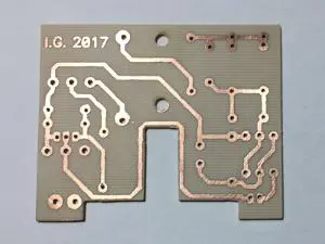
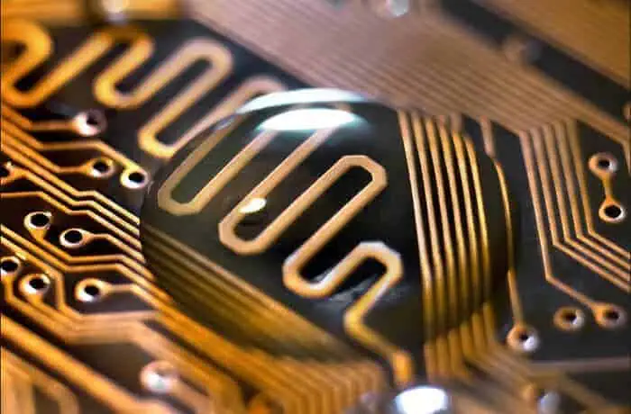
Printed circuit board etching involves the removal of any unwanted copper elements from a PCB circuit. The “unwanted” copper elements are simply the non-used copper elements in the circuit according to the board’s design. Therefore, manufacturers must etch out this unwanted copper to achieve that perfect circuit pattern.

Before the PCB etching process begins, manufacturers must get a presentation of the circuit’s layout defining the PCB’s final circuit. PCB designers transfer this layout image to the PCB manufacturer via a process called Photolithography. Manufacturers then utilize this image as a blueprint when deciding on the copper to remove and the one that remains on the board.

Two different etching approaches exist for the outer and the inner layers of a PCB. When etching outer layers of a PCB, manufacturers utilize tin plating to secure the parts that they do not want to etch. On the other hand, when etching the inner layer, manufacturers utilize a photoresist to protect the copper they do not want to remove.

Wet Etching (Isotropic)

Wet PCB etching is a simple technique that involves immersing the etching materials in a chemical solution to remove the excess copper. During this PCB etching process, three distinct factors affect the PCBโ€™s etching rate:

  • Etching chemical concentration
  • Etching solution temperature
  • Stirring the etching solution

Qualitatively speaking, if you wish to boost your PCB’s etching rate, you should increase the temperature of the etching solutions and include stirring during the process.

We carry out wet etching in two distinct methods, namely:

  • Alkaline etching
  • Acidic etching

Each of these methods bears its advantages and disadvantages.

Alkaline Etching Process and the Solution

Manufacturers utilize the alkaline etching process to remove (etch off) the PCB’s outer layer.

Solutions utilized in the Alkaline Etching Process

During this process, manufacturers utilize the following chemical solution to etch off copper elements from the outer part of the PCB:

  • Chloride Copper + Hydrochloride + water + Hydrogen Peroxide

When undertaking this PCB etching process, manufacturers must diligently follow all the parameters that make up this etching solution. That is because if they leave the board inside the solution for a long period, then the solution can easily damage the PCB. Therefore, there is need to control the process to avoid any bad occurrences.

Alkaline etching is pretty fast. However, it is also expensive.

How does the Alkaline Etching Process occur?

The entire process happens in a high-pressure spray chamber. In this chamber, there is thorough exposure of the PCB to an etchant spray.

During the alkaline etching process, manufacturers have to consider some crucial parameters, which include:

  • The movement rate of the panels
  • The etching spray
  • How much copper to remove from the PCB

When there is an optimum balance of these parameters, this etching process tends to be uniformly successful, bearing straight side walls and minimal errors.

When you remove every bit of unwanted copper from the PCB, the alkaline process hits a point known as the breakpoint. At this point, no more etching is supposed to take place. The breakpoint is, in most cases, reached when the PCB is at the spray chamber’s midpoint. For example, if the spay chamber has a total length of 2 meters, then the process will hit breakpoint when the PCB reaches the chamber’s midpoint, that is 1 meter.

The Acidic Etching Process

FULL PCB MANUFACTURING Quote

Manufacturers utilize the Acidic method to etch off unwanted copper elements from a rigid PCBโ€™s inner layer.

The Acidic process is cheaper, and it also achieves more precise results. However, this process also takes much time to achieve the desired circuit pattern compared to utilizing the alkaline etching method. The acidic process handles inner layer PCB etching because the acids do not react with photoresist. The acids do not damage crucial parts appearing on the PCB circuit blueprint. Moreover, this process does not breed many undercuts compared to the alkaline method.

An Undercut is a simple lateral erosion that occur below the etched material’s protective layer. When the etching solution hits the unwanted copper, it attacks it, leaving behind the copper layers that were protected using either:

  • Photo imaged resist or,
  • Plate etch-resist

At the edges of the tracks left behind, there are almost always some copper elements that one has removed. These elements leave structures known as undercuts.

Solutions utilized to undertake Acidic Etching

For this process to take place, manufacturers utilize the following chemical solvents:

Cupric Chloride Etching

PCB manufacturers mostly utilize Cupric Chloride to undertake acidic etching because it tends to etch off tiny features accurately. Moreover, this solution also provides continuous regeneration and constant etching, all at a pretty affordable price.

To maximize the etching rate of the Cupric Chloride process, manufacturers utilize a combination of cupric chloride-HCI chloride-sodium systems. Using this combination, manufacturers can achieve a max etching rate of about 55s for 10z when the copper is at 1300F. Due to these features, utilize this process to undertake fine line etching of inner layers.

Points to note when working with chlorine gas

When working with chlorine gas, ensure you do so in a well-ventilated room and also ensure you utilize the following equipment:

  • A tank
  • A cylinder storage
  • Leak detection equipment

Additionally, when utilizing chlorine, you will need emergency protocols, trained operators, approval to utilize the chemical from the area’s fire department, and personal protective equipment. All this features ensure that you stay safe when working with this chemical. Lagging in any of this precautions might lead to serious consequences.

Ferric Chloride PCB Etching process

Ferric Chloride is not utilized as much as Cupric Chloride in the PCB industry due to the cost of disposing of the hazardous waste that comes from the process. However, this solution is attractive in that:

  • It is super easy to use
  • Manufacturers can utilize it to handle infrequent batches
  • It has a great copper holding capacity

PCB manufacturers utilize Ferric Chloride solution with gold patterns, photoresist, and screen ink. However, donโ€™t use this chemical with lead/tin resist or tin.

In most cases, you dissolve Ferric Chloride in water with a concentration range of 42% – 28% by weight. After making this solution, manufacturers add about 5% of HCI into the mix to avoid insoluble precipitate formation of the now formed ferric hydroxide.

Finally, the acid content of this solution is usually between 1.5% – 2% for commercial usage.

Which parameters define an etchantโ€™s quality?

PCB-etching-materials

Ideally, etching rates depend on the time it takes to etch a PCB, assuming that the etching solution remains constant. However, this is not true. That is because the composition of an etchant changes continuously. Therefore, manufacturers must control certain parameters to ensure that the PCB etching process breeds a high-quality PCB. Here are some parameters that manufacturers use to assess an etchant’s quality to ensure that the etching process flows smoothly:

  • pH
  • Chemical additives
  • Baume
  • Oxidation-reduction potential
  • Temperature

Baume

Baume, or simply Be, is the molarity concentration of an etchant, and it depends upon the gravity of the solution.

A high Be usually coincides with high etchant molarity and ultimately a high etching rate. However, if the Baume of a solution is low, then that means that the solution’s molarity is low; hence the chemical will have a low etching rate.

A high Baume also reduces the number of undercuts formed after the etching process. Therefore, Baume is a crucial parameter to consider when working with any etchant.

Temperature

Generally, high temperatures improve the etch rate of an etchant. However, etching temperatures are constrained to the type of etching machine in use. Most etching machines utilize plastic parts since all metals tend to react with the etchant. Due to this reason, manufacturers tend to utilize low etching temperatures to avoid melting the plastic. The maximum etching temp range permitted falls between the range of 500 and 550C.

Chemical Additives

Most manufacturers utilize chemical additives to boost the etch rate of commercial etchants. For example, HCI is in common use as an additive for FeCL3 and CuCl2 etchants. When added to these solutions, HCI acts as chlorine’s source, generating metal chlorides rather than hydroxides. Due to this chemical reactions, these etchants can hold on to the dissolved metals.

Chemical additives are pretty crucial in the process of continuous etching. Manufacturers add them to their commercial etchant before utilizing it or during regeneration. However, they must first evaluate the solution’s pH to check its acidity before use.

Adding chemical additives to an etchant tends to improve its complexity, and it also boosts its etching rate. It also boosts the etchant’s dissolving capacity making it more reliable.

However, the amount of additive used in an etchant is constrained to the etching machine utilized. Therefore, adding a lot of Hydrochloric acid to the etchant might cause the acid in use to react with parts of the etching machine.

Oxidation-Reduction Potential

Printed Circuit Board manufacturers measure the oxidation-reduction potential of an etchant to determine its activity. Oxidation-reduction potential simply dictates an etchant’s relative conductivity, and we express it in millivolts.

Oxidation-reduction potential brings out the relationships that exist between:

  • Cuprous ions and Cupric ions
  • Ferrous ions and Ferric ions

As one removes the copper (etched), the chemical solution changes from a ferric/cupric to a ferrous/cuprous state.

An etchant with a high ORP is usually more efficient than an etchant with a low ORP.

Manufacturers maintain high ORP values to gain constant high etch rates. However, etching temperature and free acid contents influence the Oxidation-reduction potential values. Adding oxidizers and free acids into an etchant makes the solution breed chlorine. When this happens, the Cuprous formed earlier during the etching process revert to their initial cupric form.

PH Values

The pH of an etchant is a crucial etching parameter that you should greatly consider when working with etching solutions. It is especially crucial when you are undertaking alkaline etching. For reliable and efficient alkaline etching, the pH of the etching solution should fall between 7.9 to 8.1. A low pH that falls below 8 can be due to:

  • Low ammonia
  • Heating
  • Excessive ventilation et cetera

However, a high pH that goes above 8.8 can be caused by:

  • High copper contents
  • Under ventilation
  • Water found in the etchant

In acid etching, pH values are useful for solution control. A high pH causes incorrect copper colorimeter readings due to solution turbidity.

Pros of Wet Etching

The wet etching process has a couple of advantages that include:

  • It is cheaper compared to Dry etching
  • It breeds excellent surface uniformity
  • Better adaptability compared to dry etching
  • It has impeccable selectivity, hence it is mostly utilized for inner surface etching to achieve precision
  • A higher etching rate when compared to dry etching
  • The equipment used for wet etching is easy to maintain
  • Wet PCB etching can also take place under a normal atmospheric surrounding

Cons of Wet Etching

Even though Wet PCB etching is without a doubt beneficial, it still has some cons that include:

  • Pattern etching fidelity isnโ€™t ideal
  • Isotropic etching
  • Tiny lines of the board’s etching pattern are challenging to control
  • Toxic chemicals โ€“ might be due to indirect or direct fume exposure. It can also be due to direct liquid chemical exposure.
  • Risk of contaminating water

Conclusion

The etching process is, without a doubt, a crucial process in the production process of a PCB. Over the years, manufacturing companies have mastered the art of etching. However, evolution and industrialization have seen PCB circuits become more complex daily. Due to circuit complexity, the PCB etching process has also evolved, forcing manufacturers to look for ways to make etching solutions more productive. In the quest to make etchants productive, additive chemicals have been brought into the process to optimize etching solutions. In addition, manufacturers have also found ways to manipulate the pH of various etchants to make them more productive. PCB manufacturing has without a doubt been in optimal use by the improvements made in the PCB etching process, and we expect more improvements in the near future.

The Ultimate Guide to Choosing Xilinx XC2C64A-5VQ44C

Xilinx Spartan-6 FPGA

We want to be a part of your decision-making process for the Xilinx XC2C64A-5VQ44C. In this article, we aim to help you learn more about this Complex Programmable Logic Device (CPLD), including the features that matter the most.

Background to Xilinx XC2C64A-5VQ44Cโ€™s CPLD

A Complex Programmable Gate Array (CPLD), which Xilinx XC2C64A-5VQ44C is one of them, is a type of programmable logic device designed to provide the architectural features of the Field Programmable Gate Array (FPGA) and solving the complexity between the FPGA and PAL.

One outstanding feature of Xilinx XC2C64A-5VQ44Cโ€™s CPLD is that it uses a macrocell as its โ€œbuilding block.โ€ The macrocell is among many other things, responsible for implementing logics meant for both specialized logic operations and disjunctive normal form.

Technical Specifications

FULL PCB MANUFACTURING Quote

The technical attributes of the Xilinx XC2C64A-5VQ44C include, but are not limited to:

1. Speed

The speed grade for the Xilinx XC2C64A-5VQ44C CPLD is 5, while its propagation delay is pegged at 5 ns.

2. Operating Temperature

Xilinx XC2C64A-5VQ44C has its operating temperature between 0-degree Celsius and 70-degree Celsius. But that is not all because the CPLD can clock a maximum frequency of 263 MHz.

3. Voltage Supply

The supply and transmission of current within the Xilinx XC2C64A-5VQ44C CPLD is as important as the operating temperature.

The voltage supply rating is between 1.7 and 1.9 volts. It tends to have an average operating voltage supply of 1.8 volts.

4. Peripherals

Peripherals as used here refer to the components and designs that make up the Xilinx XC2C64A-5VQ44C. They include a ROMless memory type, 64 macrocells and 1,500 gates.

Features of Xilinx XC2C64A-5VQ44C

Looking for some of the features or characteristics that make Xilinx XC2C64A-5VQ44C a flexible and a better variant to FPGA and PLA?

Here are some of the CPLDโ€™s features:

Excellent Clocking Performance

This is one of the core features you want to look for. The clocking performance of the Xilinx XC2C64A-5VQ44C is not only multiple, but is also flexible.

For example, the CPLD features product term clocks. These are responsible for using the output to enable, set and reset the clocks.

The Xilinx XC2C64A-5VQ44C clocking performance is also adjudged by the multiple global clocks providing phase selection per macrocell. This forms a part of the basis for the global signal options with macrocell control.

The flexible clocking modes for Xilinx XC2C64A-5VQ44C are derived from the CoolCLOCK, Optional DualEDGE triggered registers and Clock dividers.

Advantages of Working with the Xilinx XC2C64A-5VQ44C CPLD

As a Complex Logic Programmable Device (CPLD), Xilinx XC2C64A-5VQ44C has lots of advantages and benefits to using it.

Here are some of the reasons why you should invest in it:

Stability is Assured

Stability in this case has to do with the programming of the CPLD. In that case, Xilinx XC2C64A-5VQ44C can maintain the previous programming without losing it โ€“ even when circuit is shut down.

Unlike the Field Programmable Gate Array (FPGA), Xilinx XC2C64A-5VQ44C doesnโ€™t use the SRAM memory architecture. That guarantees that information or data will remain in the circuit even if it is turned off or shut down.

Reduced Power Consumption

You donโ€™t need to invest so much to power the Xilinx XC2C64A-5VQ44C. Like every other CPLD out there, it can use low-power and still be efficient.

It is evident in the use of the CoolRunner-II architecture that permits the use of a minimal 50 uA current in most situations.

Data Security

How secure is the data or information stored in the Xilinx XC2C64A-5VQ44C? Most times, it is safer than the data stored in an FPGA.

It is possible because an FPGA uses external memory that could be susceptible to damage. On the contrary, Xilinx XC2C64A-5VQ44C CPLD uses the built-in storage/memory to keep the data โ€œin-house.โ€

Conclusion

We hope you enjoyed this guide to purchasing the Xilinx XC2C64A-5VQ44C CPLD. Now, go ahead and request a quotation from RayPCB to get an idea of the cost of designing the Complex Programmable Logic Device (CPLD) for you.

Xilinx XC2C384-10TQ144I Review: Technical Specifications & Features

Xilinx Spartan-7 FPGA

Xilinx XC2C384-10TQ144I is a CoolRunner-II Complex Programmable Logic Device (CPLD). Xilinx manufactures the series and has had it dedicated to chips optimized for higher performance, cost-effectiveness and low-power consumption.

For a detailed analysis of the Xilinx XC2C384-10TQ144I CPLD, read this article to the end.

What is a CPLD?

A Complex Programmable Logic Device (CPLD) is one of the popular programmable logic devices. The others are Field Programmable Gate Arrays (FPGAs), and Simple Programmable Logic Devices (SPLDs).

A CPLD is a type of programmable logic device that combines the features and functions of the Programmable Array Logic (PAL) with the Field Programmable Gate Array (FPGA).

It is also made up of several Programmable Array Logic (PAL) structures, which are called macrocells. These are the โ€œbuilding blockโ€ or โ€œcentral componentโ€ of the CPLD.

By default, the CPLD has all of the input pins pointing to the macrocell, while the macrocell has its dedicated output pin.

Introducing the Xilinx XC2C384-10TQ144I CPLD

FULL PCB MANUFACTURING Quote

Xilinx XC2C384-10TQ144I is a type of Complex Programmable Logic Device (CPLD) designed by Xilinx and categorized under the CoolRunner-II series.

In the subsequent sections of this article, you will find out some of the deviceโ€™s technical specifications, as well as the features.

Technical Attributes of Xilinx XC2C384-10TQ144I

Here are some of the technical attributes or components of the Xilinx XC2C384-10TQ144I CPLD:

1. Moisture Sensitivity Level

Moisture Sensitivity Level or MSL is the level of exposure the Xilinx XC2C384-10TQ144I CPLD is likely to be exposed to within a specific time. It is common if the device is exposed to ambient room conditions within this time, especially after it has been unveiled for use.

The rated MSL for Xilinx XC2C384-10TQ144I is 3 and this translates to 168 hours to be exposed to ambient room conditions from the time it is unveiled.

2. Type of Memory

Xilinx XC2C384-10TQ144I is a ROMless Complex Programmable Logic Device (CPLD). This means that it doesnโ€™t use the Random-Access Memory (RAM).

By default, when a programmable logic device is ROMless, it has to rely on an external memory. In that case, Xilinx XC2C384-10TQ144I sources data via external memory options, such as a hard drive, a flash drive or a Storage Device (SD) card.

3. Mounting Technology

Xilinx XC2C384-10TQ144Iโ€™s CPLD uses the Surface Mount Technology (SMT). The technology relies on Surface Mount Devices (SMDs), which are used to mount or place the required components atop the circuit.

4. Speed Grade

Speed grade, generally, is the delay or time it would likely take before the macrocell in the device can perform optimally. It is called in nanoseconds or ns.

The speed grade also marks or highlights the โ€œminimum guaranteed performance of the device.โ€ This is according to Xilinx. According to the manufacturer too, the rating doesnโ€™t necessarily cover the maximum performance of the chip.

Another important fact to note about the Xilinx XC2C384-10TQ144I CPLDโ€™s speed grade is that it is rated as 10. This means that it has a minimum delay of 10 nanoseconds to run through a macrocell.

Conclusion

In conclusion, Xilinx XC2C384-10TQ144I is one of the best Complex Programmable Logic Devices (CPLDs) you can invest your money in. For a guaranteed buying decision and professional advice, contact RayPCB.

How Xilinx Evaluation Board Impacts PCB Assembly

Xilinx Evaluation Board

When developing a printed circuit board, it is crucial you understand the purpose and intended use of the boards you are fabricating. This is the best way to make your PCB design to meet the performance and objectives for their utilization. However, these objectives may vary based on the type of board you are fabricating.

Let us look at what the Xilinx evaluation board does and how it affects PCBA development.

What is Xilinx Evaluation Board?

The Xilinx evaluation board helps to determine the suitability of a semiconductor component for an application. This board evaluates the performance and features of system solutions that demonstrate tested solutions for an application design. Also, the Xilinx evaluation board is specifically built around some parts.

These boards are primarily designed for design, evaluation, and testing purposes. Xilinx evaluation board offers all the fundamental components of design, IP, hardware, and tools that enable development. Also, evaluation boards aid the evaluation of some critical components. Therefore, these boards comprise a complex semiconductor like microprocessor unit (MCU) and sensor.

In addition, there are different types of output and input connectors and graphical displays. Xilinx designed an evaluation board to help evaluate components in a particular application. For instance, an evaluation board can interface with a power converter module. Furthermore, the use of evaluation boards enables a designer to assess the capabilities of a new product before including it to a new design.

The Xilinx evaluation board is a convenient way of developing a breadboard of a system without much custom hardware design. Also, you need to start with the basic requirements. The two most crucial requirements are processing capability and I/O.

Also, evaluation boards differ based on what they are evaluating. When choosing an evaluation board, you need to know the part you want to have first. Then, you can choose an evaluation board that has this part. Also, the major focus of an evaluation board is on the component.

When to Use the Xilinx Evaluation Board

  • You will need evaluation boards when you need to design a project quickly since it takes time to fabricate circuit boards. Also, you can develop most of your software before you get the PCB.
  • Also, evaluation boards are ideal when you need to build prototypes. Utilizing many evaluation boards can help to design an entire circuit before you start designing a circuit board. Therefore, this gives you the opportunity to have it working at first shot.
  • Xilinx evaluation boards are handy when there is a complex design to work with. Also, this evaluation board offers a starting point. Then, you can modify the software to execute what you need.
  • Also, an evaluation board can help you test the capability of a particular chip.

Xilinx Evaluation Board Hardware

Xilinx evaluation board is suitable for high-performance RF application and rapid prototyping. Also, this evaluation board is fully tested and assembled. The following sections define the various connectors on this board and the proper evaluation setup.

Input/output connectors

VIN test bus

The VIN test bus links the VIN pin to the positive input supply voltage. Connecting the power supply to this bus can keep the wires short to reduce EMI transmission.

GND Test Bus

This is the power ground connection for the part through the GND pin and also the bypass capacitors. Also, you can link ground connections from external equipment to the GND test bus.

EN Test Bus

The EN connector enables or disables the converter through the EN pin. Also, avoid leaving the EN pin floating.

VOUT Test bus

The resistive voltage divider network sets the output voltage at the VOUT test bus. Also, you can attach a load from the VOUT test bus to the GND test bus.

SW Test Point

This point helps to monitor the switching frequency and switch node behavior. Also, link a BNC cable to the test point. This helps to measure the switching frequency.

Evaluation Setup

For proper operation of the evaluation board, you need to:

  • Connect positive supply to VIN
  • Link the input supply ground to GND
  • Integrate a voltage between 2.5V and 5.5V to the VIN test bus.
  • Connect the load between GND and VOUT

Performance Evaluation

Line regulation

You can observe and measure line regulation by monitoring the output voltage.

Load regulation

You can observe and measure load regulation by monitoring the output voltage while sweeping the load between GND and VOUT. Also, you can utilize short low resistance wires to minimize voltage, particularly for heavy loads.

Load Transient

Evaluate the load transient performance by producing a fast current transient on the output. Also, observing the behavior of the evaluation board.

Oscillator frequency

Connect an oscilloscope to the SW pin to measure the oscillator frequency.

Line transient

Generate a high speed voltage transient on the input and check the behavior of the evaluation board at VOUT. With this, you can evaluate the performance of the line transient.

Inductor current

You can access the inductor current by getting rid of one side of the inductor from the pad. Then, connect a current loop in the series. Also, place an oscilloscope current probe on the loop to sew the waveform.

Efficiency

You need to compare the input power to output power to measure efficiency.

What is the Difference Between an Evaluation Board and a Development Board?

Evaluation boards and development are interchangeably used. An evaluation board primarily focuses on a component. On the other hand, a development board focuses on the functionality of the entire board. The design and manufacturing of an evaluation board include several types of interconnections. Also, evaluation boards utilize much space. These boards offer test points to help analyses and evaluation.

On the other hand, development boards feature additional circuitry to optimize the functionality range. Also, designers can manufacture a development board as a production board. The evaluation board determines the suitability of a semiconductor component for an application. A development board is the manufactured version of the evaluation board.

Conclusion

The Xilinx evaluation board offers great advantages and features for PCB assembly. Also, this evaluation board is widely used across industries like wireless communications and test & measurement.

Implementing Transmission Lines Impedance Calculator PCB

impedance control pcb

Most High-speed PCB designs can’t function properly if the Print Circuit Board designers miscalculate transmission line impedance. When bad calculations arise, traces that support high-speed edge rate signals eventually play the role of transmission lines, even though they are short. Therefore, the best practices in terms of nailing high-speed PCB designs state that you design the traces such that they are close to the set (required) impedance. Doing so minimizes return losses and helps yield a great PCB design.

To attain accurate results when calculating impedance, you can opt to perform the calculations manually or by hand. However, people have found that the most accurate formulas used to calculate impedance tend to be unwieldy when utilized in manual calculations.

Therefore, to help you start floor planning, we have compiled a list of impedance calculators that implement accurate impedance formulas. What’s more, once you have determined the rough estimation of the initial trace width needed to calculate the impedance of your PCB design. You can take things up a notch by utilizing a stack-up editor with an in-built impedance calculator to accurately calculate the required trace width.

Letโ€™s Explore More on Impedance

Impedance affects power transmission between various PCB components, signal propagation through a PCB, and how various signals bleed inside unwanted PCB areas. Several analyses exist which help you solve impedance. However, most of these methods don’t breed realistic results unless you utilize accurate parasitic elements. Therefore, when designing a simple circuit or working with a prototype for high-frequency or high-speed operations, you must be familiar with parasitic elements.

Another crucial factor to consider when looking for impedance is how non-linear circuits are affected by various levels of input signals. That is because impedance values of non-linear circuits are merely functions of an input.

What does impedance mean?

Impedance simply describes how electronic components behave when resisting an AC. Various circuits are built using different components, which all behave quite differently when exposed to an AC.

For starters, resistors have constant resistance under varying frequencies. That is because resistors are pure DC components. Therefore, the impedance of a resistor is merely its resistance.

Meanwhile, the impedance of a capacitor is simply its capacitive reactance. The capacitive reactance of a circuit is merely the inverse of the circuit’s angular frequency.

Therefore, when the circuit’s frequency increases, the capacitive reactance decreases.

Inductors, on the other hand, also behave like capacitors. However, they do have a slight difference in that the inductive reactance of a circuit is usually directly proportional to its angular frequency.

All these basic components are present in impedance analysis calculators. However, they are not the only components found on a circuit. Other components found on circuits that include transistors, diodes, and ICs all introduce impedance. Therefore, you have to factor in all of them in your calculations.

At advanced levels, traces also offers impedance because they are not long-term inductors. The PCB board also affects the circuit’s impedance. Hence calculating impedance can be pretty tedious.

Differential impedance is another factor you should probably consider when dealing with impedance. The differential impedance of a PCB is simply the current to voltage ratio on pairs of transmission lines driven in differential mode.

How does an Impedance Calculator Function to attain the Target Impedance

pcb impedance control

All transmission line calculators operate under the same principles. They all try to determine the impedance value of a generic transmission line geometry. As per how the calculators function, they implement the following methods:

  • Some of these calculators utilize the Telegrapher equations parameter (R, L, C) to accurately determine the transmission line impedance.
  • Others build varying models using experimental impedance information versus trace geometry. They then utilize the data that they get back to calculate impedance efficiently.
  • Other calculators utilize analytical techniques which provide dispersionless lossless impedance from famous Maxwellโ€™s equations.
  • Lastly, some of these calculators utilize the filed solver to solve Maxwellโ€™s equation electromagnetic field. They then utilize the field to work out impedance.

Most impedance calculators, especially the ones found online, utilize #2 (for calculators based on IPC-2141) or #3 (for more accurate calculations using the first principles).

You should note that, in case you have trouble accessing a field solver, then you should opt to utilize the #3 approach from above. Utilizing this method and the correct calculator application will, undoubtedly, breed accurate results.

Free Trace Line Impedance Calculators that utilize the #3 approach

The following impedance calculators are free to utilize. What’s more, these calculators return an accurate impedance value when as per the pairs of:

  • Copper weight values
  • Substrate thickness
  • Trace width

To utilize these to create a design for attaining desired impedance. You must cycle through different trace broadness geometric values until the impedance calculator returns your target value. The calculators include:

  • Differential Trace Stripline
  • Differential Trace Microstrip
  • Stripline Trace impedance
  • Microstrip Trace

These calculators utilize standard geometries utilized to create Print Circuit Board designs. While working with these calculators, if you choose a coplanar arrangement, you can easily approximate the trace routing by simply setting 10 mils. However, for this trick to work, the direct thickness has to be equal to or less than 10 mils.

The models utilized in these calculators base upon the Wadell equation, which is famous for providing pretty accurate impedance values (lossless). Even though the value they breed is not a hundred percent accurate for a couple of reasons. These models are pretty useful in terms of attaining quick trace impedance rough estimate values to utilize in the geometry equation.

The accuracy of an impedance calculator is affected by a couple of factors which include:

  • Parasitics (parasitic capacitance, to be specific)
  • Dispersion and dielectric losses
  • Copper roughness

When operating on a high frequency, the final values from the impedance calculator are not the same as those you will find on your PCB due to the above factors. This case occurs for a digital signal when the transmission line signalโ€™s rising edge becomes increasingly fast, concentrating signal contents on the GHz range. As per RF signals, this feature is crucial in the GHz range that exceeds 5.8 GHz.

Trace Width and its Relationship with exact impedance calculation

Differential Impedance

What exactly is a Trace?

A PCB trace is a thin line made up of copper found in the non-conductive area. You utilize the PCB trace to carry power and signal to the entire circuit.

Copper traces have different widths, and they all have a unique substrate height according to the design of the PCB.

Trace is a pretty crucial factor when it comes to designing Printed Circuit Boards. If you have designed a PCB before, you probably have faced complications when selecting the perfect trace broadness.

By default, beginners in the PCB designing industry mostly utilize the width provided by PCB designing software. At some point, this trick works. However, you must consider many factors affecting trace thickness when developing complex circuits.

How is Trace connected to impedance calculation?

Trace is directly connected to impedance calculation in more ways than one. For starters, a thin trace thickness brings about a high impedance value.

On the other hand, a large width usually brings about low impedance. Therefore, the thicker the PCB, the higher the impedance value and vice versa.

Parameters needed to Calculate Accurate Trace Impedance Values

To work out the trace impedance of a circuit, you will require the following parameters:

  • The trace thickness and width
  • Spacing between pair traces
  • Effective Dielectric constant of the dielectric component utilized in your PCB
  • The dielectric layer height between the reference planes and the signal trace

With this data, you can easily calculate the trace impedance of any PCB using an impedance calculator.

Other parameters to consider

When dealing with transmission lines, Characteristic impedance is a crucial parameter, probably the most crucial that you will encounter. Therefore, since impedance mostly circles around transmission lines, you should have prior knowledge on the same. A characteristic impedance is usually a material and a function of geometry. It is also a dynamic value that is independent of line length.

Carrying out Impedance Calculations using an Impedance Calculator

When working with an impedance calculator, you need first to select the correct impedance calculator mode. You should set the calculator mode according to the geometry of the relevant reference planes and the signal layer.

Most calculators draw trace geometries according to which layer the trace is found and how it is routed. So whether the PCB trace is on the top or bottom surface of the PCB or embedded inside different layers, you can easily choose the calculator mode that suits your design.

If you know your target impedance, then you can easily calculate the impedance value. You must type in your target impedance in the calculator, hit calculate, and the software does the rest.

Similarly, if you know the target trace broadness, then calculating the PCBs impedance is just as simple as calculating the width of the trace.

All you have to do is insert your target trace thickness inside an impedance calculator (mostly, the “insert target trace width text box” will be provided. Once you have keyed in your target trace width, you must click the “calculate impedance” button, and voila! You instantly get the impedance value.

And that is how you can easily calculate the impedance and trace width of any PCB with ease. Whatโ€™s more, every impedance calculator you find out there utilizes accurate formulas to ensure correct results each time.

Why should PCB Designers Strive to Control PCB Impedance?

The need for Increased Signal Power

A Print Circuit Board trace function by transferring signals from the source to the receiving end. For this transmission to take place, the signal must flow through a given trace length to reach the receiving end.

However, the PCB has to have matching impedance to achieve maximum signal power. Therefore, during corresponding layer construction you must utilize equal impedance to attain max signal power.

Improved Performance

PCB designs that employ impedance control perform faster than other PCBs and use less energy. Due to these features, the PCB tends to function better for longer. The electronics industry heavily utilizes impedance calculators to ensure electronics stay functional for longer.

Conclusion

Impedance calculation involves many parameters, and you must consider many factors to achieve accurate results. Due to these reasons, many engineers mess up the calculations and ultimately gain incorrect results that tamper with the PCBโ€™s quality. However, using an impedance calculator, you can easily tackle impedance problems and always attain accurate results each time.

Soldering Castellations PCB Mounting Holes

castellations pcb

Are you looking for a PCB that features castellated mounting holes? Are you wondering how to add these features to the PCB board? If so, then you’ve come to the right place. Read on to learn more.

Castellated Mounting Holes

When we make a circuit board, we refer to the mounting holes as castellated. In this type of design, there is the application of two different copper platings. A tin-plated PCB can have a thin layer of copper with a surface coating of anti-corrosion tin. The copper layer inside the castellated holes is then exposed. In addition to providing mechanical stability for the PCB, the copper-plated design eliminates the problems associated with copper skin and twisting.

Unlike other methods of PCB assembly, we can use castellated holes for combining two boards. This feature is especially useful for breakout boards, small modules, and PCB to PCB links. As a result, these PCBs have excellent compatibility and can be useful in various applications. You can also use these holes to make wireless PCB-to-PCB connections. As the name implies, castellated holes can be a great way to combine two boards into one.

There are several requirements for manufacturing castellated holes. The minimum diameter of the hole must be 0.6 mm. The minimum diameter of the holes must be identical to the hole diameter on the board outline/mechanical layer. If there are half holes, choose the “Yes” option and pay the extra fee. This option will require that the holes be at least 0.6 mm in diameter. If you choose “No,” there will be no additional fee for half-holes.

Castellated holes

half-hole-pcb
Half Hole PCB

Pad size is the most important factor when designing and creating castellated holes in PCBs. The most massive pads are best for these PCBs because they make it easier to align components. Moreover, the largest pads are also the best choice for castellated holes because you can drill them easily. This also reduces the risk of component liftoff and contamination during soldering. You can also make your own castellated holes by using the castellated hole features of Altium Designer.

The process of forming castellated holes is different from the traditional one. First, you need to drill the edge of the substrate plate. You will need to use specialized equipment for this step. Then, you should deposit a copper layer into the hole to ensure the excellent conductivity of the components. The whole process takes a few days, so you should make sure you hire a professional. Castellated holes in PCBs are an important part of many electronic devices, and you must ensure that the manufacturers you work with have the right skills and equipment for the job.

To meet the high standards of PCB manufacturing, manufacturers of castellated holes must be compliant with several design attributes. These include ENIG surface finish, large pads, and optimum hole numbers. Meeting these design attributes is essential for a successful end-product, as they can result in a faulty board.

Applications of Castellated holes

One of the most important considerations in PCBs’ manufacturing process is the hole’s size. To achieve the best results, use a minimum hole diameter of 1.0 mm, about 0.04 inches. Ideally, a castellated hole should be on the top or bottom of the boardโ€™s edge. Do not place it on the vertical board edge, as it will act as a bridge and hold the PCB in place.

Castellated holes are good for breakout boards in integrated modules in the manufacturing process. The castellated PCBs are capable of replicating specific components on a circuit board. For example, castellated PCBs can be useful to duplicate an inverter, filter, feedback loops, or any other part that requires multiple pins. In this way, castellated PCBs are flexible and can be mass-produced. They are also good as breakout boards, so users can change the pin layout of individual components as needed.

Apart from PCBs, castellated holes also allow the mounting of SMD components. This feature is especially useful for PCB boards with smaller diameters, as they are easier to work with and may not fit the standard PCB fabrication process. However, it is important to comply with the relevant certification standards before purchasing castellated holes. If you fail to do so, you risk getting a faulty board. But with castellated hole PCBs, this issue will not be a problem, as they are a popular choice for smaller PCB modules.

Half holes

In manufacturing a PCB, there is the plating of half holes. The holes must have an electrical connection. A physical connection is not enough โ€“ space the holes need with zero spacing between them. Even a small gap will affect soldering. However, plated half holes are not that hard to produce. So, you should be able to find an inexpensive PCB manufacturing company that can provide you with this feature.

To obtain a high-quality plated half-hole PCB, you should know how to recognize them. Half-holes are usually visible on the surface of a PCB, and the hole size is 0.55 mm or 0.06 mm, which is the actual size of two half-hole plates. Generally, a PCB manufacturer will supply you with a sample of these holes to ensure the quality of the board.

A Plated Half Hole PCB from Castellations is a great choice for all of your upcoming PCB projects. You manufacture this PCB with plated half holes, allowing electrical contact between its components. As PCB sizes decrease and geometric index increases, round holes are often insufficient to support the board’s components. Using a plated option, you’ll avoid the problems associated with cold soldering and achieve a superior electrical connection.

PCB Assembly Process

The Castellations PCB assembly process involves the formation of partial holes in the board through which you place electrical contacts. During proper alignment and assembly process, the thickness of the upper PCB is usually one-third the size of the lower one. Stacking can be more complicated if the holes are not parallel. It is therefore essential to stack the boards without creating any gaps. To improve the stacked PCBs, the copper layer on the hole’s wall must be similar to the size of the board’s component pads.

As with any other PCB, the holes of a castellated PCB must match the pads of the components it supports. If this is not possible, plate the holes in a different way and place the second row of through-holes. This way, you can mount the castellated PCB in a production castellated module. The next step is to determine where to locate the holes.

PCB board

A Castellations PCB board is a printed circuit board that uses two copper platings. The first copper plating is an anti-corrosion tin, which has to adhere to the substrate. The tin is removed by peeling off the board’s edge, exposing the copper of the Castellation holes. This process eliminates copper residue, copper skin, and twisting problems. Additionally, it reduces the amount of soldering flux used and can increase the reliability of the PCB.

As the density and functionality of electronic goods have increased, so has the soldering process. Many traditional processes require the soldering of round holes in the motherboard. This process can lead to cold solder, resulting in an inferior electrical connection. Many devices now incorporate plated half holes to ensure the PCB is properly conductive. A PCB with a large hole could cause an electronic product to fail. The Castellations PCB board is the ideal solution for these situations.

Surface Mount PCBs

To create castellated Surface Mount PCBs, it’s necessary to know the proper dimensions of the components and board layout. This way, you can size castellated PCBs to fit the space available. The holes in castellated circuit boards should be the largest possible sizes. If you use smaller holes, it can be difficult to align the components. It’s also important to check the size of the pads on the castellated board.

To make PCBs with castellated vias, you must have copper on the surface of the board and tin on the underlying substrate. For this process, you must indicate the copper through round pads, extending 40 mil from the edge of the board. Peel off the tin on the board, exposing the copper in the Castellation holes. In addition, this process eliminates copper skin and its twisting and curling problems.

The plated half holes on surface mount PCBs help turn them into a surface mount subassembly. These half holes are commonly useful as breakout circuits for fine-pitch SMD components. These holes also provide better soldering landings and eliminate space for dust. Semi-plated half holes are also widely used in microcontroller modules, display PCBs, and breakout PCBs.

The traditional process of using a solder mask and plated through holes on a PCB is no longer sufficient. As the density and multi-functionality of electronic goods increase, it’s vital to change the soldering process. A round hole plated with flux leads to cold solder that is not as good as a plated through hole. Large holes may also damage an electronic product, so plated half holes are becoming increasingly popular.

Breakout Board

In most cases, the breakout board for a bigger PCB will have a plated half-hole. This feature makes it possible to install various Printed Circuit Board modules without creating a void. It is also important for board-to-board connections. This hole style also allows for precision soldering and the development of a single PCB based on integrated modules.

It is important to select the correct surface finish for the castellated PCB. ENIG is the recommended finish for this type of board. The type of finish will depend on the intended application. For example, holes in castellated circuit boards should be the largest sizes available. Depending on the PCB design, it may be difficult to align pads. When choosing the size of holes, the manufacturer of the castellated PCB will make a recommendation for the appropriate number of holes.

Board to board soldering

This method can achieve a high level of reliability, which is necessary for high-reliability applications. However, there are a few things that you should keep in mind before you begin. Board to board soldering for castellations PCB requires that the pads on the main board be large enough to accept the entire solder fillet. Secondly, the solder mask must have a small enough expansion to prevent bridging.

The plated half-hole is an important aspect of the soldering process and needs precise positioning to ensure proper electrical contact. Otherwise, the solder will become weak. Lastly, it is important to avoid cold soldering, as this will result in an unreliable electrical link. A proper soldering process is essential to ensuring a strong, long-lasting connection when soldering a board to a main PCB board.

Castellation PCB and Plated Holes

If you’re in the market for a custom PCB with castellated holes, you’ve likely come across the solder mask opening. These openings occur where solder masks do not cover the copper layers of the board. These are important for castellation PCB users because they can prevent solder bridges between adjacent pads.

Traditional castellation holes are relatively simple to manufacture. Drilling and application of chemical copper are the first two steps. After that, they’re followed by pattern plating or panel plating, stripping the mask, and surface finishing. Afterward, the castellation process and outline milling complete the production process. Aside from assembling the PCBs, castellation PCB and Plated Holes can also be used to manufacture wireless PCB connections.

Placing flux on the surface of the board before soldering is an important step to ensure a quality assembly. Soldering flux on the board can cause flux residue to form. It will be amber, black, or sticky. To clean the board of flux, simply wipe it with rubbing alcohol. Also, using a Kimwipe to avoid lint on the board is recommended. Canned air is a good way to clean the board as well.

Wi-Fi Modules

There are many ways to solder the vias on a Castellations Wi-Fi Modules PCB. Some methods are known as Through Hole Technology (THT) or Surface Mount Technology (SMT). This process involves mounting a board on top of another PCB. Castellations are the links that connect the PCB to the module. You can use either method, depending on your needs. Regardless of your method, you must avoid too much solder to the connections.

Create Wireless PCB

The process of creating a wireless PCB with Castellations is relatively simple. You can treat the holes of the castellated board like through-hole components. The pads of the main board are large enough to accommodate the entire solder fillet, and the holes themselves are small enough to allow for the remaining solder fillet to fill the gap. This makes soldering the boards together easy. Before you begin, however, you should make sure that the pads of your main board are large enough to accommodate the entire fillet.

Start by creating a design that shows all the components and their connections. Then, you need to place the solder mask on the castellated PCB. This will prevent any problems with soldering, such as copper residue twisting. After you have done this, the next step will be to cut and mount the castellated PCB. This is a fairly simple process but can be a little time-consuming.

The Importance of PCB Inner Layer Clearance

PCB Inner Layer Clearance

When designing electronic circuit boards, it is important to consider the inner layer clearance. This measurement measures the smallest distance between two conductors on the board. We can calculate the inner layer clearance using an appropriate software application. You will also need to consider creepage, the separation between the conductors along the board’s surface or layers. The minimum creepage value for a given board is 0.6mm.

To avoid any issues, it’s a good idea to drill a pair of vias at the inner layers of your printed boards (for example in the layer stackup 2:2:2:1) to run wiring from the top to the bottom. What’s the benefit? The clearance between internal layers is important to help prevent shorts and ensure that components on these layers will not be damaged when soldering.

Printed Circuit Board and the Annular Ring

The Printed Circuit Board (PCB) and the Annular Ring play an important role in a circuit board’s overall design and functionality. These two components are interdependent, and their precise dimensions make them essential for the smooth functioning of any circuit. However, they can be a little tricky to design correctly. Let’s consider the most important things when designing an annular ring.

First, ensure that the vias are large enough for the components on the PCB. The width of the annular ring should be at least 10 mils, so it can approach the via with a tolerance of five millimeters. You can place a small ring on the circuit board, but we recommend one that is very large. Instead, you can use multiple smaller vias.

Next, you must consider the mounting scheme of the elements on the board. The through-hole mounting scheme includes inserting the elements’ leads into holes on the printed circuit board. It requires minimal fuss and few errors like accidentally bringing about bridges. There are two types of annular rings, the Outer and the Inner. You should choose the right one based on the type of application you have in mind.

Minimum Annular Ring

The Minimum Annular Ring clearance for PCBs is important to avoid rupture issues. An annular ring acts as an interconnect node and determines the conductivity of the board. The diameter of the annular ring should be less than the board width, but wide enough to maintain a reliable connection. Although the PCB manufacturers set a tolerance for the annular ring size, many designers opt for a bit extra to avoid issues down the line.

The Minimum Annular Ring clearance for PCB inner layers is critical for the proper spacing of wires and leads. It also serves as an anchor for the circuit. A PCB manufacturer will have a standard tolerance for the Minimum Annular Ring diameter, usually within 5 miles. An ideal annular ring is dead center, and dead center alignment ensures excellent connectivity between the various layers and vias. In addition, the Minimum Annular Ring clearance for PCB inner layer requires proper setting during the design stage.

How to Choose the Right Annular Ring Width for Your PCB Design

To choose the right ring width for your PCB design, you’ll need to understand what the specifications are for each component. For instance, for low to medium current, you should choose a component with an annular ring width of about 0.3mm. For higher current, you’ll need to gradually increase the hole diameter and the annular ring’s meatiness. This measurement is dependent on the accuracy of the component supplier.

Another important parameter is the hole diameter. For PCB designs, the minimum diameter will depend on the capabilities of the PCB manufacturer and the nature of the hole, including plating. Copper pads are useful to connect traces. Often, one drills a via at the pad’s center. The annular ring surrounds this via. An annular ring must be at least as wide as the copper pads on the PCB.

Solidly connect the copper pad surrounding the via. In addition, a properly drilled copper pad will act as an anchor for the PCB.

Minimum Trace Width

PCB manufacturers ensure that signal traces are the right size for their designs. While choosing a trace width, it is important to remember that too wide of a trace will lead to problems during PCB production and operation. In particular, we do not recommend trace widths of 3 mils because not all fabricators can successfully construct them. This narrow trace width is also unsuitable for long-distance escape routing beneath dense BGA components. Generally, a trace width of five mils is sufficient for most signal traces.

When determining the proper trace width, it is essential to consider the overall PCB layout. The minimum trace width should be around 0.012″ or less. Alternatively, the trace width should be as small as possible. When choosing the optimum trace width, make sure to choose a direct and short path, and leave enough space between it and the edge of the layer. Typically, 10 to 15 mils of space is commendable.

When choosing a PCB trace width, it is important to keep in mind the IPC standards. IPC-2152 outlines the current limit for PCB traces based on empirical data. When evaluating the PCB trace width, the table is a good place to start. It will give you an upper limit on the maximum current that a trace can carry. For more detailed analysis, a simulation is needed. Nevertheless, for typical boards, IPC tables are good enough.

PCB Minimum Spacing

The minimum space between parallel traces is an important mechanical specification in the fabrication of electronic circuit boards. It is a critical issue when devices are dense, since small space will result in crosstalk. To reduce this effect, minimum separation should be wide enough to provide a good ground return path. Printed circuit board thickness and material influence minimum spacing.

PCB Trace and Finished Hole

The width of the PCB trace and finished hole depends on the signal on transmission. Thin traces are used when high current and noise protection are not required. They are most commonly useful in circuit boards. You can use thicker traces for peripherals and high-power circuits depending on the signal. Thinner traces are good when the board has limited space. Finished holes are good when you need to populate the board with components.

PCBs have 3 kinds of holes: trace, plated hole, and NPTH. One makes each hole differently. In general, non-plated holes are drilled with a different bit size than plated holes. Non-plated holes with copper pads are not part of NPTH status. The PCB trace and plated hole size must be within the same range for a correct fit.

Wide traces affect the solderability of components because they act as heat sinks. In addition, they can make a component smolder unsuitable because of poor solder joints. Wide traces are also problematic because you can connect small two-pin parts to a large metal area on one pad and a thin trace on the other. This situation is called tombstoning, and it requires manual rework to correct it.

A drilled hole is an opening created in a PCB board where one places the metal pads. This opening typically has a diameter of 0.5mm, the size of most pins. Most designers know that drilled holes play a vital role in electrical engineering and PCB design; but what most people don’t know is how to properly lay out the drilled hole on their boards. IPC guidelines outline a specific method for creating drilled holes.

High Voltage and Working Voltage

To determine the inner layer clearance of a PCB, the manufacturer must first know the high and working voltages for the circuit board. The working voltage of the circuit board and its corresponding high voltages can vary widely, so the optimum inner layer clearance can be different for different voltages and circuit boards. The IPC-2221 standard defines the rules for PCB inner layer clearances. This standard covers the most critical details of the PCB design, including electrical clearances, board shape, and mounting holes. These parameters will determine the mechanical support and placement of components.

The external layers must be sufficiently clear for high voltage PCBs to prevent creepage. The inner layer clearances should be less than the outer layers’ thickness, but not less than the inner layer. However, the outer layers need not be identically aligned and can overlap if you meet creepage conditions. The main reason for see-through gaps is aesthetics, as they do not use extra copper. However, the electrical reasons for inner layer clearances are less prominent. A practical adjustment is to increase the thickness of the substrate. For example, if the board will have a higher hazardous voltage, the pre-preg thickness should be increased.

Design files are a common step in PCB production. They are important in ensuring that the board is well-planned and assembled properly due to their size and the many generations of the files. EDA software has recently become more advanced, which means one can create many design files on computer systems. Unfortunately, this often means there is less room for documentation for each layer in the file itself. This becomes an issue when holes are drilled through these layers because it can lead to peak voltage below accepted values or other unexpected consequences.

Safety Standards and the Altium Designer

Altium Designer helps engineers comply with Safety Standards, and helps design teams find and use quality components. The Altium Designer’s Bill of Materials (BOM) features automatically check items for violations of the standard and include accurate supplier and cost information. This ensures that designs meet compliance requirements, and Altium helps designers collaborate with multi-functional teams.

In the Altium software, you can use advanced tools to check for signal integrity violations, such as mismatched net controlled impedance. You can also perform signal integrity screening with the PDN analyzer, a design rule system that helps identify and correct signal integrity violations. The designer also helps engineers implement Design for Manufacturing (DFM) principles and offers smart component placement.

Altium’s safety standards support program is part of its ongoing commitment to helping users create safe and reliable systems. Embedded software is a critical path in many automobile systems.

The pollution degree of a PCB can either be high or low, and varies based on the type of application. Pollution degree 1 means there is no pollution; degree 2 means no pollution at all, but that contamination may be conductive or become conductive through condensation. Pollution degree 3 is a pollution problem, and it’s highly likely conductive. We can determine the pollution degree of a PCB by its material group, which reflects its electrical breakdown and tracking properties.

Contract Manufacturer and PCB Trace

A contract manufacturer understands PCB materials and the PCB manufacturing process. They can help you design and bring your PCB through the entire manufacturing process. A PCB trace helps ensure that your PCB will be manufactured as specified and is an essential part of your final product. However, a PCB trace is not a substitute for the printed circuit board itself. Therefore, the inner layer of your PCB must be completely clear.